bq25910 i2c controlled 6-a three-level switch mode, … · 4 bq25910 slvsdu0a–september...
TRANSCRIPT

HostHost
Control
VBUS
SW
BATP
BATN
I2C Bus
+
CFLY±
CFLY+
USB VBUS SW
BTST
SYS
BAT
Master
bq25910
Host Control
I2C Bus
Copyright © 2017, Texas Instruments Incorporated
ICHG
Product
Folder
Order
Now
Technical
Documents
Tools &
Software
Support &Community
An IMPORTANT NOTICE at the end of this data sheet addresses availability, warranty, changes, use in safety-critical applications,intellectual property matters and other important disclaimers. PRODUCTION DATA.
bq25910SLVSDU0A –SEPTEMBER 2017–REVISED FEBRUARY 2018
bq25910 I2C Controlled 6-A Three-Level Switch Mode,Single-Cell Parallel Battery Charger for Fast Charging
1
1 Features1• Parallel Charger Operation Provides Fast
Charging in Dual Charger Configuration• High Efficiency 750-kHz Switch Mode Three-Level
Buck Parallel Charger– Reduced Ripple to Support Low Profile
Inductor– 95.4% Charge Efficiency at 1.5 A from 5-V
Input– 93.3% Charge Efficiency at 3 A from 9-V Input– Superior Efficiency Compared to Traditional
Buck Converter in Compact Form Factor• Single Input to Support USB Input and Adjustable
High Voltage Adapters– Support 3.9-V to 14-V Input Voltage Range
with 20-V Absolute Maximum Input VoltageRating
– Input Current Limit (500 mA to 3.6 A with 100-mA resolution) to Support USB2.0 and USB3.0 Standard and High Voltage Adaptors
– Maximum Power Tracking by Input VoltageLimit (VINDPM) up to 14 V
• Flexible I2C Mode for Optimal SystemPerformance
• High Integration Includes all MOSFETs, CurrentSensing and Loop Compensation– Lossless Charge Current Sensing without
Sense Resistor• < 10-µA Low Battery Leakage Current During
Stand-By Mode• High Accuracy
– ±0.4% Charge Voltage Regulation– ±10% Charge Current Regulation– ±7.5% Input Current Regulation– Remote Differential Battery Sensing
• Safety– Thermal Regulation and Thermal Shutdown– Input UVLO and Overvoltage Protection– Battery OVP– Input Dynamic Power Management (DPM)– Charging Safety Timer– Flying Capacitor Short Circuit Protection– Output Voltage Short Circuit Protection
• Available in 36-Ball WCSP Package
2 Applications• Smart Phone• Tablet• Wireless Charging• Portable Electronics• Electronic Point of Sales (ePOS)
3 DescriptionThe bq25910 is an integrated three-level switch-modeparallel battery charge management device for singlecell Li-ion and Li-polymer batteries. Utilization of thethree-level converter maintains highest switch-modeoperation efficiency while reducing solution footprintand increasing power density. The device supportsfast charging with high input voltage for a wide rangeof portable devices. The solution integrates reverse-blocking FET (QBLK), and four switching FETs (QHSA,QHSB, QLSB, QLSA). The I2C serial interface withcharging and system settings makes the device atruly flexible solution.
Device Information(1)
PART NUMBER PACKAGE BODY SIZE (NOM)bq25910 DSBGA (36) 2.41 mm x 2.44 mm
(1) For all available packages, see the orderable addendum atthe end of the data sheet.
Simplified Schematic

2
bq25910SLVSDU0A –SEPTEMBER 2017–REVISED FEBRUARY 2018 www.ti.com
Product Folder Links: bq25910
Submit Documentation Feedback Copyright © 2017–2018, Texas Instruments Incorporated
Table of Contents1 Features .................................................................. 12 Applications ........................................................... 13 Description ............................................................. 14 Revision History..................................................... 25 Pin Configuration and Functions ......................... 36 Specifications......................................................... 5
6.1 Absolute Maximum Ratings ...................................... 56.2 ESD Ratings.............................................................. 56.3 Recommended Operating Conditions....................... 66.4 Thermal Information .................................................. 66.5 Electrical Characteristics........................................... 76.6 Timing Requirements .............................................. 106.7 Typical Characteristics ............................................ 11
7 Detailed Description ............................................ 137.1 Overview ................................................................. 137.2 Functional Block Diagram ....................................... 147.3 Feature Description................................................. 157.4 Device Functional Modes........................................ 21
7.5 Programming .......................................................... 247.6 Register Maps ......................................................... 28
8 Application and Implementation ........................ 438.1 Application Information............................................ 438.2 Typical Application ................................................. 43
9 Power Supply Recommendations ...................... 5010 Layout................................................................... 51
10.1 Layout Guidelines ................................................. 5110.2 Layout Example .................................................... 52
11 Device and Documentation Support ................. 5311.1 Device Support...................................................... 5311.2 Receiving Notification of Documentation Updates 5311.3 Community Resources.......................................... 5311.4 Trademarks ........................................................... 5311.5 Electrostatic Discharge Caution............................ 5311.6 Glossary ................................................................ 53
12 Mechanical, Packaging, and OrderableInformation ........................................................... 53
4 Revision History
Changes from Original (September 2017) to Revision A Page
• Changed from Advance Information to Production Data ....................................................................................................... 1

VBUS PMID CFLY+ SW CFLY±
VBUS PMID CFLY+ SW
VBUS PMID CFLY+ SW CFLY±
CDRV+ PMID CFLY+ SW CFLY±
CDRV± SDA INT SW
SCL CAUX REGN BATN BATP
A
1 2 3 4 5
B
C
D
E
F
GND
GND
GND
IND_SNS
GND
6
CFLY±
CFLY± GND
x
3
bq25910www.ti.com SLVSDU0A –SEPTEMBER 2017–REVISED FEBRUARY 2018
Product Folder Links: bq25910
Submit Documentation FeedbackCopyright © 2017–2018, Texas Instruments Incorporated
5 Pin Configuration and Functions
bq25910-YFF (I2C controlled)36-Pin DSBGA
Top View
(1) Top View = Xray through a soldered down part with A1 starting in upper left hand corner.

4
bq25910SLVSDU0A –SEPTEMBER 2017–REVISED FEBRUARY 2018 www.ti.com
Product Folder Links: bq25910
Submit Documentation Feedback Copyright © 2017–2018, Texas Instruments Incorporated
Pin FunctionsPIN
I/O DESCRIPTIONNAME NO.
BATN F4 AI Negative Battery Sense Terminal – Kelvin connect via 100-Ω resistor as close as possibleto negative battery terminal
BATP F5 AI Positive Battery Sense Terminal – Kelvin connect via 100-Ω resistor as close as possibleto positive battery terminal
CAUX F2 P Auxiliary Capacitor – Bypass CAUX to GND with at least a 4.7-μF, 10-V ceramic capacitor
CDRV+ D1 PGate Drive Supply Positive Terminal – CDRV is used to generate multilevel gate driverails.Connect a 220-nF, 6.3-V ceramic capacitor across CDRV+ and CDRV-.
CDRV– E1 PGate Drive Supply Negative Terminal – CDRV is used to generate multilevel gate driverails.Connect a 220-nF, 6.3-V ceramic capacitor across DRV+ and DRV-.
CFLY+
A3
PFlying Capacitor Positive Terminal – Connect 20-μF, 16-V ceramic capacitor acrossCFLY+ and CFLY–. Refer to Application and Implementation section for more information onselecting CFLY.
B3C3D3
CFLY–
A5
PFlying Capacitor Negative Terminal – Connect 20-μF, 16-V ceramic capacitor acrossCFLY+ and CFLY–. Refer to Application and Implementation section for more information onselecting CFLY.
B5C5D5E5
GND
A6
- Ground ReturnB6C6D6E6
IND_SNS F6 AI Output Inductor Sense Input – Kelvin connect as close as possible to the output of theswitched inductor.
INT E3 DO Open-Drain Interrupt Output – Connect INT to the logic rail via a 10-kΩ resistor. The INTpin sends active low, 256-μs pulse to the host to report charger device status and fault.
PMID
A2
PReverse Blocking MOSFET and QHSA MOSFET Connection – Given the total inputcapacitance, place 1 μF on VBUS, and the rest on PMID, as close to the device as possible.Typical value: 10-μF, 25-V ceramic capacitor
B2C2D2
REGN F3 P Gate Drive Supply – Bias supply for internal MOSFETs driver and device. Bypass REGN toGND with a 4.7-μF, 10-V ceramic capacitor.
SCL F1 DI I2C Interface Open-Drain Clock Line – Connect SCL to the logic rail through a 10-kΩresistor.
SDA E2 DIO I2C Interface Open-Drain Data Line – Connect SDA to the logic rail through a 10-kΩresistor.
SW
A4
PInductor Connection – Connect to the switched side of the external inductor(Recommended: 330 nH for up to 9-V applications or 470 nH for up to 12-V applications).Refer to Application and Implementation section for more information on selecting inductor.
B4C4D4E4
VBUSA1
P Input Supply – VBUS is connected to the external DC supply. Bypass VBUS to GND with atleast 1-μF, 25-V ceramic capacitor, placed as close to the device as possible.B1
C1

5
bq25910www.ti.com SLVSDU0A –SEPTEMBER 2017–REVISED FEBRUARY 2018
Product Folder Links: bq25910
Submit Documentation FeedbackCopyright © 2017–2018, Texas Instruments Incorporated
(1) Stresses beyond those listed under Absolute Maximum Ratings may cause permanent damage to the device. These are stress ratingsonly, which do not imply functional operation of the device at these or any other conditions beyond those indicated under RecommendedOperating Conditions. Exposure to absolute-maximum-rated conditions for extended periods may affect device reliability.
(2) This condition is contingent on the fact that 0V < VCFLY < 8V
6 Specifications
6.1 Absolute Maximum Ratingsover operating free-air temperature range (unless otherwise noted) (1)
MIN MAX UNIT
Voltage range (withrespect to GND)
VBUS (converter not switching) –2 20 VPMID (converter not switching) –0.3 20 VCDRV+, CDRV- –0.3 20 VCFLY+ –0.3 16 (2) VCFLY+ to SW, SW toCFLY–, CFLY– to GND,CAUX to GND
DC –0.3 7 V
Pulse < 30ns –0.3 11 V
BATP, BATN, IND_SNS –0.3 6 VREGN –0.3 6 V
Voltage range (withrespect to GND) SDA, SCL, /INT –0.3 6 V
Output sink current /INT 6 mAJunction Temperature, TJ –40 150 °CStorage temperature, Tstg –40 150 °C
(1) JEDEC document JEP155 states that 500-V HBM allows safe manufacturing with a standard ESD control process.(2) JEDEC document JEP157 states that 250-V CDM allows safe manufacturing with a standard ESD control process.
6.2 ESD RatingsVALUE UNIT
V(ESD) Electrostatic discharge
Human body model (HBM), perANSI/ESDA/JEDEC JS-001 (1) ±2000 V
Charged device model (CDM), per JEDECspecification JESD22-C101 (2) ±250 V

6
bq25910SLVSDU0A –SEPTEMBER 2017–REVISED FEBRUARY 2018 www.ti.com
Product Folder Links: bq25910
Submit Documentation Feedback Copyright © 2017–2018, Texas Instruments Incorporated
(1) The inherent switching noise voltage spikes should not exceed the absolute maximum rating on either CFLY+, SW, or CFLY- pins. Atight layout minimizes switching noise.
6.3 Recommended Operating Conditionsover operating free-air temperature range (unless otherwise noted) (1)
MIN NOM MAX UNITVVBUS Input voltage 3.9 14 (1) VIVBUS Average input current (VBUS) 3.3 AISW Average output current (SW) 6 AVBAT Battery voltage (BATP - BATN) 4.775 VTA Operating free-air temperature –40 85 °C
(1) For more information about traditional and new thermal metrics, see the Semiconductor and IC Package Thermal Metrics applicationreport, SPRA953.
6.4 Thermal Information
THERMAL METRIC (1)bq25910
UNITYFF (DSBGA)36-PINS
RΘJA Junction-to-ambient thermal resistance 52.8 °C/WRΘJC(top) Junction-to-case (top) thermal resistance 0.3 °C/WRΘJB Junction-to-board thermal resistance 11.1 °C/WΨJT Junction-to-top characterization parameter 0.2 °C/WΨJB Junction-to-board characterization parameter 11.1 °C/W

7
bq25910www.ti.com SLVSDU0A –SEPTEMBER 2017–REVISED FEBRUARY 2018
Product Folder Links: bq25910
Submit Documentation FeedbackCopyright © 2017–2018, Texas Instruments Incorporated
6.5 Electrical CharacteristicsVVBUS_UVLOZ < VVBUS < VVBUS_OV and VVBUS > VBAT + VSLEEP, TJ = –40°C to +125°C, and TJ = 25°C for typical values (unlessotherwise noted)
PARAMETER TEST CONDITIONS MIN TYP MAX UNITQUIESCENT CURRENTS
IBATBattery discharge current (BATP,BATN, SW)
VBAT = 4.5V, VBUS = 0 - 5V, SCL, SDA =0V or 1.8V, TJ < 85°C, EN_CHG = 0 6.5 10 μA
IVBUS_HIZ Input supply current (VBUS) in HIZVBUS = 5V, High-Z Mode, no battery 30 μAVBUS < VVBUS_OV, High-Z Mode, nobattery 50 μA
IVBUS Input supply current (VBUS)
VBUS > VSLEEPZ, VBAT = 3.8V, ICHG = 0A,converter not switching 20 μA
VBUS > VSLEEPZ, VBAT = 3.8V, converterswitching, IOUT = 0A 13 mA
VBUS / VBAT POWER UPVVBUS_OP VBUS operating range 3.9 14 VVVBUS_UVLOZ VBUS rising for active I2C, no battery VBUS rising 3.6 V
VSLEEP Enter sleep mode threshold VBUS falling, VBUS - VBAT,VBAT = 4V, TJ = 0°C - 85°C 15 60 110 mV
VSLEEPZ Exit sleep mode threshold VBUS rising, VBUS - VBAT,VBAT = 4V, TJ = 0°C - 85°C 115 220 275 mV
VVBUS_OVVBUS over-voltage rising threshold VBUS rising 14 14.3 14.7 VVBUS over-voltage falling threshold VBUS falling 13.3 13.65 14 V
VBAT_UVLOZ Battery for active I2C, no VBUS 2.3 VVPOORSRC Bad adapter detection threshold 3.7 VIPOORSRC Bad adapter detection current source 20 mAPOWER-PATH
RON_QBLK (QBLK)Top reverse blocking MOSFET on-resistance between VBUS and PMID(QBLK)
TJ = –40°C - 125°C 14 22 mΩ
RON_QHSA (Q1)Outer, high-side switching MOSFETon-resistance between PMID andCFLY+ (Q1)
TJ = –40°C - 125°C 22 40 mΩ
RON_QHSB (Q3)Inner, high-side switching MOSFETon-resistance between CFLY+ andSW (Q3)
TJ = –40°C - 125°C 12 20 mΩ
RON_QLSB (Q4)Inner, low-side switching MOSFETon-resistance between SW andCFLY- (Q4)
TJ = –40°C - 125°C 8 13 mΩ
RON_QLSA (Q2)Outer, low-side switching MOSFETon-resistance between CFLY- andGND (Q2)
TJ = –40°C - 125°C 8 13 mΩ
BATTERY CHARGER
VREG_RANGETypical charge voltage regulationrange 3.5 4.775 V
VREG_STEPTypical charge voltage regulationstep 5 mV
VREG_ACC Charge voltage regulation accuracy VREG = 4.2V or 4.35V or 4.4V,TJ = –40°C - 85°C -0.4 0.4 %
ICHG_RANGETypical charge current regulationrange 1000 6000 mA
ICHG_STEPTypical charge current regulationstep 50 mA
ICHG_ACC Charge current regulation accuracy ICHG = 2A, 3A, 4A, 5A, 6A,TJ = –40°C - 85°C -10 10 %

8
bq25910SLVSDU0A –SEPTEMBER 2017–REVISED FEBRUARY 2018 www.ti.com
Product Folder Links: bq25910
Submit Documentation Feedback Copyright © 2017–2018, Texas Instruments Incorporated
Electrical Characteristics (continued)VVBUS_UVLOZ < VVBUS < VVBUS_OV and VVBUS > VBAT + VSLEEP, TJ = –40°C to +125°C, and TJ = 25°C for typical values (unlessotherwise noted)
PARAMETER TEST CONDITIONS MIN TYP MAX UNIT
ITERM_ACCTermination current regulationaccuracy
VBUS = 9V, ICHG = 4A, ITERM = 1.0A,TJ = 0°C - 85°C 0.9 1 1.1 A
VBAT_SHORT Short battery voltage falling threshold VBAT falling 1.85 2.00 2.15 V
VBAT_LOWV
VBAT LOWV Rising threshold tostart fast-charging VBAT rising, VBATLOW = 3.2V 3.1 3.2 3.3 V
VBAT LOWV Falling threshold tostop fast-charging VBAT falling, VBATLOW = 3.2V 2.9 3 3.1 V
VBAT_LOWV
VBAT LOWV Rising threshold tostart fast-charging VBAT rising, VBATLOW = 3.5V 3.4 3.5 3.6 V
VBAT LOWV Falling threshold tostop fast-charging VBAT falling, VBATLOW = 3.5V 3.2 3.3 3.4 V
RBATP BATP Input resistance VBAT = 4V, VBUS = 5V, EN_CHG = 0 0.6 MΩ
RBATN BATN Input resistance VBAT = 4V, VBUS = 5V, EN_CHG = 0 0.6 MΩ
INPUT VOLTAGE / CURRENT REGULATIONVINDPM_RANGE Input voltage regulation range 3.9 14 VVINDPM_STEP Input voltage regulation step 100 mV
VINDPM_ACC Input voltage regulation accuracyVINDPM = 4.3V 4.121 4.3 4.447 VVINDPM = 7.8V 7.566 7.8 8.034 VVINDPM = 10.8V 10.476 10.8 11.124 V
IINDPM_RANGE Input current regulation range 500 3600 mAIINDPM_STEP Input current regulation step 100 mA
IINDPM_ACC Input current regulation accuracy
IINDPM = 500mA, TJ = –40°C - 85°C 410 500 mAIINDPM = 1500mA, TJ = –40°C - 85°C 1275 1500 mAIINDPM = 2500mA, TJ = –40°C - 85°C 2125 2500 mAIINDPM = 3000mA, TJ = –40°C - 85°C 2540 3000 mA
BATTERY OVER-VOLTAGE PROTECTION
VBAT_OVPBattery over-voltage rising threshold VBAT rising, as percentage of VREG 102 104 106 %Battery over-voltage falling threshold VBAT falling, as percentage of VREG 100 102 103 %
THERMAL REGULATION AND THERMAL SHUTDOWN
TREGJunction temperature regulationaccuracy
TREG = 80°C 80 °CTREG = 120°C 120 °C
TSHUTThermal Shutdown Rising threshold Temperature Increasing 150 °CThermal Shutdown Falling threshold Temperature Decreasing 120 °C
BUCK MODE OPERATIONFSW PWM switching frequency Switching-node frequency 1.35 1.5 1.65 MHzDMAX Maximum PWM Duty Cycle 97 %REGN LDO
VREGN REGN LDO output voltageVVBUS = 12V, IREGN = 40mA 4.85 5 VVVBUS = 5V, IREGN = 20mA 4.7 4.8 V
IREGN REGN LDO current limit VVBUS = 5V, VREGN = 3.8V 50 mA
9
bq25910www.ti.com SLVSDU0A –SEPTEMBER 2017–REVISED FEBRUARY 2018
Product Folder Links: bq25910
Submit Documentation FeedbackCopyright © 2017–2018, Texas Instruments Incorporated
Electrical Characteristics (continued)VVBUS_UVLOZ < VVBUS < VVBUS_OV and VVBUS > VBAT + VSLEEP, TJ = –40°C to +125°C, and TJ = 25°C for typical values (unlessotherwise noted)
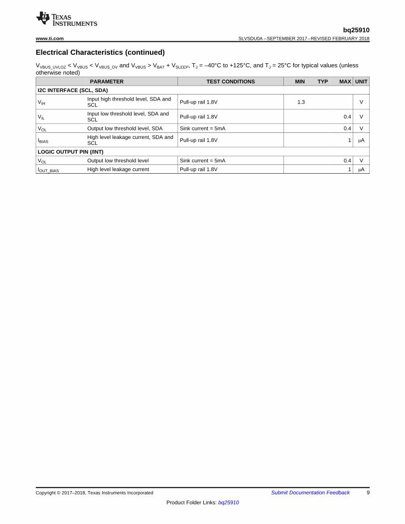
PARAMETER TEST CONDITIONS MIN TYP MAX UNITI2C INTERFACE (SCL, SDA)
VIHInput high threshold level, SDA andSCL Pull-up rail 1.8V 1.3 V
VILInput low threshold level, SDA andSCL Pull-up rail 1.8V 0.4 V
VOL Output low threshold level, SDA Sink current = 5mA 0.4 V
IBIASHigh level leakage current, SDA andSCL Pull-up rail 1.8V 1 μA
LOGIC OUTPUT PIN (/INT)VOL Output low threshold level Sink current = 5mA 0.4 VIOUT_BIAS High level leakage current Pull-up rail 1.8V 1 μA

10
bq25910SLVSDU0A –SEPTEMBER 2017–REVISED FEBRUARY 2018 www.ti.com
Product Folder Links: bq25910
Submit Documentation Feedback Copyright © 2017–2018, Texas Instruments Incorporated
6.6 Timing RequirementsPARAMETER TEST CONDITIONS MIN TYP MAX UNIT
VBUS/BAT POWER UP
tVBUS_OV VBUS OVP reaction time VBUS rising above VBUS_OV threshold toconverter turn off 200 ns
tPOORSRC Bad adapter detection duration 30 msBATTERY CHARGER
tBAT_LOWV_DGLDeglitchg time for BAT_LOWVcomparator
VBAT crossing VBAT_LOWV threshold(rising and falling) 20 ms
tTERM_DGL Deglitch time for charge termination Charge current falling below ITERM 250 ms
tBATOVP_DGLDeglitch time for battery over-voltageto disable charge 1 µs
tSAFETY Charge Safety Timer Accuracy CHG_TIMER[1:0] = 12 hours 10.8 12 13.2 hrI2C INTERFACEfSCL SCL clock frequency 1000 kHzDIGITAL CLOCK AND WATCHDOG TIMERfDIG Digital clock REGN LDO enabled 1.35 1.5 1.65 MHz
tWDT Watchdog Reset time WATCHDOG[1:0] = 160s, REGN LDOenabled 136 160 sec

Temperature (qC)
Acc
urac
y (%
)
-40 -20 0 20 40 60 80 100-15
-10
-5
0
5
10
15
D011
ICHG = 1.5 AICHG = 2.5 AICHG = 3.5 A
VREG Setting (V)
Acc
urac
y (%
)
3.5 3.7 3.9 4.1 4.3 4.5 4.7-0.5
-0.4
-0.3
-0.2
-0.1
0
0.1
0.2
0.3
0.4
0.5
D004
VBUS = 5 VVBUS = 9 VVBUS = 12 V
VBAT (V)
Acc
urac
y (%
)
2.9 3.1 3.3 3.5 3.7 3.9 4.1 4.3 4.5-15
-10
-5
0
5
10
15
D010
VBUS = 5 V, ICHG = 2.5 AVBUS = 9 V, ICHG = 2.5 AVBUS = 12 V, ICHG = 2.5 A
ICHG Setting (A)
Acc
urac
y (%
)
1 2 3 4 5 6-15
-10
-5
0
5
10
15
D003
VBUS = 5 VVBUS = 9 VVBUS = 12 V
Change Current (A)
Effi
cien
cy (
%)
Pow
er L
oss
(W)
0 1 2 3 4 5 686 0
87 0.3
88 0.6
89 0.9
90 1.2
91 1.5
92 1.8
93 2.1
94 2.4
95 2.7
96 3
D001
VBUS = 5 VVBUS = 9 VVBUS = 12 V
VBUS = 5 VVBUS = 9 VVBUS = 12 V
Charge Current (A)
Effi
cien
cy (
%)
Pow
er L
oss
(W)
0 1 2 3 4 5 686 0
87 0.3
88 0.6
89 0.9
90 1.2
91 1.5
92 1.8
93 2.1
94 2.4
95 2.7
96 3
D002
VBUS = 5 VVBUS = 9 V
VBUS = 5 VVBUS = 9 V
11
bq25910www.ti.com SLVSDU0A –SEPTEMBER 2017–REVISED FEBRUARY 2018
Product Folder Links: bq25910
Submit Documentation FeedbackCopyright © 2017–2018, Texas Instruments Incorporated
6.7 Typical Characteristics
VBAT = 3.8 V, Inductor = DFE252012F-R47 (470 nH, 23 mΩ max)
Figure 1. Charge Efficiency vs Charge Current
VBAT = 3.8 V, Inductor = HMLQ25201B-R33 (330 nH, 17 mΩmax)
Figure 2. Charge Efficiency vs Charge Current
Figure 3. Charge Current Accuracy vs Battery Voltage
VBAT = 3.8 V
Figure 4. Charge Current Accuracy vs I2C ICHG Setting
VBUS = 5 V, VBAT = 3.8 V
Figure 5. Charge Current Accuracy vs Temperature Figure 6. Battery Voltage Regulation Accuracy vs I2C VREGSetting

VINDPM Setting (V)
Acc
urac
y (%
)
3 4 5 6 7 8 9 10 11 12 13-3
-2
-1
0
1
2
3
D008 Temperature (qC)
Cha
rge
Cur
rent
(A
)
40 60 80 100 120 140 160 180-0.2
0
0.2
0.4
0.6
0.8
1
1.2
1.4
1.6
1.8
2
D009
TREG = 60qCTREG = 80qCTREG = 100qCTREG = 120qC
IINDPM Setting (A)
Acc
urac
y (%
)
0 0.5 1 1.5 2 2.5 3 3.5-15-14-13-12-11-10
-9-8-7-6-5-4-3-2-10
D007
VBUS = 5 VVBUS = 9 VVBUS = 12 V
Temperature (qC)
Acc
urac
y (%
)
-40 -20 0 20 40 60 80 100-20
-15
-10
-5
0
5
10
D013D013D013
IINDPM = 500 mAIINDPM = 900 mAIINDPM = 1.5 AIINDPM = 2.0 AIINDPM = 3.0 A
Temperature (qC)
Acc
urac
y (%
)
-40 -20 0 20 40 60 80 90-0.5
-0.4
-0.3
-0.2
-0.1
0
0.1
0.2
0.3
0.4
0.5
D012
VBAT = 4.1 VVBAT = 4.2 VVBAT = 4.35 VVBAT = 4.4 V
Temperature (qC)
Ter
min
atio
n C
urre
nt (
mA
)
0 10 20 30 40 50 60 70 80 90700
800
900
1000
1100
1200
1300
D005
VBUS = 5 VVBUS = 9 VVBUS = 12 V
12
bq25910SLVSDU0A –SEPTEMBER 2017–REVISED FEBRUARY 2018 www.ti.com
Product Folder Links: bq25910
Submit Documentation Feedback Copyright © 2017–2018, Texas Instruments Incorporated
Typical Characteristics (continued)
VBUS = 9 V
Figure 7. Battery Voltage Regulation Accuracy vsTemperature
VREG = 4.35 V
Figure 8. Termination Current vs Temperature
VBAT = 3.8 V
Figure 9. Input Current Limit Accuracy vs I2C IINDPMSetting
VBUS = 5 V, VBAT = 3.8 V
Figure 10. Input Current Limit Accuracy vs Temperature
Figure 11. Input Voltage Limit Accuracy vs I2C VINDPMSetting
ICHG = 1.9 A
Figure 12. Charge Current vs Temperature
13
bq25910www.ti.com SLVSDU0A –SEPTEMBER 2017–REVISED FEBRUARY 2018
Product Folder Links: bq25910
Submit Documentation FeedbackCopyright © 2017–2018, Texas Instruments Incorporated
7 Detailed Description
7.1 OverviewThe bq25910 is an integrated three-level switch-mode parallel battery charge management device for single cellLi-ion and Li-polymer batteries. Utilization of the three-level converter maintains highest switch-mode operationefficiency while reducing solution footprint and increasing power density. The device supports fast charging withhigh input voltage for a wide range of portable devices. The solution integrates reverse-blocking FET (QBLK), andfour switching FETs (QHSA, QHSB, QLSB, QLSA). The I2C serial interface with charging and system settings makesthe device a truly flexible solution.
The device supports a wide range of input sources, including standard USB host port, USB charging port, andUSB compliant adjustable high voltage adapter. The device is compliant with USB 2.0 and USB 3.0 powerspecifications with input current and voltage regulation.
After initiating a charging cycle with host control, the device completes a charging cycle without software control.It automatically detects battery voltage and charges the battery in two-phases: constant current and constantvoltage. At the end of the charging cycle, the charger automatically terminates when the charge current is belowa preset limit (termination current) in the constant voltage phase.
The device provides various safety features for battery charging, including charging safety timer, battery over-voltage, and over-current protections. Thermal regulation reduces charge current when the device junctiontemperature exceeds 120°C (programmable via I2C). The INT output immediately notifies the host when thecharger changes state or a fault occurs.
The bq25910 is available in space-saving 36-bump 2.41 x 2.44 mm2 WCSP.

BATLOWV
BATSNS
DC-DCCONTROL
D0
SR 0
SR180
D180GATE DRIVERS,
CURRENT SENSE,CFLY PRE-CHARGE
AND MONITOR
REGN
2x 10 �F
330nH/470nH
20 �F
QHSA
QHSB
QLSB
QLSA
BLKFETCONTROL
QBLK
CAUX FETS &
CONTROL
CAUX
BATP
GND
CFLY±
VSW
CFLY+
PMID
ICHG
VO,REF
BATSHORT
TERMINATION
TSHUTDOWN
BATLOWV
+
CHARGECONTROL
STATEMACHINE
CONVERTERCONTROL
STATEMACHINE
REFDAC
VBAT
VBAT_REG
ICHG
ICHG_REG
VBAT
BAT_OVP
EN_CHARGE
+
+
REGNLDO
EN_CHG
UVLO
SLEEP
VBUS _ OVPVVBUS_OV
VSLEEP
VVBUS_UVLO
VBAT
VBUS
10 �F
1 �F
REGN
REGN
4.7 �F
CDRV+
CDRV±
220 nF
BOOTSTRAPCAP CONTROL
BATN
IC_TJ
TSHUT
+POORSRC
+
+
+
+
+
+
VPOORSRC
VVBUS
ICHG
ITERM
VBAT_LOWV
VBAT
VBAT_SHORT
VBAT
IINDPM
IIN +
+
CFLY_FAULT
OCP
INT
I2CINTERFACE
SCL SDA
bq25910
VBAT_OVPVINDPM
VVBUS
+
+
TREG
IC_TJ
GND
4.7 �F
Copyright © 2017, Texas Instruments Incorporated
IND_SNS
14
bq25910SLVSDU0A –SEPTEMBER 2017–REVISED FEBRUARY 2018 www.ti.com
Product Folder Links: bq25910
Submit Documentation Feedback Copyright © 2017–2018, Texas Instruments Incorporated
7.2 Functional Block DiagramThe device is a highly integrated 6-A three-level switch-mode parallel battery charger for single-cell Li-ion and Li-polymer batteries. It integrates a reverse-blocking FET (QBLK), four switching FETs for three-level operation(QHSA – QLSA), and bootstrap cap control to drive HS gates.
Figure 13. bq25910 I2C Controlled Functional Block Diagram

15
bq25910www.ti.com SLVSDU0A –SEPTEMBER 2017–REVISED FEBRUARY 2018
Product Folder Links: bq25910
Submit Documentation FeedbackCopyright © 2017–2018, Texas Instruments Incorporated
7.3 Feature Description
7.3.1 Device Power-On-Reset (POR)The internal bias circuits are powered from the higher voltage of VBUS and VBAT. When VVBUS rises aboveVVBUS_UVLOZ, or VBAT rises above VBAT_UVLOZ, the sleep comparator and battery depletion comparator are active.I2C interface is ready for communication and all the registers are reset to default value. The host can access allthe registers after POR.
7.3.2 Device Power Up from Battery without Input SourceIf only battery is present, the device consumes up to IBAT quiescent current. The REGN LDO stays off tominimize the current draw. I2C interface is ready for communication as long as VBAT is above VBAT_UVLOZ.
7.3.3 Device Power Up from Input SourceWhen an input source is plugged in, and the EN_CHG bit is set to 1, the device checks the input source voltageand battery voltage to turn on REGN LDO, all the bias circuits and begin charging. The startup sequence frominput source is as listed:1. Power up REGN LDO2. Poor source qualification3. CFLY and CAUX pre-charging routine4. Converter Power-up
7.3.4 Power Up REGN LDOThe REGN LDO supplies internal bias circuits and power FET gate drivers. The pull-up rail of INT can beconnected to REGN as well. The REGN LDO is enabled when all the following conditions are met:1. VBUS above VBUS_UVLOZ
2. VBUS above VBAT + VSLEEPZ
3. VBUS below VVBUS_OV
4. VBAT above VBAT_LOWV
5. EN_CHG bit = 16. ICHG ≠ 0 A
If one of the above conditions is not met, the device is in high impedance mode (HIZ) with REGN LDO off. Thedevice draws less than IVBUS_HIZ from VBUS in this state.
7.3.5 Poor Source QualificationAfter REGN LDO powers up, the device checks the current capability of the input source. The input source hasto meet the following requirements in order to operate the buck converter:1. VBUS voltage below VVBUS_OV
2. VBUS voltage above VPOORSRC when pulling IPOORSRC (typical 20 mA)
Once the conditions are met, the status register bit PG_STAT is set high and the INT pin is pulsed to signal thehost. If VBUS_OV is detected (condition 1 above), the device automatically retries detection once the over-voltage fault goes away. If a poor source is detected (condition 2 above), the device repeats poor sourcequalification routine every 2 seconds. After 7 consecutive failures, the device sets POORSRC_STAT, sends anINT pulse to notify the host, goes to HIZ mode and resets EN_CHG bit. Adapter re-plugin and/or EN_CHG toggleis required to restart device operation.
7.3.6 Converter Power-UpPrior to converter switching, the flying and auxiliary capacitors, CFLY, and CAUX are charged to VBUS/2. Afterthe capacitors have been pre-charged, the converter is enabled and the switching FETs QHSA – QLSB startswitching. As a battery charger, the device deploys a highly-efficient 750-kHz three-level step-down switchingregulator. The fixed frequency oscillator keeps tight control of the switching frequency under all conditions ofinput voltage, battery voltage, charge current and temperature, simplifying output filter design.
L
CFLY
+ ±
CO
VSW
+VO
±
+±
VIN
L
CFLY
+ ±
CO
VSW
+VO
±
+±
VIN
L
CFLY
+ ±
CO
VSW
+±
VIN
D > 0.50
QHSA QHSB
QLSB
QLSA
QHSA QHSB
QLSB
QLSA
QHSA QHSB
QLSB
QLSA
+VO
±
L
CFLY
+ ±
CO
VSW
+VO
±
+±
VIN
L
CFLY
+ ±
CO
VSW
+VO
±
+±
VIN
L
CFLY
+ ±
CO
VSW
+VO
±
+±
VIN
D < 0.50
QHSA QHSB
QLSB
QLSA
QHSA QHSB
QLSB
QLSA
QHSA QHSB
QLSB
QLSA
L
CFLY
+ ±
QHSA
CO
VSW
+VO
±
+±
VIN
t
VSW
VIN
VIN/2
D < 0.50
VO
t
VSWVIN
VIN/2
D > 0.50
VO
QHSB QLSB
QLSA
16
bq25910SLVSDU0A –SEPTEMBER 2017–REVISED FEBRUARY 2018 www.ti.com
Product Folder Links: bq25910
Submit Documentation Feedback Copyright © 2017–2018, Texas Instruments Incorporated
Feature Description (continued)The charge current is soft-started into the desired value by starting from 300 mA and increasing the current up toICHG programmed value over time. This "soft-start" also applies when increasing the ICHG register value whilecharging.
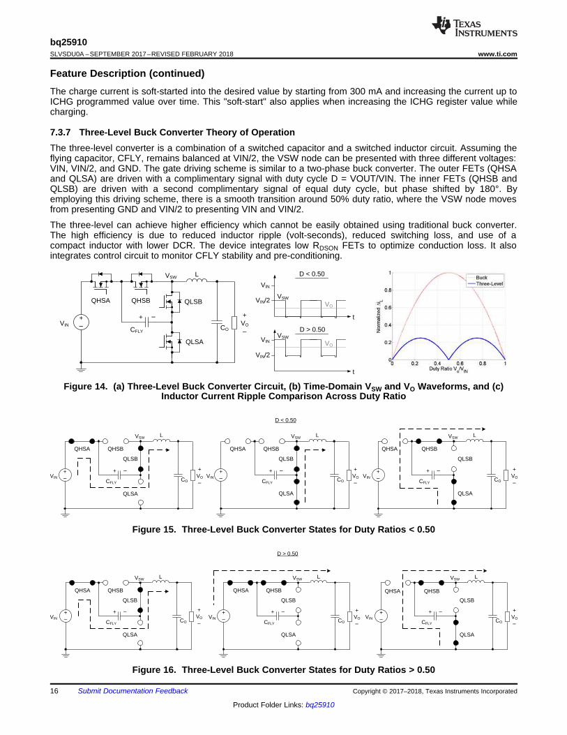
7.3.7 Three-Level Buck Converter Theory of OperationThe three-level converter is a combination of a switched capacitor and a switched inductor circuit. Assuming theflying capacitor, CFLY, remains balanced at VIN/2, the VSW node can be presented with three different voltages:VIN, VIN/2, and GND. The gate driving scheme is similar to a two-phase buck converter. The outer FETs (QHSAand QLSA) are driven with a complimentary signal with duty cycle D = VOUT/VIN. The inner FETs (QHSB andQLSB) are driven with a second complimentary signal of equal duty cycle, but phase shifted by 180°. Byemploying this driving scheme, there is a smooth transition around 50% duty ratio, where the VSW node movesfrom presenting GND and VIN/2 to presenting VIN and VIN/2.
The three-level can achieve higher efficiency which cannot be easily obtained using traditional buck converter.The high efficiency is due to reduced inductor ripple (volt-seconds), reduced switching loss, and use of acompact inductor with lower DCR. The device integrates low RDSON FETs to optimize conduction loss. It alsointegrates control circuit to monitor CFLY stability and pre-conditioning.
Figure 14. (a) Three-Level Buck Converter Circuit, (b) Time-Domain VSW and VO Waveforms, and (c)Inductor Current Ripple Comparison Across Duty Ratio
Figure 15. Three-Level Buck Converter States for Duty Ratios < 0.50
Figure 16. Three-Level Buck Converter States for Duty Ratios > 0.50

PORWatchdog timer expired
Reset registersI2C interface enabled
Host ModeStart Watchdog timer
Host programs registers
WD_RST bit = 1?
Watchdog Timer Expired?
Default ModeWatchdog timer expiredReset selective registers
WD_RST bit = 1?
N
Y
Y
N
N
Y
17
bq25910www.ti.com SLVSDU0A –SEPTEMBER 2017–REVISED FEBRUARY 2018
Product Folder Links: bq25910
Submit Documentation FeedbackCopyright © 2017–2018, Texas Instruments Incorporated
Feature Description (continued)7.3.8 Host Mode and Default Mode
7.3.8.1 Host Mode and Default Mode in bq25910The bq25910 is a host controlled charger, and will automatically shut off when the I2C watchdog timer is not resetwithin the timer period. In default (HIZ) mode, the device automatically disables charging until the host writes theEN_CHG bit high again and resets the watchdog timer via the WD_RST bit. When the charger is in defaultmode, WD_STAT bit is HIGH. When the charger is in host mode, WD_STAT bit is LOW.
After power-on-reset, the device starts in default mode with watchdog timer expired. All the registers are in thedefault settings. In default mode, the device remains in HIZ mode and will not charge the battery.
Writing a 1 to the WD_RST bit forces the charger out of default mode and into host mode. All the deviceparameters can be programmed by the host. To keep the device in host mode, the host has to reset thewatchdog timer by writing 1 to WD_RST bit before the watchdog timer expires (WD_STAT bit is set), or disablewatchdog timer by setting WATCHDOG bits = 00.
When the watchdog timer is expired (WD_STAT bit = 1), the device returns to default mode and registers arereset to default values except as detailed in the I2C register section. As long as the watchdog timer is expired(WD_STAT bit = 1), the device remains in Default Mode without charging the battery, regardless of the EN_CHGbit state. In order to enable charge after watchdog expired, write WD_RST = 1, and EN_CHG = 1.
Figure 17. Watchdog Timer Flow Chart
The REG_RST bit can be used to reset all of the registers (except STATUS registers) to their default value atany time.
7.3.9 Battery Charging ManagementThe device charges single-cell Li-Ion battery with up to 6-A charge current for high-capacity battery.
7.3.9.1 Autonomous Charging CycleWhen battery charging is enabled (EN_CHG bit = 1) and the battery is above VBAT_LOWV, the deviceautonomously completes a charging cycle. The device default charging parameters are listed in Table 1. Thehost can always control the charging operations and optimize the charging parameters by writing to thecorresponding registers through I2C.

18
bq25910SLVSDU0A –SEPTEMBER 2017–REVISED FEBRUARY 2018 www.ti.com
Product Folder Links: bq25910
Submit Documentation Feedback Copyright © 2017–2018, Texas Instruments Incorporated
Feature Description (continued)Table 1. Charging Parameter Default Settings
PARAMETER VALUEVBAT to start fast charge (VBATLOWV) 3.5 V
Charging voltage (VREG) 4.350 VCharging current (ICHG) 3.500 A
Termination current (ITERM) 1.000 ASafety timer (CHG_TIMER) 12 hours
A new charge cycle starts when the following conditions are valid:• Converter starts• Battery charging is enabled by EN_CHG bit, and ICHG register is not 0 mA• Battery voltage above VBAT_LOWV• No safety timer fault
The charger device automatically terminates the charging cycle when the charging current is below terminationthreshold, and device not in DPM mode or thermal regulation. Once termination is detected, an INT is assertedto the host and the EN_CHG bit gets reset to zero. After the charge is done, EN_CHG bit can initiate a newcharging cycle.
Once a charging cycle is complete, an INT pulse is asserted to notify the host. In addition the status register(CHRG_STAT) indicates the different charging phases (any change in CHRG_STAT will generate an INT tonotify the host):• 000: Charging disable• 001: Reserved• 010: Reserved• 011: Fast charge (constant current mode)• 100: Taper charge (constant voltage mode)• 101: Reserved• 110: Reserved• 111: Reserved
7.3.10 Master Charger and Parallel Charger InteractionsA master charger is required in the system to manage pre-charging and full termination of the battery. Thebq25910 monitors the battery voltage and compares it to VBAT_LOWV to ensure battery can safely take fast-chargecurrent. Once the bq25910 turns on and begins fast-charging, the host has two options: disable (HIZ) the mastercharger, or continue running the master charger along with the parallel charger.
For the first option, once battery voltage reaches VBAT_LOWV, the master charger maintains the BATFET on tosupply system from battery (EN_HIZ = 1 on master charger), and the bq25910 provides both the charge currentand system current if required. It is recommended to select VBAT_LOWV equal to minimum system voltage in orderto maintain system operation during transition. The bq25910 will then fast-charge the battery up to VREG andcontinue to regulate voltage while battery current tapers down. After the bq25910 detects termination, the hostcan re-enable the master charger to regulate battery voltage in CV mode down to lower termination currents.
The second mode of operation requires both chargers to stay on. In order to maximize efficiency, it isrecommended to run the master charger at lower charge current than the bq25910. For example, the mastercharger might be set at 1 A and the bq25910 at 3.5 A to achieve total charge current of 4.5 A. In this mode ofoperation, the master charger provides mostly system current, while the bq25910 provides mostly charge current.In this mode of operation, the bq25910 can select VBAT_LOWV as low as the battery dictates for fast-charge, sincethe master charger can maintain system voltage regulation and ensure system continues to operate through thetransition. After the bq25910 detects termination, the master charger automatically continues to regulate batteryvoltage in CV mode down to lower termination current.
Figure 18 shows both options with charge current for each device as well as battery voltage.

SYS_MIN
BATP - BATN
Master Charger ICHG
bq2591x ICHG
3.5V
4.35V
Master Charger:HIZ or,&+*���1A
bq25910:ICHG = 4.5A
Master Charger:HIZ or,&+*���1A
bq25910:ITERM = 1A
Master Charger:Pre-charges BAT
bq25910:Off
Master Charger:ITERM << 0.5A
bq25910:Off
Voltage
2A
4.5A
BATP - BATN
Time
CurrentTime
19
bq25910www.ti.com SLVSDU0A –SEPTEMBER 2017–REVISED FEBRUARY 2018
Product Folder Links: bq25910
Submit Documentation FeedbackCopyright © 2017–2018, Texas Instruments Incorporated
Figure 18. Master Charger and bq25910 Handoff
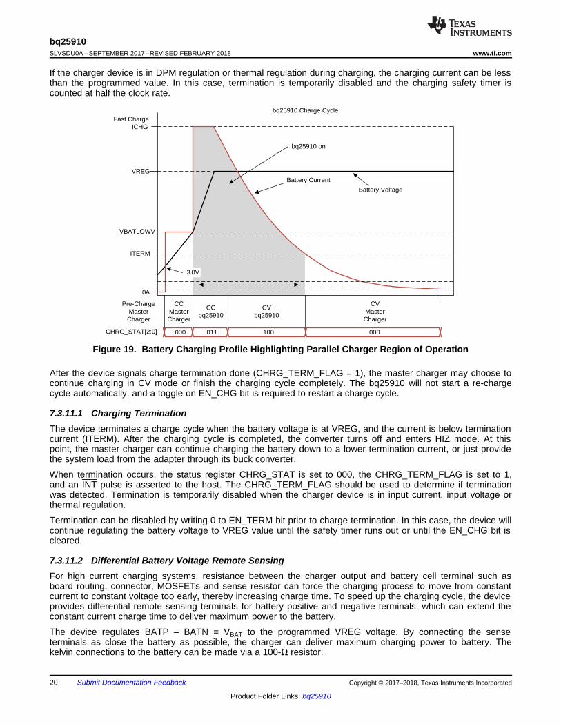
7.3.11 Battery Charging ProfileThe device charges the battery in two phases: constant current, and constant voltage. At the beginning of acharging cycle, the device checks the battery voltage and regulates current / voltage as needed. If the batteryvoltage is below VBAT_LOWV, it is the master charger responsibility to increase VBAT up to VBAT_LOWV so theparallel charger can initiate fast charging. As BAT increases to VBAT_LOWV, the master charger can stay in HIZand the bq25910 can start fast-charging the battery with up-to 6-A ICHG. Alternatively, the master charger canremain on to maintain the system load from adapter, while the bq25910 charges the battery. The default chargingsettings can be found in Table 2.
Table 2. Battery Charger SettingVBAT CHARGING CURRENT REG DEFAULT SETTING CHRG_STAT< 2 V Master controlled (IBATSHORT ) bq25910 off 000
2 V – VBAT_LOWV Master controlled (IPRECHG ) bq25910 off 000> VBAT_LOWV ICHG 3.500 A 011
VREG TAPER down to ITERM 4.350 V 100
Pre-ChargeMaster
Charger
Fast Charge
CCMasterCharger
Battery Current
Battery Voltage
bq25910 Charge Cycle
VBATLOWV
3.0V
ICHG
0A
ITERM
VREG
CHRG_STAT[2:0] 000 011 100 000
CCbq25910
CVbq25910
CVMaster
Charger
bq25910 on
20
bq25910SLVSDU0A –SEPTEMBER 2017–REVISED FEBRUARY 2018 www.ti.com
Product Folder Links: bq25910
Submit Documentation Feedback Copyright © 2017–2018, Texas Instruments Incorporated
If the charger device is in DPM regulation or thermal regulation during charging, the charging current can be lessthan the programmed value. In this case, termination is temporarily disabled and the charging safety timer iscounted at half the clock rate.
Figure 19. Battery Charging Profile Highlighting Parallel Charger Region of Operation
After the device signals charge termination done (CHRG_TERM_FLAG = 1), the master charger may choose tocontinue charging in CV mode or finish the charging cycle completely. The bq25910 will not start a re-chargecycle automatically, and a toggle on EN_CHG bit is required to restart a charge cycle.
7.3.11.1 Charging TerminationThe device terminates a charge cycle when the battery voltage is at VREG, and the current is below terminationcurrent (ITERM). After the charging cycle is completed, the converter turns off and enters HIZ mode. At thispoint, the master charger can continue charging the battery down to a lower termination current, or just providethe system load from the adapter through its buck converter.
When termination occurs, the status register CHRG_STAT is set to 000, the CHRG_TERM_FLAG is set to 1,and an INT pulse is asserted to the host. The CHRG_TERM_FLAG should be used to determine if terminationwas detected. Termination is temporarily disabled when the charger device is in input current, input voltage orthermal regulation.
Termination can be disabled by writing 0 to EN_TERM bit prior to charge termination. In this case, the device willcontinue regulating the battery voltage to VREG value until the safety timer runs out or until the EN_CHG bit iscleared.
7.3.11.2 Differential Battery Voltage Remote SensingFor high current charging systems, resistance between the charger output and battery cell terminal such asboard routing, connector, MOSFETs and sense resistor can force the charging process to move from constantcurrent to constant voltage too early, thereby increasing charge time. To speed up the charging cycle, the deviceprovides differential remote sensing terminals for battery positive and negative terminals, which can extend theconstant current charge time to deliver maximum power to the battery.
The device regulates BATP – BATN = VBAT to the programmed VREG voltage. By connecting the senseterminals as close the battery as possible, the charger can deliver maximum charging power to battery. Thekelvin connections to the battery can be made via a 100-Ω resistor.

21
bq25910www.ti.com SLVSDU0A –SEPTEMBER 2017–REVISED FEBRUARY 2018
Product Folder Links: bq25910
Submit Documentation FeedbackCopyright © 2017–2018, Texas Instruments Incorporated
7.3.11.3 Charging Safety TimerThe device has built-in safety timer to prevent extended charging cycle due to abnormal battery conditions. Theuser can program fast charge safety timer through I2C (CHG_TIMER bits). When safety timer expires, theTMR_FLAG bit is set to 1, and an INT pulse is asserted to the host. The safety timer feature can be disabled viaI2C using EN_TIMER bit.
During input voltage, current or thermal regulation, the safety timer counts at half clock rate as the actual chargecurrent is likely to be below the register setting. For example, if the charger is in input current regulation(IINDPM_STAT = 1) throughout the whole charging cycle, and the safety timer is set to 5 hours, then the timerwill expire in 10 hours. This half clock rate feature can be disabled by setting TMR2X_EN = 0. Changing theTMR2X_EN bit while the device is running has no effect on the safety timer count, other than forcing the timer tocount at half the rate under the conditions dictated above.
7.4 Device Functional Modes
7.4.1 Lossless Current SensingIn high current charging systems, extra resistance between the charger output and the battery contribute topower loss and temperature rise. The bq25910 regulates the output current without the need of a sense resistor,thereby reducing system power loss and operating temperature. Switching FET current information is used inconjunction to inductor DCR sensing to regulate output current accurately. For optimal operation, the voltagedrop across the DCR should be below 180 mV. For example, to achieve 6-A charging, the DCR should be below30 mΩ. In addition to lossless current regulation, the switching FET current is monitored on a cycle-by-cyclebasis to ensure safe operation.
7.4.2 Dynamic Power ManagementTo meet maximum current limit in USB spec and avoid over-loading the adapter, the device features DynamicPower Management (DPM), which continuously monitors the input current and input voltage. When input sourceis over-loaded, either the current exceeds the input current limit (IINDPM) or the voltage falls below the inputvoltage limit (VINDPM). The device then reduces the charge current until the input current falls below the inputcurrent limit and the input voltage rises above the input voltage limit.
During DPM mode, the status register bits VINDPM_STAT (VINDPM) and/or IINDPM_STAT (IINDPM) is/are setto 1. Figure 20 shows the IINDPM response with 9-V/1.33-A (12-W) adapter, 4.0-V battery, 3.5-A charge current,and bq25910 in CV mode.

8.5V
9.0V
4A
2A
0A
3A
1A
-1A
VBUS
IBUS
IBAT
IOUT
ISYS
CV IINDPM CV
bq25898 (Hi-Z Mode)
bq25910
VBUS SYS
BAT
SW2
GND
VBUS
VBAT
+
-
SYSTEM LOAD
ISYS
IOUT,910
IBAT
IBUS
VBUS
22
bq25910SLVSDU0A –SEPTEMBER 2017–REVISED FEBRUARY 2018 www.ti.com
Product Folder Links: bq25910
Submit Documentation Feedback Copyright © 2017–2018, Texas Instruments Incorporated
Device Functional Modes (continued)
Figure 20. DPM Response
7.4.3 Interrupt to Host (INT)In some applications, the host does not always monitor the charger operation. The INT pin notifies the systemhost on the device operation. By default, the following events will generate an active-low, 256-μs INT pulse.1. Good input source detected (three conditions below met)
– VVBUS > VBAT (not in sleep)– VVBUS < VVBUS_OV– VVBUS > VVPOORSRC (typ 3.7 V) when IPOORSRC (typ 20 mA) current is applied (not a poor source)
2. Good input source removed3. POORSRC routine failed 7 consecutive times (connected adaptor was found to be a poor source)4. Capacitor pre-charge routine failed (CFLY / CAUX failed to pre-charge)5. Entering IINDPM regulation6. Entering VINDPM regulation7. Entering device Junction Temperature Regulation

INT
I2C Flag Read
IINDPM_FLAG
IINDPM_STAT
TREG_FLAG
TREG_STAT
23
bq25910www.ti.com SLVSDU0A –SEPTEMBER 2017–REVISED FEBRUARY 2018
Product Folder Links: bq25910
Submit Documentation FeedbackCopyright © 2017–2018, Texas Instruments Incorporated
Device Functional Modes (continued)8. I2C Watchdog timer expired
– At initial power-up, this INT gets asserted to signal I2C is ready for communication9. Charger changes state (CHRG_STAT value change)10. VBUS over-voltage detected11. Junction temperature shutdown (TSHUT)12. Battery over-voltage detected (BATOVP)13. CFLY fault detected14. Charge Safety Timer Expired
Each one of these INT sources can be masked off to prevent INT pulses from being sent out when they occur.Three bits exist for each one of these events:• The STAT bit holds the current status of each INT source• The FLAG bit holds information on which source produced an INT, regardless of current status.• The MASK bit is used to prevent the device from sending out INT for each particular event.
When one of the above conditions occurs, the device sends out an INT pulse and keeps track of which sourcegenerated the INT via the FLAG registers. The FLAG register bits are automatically reset to zero after the hostreads them, and a new edge on STAT bit is required to re-assert the FLAG.
Figure 21. INT Generation Behavior Example
7.4.4 Protections
7.4.4.1 Voltage and Current MonitoringThe device closely monitors the input and output voltage, as well as switching FET currents for safe buck modeoperation.

24
bq25910SLVSDU0A –SEPTEMBER 2017–REVISED FEBRUARY 2018 www.ti.com
Product Folder Links: bq25910
Submit Documentation Feedback Copyright © 2017–2018, Texas Instruments Incorporated
Device Functional Modes (continued)7.4.4.1.1 Input Over-Voltage (VVBUS_OV)
The valid input voltage range for buck mode operation is VVBUS_OP. If VBUS voltage exceeds VVBUS_OV, thedevice stops switching immediately to protect the power FETs. During input over-voltage, an INT pulse isasserted to signal the host, and the VBUS_OVP_STAT and VBUS_OVP_FLAG fault register bits get set. Thedevice automatically starts switching again when the over-voltage condition goes away.
7.4.4.1.2 Input Under-Voltage (VPOORSRC)
The valid input voltage range for buck mode operation is VVBUS_OP. If VBUS voltage falls below VPOORSRC, thedevice stops switching. During input under-voltage, an INT pulse is asserted to signal the host, and thePG_STAT bit gets cleared. The PG_FLAG bit will get set to signal this event. The device automatically attemptsto restart switching when the under-voltage condition goes away.
7.4.4.1.3 Flying Capacitor Over- or Under-Voltage Protection (VCFLY_OVP and VCFLY_UVP)
Under normal operating conditions the flying capacitor is balanced by the converter. However, during linetransients or other failures, capacitor mis-balance is possible. The device constantly monitors the flying capacitorvoltage. If VCFLY exceeds the protection limits, the device stops switching immediately. When this fault isdetected, an INT pulse is asserted to notify the host, and the CFLY_STAT and CFLY_FLAG fault register bits getset. The device automatically attempts to re-balance the cap and resumes charging if successful. If the devicefails to re-balance CFLY, the CAP_COND_STAT and CAP_COND_FLAG fault register bits get set, and anEN_CHG toggle is required to re-attempt charging.
7.4.4.1.4 Over Current Protection
The device monitors the outer switching FET current on a cycle-by-cycle basis . If an over-current is detected,the device responds by forcing the switching FETs to immediately discharge the inductor current and attemptcurrent ramp-up once again.
7.4.4.2 Thermal Regulation and Thermal ShutdownThe device monitors internal junction temperature TJ to avoid overheating the chip and limits the device surfacetemperature in buck mode. When the internal junction temperature exceeds the preset thermal regulation limit(TREG bits), the device reduces charge current. A wide thermal regulation range from 60°C to 120°C allows theuser to optimize the system thermal performance.
During thermal regulation, the actual charging current is usually below the programmed value in ICHG registers.Therefore, termination is disabled, the safety timer runs at half the clock rate, the status register TREG_STAT bitgoes high, and an INT is asserted to the host.
Additionally, the device has thermal shutdown to turn off the converter when device surface temperature exceedsTSHUT. The fault register TSHUT_STAT is set and an INT pulse is asserted to the host. The converter turns backon when device temperature is below TSHUT_HYS.
7.4.4.3 Battery Protection
7.4.4.3.1 Battery Over-Voltage Protection (BATOVP)
The battery over-voltage limit is clamped at 4% above the battery regulation voltage. When battery over-voltageoccurs, the charger device immediately disables charge. The fault register BATOVP_STAT bit goes high and anINT pulse is asserted to signal the host.
7.5 Programming
7.5.1 Serial InterfaceThe device uses I2C compatible interface for flexible charging parameter programming and instantaneous devicestatus reporting. I2C is a bi-directional 2-wire serial interface. Only two open-drain bus lines are required: a serialdata line (SDA), and a serial clock line (SCL). Devices can be considered as masters or slaves when performingdata transfers. A master is a device which initiates a data transfer on the bus and generates the clock signals topermit that transfer. At that time, any device addressed is considered a slave.

START (S) STOP (P)
SDA
SCL
SDA
SCL
SDA
SCL
Data line stable; Data valid Change of
data allowed
25
bq25910www.ti.com SLVSDU0A –SEPTEMBER 2017–REVISED FEBRUARY 2018
Product Folder Links: bq25910
Submit Documentation FeedbackCopyright © 2017–2018, Texas Instruments Incorporated
Programming (continued)The device operates as a slave device with address 4BH, receiving control inputs from the master device likemicro-controller or digital signal processor through REG00-REG0D. Register read beyond REG0D (0x0D) returns0xFF. The I2C interface supports both standard mode (up to 100 kbits/s), and fast mode (up to 400 kbits/s).When the bus is free, both lines are HIGH. The SDA and SCL pins are open drain and must be connected to thepositive supply voltage via a current source or pull-up resistor.
7.5.2 Data ValidityThe data on the SDA line must be stable during the HIGH period of the clock. The HIGH or LOW state of thedata line can only change when the clock signal on SCL line is LOW. One clock pulse is generated for each databit transferred.
Figure 22. Bit Transfers on the I2C Bus
7.5.3 START and STOP ConditionsAll transactions begin with a START (S) and are terminated with a STOP (P). A HIGH to LOW transition on theSDA line while SCL is HIGH defines a START condition. A LOW to HIGH transition on the SDA line when theSCL is HIGH defines a STOP condition. START and STOP conditions are always generated by the master. Thebus is considered busy after the START condition, and free after the STOP condition.
Figure 23. START and STOP Conditions on the I2C Bus
7.5.4 Byte FormatEvery byte on the SDA line must be 8 bits long. The number of bytes to be transmitted per transfer isunrestricted. Each byte has to be followed by an ACKNOWLEDGE (ACK) bit. Data is transferred with the MostSignificant Bit (MSB) first. If a slave cannot receive or transmit another complete byte of data until it hasperformed some other function, it can hold the SCL line low to force the master into a wait state (clockstretching). Data transfer then continues when the slave is ready for another byte of data and releases the SCLline.

SCL
SDA
START
S 1-7 8 9
ACK
1-7 8 9
ACK
1-7 8 9
STOP
P
ADDRESS R/W DATA ACKDATA
Slave Address
R / W1 0 0 1 0 1 1
SCL
SDA
START or Repeated START
S or Sr 1 2 7 8 9
MSB
ACK
Acknowledgement signal from slave
1 2 8 9
ACK
Acknowledgement signal from receiver
STOP or Repeated START
P or Sr
26
bq25910SLVSDU0A –SEPTEMBER 2017–REVISED FEBRUARY 2018 www.ti.com
Product Folder Links: bq25910
Submit Documentation Feedback Copyright © 2017–2018, Texas Instruments Incorporated
Programming (continued)
Figure 24. Data Transfer on the I2C Bus
7.5.5 Acknowledge (ACK) and Not Acknowledge (NACK)The ACK signaling takes place after byte. The ACK bit allows the receiver to signal the transmitter that the bytewas successfully received and another byte may be sent. All clock pulses, including the acknowledge 9th clockpulse, are generated by the master. The transmitter releases the SDA line during the acknowledge clock pulseso the receiver can pull the SDA line LOW and it remains stable LOW during the HIGH period of this 9th clockpulse. A NACK is signaled when the SDA line remains HIGH during the 9th clock pulse. The master can thengenerate either a STOP to abort the transfer or a repeated START to start a new transfer.
7.5.6 Slave Address and Data Direction BitAfter the START signal, a slave address is sent. This address is 7 bits long, followed by the 8 bit as a datadirection bit (bit R/W). A zero indicates a transmission (WRITE) and a one indicates a request for data (READ).The device 7-bit address is defined as 1001 011’ (0x4BH) by default. The address bit arrangement for 4BH isshown in Figure 25.
Figure 25. 14: 7-Bit Addressing (4BH)
Figure 26. Complete Data Transfer on I2C Bus
7.5.7 Single Read and Write
Figure 27. Single Write

27
bq25910www.ti.com SLVSDU0A –SEPTEMBER 2017–REVISED FEBRUARY 2018
Product Folder Links: bq25910
Submit Documentation FeedbackCopyright © 2017–2018, Texas Instruments Incorporated
Programming (continued)
Figure 28. Single Read
If the register address is not defined, the charger device sends back NACK and returns to the idle state.
7.5.8 Multi-Read and Multi-WriteThe charger device supports multi-read and multi-write of all registers.
Figure 29. Multi-Write
Figure 30. Multi-Read

28
bq25910SLVSDU0A –SEPTEMBER 2017–REVISED FEBRUARY 2018 www.ti.com
Product Folder Links: bq25910
Submit Documentation Feedback Copyright © 2017–2018, Texas Instruments Incorporated
7.6 Register Maps
7.6.1 I2C RegistersTable 3 lists the memory-mapped registers for the I2C. All register offset addresses not listed in Table 3 shouldbe considered as reserved locations and the register contents should not be modified.
Table 3. I2C Register Summary TableAddress Access Type Acronym Register Name Section
0h R/W REG00 Battery Voltage Limit Go1h R/W REG01 Charge Current Limit Go2h R/W REG02 Input Voltage Limit Go3h R/W REG03 Input Current Limit Go4h R/W REG04 RESERVED Go5h R/W REG05 Charger Control 1 Go6h R/W REG06 Charger Control 2 Go7h R REG07 INT Status Go8h R REG08 FAULT Status Go9h R REG09 INT Flag GoAh R REG0A FAULT Flag GoBh R/W REG0h INT Mask GoCh R/W REG0C FAULT Mask GoDh R/W REG0D Part Information Go
Complex bit access types are encoded to fit into small table cells. Table 4 shows the codes that are used foraccess types in this section.
Table 4. I2C Access Type CodesAccess Type Code DescriptionRead TypeR R ReadWrite TypeW W WriteReset Value-n Value after reset-X Undefined value

29
bq25910www.ti.com SLVSDU0A –SEPTEMBER 2017–REVISED FEBRUARY 2018
Product Folder Links: bq25910
Submit Documentation FeedbackCopyright © 2017–2018, Texas Instruments Incorporated
7.6.1.1 Battery Voltage Regulation Limit Register (Address = 0h) [reset = AAh]REG00 is shown in Figure 31 and described in Table 5.
Return to Summary Table.
Figure 31. REG00 Register
7 6 5 4 3 2 1 0VREG[7:0]R/W-AAh
Table 5. REG00 Register Field Descriptions
Bit Field Type Reset byREG_RST
Reset byWATCHDOG Description
7 VREG[7] R/W Yes Yes 640 mV Charge voltage limit:Offset: 3.5 VRange: 3.5 V to 4.775 VDefault 4.35 V
6 VREG[6] R/W Yes Yes 320 mV
5 VREG[5] R/W Yes Yes 160 mV
4 VREG[4] R/W Yes Yes 80 mV
3 VREG[3] R/W Yes Yes 40 mV
2 VREG[2] R/W Yes Yes 20 mV
1 VREG[1] R/W Yes Yes 10 mV
0 VREG[0] R/W Yes Yes 5 mV

30
bq25910SLVSDU0A –SEPTEMBER 2017–REVISED FEBRUARY 2018 www.ti.com
Product Folder Links: bq25910
Submit Documentation Feedback Copyright © 2017–2018, Texas Instruments Incorporated
7.6.1.2 Charger Current Limit Register (Address = 1h) [reset = 46h]REG01 is shown in Figure 32 and described in Table 6.
Return to Summary Table.
Figure 32. REG01 Register
7 6 5 4 3 2 1 0RESERVED ICHG[6:0]
R/W-0h R/W-46h
Table 6. REG01 Register Field Descriptions
Bit Field Type Reset byREG_RST
Reset byWATCHDOG Description
7 RESERVED R/W Yes Yes Reserved bit always reads 0h6 ICHG[6] R/W Yes Yes 3200 mA Fast charge current limit
Offset: 0 mARange: 0 mA to 6000 mADefault: 3500 mANOTE: ICHG > 6 A (78h) clamped to 6 AICHG < 300 mA (06h) clamped to 0 A
5 ICHG[5] R/W Yes Yes 1600 mA
4 ICHG[4] R/W Yes Yes 800 mA
3 ICHG[3] R/W Yes Yes 400 mA
2 ICHG[2] R/W Yes Yes 200 mA
1 ICHG[1] R/W Yes Yes 100 mA
0 ICHG[0] R/W Yes Yes 50 mA

31
bq25910www.ti.com SLVSDU0A –SEPTEMBER 2017–REVISED FEBRUARY 2018
Product Folder Links: bq25910
Submit Documentation FeedbackCopyright © 2017–2018, Texas Instruments Incorporated
7.6.1.3 Input Voltage Limit Register (Address = 2h) [reset = 04h]REG02 is shown in Figure 33 and described in Table 7.
Return to Summary Table.
Figure 33. REG02 Register
7 6 5 4 3 2 1 0RESERVED VINDPM[6:0]
R/W-0h R/W-04h
Table 7. REG02 Register Field Descriptions
Bit Field Type Reset byREG_RST
Reset byWATCHDOG Description
7 RESERVED R/W Yes No Reserved bit always reads 0h6 VINDPM[6] R/W Yes No 6400 mV Absolute input-voltage limit
Offset: 3.9 VRange: 3.9 V to 14 VDefault: 4.3 VNOTE: VINDPM > 14 V (65h) clamped to 14 V
5 VINDPM[5] R/W Yes No 3200 mV
4 VINDPM[4] R/W Yes No 1600 mV
3 VINDPM[3] R/W Yes No 800 mV
2 VINDPM[2] R/W Yes No 400 mV
1 VINDPM[1] R/W Yes No 200 mV
0 VINDPM[0] R/W Yes No 100 mV

32
bq25910SLVSDU0A –SEPTEMBER 2017–REVISED FEBRUARY 2018 www.ti.com
Product Folder Links: bq25910
Submit Documentation Feedback Copyright © 2017–2018, Texas Instruments Incorporated
7.6.1.4 Input Current Limit Register (Address = 3h) [reset = 13h]REG03 is shown in Figure 34 and described in Table 8.
Return to Summary Table.
Figure 34. REG03 Register
7 6 5 4 3 2 1 0RESERVED INDPM[5:0]
R/W-0h R/W-13h
Table 8. REG03 Register Field Descriptions
Bit Field Type Reset byREG_RST
Reset byWATCHDOG Description
7-6 RESERVED R/W Yes No Reserved bit always reads 0h5 INDPM[5] R/W Yes No 3200 mA Input current limit
Offset: 500 mARange: 500 mA to 3600 mADefault: 2400 mANOTE: INDPM > 3600 mA (1Fh) clamped to 3600mA
4 INDPM[4] R/W Yes No 1600 mA
3 INDPM[3] R/W Yes No 800 mA
2 INDPM[2] R/W Yes No 400 mA
1 INDPM[1] R/W Yes No 200 mA
0 INDPM[0] R/W Yes No 100 mA
33
bq25910www.ti.com SLVSDU0A –SEPTEMBER 2017–REVISED FEBRUARY 2018
Product Folder Links: bq25910
Submit Documentation FeedbackCopyright © 2017–2018, Texas Instruments Incorporated
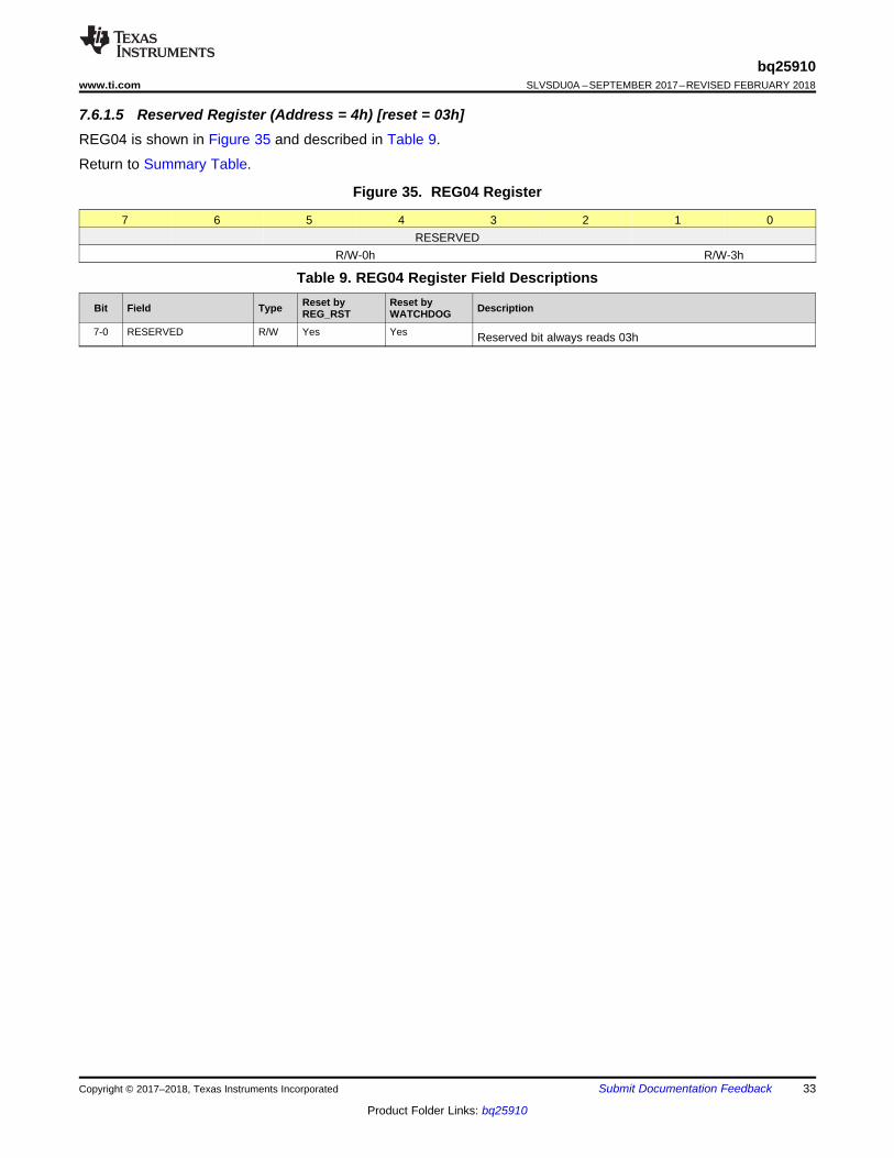
7.6.1.5 Reserved Register (Address = 4h) [reset = 03h]REG04 is shown in Figure 35 and described in Table 9.
Return to Summary Table.
Figure 35. REG04 Register
7 6 5 4 3 2 1 0RESERVED
R/W-0h R/W-3h
Table 9. REG04 Register Field Descriptions
Bit Field Type Reset byREG_RST
Reset byWATCHDOG Description
7-0 RESERVED R/W Yes Yes Reserved bit always reads 03h

34
bq25910SLVSDU0A –SEPTEMBER 2017–REVISED FEBRUARY 2018 www.ti.com
Product Folder Links: bq25910
Submit Documentation Feedback Copyright © 2017–2018, Texas Instruments Incorporated
7.6.1.6 Charger Control 1 Register (Address = 5h) [reset = 9Dh]REG05 is shown in Figure 36 and described in Table 10.
Return to Summary Table.
When the WATCHDOG[1:0] bits change (writing the same value does not change these bits), the internalcounter is reset. The same applies for the CHG_TIMER bits (changing the value in the register will reset theCHG_TIMER).
Figure 36. REG05 Register
7 6 5 4 3 2 1 0EN_TERM WD_RST WATCHDOG[1:0] EN_TIMER CHG_TIMER[1:0] TMR2X_EN
R/W-1h R/W-0h R/W-1h R/W-1h R/W-2h R/W-1h
Table 10. REG05 Register Field Descriptions
Bit Field Type Reset byREG_RST
Reset byWATCHDOG Description
7 EN_TERM R/W Yes Yes Termination control0h = Disable termination1h = Enable termination
6 WD_RST R/W Yes Yes I2C watchdog-timer reset0h = Normal1h = Reset (bit returns to 0 after time reset)
5-4 WATCHDOG[1:0] R/W Yes Yes I2C watchdog-timer settings0h = Disable watchdog timer1h = 40 s2h = 80 s3h = 160 s
3 EN_TIMER R/W Yes Yes Charging safety-timer enable0h = Disable1h = Enable
2-1 CHG_TIMER[1:0] R/W Yes Yes Fast-charge safety timer setting0h = 5 hours1h = 8 hours2h = 12 hours3h = 20 hours
0 TMR2X_EN R/W Yes Yes Safety timer behavior during DPM or TREG0h = Safety timer always counts normally1h = Safety timer count slowed by 2x during input DPM orTREG

35
bq25910www.ti.com SLVSDU0A –SEPTEMBER 2017–REVISED FEBRUARY 2018
Product Folder Links: bq25910
Submit Documentation FeedbackCopyright © 2017–2018, Texas Instruments Incorporated
7.6.1.7 Charger Control 2 Register (Address = 6h) [reset = 33h]REG06 is shown in Figure 37 and described in Table 11.
Return to Summary Table.
When the watchdog timer expires (WD_STAT = 1h), the EN_CHG bit is held in reset. To enable the charger afterthe watchdog expires, write a value of 1h to the WD_RST bit and a value of 1h to the EN_CHG bit.
Figure 37. REG06 Register
7 6 5 4 3 2 1 0RESERVED TREG[1:0] EN_CHG RESERVED VBATLOWV[1:0]
R/W-0h R/W-3h R/W-0h R/W-0h R/W-3h
Table 11. REG06 Register Field Descriptions
Bit Field Type Reset byREG_RST
Reset byWATCHDOG Description
7-6 RESERVED R/W Yes Yes Reserved bit always reads 0h5-4 TREG[1:0] R/W Yes Yes Thermal regulation threshold
0h = 60°C1h = 80°C2h = 100°C3h = 120°C
3 EN_CHG R/W Yes Yes Charger enable configuration0h = Charger disabled1h = Charger enabled
2 RESERVED R/W Yes Yes Reserved bit always reads 0h1-0 VBATLOWV[1:0] R/W Yes No VBAT_LOWV threshold to start charging at ICHG programmed
setting:0h = 2.6 V1h = 2.9 V2h = 3.2 V3h = 3.5 V

36
bq25910SLVSDU0A –SEPTEMBER 2017–REVISED FEBRUARY 2018 www.ti.com
Product Folder Links: bq25910
Submit Documentation Feedback Copyright © 2017–2018, Texas Instruments Incorporated
7.6.1.8 INT Status Register (Address = 7h) [reset = X]REG07 is shown in Figure 38 and described in Table 12.
Return to Summary Table.
Figure 38. REG07 Register
7 6 5 4 3 2 1 0PG_STAT INDPM_STAT VINDPM_STAT TREG_STAT WD_STAT CHRG_STAT[2:0]
R-X R-X R-X R-X R-X R-X
Table 12. REG07 Register Field Descriptions
Bit Field Type Reset byREG_RST
Reset byWATCHDOG Description
7 PG_STAT R Yes Yes Power-good status0h = Not power good1h = Power good
6 INDPM_STAT R Yes Yes INDPM status0h = Normal1h = In INDPM regulation
5 VINDPM_STAT R Yes Yes VINDPM status0h = Normal1h = In VINDPM regulation
4 TREG_STAT R Yes Yes Device thermal-regulation status0h = Normal1h = In thermal regulation
3 WD_STAT R Yes No I2C watchdog-timer status0h = Normal1h = Watchdog timer expired
2-0 CHRG_STAT[2:0] R Yes Yes Charge status0h = Not charging1h = Reserved2h = Reserved3h = Fast charging (CC mode)4h = Taper charging (CV mode)5h = Reserved6h = Reserved7h = Reserved

37
bq25910www.ti.com SLVSDU0A –SEPTEMBER 2017–REVISED FEBRUARY 2018
Product Folder Links: bq25910
Submit Documentation FeedbackCopyright © 2017–2018, Texas Instruments Incorporated
7.6.1.9 FAULT Status Register (Address = 8h) [reset = X]REG08 is shown in Figure 39 and described in Table 13.
Return to Summary Table.
When the watchdog timer expires (WD_STAT = 1h), the VBUS_OVP_STAT, TSHUT_STAT, BATOVP_STAT,and CFLY_STAT bits are held in reset until the watchdog fault is cleared (WD_RST bit = 1h, or changing theWATCHDOG[1:0] bits).
Figure 39. REG08 Register
7 6 5 4 3 2 1 0VBUS_OVP_S
TATTSHUT_STAT BATOVP_STA
TCFLY_STAT RESERVED CAP_COND_S
TATPOORSRC_ST
ATRESERVED
R-X R-X R-X R-X R-0h R-X R-X R-0h
Table 13. REG08 Register Field Descriptions
Bit Field Type Reset byREG_RST
Reset byWATCHDOG Description
7 VBUS_OVP_STAT R Yes Yes Input-overvoltage status0h = Normal1h = Device in overvoltage protection
6 TSHUT_STAT R Yes Yes Device temperature-shutdown status0h = Normal1h = Device in thermal-shutdown protection
5 BATOVP_STAT R Yes Yes Battery overvoltage status0h = Normal1h = BATOVP (VBAT > VBATOVP)
4 CFLY_STAT R Yes Yes Flying capacitor status0h = Normal1h = Flying capacitor fault (VCFLY_UVP or OVP)
3 Reserved R Yes Yes Reserved bit always reads 0
2 CAP_COND_STAT R Yes Yes Capacitor precondition status0h = Normal1h = CFLY or CAUX precondition failed
1 POORSRC_STAT R Yes Yes Poor-source-detection status0h = Normal1h = POORSRC routine failed 7 consecutive times
0 RESERVED R Yes Yes Reserved bit always reads 0

38
bq25910SLVSDU0A –SEPTEMBER 2017–REVISED FEBRUARY 2018 www.ti.com
Product Folder Links: bq25910
Submit Documentation Feedback Copyright © 2017–2018, Texas Instruments Incorporated
7.6.1.10 INT Flag Status Register (Address = 9h) [reset = 00h]REG09 is shown in Figure 40 and described in Table 14.
Return to Summary Table.
All bits in REG09 are automatically cleared after a read.
Figure 40. REG09 Register
7 6 5 4 3 2 1 0PG_FLAG INDPM_FLAG VINDPM_FLAG TREG_FLAG WD_FLAG CHRG_TERM_
FLAGRESERVED CHRG_FLAG
R-0h R-0h R-0h R-0h R-0h R-0h R-0h R-0h
Table 14. REG09 Register Field Descriptions
Bit Field Type Reset byREG_RST
Reset byWATCHDOG Description
7 PG_FLAG R Yes No Power-good INT flag0h = Normal1h = PG-signal toggle detected
6 INDPM_FLAG R Yes No INDPM-regulation INT flag0h = Normal1h = INDPM-signal rising edge detected
5 VINDPM_FLAG R Yes No VINDPM-regulation INT flag0h = Normal1h = VINDPM-signal rising edge detected
4 TREG_FLAG R Yes No Device temperature-regulation INT flag0h = Normal1h = TREG-signal rising edge detected
3 WD_FLAG R Yes No I2C-watchdog INT flag0h = Normal1h = WD_STAT-signal rising edge detected
2 CHRG_TERM_FLAG R Yes No Charger-termination INT flag0h = Normal1h = Charger-termination signal rising edge detected
1 RESERVED R Yes No Reserved bit always reads 00 CHRG_FLAG R Yes No Charger status INT flag
0h = Normal1h = CHRG_STAT[2:0] bits changed (transition to any state)

39
bq25910www.ti.com SLVSDU0A –SEPTEMBER 2017–REVISED FEBRUARY 2018
Product Folder Links: bq25910
Submit Documentation FeedbackCopyright © 2017–2018, Texas Instruments Incorporated
7.6.1.11 FAULT Flag Register (Address = Ah) [reset = 00h]REG0A is shown in Figure 41 and described in Table 15.
Return to Summary Table.
All bits in REG0A are automatically cleared after a read.
Figure 41. REG0A Register
7 6 5 4 3 2 1 0VBUS_OVP_FL
AGTSHUT_FLAG BATOVP_FLA
GCFLY_FLAG TMR_FLAG CAP_COND_F
LAGPOORSRC_FL
AGRESERVED
R-0h R-0h R-0h R-0h R-0h R-0h R-0h R-0h
Table 15. REG0A Register Field Descriptions
Bit Field Type Reset byREG_RST
Reset byWATCHDOG Description
7 VBUS_OVP_FLAG R Yes No Input-overvoltage INT flag0h = Normal1h = VBUS_OVP signal rising edge detected
6 TSHUT_FLAG R Yes No Thermal-shutdown INT flag0h = Normal1h = TSHUT signal rising edge detected
5 BATOVP_FLAG R Yes No Battery-overvoltage INT flag0h = Normal1h = BATOVP signal rising edge detected
4 CFLY_FLAG R Yes No Flying capacitor fault INT flag0h = Normal1h = Flying capacitor fault signal rising edge detected
3 TMR_FLAG R Yes No Charger safety-timer fault INT flag0h = Normal1h = Charger safety-timer expired rising edge
2 CAP_COND_FLAG R Yes No Capacitor precondition fault INT flag0h = Normal1h = CAP_COND_STAT signal rising edge detected
1 POORSRC_FLAG R Yes No Poor-source-fault INT flag0h = Normal1h = POORSRC_STAT signal rising edge detected
0 RESERVED R Yes No Reserved bit always reads 0

40
bq25910SLVSDU0A –SEPTEMBER 2017–REVISED FEBRUARY 2018 www.ti.com
Product Folder Links: bq25910
Submit Documentation Feedback Copyright © 2017–2018, Texas Instruments Incorporated
7.6.1.12 INT Mask Register (Address = Bh) [reset = 00h]REG0h is shown in Figure 42 and described in Table 16.
Return to Summary Table.
Figure 42. REG0h Register
7 6 5 4 3 2 1 0PG_MASK INDPM_MASK VINDPM_MAS
KTREG_MASK WD_MASK CHRG_TERM_
MASKRESERVED CHRG_MASK
R/W-0h R/W-0h R/W-0h R/W-0h R/W-0h R/W-0h R/W-0h R/W-0h
Table 16. REG0h Register Field Descriptions
Bit Field Type Reset byREG_RST
Reset byWATCHDOG Description
7 PG_MASK R/W Yes No Power-good INT mask0h = PG toggle produces INT pulse1h = PG toggle does not produce INT pulse
6 INDPM_MASK R/W Yes No INDPM-regulation INT mask0h = INDPM entry produces INT pulse1h = INDPM entry does not produce INT pulse
5 VINDPM_MASK R/W Yes No VINDPM-regulation INT mask0h = VINDPM entry produces INT pulse1h = VINDPM entry does not produce INT pulse
4 TREG_MASK R/W Yes No Device temperature-regulation INT mask0h = TREG entry produces INT pulse1h = TREG entry does not produce INT pulse
3 WD_MASK R/W Yes No I2C watchdog-timer INT mask0h = WD_STAT rising edge produces INT pulse1h = WD_STAT rising edge does not produce INT pulse
2 CHRG_TERM_MASK R/W Yes No Charger-termination INT mask0h = CHRG-termination detection produces INT pulse1h = CHRG-termination detection does not produce INT pulse
1 RESERVED R/W Yes No Reserved bit always reads 00 CHRG_MASK R/W Yes No Charger-status INT mask
0h = CHRG_STAT[2:0] bit change produces INT pulse1h = CHRG_STAT[2:0] bit change does not produce INT pulse

41
bq25910www.ti.com SLVSDU0A –SEPTEMBER 2017–REVISED FEBRUARY 2018
Product Folder Links: bq25910
Submit Documentation FeedbackCopyright © 2017–2018, Texas Instruments Incorporated
7.6.1.13 FAULT Mask Register (Address = Ch) [reset = 00h]REG0C is shown in Figure 43 and described in Table 17.
Return to Summary Table.
Figure 43. REG0C Register
7 6 5 4 3 2 1 0VBUS_OVP_M
ASKTSHUT_MASK BATOVP_MAS
KCFLY_MASK TMR_MASK CAP_COND_M
ASKPOORSRC_MA
SKRESERVED
R/W-0h R/W-0h R/W-0h R/W-0h R/W-0h R/W-0h R/W-0h R/W-0h
Table 17. REG0C Register Field Descriptions
Bit Field Type Reset byREG_RST
Reset byWATCHDOG Description
7 VBUS_OVP_MASK R/W Yes No Input overvoltage INT mask0h = VBUS_OVP rising edge produces INT pulse1h = VBUS_OVP rising edge does not produce INT pulse
6 TSHUT_MASK R/W Yes No Thermal-shutdown INT mask0h = TSHUT rising edge produces INT pulse1h = TSHUT rising edge does not produce INT pulse
5 BATOVP_MASK R/W Yes No Battery-overvoltage INT mask0h = BATOVP rising edge produces INT pulse1h = BATOVP rising edge does not produce INT pulse
4 CFLY_MASK R/W Yes No Flying capacitor fault INT mask0h = CFLY-fault rising edge produces INT pulse1h = CFLY-fault rising edge does not produce INT pulse
3 TMR_MASK R/W Yes No Charger safety-timer fault INT mask0h = Timer expired rising edge produces INT pulse1h = Timer expired rising edge does not produce INT pulse
2 CAP_COND_MASK R/W Yes No Capacitor precondition-fault INT mask0h = CAP_COND_FLAG rising edge produces INT pulse1h = CAP_COND_FLAG rising edge does not produce INTpulse
1 POORSRC_MASK R/W Yes No Poor-source-fault INT mask0h = POORSRC_FLAG rising edge produces INT pulse1h = POORSRC_FLAG rising edge does not produce INT pulse
0 RESERVED R/W Yes No Reserved bit always reads 0

42
bq25910SLVSDU0A –SEPTEMBER 2017–REVISED FEBRUARY 2018 www.ti.com
Product Folder Links: bq25910
Submit Documentation Feedback Copyright © 2017–2018, Texas Instruments Incorporated
7.6.1.14 Part Information Register (Address = Dh) [reset = 09h]REG0D is shown in Figure 44 and described in Table 18.
Return to Summary Table.
Figure 44. REG0D Register
7 6 5 4 3 2 1 0REG_RST PN[3:0] DEV_REV[2:0]
R/W-0h R-1h R-1h
Table 18. REG0D Register Field Descriptions
Bit Field Type Reset byREG_RST
Reset byWATCHDOG Description
7 REG_RST R/W No No Register preset0h = Keep the current register settings1h = Reset to default register values and reset the safety timerNOTE: This bit resets to 0 after the register reset is complete.
6-3 PN[3:0] R No No Part number1h = bq25910
2-0 DEV_REV[2:0] R No No Device revision: 001

bq25600 / bq25898 /
PMIC
bq25910
VBUS
PMID1
SW
GND
SYS
BAT
CFLY +
CFLY -
SW2
GND
PMID2 ICHG1
SYSTEM LOAD
VBUS
CDRV+
CDRV-
CAUX
REGN
BATP
Host
SDA
SCL
INT
VDD
10k
10k
10k
4.7 PF
BATN
220 nF
10 PF
10 PF10 PF1 PF
4.7 PF
470nH /330nH
VBAT
+
-
IND_SNS
20 PF
100
100
I2C Bus
1 PF
10 PF
20 PF
10 PF
43
bq25910www.ti.com SLVSDU0A –SEPTEMBER 2017–REVISED FEBRUARY 2018
Product Folder Links: bq25910
Submit Documentation FeedbackCopyright © 2017–2018, Texas Instruments Incorporated
8 Application and Implementation
NOTEInformation in the following applications sections is not part of the TI componentspecification, and TI does not warrant its accuracy or completeness. TI’s customers areresponsible for determining suitability of components for their purposes. Customers shouldvalidate and test their design implementation to confirm system functionality.
8.1 Application InformationA typical application consists of the device configured as an I2C controlled single cell, parallel battery charger forLi-Ion and Li-polymer batteries used in a wide range of smartphones and other portable devices. It integrates aninput reverse-block FET (QBLK), four switching FETs for three-level operation (QHSA – QLSA), and a bootstrapcap control to drive HS gates.
8.2 Typical Application
Figure 45. bq25910 Application Test Configuration

� �� �u � � �
2
RIPPLE
0.5 0.5 0.5I
sw
VBUS D D
Lf
RIPPLESAT CHG
II I
2t �
44
bq25910SLVSDU0A –SEPTEMBER 2017–REVISED FEBRUARY 2018 www.ti.com
Product Folder Links: bq25910
Submit Documentation Feedback Copyright © 2017–2018, Texas Instruments Incorporated
Typical Application (continued)8.2.1 Design Requirements
For this design example, use the parameters shown in Table 19.
Table 19. Design ParametersPARAMETER VALUE
Input Voltage Range 3.9 V to 14 VInput Current Limit 2.4 A
Fast Charge Current 3.5 ABattery Regulation Voltage 4.35 V
8.2.2 Detailed Design Procedure
8.2.2.1 External Passive RecommendationThe following part numbers are recommended for correct operation of bq25910.
Table 20. Recommended External ComponentsPASSIVE UP TO 9VBUS ±10% UP TO 12VBUS ±10%
InductorHMLQ25201B-R33 DFE252012F-R47MPIM252010E-R33 DFE252010F-R47
CFLY (10 μF, X5R, 16 V) 2x GRM188R61C106MAALDCAUX (4.7 μF, X5R, 16 V) 1x GRM155R61A475MEAAD
8.2.2.2 Inductor SelectionThe bq25910 is a three-level converter with a fixed switching frequency of 750 kHz, allowing the use of smallinductor and capacitor values. The inductor saturation current should be higher than the output current (ICHG)plus half the ripple current (IRIPPLE):
(1)
The inductor ripple current depends on input voltage (VBUS), duty cycle (D = VBAT/VBUS), switching frequency (fsw)and inductance (L):
(2)
The maximum inductor ripple current happens with D = 1/3 or D = 2/3. The recommended value of inductance is330 nH for 9-V applications or 470 nH for 12-V applications (750 kHz).
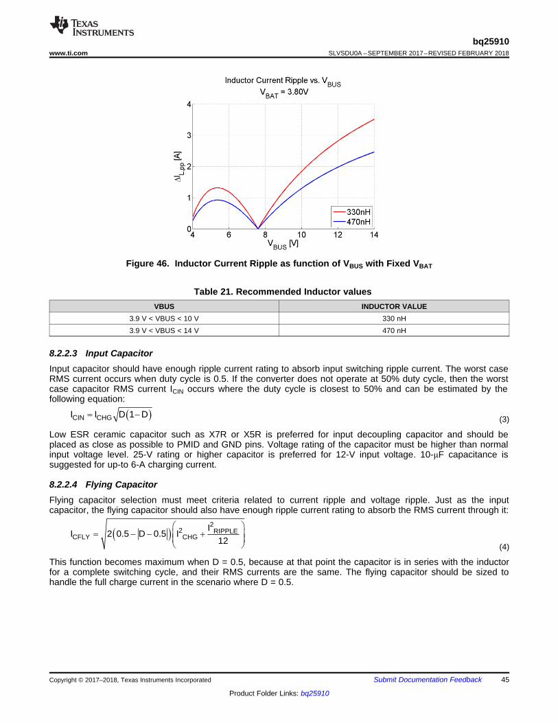
� �2
2 RIPPLECFLY CHG
II 2 0.5 D 0.5 I
12
§ · � � �¨ ¸¨ ¸
© ¹
� �CIN CHGI I D 1 D �
45
bq25910www.ti.com SLVSDU0A –SEPTEMBER 2017–REVISED FEBRUARY 2018
Product Folder Links: bq25910
Submit Documentation FeedbackCopyright © 2017–2018, Texas Instruments Incorporated
Figure 46. Inductor Current Ripple as function of VBUS with Fixed VBAT
Table 21. Recommended Inductor valuesVBUS INDUCTOR VALUE
3.9 V < VBUS < 10 V 330 nH3.9 V < VBUS < 14 V 470 nH
8.2.2.3 Input CapacitorInput capacitor should have enough ripple current rating to absorb input switching ripple current. The worst caseRMS current occurs when duty cycle is 0.5. If the converter does not operate at 50% duty cycle, then the worstcase capacitor RMS current ICIN occurs where the duty cycle is closest to 50% and can be estimated by thefollowing equation:
(3)
Low ESR ceramic capacitor such as X7R or X5R is preferred for input decoupling capacitor and should beplaced as close as possible to PMID and GND pins. Voltage rating of the capacitor must be higher than normalinput voltage level. 25-V rating or higher capacitor is preferred for 12-V input voltage. 10-μF capacitance issuggested for up-to 6-A charging current.
8.2.2.4 Flying CapacitorFlying capacitor selection must meet criteria related to current ripple and voltage ripple. Just as the inputcapacitor, the flying capacitor should also have enough ripple current rating to absorb the RMS current through it:
(4)
This function becomes maximum when D = 0.5, because at that point the capacitor is in series with the inductorfor a complete switching cycle, and their RMS currents are the same. The flying capacitor should be sized tohandle the full charge current in the scenario where D = 0.5.

� �CHGCFLY
FLY SW
I 0.5 D 0.5V
C f
� �'
46
bq25910SLVSDU0A –SEPTEMBER 2017–REVISED FEBRUARY 2018 www.ti.com
Product Folder Links: bq25910
Submit Documentation Feedback Copyright © 2017–2018, Texas Instruments Incorporated
Figure 47. Flying Capacitor RMS Current vs. VBUS with Fixed VBAT and ICHG
Additionally, the flying capacitor voltage ripple should be kept under 10% of VBUS/2 to ensure loop stability. Thisquantity is given by the following equation:
(5)
It is recommended to use at least two 16-V, 10-μF, low ESR ceramic capacitors in parallel to achieve both RMScurrent rating and maintain voltage ripple <10% in the flying capacitor for up-to 6-A charge current application.The following curve shows what the ripple voltage of CFLY might look like for such a configuration by taking intoaccount voltage derating of the capacitor and plugging the effective capacitance value into equation above atdifferent charge currents and VBUS voltages.
Figure 48. Flying Capacitor Ripple Voltage vs. VBUS with Fixed VBAT
Table 22. Recommended CFLY ValuesCHARGE CURRENT CFLY CONFIGURATION
ICHG < 3.5 A 1 x 0603 (10 μF, X5R, 16 V)ICHG > 3.5 A 2 x 0603 (10 μF, X5R, 16 V)

RIPPLESYS
O SW
IV
16C f'
RIPPLECOUT RIPPLE
II 0.29 I
2 3 | u
47
bq25910www.ti.com SLVSDU0A –SEPTEMBER 2017–REVISED FEBRUARY 2018
Product Folder Links: bq25910
Submit Documentation FeedbackCopyright © 2017–2018, Texas Instruments Incorporated
8.2.2.5 Output CapacitorOutput capacitor also should have enough ripple current rating to absorb output switching ripple current. Theoutput capacitor RMS current ICOUT is given:
(6)
The output capacitor voltage ripple can be calculated as follows:
(7)
At certain input/output voltage and switching frequency, the voltage ripple can be reduced by increasing theoutput filter LC. The preferred ceramic capacitor is 20 μF, 6.3 V or higher rating, X7R or X5R.
8.2.3 Application CurvesCBUS = 1 µF, CPMID = 10 µF, CBAT = 20 µF, CFLY = 20 µF, L = DFE252012F-R47 (470 nH) (unless otherwise noted)
VBUS = 5 V, VBAT = 3.8 V
Figure 49. Adapter Power Up with Charge Enabled
VBUS = 12 V, VBAT = 3.8 V
Figure 50. HV Adapter Power Up with Charge Enabled
VBUS = 5 V, VBAT = 3.5 V, ICHG = 3 A
Figure 51. Charge Disable
VBUS = 12 V, VBAT = 3.5 V, ICHG = 4 A
Figure 52. HV Adapter Charge Disable

48
bq25910SLVSDU0A –SEPTEMBER 2017–REVISED FEBRUARY 2018 www.ti.com
Product Folder Links: bq25910
Submit Documentation Feedback Copyright © 2017–2018, Texas Instruments Incorporated
CBUS = 1 µF, CPMID = 10 µF, CBAT = 20 µF, CFLY = 20 µF, L = DFE252012F-R47 (470 nH) (unless otherwise noted)
VBUS = 5 V -> 12 V -> 5 V, VBAT = 4 V, ICHG = 1 ACH 1 = VBUS, CH2 = SW, CH3 = CFLY differential, CH4 =VBAT
Figure 53. Line Transient Response in CC Mode
VBUS = 12 V, VBAT = 4.35 V, ICHG = 4 A, IBAT = 1 A -> 4 A ->1 ACH 1 = VBUS, CH2 = ILOAD, CH3 = CFLY differential, CH4 =VBAT
Figure 54. Load Transient Response in CV Mode
VBAT = 4.1 V, VINDPM = 4.3 V
Figure 55. VINDPM Response
VBUS = 5 V, VBAT = 3.8 V, ICHG = 2 A, (D > 50%)
Figure 56. PWM Switching Waveform
VBUS = 8 V, VBAT = 3.8 V, ICHG = 2 A, (D approx. 50%)
Figure 57. PWM Switching Waveform
VBUS = 12 V, VBAT = 3.8 V, ICHG = 2 A (D < 50%)
Figure 58. PWM Switching Waveform

49
bq25910www.ti.com SLVSDU0A –SEPTEMBER 2017–REVISED FEBRUARY 2018
Product Folder Links: bq25910
Submit Documentation FeedbackCopyright © 2017–2018, Texas Instruments Incorporated
CBUS = 1 µF, CPMID = 10 µF, CBAT = 20 µF, CFLY = 20 µF, L = DFE252012F-R47 (470 nH) (unless otherwise noted)
VBUS = 5 V, VBAT = 3.8 V
Figure 59. Adapter Removal
VBUS = 12 V, VBAT = 3.8 V
Figure 60. Adapter Removal

50
bq25910SLVSDU0A –SEPTEMBER 2017–REVISED FEBRUARY 2018 www.ti.com
Product Folder Links: bq25910
Submit Documentation Feedback Copyright © 2017–2018, Texas Instruments Incorporated
9 Power Supply RecommendationsIn order to charge single-cell Li-Ion battery, the device requires a power supply between 3.9 V and 14 V with atleast 500-mA current rating connected to VBUS. Additionally, a single-cell Li-Ion battery with voltage > VBAT_LOWVshould be connected between at the output of the switched inductor, between BATP and BATN terminals.

51
bq25910www.ti.com SLVSDU0A –SEPTEMBER 2017–REVISED FEBRUARY 2018
Product Folder Links: bq25910
Submit Documentation FeedbackCopyright © 2017–2018, Texas Instruments Incorporated
10 Layout
10.1 Layout GuidelinesThe switching node rise and fall times should be minimized for minimum switching loss. Proper layout of thecomponents to minimize high frequency current path loops is important to prevent electrical and magnetic fieldradiation and high-frequency resonant problems. Here is a PCB layout priority list for proper layout. Layout PCBaccording to this specific order is essential.1. Utilize at least four-layer board for optimal layout, and assign one layer as solid ground plane near the IC to
minimize high-frequency current path2. Place flying capacitor as close to CLFY+ and CLFY– bumps as possible. Minimize the copper area of this
trace to lower electrical and magnetic field radiation but make the trace wide enough to carry the chargingcurrent. Do not use multiple layers in parallel for this connection.
3. Place input capacitor as close as possible to PMID bumps and PGND bumps and use solid GND planeunderneath the IC. Use plenty of vias close to PMID capacitor GND terminal and IC PGND bumps to ensurelow parasitic connection to GND plane.
4. Place inductor input terminal as close to SW bumps as possible. Minimize the copper area of this trace tolower electrical and magnetic field radiation but make the trace wide enough to carry the charging current.
5. Put output capacitor near to the inductor and the device. Ground connections need to be tied to the deviceground with a short copper trace connection or GND plane.
6. Decoupling capacitors should be placed next to the device and make trace connection as short as possible.7. Ensure that there are sufficient thermal vias directly under bumps of the power FETs, connecting to copper
on other layers.8. The via size and number should be enough for a given current path.9. Route BATP and BATN away from switching nodes such as SW and CFLY+, CFLY–.
Refer to the EVM design and Figure 61 for the recommended component placement with trace and vialocations.

VBUS PMID C+ SW C- GND
VBUS PMID C+ SW C- GND
VBUS PMID C+ SW C- GND
CDRV+ PMID C+ SW C- GND
SDA INT SW C- GND
BATN BATPIND_SNS
VBUSPMID C+ C-
GND
GND
CDRV-
CDRV+
BATP
CAUX
SCL
GND
0603
0603
0603
0603
0603
0603
1008SW
CDRV-
SCL
0201
GND
GND
0402
BATN/INT
CAUX REGN
0402
BAT
REGN
SDA
52
bq25910SLVSDU0A –SEPTEMBER 2017–REVISED FEBRUARY 2018 www.ti.com
Product Folder Links: bq25910
Submit Documentation Feedback Copyright © 2017–2018, Texas Instruments Incorporated
10.2 Layout Example
Figure 61. bq25910 PCB Layout Example

53
bq25910www.ti.com SLVSDU0A –SEPTEMBER 2017–REVISED FEBRUARY 2018
Product Folder Links: bq25910
Submit Documentation FeedbackCopyright © 2017–2018, Texas Instruments Incorporated
11 Device and Documentation Support
11.1 Device Support
11.1.1 Third-Party Products Disclaimer
11.1.1.1 Third-Party Products DisclaimerTI'S PUBLICATION OF INFORMATION REGARDING THIRD-PARTY PRODUCTS OR SERVICES DOES NOTCONSTITUTE AN ENDORSEMENT REGARDING THE SUITABILITY OF SUCH PRODUCTS OR SERVICESOR A WARRANTY, REPRESENTATION OR ENDORSEMENT OF SUCH PRODUCTS OR SERVICES, EITHERALONE OR IN COMBINATION WITH ANY TI PRODUCT OR SERVICE.
11.2 Receiving Notification of Documentation UpdatesTo receive notification of documentation updates, navigate to the device product folder on ti.com. In the upperright corner, click on Alert me to register and receive a weekly digest of any product information that haschanged. For change details, review the revision history included in any revised document.
11.3 Community ResourcesThe following links connect to TI community resources. Linked contents are provided "AS IS" by the respectivecontributors. They do not constitute TI specifications and do not necessarily reflect TI's views; see TI's Terms ofUse.
TI E2E™ Online Community TI's Engineer-to-Engineer (E2E) Community. Created to foster collaborationamong engineers. At e2e.ti.com, you can ask questions, share knowledge, explore ideas and helpsolve problems with fellow engineers.
Design Support TI's Design Support Quickly find helpful E2E forums along with design support tools andcontact information for technical support.
11.4 TrademarksE2E is a trademark of Texas Instruments.All other trademarks are the property of their respective owners.
11.5 Electrostatic Discharge CautionThis integrated circuit can be damaged by ESD. Texas Instruments recommends that all integrated circuits be handled withappropriate precautions. Failure to observe proper handling and installation procedures can cause damage.
ESD damage can range from subtle performance degradation to complete device failure. Precision integrated circuits may be moresusceptible to damage because very small parametric changes could cause the device not to meet its published specifications.
11.6 GlossarySLYZ022 — TI Glossary.
This glossary lists and explains terms, acronyms, and definitions.
12 Mechanical, Packaging, and Orderable InformationThe following pages include mechanical, packaging, and orderable information. This information is the mostcurrent data available for the designated devices. This data is subject to change without notice and revision ofthis document. For browser-based versions of this data sheet, refer to the left-hand navigation.

PACKAGE OPTION ADDENDUM
www.ti.com 9-Mar-2018
Addendum-Page 1
PACKAGING INFORMATION
Orderable Device Status(1)
Package Type PackageDrawing
Pins PackageQty
Eco Plan(2)
Lead/Ball Finish(6)
MSL Peak Temp(3)
Op Temp (°C) Device Marking(4/5)
Samples
BQ25910YFFR ACTIVE DSBGA YFF 36 3000 Green (RoHS& no Sb/Br)
SNAGCU Level-1-260C-UNLIM -40 to 85 BQ25910
BQ25910YFFT ACTIVE DSBGA YFF 36 250 Green (RoHS& no Sb/Br)
SNAGCU Level-1-260C-UNLIM -40 to 85 BQ25910
PQ25910YFFT ACTIVE DSBGA YFF 36 250 TBD Call TI Call TI -40 to 85
(1) The marketing status values are defined as follows:ACTIVE: Product device recommended for new designs.LIFEBUY: TI has announced that the device will be discontinued, and a lifetime-buy period is in effect.NRND: Not recommended for new designs. Device is in production to support existing customers, but TI does not recommend using this part in a new design.PREVIEW: Device has been announced but is not in production. Samples may or may not be available.OBSOLETE: TI has discontinued the production of the device.
(2) RoHS: TI defines "RoHS" to mean semiconductor products that are compliant with the current EU RoHS requirements for all 10 RoHS substances, including the requirement that RoHS substancedo not exceed 0.1% by weight in homogeneous materials. Where designed to be soldered at high temperatures, "RoHS" products are suitable for use in specified lead-free processes. TI mayreference these types of products as "Pb-Free".RoHS Exempt: TI defines "RoHS Exempt" to mean products that contain lead but are compliant with EU RoHS pursuant to a specific EU RoHS exemption.Green: TI defines "Green" to mean the content of Chlorine (Cl) and Bromine (Br) based flame retardants meet JS709B low halogen requirements of <=1000ppm threshold. Antimony trioxide basedflame retardants must also meet the <=1000ppm threshold requirement.
(3) MSL, Peak Temp. - The Moisture Sensitivity Level rating according to the JEDEC industry standard classifications, and peak solder temperature.
(4) There may be additional marking, which relates to the logo, the lot trace code information, or the environmental category on the device.
(5) Multiple Device Markings will be inside parentheses. Only one Device Marking contained in parentheses and separated by a "~" will appear on a device. If a line is indented then it is a continuationof the previous line and the two combined represent the entire Device Marking for that device.
(6) Lead/Ball Finish - Orderable Devices may have multiple material finish options. Finish options are separated by a vertical ruled line. Lead/Ball Finish values may wrap to two lines if the finishvalue exceeds the maximum column width.
Important Information and Disclaimer:The information provided on this page represents TI's knowledge and belief as of the date that it is provided. TI bases its knowledge and belief on informationprovided by third parties, and makes no representation or warranty as to the accuracy of such information. Efforts are underway to better integrate information from third parties. TI has taken andcontinues to take reasonable steps to provide representative and accurate information but may not have conducted destructive testing or chemical analysis on incoming materials and chemicals.TI and TI suppliers consider certain information to be proprietary, and thus CAS numbers and other limited information may not be available for release.

PACKAGE OPTION ADDENDUM
www.ti.com 9-Mar-2018
Addendum-Page 2
In no event shall TI's liability arising out of such information exceed the total purchase price of the TI part(s) at issue in this document sold by TI to Customer on an annual basis.

TAPE AND REEL INFORMATION
*All dimensions are nominal
Device PackageType
PackageDrawing
Pins SPQ ReelDiameter
(mm)
ReelWidth
W1 (mm)
A0(mm)
B0(mm)
K0(mm)
P1(mm)
W(mm)
Pin1Quadrant
BQ25910YFFR DSBGA YFF 36 3000 180.0 8.4 2.54 2.54 0.76 4.0 8.0 Q1
BQ25910YFFT DSBGA YFF 36 250 180.0 8.4 2.54 2.54 0.76 4.0 8.0 Q1
PACKAGE MATERIALS INFORMATION
www.ti.com 30-Apr-2018
Pack Materials-Page 1

*All dimensions are nominal
Device Package Type Package Drawing Pins SPQ Length (mm) Width (mm) Height (mm)
BQ25910YFFR DSBGA YFF 36 3000 182.0 182.0 20.0
BQ25910YFFT DSBGA YFF 36 250 182.0 182.0 20.0
PACKAGE MATERIALS INFORMATION
www.ti.com 30-Apr-2018
Pack Materials-Page 2

www.ti.com
PACKAGE OUTLINE
C0.625 MAX
0.300.12
2TYP
2 TYP
0.4 TYP
0.4 TYP
36X 0.30.2
B E A
D
4222008/A 03/2015
DSBGA - 0.625 mm max heightYFF0036DIE SIZE BALL GRID ARRAY
NOTES: 1. All linear dimensions are in millimeters. Any dimensions in parenthesis are for reference only. Dimensioning and tolerancing per ASME Y14.5M. 2. This drawing is subject to change without notice.
BUMP A1CORNER
SEATING PLANE
BALL TYP 0.05 C
A
B
C
D
1 2 3 0.015 C A B
E
54
F
SYMM
SYMM
6
SCALE 4.500
D: Max =
E: Max =
2.472 mm, Min =
2.444 mm, Min =
2.412 mm
2.384 mm

www.ti.com
EXAMPLE BOARD LAYOUT
36X ( )0.23(0.4) TYP
(0.4) TYP
( )METAL
0.23 0.05 MAX
SOLDER MASKOPENING
METAL UNDERSOLDER MASK
( )SOLDER MASKOPENING
0.230.05 MIN
4222008/A 03/2015
DSBGA - 0.625 mm max heightYFF0036DIE SIZE BALL GRID ARRAY
NOTES: (continued) 3. Final dimensions may vary due to manufacturing tolerance considerations and also routing constraints. For more information, see Texas Instruments literature number SNVA009 (www.ti.com/lit/snva009).
SOLDER MASK DETAILSNOT TO SCALE
SYMM
SYMM
LAND PATTERN EXAMPLESCALE:25X
A
B
C
D
1 2 3 4 5
E
F
6
NON-SOLDER MASKDEFINED
(PREFERRED)
SOLDER MASKDEFINED

www.ti.com
EXAMPLE STENCIL DESIGN
(0.4)TYP
(0.4) TYP
36X ( 0.25)(R ) TYP0.05
METALTYP
4222008/A 03/2015
DSBGA - 0.625 mm max heightYFF0036DIE SIZE BALL GRID ARRAY
NOTES: (continued) 4. Laser cutting apertures with trapezoidal walls and rounded corners may offer better paste release.
SYMM
SYMM
SOLDER PASTE EXAMPLEBASED ON 0.1 mm THICK STENCIL
SCALE:30X
A
B
C
D
1 2 3
E
4 5
F
6

IMPORTANT NOTICE
Texas Instruments Incorporated (TI) reserves the right to make corrections, enhancements, improvements and other changes to itssemiconductor products and services per JESD46, latest issue, and to discontinue any product or service per JESD48, latest issue. Buyersshould obtain the latest relevant information before placing orders and should verify that such information is current and complete.TI’s published terms of sale for semiconductor products (http://www.ti.com/sc/docs/stdterms.htm) apply to the sale of packaged integratedcircuit products that TI has qualified and released to market. Additional terms may apply to the use or sale of other types of TI products andservices.Reproduction of significant portions of TI information in TI data sheets is permissible only if reproduction is without alteration and isaccompanied by all associated warranties, conditions, limitations, and notices. TI is not responsible or liable for such reproduceddocumentation. Information of third parties may be subject to additional restrictions. Resale of TI products or services with statementsdifferent from or beyond the parameters stated by TI for that product or service voids all express and any implied warranties for theassociated TI product or service and is an unfair and deceptive business practice. TI is not responsible or liable for any such statements.Buyers and others who are developing systems that incorporate TI products (collectively, “Designers”) understand and agree that Designersremain responsible for using their independent analysis, evaluation and judgment in designing their applications and that Designers havefull and exclusive responsibility to assure the safety of Designers' applications and compliance of their applications (and of all TI productsused in or for Designers’ applications) with all applicable regulations, laws and other applicable requirements. Designer represents that, withrespect to their applications, Designer has all the necessary expertise to create and implement safeguards that (1) anticipate dangerousconsequences of failures, (2) monitor failures and their consequences, and (3) lessen the likelihood of failures that might cause harm andtake appropriate actions. Designer agrees that prior to using or distributing any applications that include TI products, Designer willthoroughly test such applications and the functionality of such TI products as used in such applications.TI’s provision of technical, application or other design advice, quality characterization, reliability data or other services or information,including, but not limited to, reference designs and materials relating to evaluation modules, (collectively, “TI Resources”) are intended toassist designers who are developing applications that incorporate TI products; by downloading, accessing or using TI Resources in anyway, Designer (individually or, if Designer is acting on behalf of a company, Designer’s company) agrees to use any particular TI Resourcesolely for this purpose and subject to the terms of this Notice.TI’s provision of TI Resources does not expand or otherwise alter TI’s applicable published warranties or warranty disclaimers for TIproducts, and no additional obligations or liabilities arise from TI providing such TI Resources. TI reserves the right to make corrections,enhancements, improvements and other changes to its TI Resources. TI has not conducted any testing other than that specificallydescribed in the published documentation for a particular TI Resource.Designer is authorized to use, copy and modify any individual TI Resource only in connection with the development of applications thatinclude the TI product(s) identified in such TI Resource. NO OTHER LICENSE, EXPRESS OR IMPLIED, BY ESTOPPEL OR OTHERWISETO ANY OTHER TI INTELLECTUAL PROPERTY RIGHT, AND NO LICENSE TO ANY TECHNOLOGY OR INTELLECTUAL PROPERTYRIGHT OF TI OR ANY THIRD PARTY IS GRANTED HEREIN, including but not limited to any patent right, copyright, mask work right, orother intellectual property right relating to any combination, machine, or process in which TI products or services are used. Informationregarding or referencing third-party products or services does not constitute a license to use such products or services, or a warranty orendorsement thereof. Use of TI Resources may require a license from a third party under the patents or other intellectual property of thethird party, or a license from TI under the patents or other intellectual property of TI.TI RESOURCES ARE PROVIDED “AS IS” AND WITH ALL FAULTS. TI DISCLAIMS ALL OTHER WARRANTIES ORREPRESENTATIONS, EXPRESS OR IMPLIED, REGARDING RESOURCES OR USE THEREOF, INCLUDING BUT NOT LIMITED TOACCURACY OR COMPLETENESS, TITLE, ANY EPIDEMIC FAILURE WARRANTY AND ANY IMPLIED WARRANTIES OFMERCHANTABILITY, FITNESS FOR A PARTICULAR PURPOSE, AND NON-INFRINGEMENT OF ANY THIRD PARTY INTELLECTUALPROPERTY RIGHTS. TI SHALL NOT BE LIABLE FOR AND SHALL NOT DEFEND OR INDEMNIFY DESIGNER AGAINST ANY CLAIM,INCLUDING BUT NOT LIMITED TO ANY INFRINGEMENT CLAIM THAT RELATES TO OR IS BASED ON ANY COMBINATION OFPRODUCTS EVEN IF DESCRIBED IN TI RESOURCES OR OTHERWISE. IN NO EVENT SHALL TI BE LIABLE FOR ANY ACTUAL,DIRECT, SPECIAL, COLLATERAL, INDIRECT, PUNITIVE, INCIDENTAL, CONSEQUENTIAL OR EXEMPLARY DAMAGES INCONNECTION WITH OR ARISING OUT OF TI RESOURCES OR USE THEREOF, AND REGARDLESS OF WHETHER TI HAS BEENADVISED OF THE POSSIBILITY OF SUCH DAMAGES.Unless TI has explicitly designated an individual product as meeting the requirements of a particular industry standard (e.g., ISO/TS 16949and ISO 26262), TI is not responsible for any failure to meet such industry standard requirements.Where TI specifically promotes products as facilitating functional safety or as compliant with industry functional safety standards, suchproducts are intended to help enable customers to design and create their own applications that meet applicable functional safety standardsand requirements. Using products in an application does not by itself establish any safety features in the application. Designers mustensure compliance with safety-related requirements and standards applicable to their applications. Designer may not use any TI products inlife-critical medical equipment unless authorized officers of the parties have executed a special contract specifically governing such use.Life-critical medical equipment is medical equipment where failure of such equipment would cause serious bodily injury or death (e.g., lifesupport, pacemakers, defibrillators, heart pumps, neurostimulators, and implantables). Such equipment includes, without limitation, allmedical devices identified by the U.S. Food and Drug Administration as Class III devices and equivalent classifications outside the U.S.TI may expressly designate certain products as completing a particular qualification (e.g., Q100, Military Grade, or Enhanced Product).Designers agree that it has the necessary expertise to select the product with the appropriate qualification designation for their applicationsand that proper product selection is at Designers’ own risk. Designers are solely responsible for compliance with all legal and regulatoryrequirements in connection with such selection.Designer will fully indemnify TI and its representatives against any damages, costs, losses, and/or liabilities arising out of Designer’s non-compliance with the terms and provisions of this Notice.
Mailing Address: Texas Instruments, Post Office Box 655303, Dallas, Texas 75265Copyright © 2018, Texas Instruments Incorporated