broadband mm-wave transceivers for sensing and communication
TRANSCRIPT

Broadband mm-Wave Transceivers for Sensing andCommunication
Andrew Townley
Electrical Engineering and Computer SciencesUniversity of California at Berkeley
Technical Report No. UCB/EECS-2020-25http://www2.eecs.berkeley.edu/Pubs/TechRpts/2020/EECS-2020-25.html
May 1, 2020

Copyright © 2020, by the author(s).All rights reserved.
Permission to make digital or hard copies of all or part of this work forpersonal or classroom use is granted without fee provided that copies arenot made or distributed for profit or commercial advantage and that copiesbear this notice and the full citation on the first page. To copy otherwise, torepublish, to post on servers or to redistribute to lists, requires prior specificpermission.

Broadband mm-Wave Transceivers forSensing and Communication
by
Andrew Townley
A dissertation submitted in partial satisfaction of the
requirements for the degree of
Doctor of Philosophy
in
Engineering — Electrical Engineering and Computer Sciences
in the
Graduate Division
of the
University of California, Berkeley
Committee in charge:
Professor Ali M. Niknejad, ChairProfessor Elad Alon
Professor Martin White
Spring 2018

The dissertation of Andrew Townley, titled Broadband mm-Wave Transceivers forSensing and Communication, is approved:
Chair Date
Date
Date
University of California, Berkeley

Broadband mm-Wave Transceivers forSensing and Communication
Copyright 2018by
Andrew Townley

1
Abstract
Broadband mm-Wave Transceivers forSensing and Communication
by
Andrew Townley
Doctor of Philosophy in Engineering — Electrical Engineering and Computer Sciences
University of California, Berkeley
Professor Ali M. Niknejad, Chair
Scaling in silicon semiconductor process technology, although driven by digital applica-tions, has also enabled the operation of analog integrated circuits (ICs) at higher and higherfrequencies. Over the past 15-20 years, ICs operating at millimeter-wave (mm-Wave), thefrequency range between 30 GHz and 300 GHz, have been demonstrated with increasingperformance and complexity.
One important application for mm-Wave ICs has been in automotive radar, where theyhave been used to make accurate measurements of distance and velocity with minimal pro-cessing required. There also has been significant interest in adapting this technology fornon-vehicular applications, such as gesture recognition, room occupancy detection, or heart-rate monitoring, where performance and energy efficiency are both important. The first partof this thesis describes a custom IC for gesture recognition radar demonstrating state-of-the-art energy efficiency. The IC consists of four transmitters and four receivers with sharedfrequency generation circuitry, and is packaged onto a 1.2x1.2cm antenna module containingeight antennas.
The other key application for mm-Wave technology has been for wireless communication.Products are finally coming to the market now that offer nearly 5 Gigabits per second ofwireless data throughput for indoor wireless LAN applications, and mm-Wave technology willlikely play a role in the next generation of wireless cellular standards as well. To demonstratethe possibility for yet-higher data rates to be achieved, a broad-bandwidth custom integratedcircuit transceiver has been designed targeting a factor of 10 improvement in wireless datathroughput beyond commercially available technology. The second half of this thesis willdiscuss the details of a transceiver and antenna design for broad-bandwidth and high datarate operation.

i
To my parents,
without whose love and encouragement I never could have made it this far.

ii
Contents
Contents ii
List of Figures iv
List of Tables ix
1 Introduction 11.1 Motivation . . . . . . . . . . . . . . . . . . . . . . . . . . . . . . . . . . . . . 2
2 Millimeter-Wave Background 42.1 Technology: Bipolar vs MOSFET . . . . . . . . . . . . . . . . . . . . . . . . 42.2 LO Generation and Distribution . . . . . . . . . . . . . . . . . . . . . . . . . 52.3 Modulation Techniques . . . . . . . . . . . . . . . . . . . . . . . . . . . . . . 5
2.3.1 Modulation Techniques for Radar . . . . . . . . . . . . . . . . . . . . 52.3.2 Modulation Techniques for Digital Communication . . . . . . . . . . 7
2.4 Phased Array Techniques . . . . . . . . . . . . . . . . . . . . . . . . . . . . . 10
3 FMCW Radar Phased-Array Transceiver Design 113.1 Proposed System Architecture . . . . . . . . . . . . . . . . . . . . . . . . . . 113.2 Transmitter . . . . . . . . . . . . . . . . . . . . . . . . . . . . . . . . . . . . 133.3 Phase Shifter . . . . . . . . . . . . . . . . . . . . . . . . . . . . . . . . . . . 163.4 LO Distribution . . . . . . . . . . . . . . . . . . . . . . . . . . . . . . . . . . 183.5 Receiver . . . . . . . . . . . . . . . . . . . . . . . . . . . . . . . . . . . . . . 223.6 Packaging . . . . . . . . . . . . . . . . . . . . . . . . . . . . . . . . . . . . . 25
4 Radar IC Measurements 284.1 Probe Station Measurements . . . . . . . . . . . . . . . . . . . . . . . . . . . 29
4.1.1 LO . . . . . . . . . . . . . . . . . . . . . . . . . . . . . . . . . . . . . 294.1.2 Transmitter . . . . . . . . . . . . . . . . . . . . . . . . . . . . . . . . 294.1.3 Receiver . . . . . . . . . . . . . . . . . . . . . . . . . . . . . . . . . . 30
4.2 Packaged Measurements . . . . . . . . . . . . . . . . . . . . . . . . . . . . . 314.2.1 Array Characterization . . . . . . . . . . . . . . . . . . . . . . . . . . 314.2.2 Radar Measurements and Characterization . . . . . . . . . . . . . . . 35

iii
4.3 Conclusion . . . . . . . . . . . . . . . . . . . . . . . . . . . . . . . . . . . . . 37
5 Wideband mm-Wave Transceiver Design 405.1 Motivation and System Architecture . . . . . . . . . . . . . . . . . . . . . . 40
5.1.1 System Architecture . . . . . . . . . . . . . . . . . . . . . . . . . . . 415.1.2 Packaging Approach . . . . . . . . . . . . . . . . . . . . . . . . . . . 42
5.2 Building Blocks . . . . . . . . . . . . . . . . . . . . . . . . . . . . . . . . . . 445.2.1 Modular Common-Source Neutralized Amplifier Layout . . . . . . . . 445.2.2 Coupled Resonators using Low-K Transformers . . . . . . . . . . . . 455.2.3 Low-K Transformers with Lossy Inductors . . . . . . . . . . . . . . . 49
5.3 Transmitter . . . . . . . . . . . . . . . . . . . . . . . . . . . . . . . . . . . . 515.3.1 Modulator Design . . . . . . . . . . . . . . . . . . . . . . . . . . . . . 515.3.2 Power Amplifier Design . . . . . . . . . . . . . . . . . . . . . . . . . . 685.3.3 TX Chain Simulated Results . . . . . . . . . . . . . . . . . . . . . . . 71
5.4 Receiver . . . . . . . . . . . . . . . . . . . . . . . . . . . . . . . . . . . . . . 745.4.1 Baseband Amplification . . . . . . . . . . . . . . . . . . . . . . . . . 745.4.2 Active Mixer with TIA load . . . . . . . . . . . . . . . . . . . . . . . 755.4.3 LNA . . . . . . . . . . . . . . . . . . . . . . . . . . . . . . . . . . . . 815.4.4 RX Chain Simulated Performance . . . . . . . . . . . . . . . . . . . . 83
5.5 PCB and Antenna Design . . . . . . . . . . . . . . . . . . . . . . . . . . . . 845.5.1 Folded Dipole Antenna . . . . . . . . . . . . . . . . . . . . . . . . . . 855.5.2 Surface Waves . . . . . . . . . . . . . . . . . . . . . . . . . . . . . . . 885.5.3 Methods for Dealing with Surface Waves . . . . . . . . . . . . . . . . 895.5.4 Planar Balun on PCB . . . . . . . . . . . . . . . . . . . . . . . . . . 94
5.6 Fabricated Transceiver and Antenna PCB . . . . . . . . . . . . . . . . . . . 985.7 Performance Comparison . . . . . . . . . . . . . . . . . . . . . . . . . . . . . 101
6 Conclusion 1026.1 Summary of Thesis . . . . . . . . . . . . . . . . . . . . . . . . . . . . . . . . 1026.2 Future Work . . . . . . . . . . . . . . . . . . . . . . . . . . . . . . . . . . . . 103
6.2.1 Carrier Recovery . . . . . . . . . . . . . . . . . . . . . . . . . . . . . 1036.2.2 Equalization . . . . . . . . . . . . . . . . . . . . . . . . . . . . . . . . 104
Bibliography 105
iv
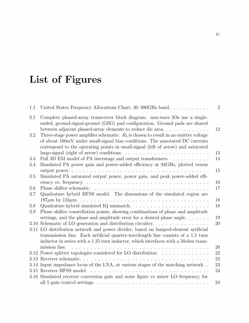
List of Figures
1.1 United States Frequency Allocations Chart, 30–300GHz band. . . . . . . . . . . 2
3.1 Complete phased-array transceiver block diagram. mm-wave IOs use a single-ended, ground-signal-ground (GSG) pad configuration. Ground pads are sharedbetween adjacent phased-array elements to reduce die area. . . . . . . . . . . . . 12
3.2 Three-stage power amplifier schematic. R5 is chosen to result in an emitter voltageof about 100mV under small-signal bias conditions. The annotated DC currentscorrespond to the operating points in small-signal (left of arrow) and saturatedlarge-signal (right of arrow) conditions. . . . . . . . . . . . . . . . . . . . . . . . 13
3.3 Full 3D EM model of PA interstage and output transformers. . . . . . . . . . . 143.4 Simulated PA power gain and power-added efficiency at 94GHz, plotted versus
output power. . . . . . . . . . . . . . . . . . . . . . . . . . . . . . . . . . . . . . 153.5 Simulated PA saturated output power, power gain, and peak power-added effi-
ciency vs. frequency. . . . . . . . . . . . . . . . . . . . . . . . . . . . . . . . . . 163.6 Phase shifter schematic. . . . . . . . . . . . . . . . . . . . . . . . . . . . . . . . 173.7 Quadrature hybrid HFSS model. The dimensions of the simulated region are
197µm by 124µm. . . . . . . . . . . . . . . . . . . . . . . . . . . . . . . . . . . . 183.8 Quadrature hybrid simulated IQ mismatch. . . . . . . . . . . . . . . . . . . . . 183.9 Phase shifter constellation points, showing combinations of phase and amplitude
settings, and the phase and amplitude error for a desired phase angle. . . . . . . 193.10 Schematic of LO generation and distribution circuitry. . . . . . . . . . . . . . . 203.11 LO distribution network and power divider, based on lumped-element artificial
transmission line. Each artificial quarter-wavelength line consists of a 1.5 turninductor in series with a 1.25 turn inductor, which interfaces with a 50ohm trans-mission line. . . . . . . . . . . . . . . . . . . . . . . . . . . . . . . . . . . . . . 20
3.12 Power splitter topologies considered for LO distribution. . . . . . . . . . . . . . 223.13 Receiver schematic. . . . . . . . . . . . . . . . . . . . . . . . . . . . . . . . . . . 223.14 Input impedance locus of the LNA, at various stages of the matching network. . 233.15 Receiver HFSS model. . . . . . . . . . . . . . . . . . . . . . . . . . . . . . . . . 243.16 Simulated receiver conversion gain and noise figure vs mixer LO frequency, for
all 5 gain control settings. . . . . . . . . . . . . . . . . . . . . . . . . . . . . . . 24

v
3.17 (a) Percentage contributions of different blocks to total output noise. The con-tributions are separated by sideband. (b) Noise circles . . . . . . . . . . . . . . 25
3.18 HFSS simulations of antenna module. . . . . . . . . . . . . . . . . . . . . . . . . 253.19 Levels of integration of radar IC. Bare die (a) is flip-chip chip packaged onto BGA
antenna module (b), which is integrated onto a test PCB (c). The test PCB is10.2cm x 10.2cm, sized to accomodate connectors to a separate FPGA board. Ifa microcontroller were used instead of an FPGA, the board area could be reducedto a much smaller size. . . . . . . . . . . . . . . . . . . . . . . . . . . . . . . . . 26
3.20 Photograph of 1.2cm×1.2cm BGA antenna module with die attached, chip (left)and antenna (right) sides. . . . . . . . . . . . . . . . . . . . . . . . . . . . . . . 27
4.1 Die photograph of fabricated chip. . . . . . . . . . . . . . . . . . . . . . . . . . 284.2 VCO tuning curve, and measured phase noise of PLL at 94GHz. . . . . . . . . . 294.3 Measured transmitter output power vs frequency. . . . . . . . . . . . . . . . . . 304.4 The measured LNA input impedance (a) and PA output impedance (b) showed
good agreement with simulation. . . . . . . . . . . . . . . . . . . . . . . . . . . 304.5 Measured receiver single-sideband noise figure (probe station) vs frequency. . . . 314.6 EIRP at broadside vs frequency, for 1, 2, and 4 PAs enabled. All possible com-
binations of the 1 and 2 PA cases are plotted. . . . . . . . . . . . . . . . . . . . 324.7 Beam steering of transmitter at 94GHz, characterized manually at BWRC. . . . 334.8 RX array conversion gain vs frequency, for 1, 2, and 4 LNAs enabled. All possible
combinations of the 1 and 2 LNA cases are plotted. . . . . . . . . . . . . . . . . 334.9 Measured phase shifter constellation points, with circle showing amplitude level
with least average amplitude error. . . . . . . . . . . . . . . . . . . . . . . . . . 344.10 The measurement setup at University of Nice-Sophia Antipolis. The test PCB is
placed with the radiating side downward, and the arm with the receive antennais swept across phi and theta angles. The measured radiation pattern data isimported into HFSS and plotted. The axes shown in (a) correspond to the axesin the HFSS plots (subfigures b and c) . . . . . . . . . . . . . . . . . . . . . . . 34
4.11 3D radiation pattern measurements at various beam steering angles (performedat UNS). . . . . . . . . . . . . . . . . . . . . . . . . . . . . . . . . . . . . . . . . 35
4.12 EIRP measurement along H-plane (performed at UNS). . . . . . . . . . . . . . . 364.13 EIRP measurement along E-plane (performed at UNS). . . . . . . . . . . . . . . 364.14 Radar measurements with a single target, at various distances. (a) with wide RF
sweep bandwidth (b) with narrower RF sweep bandwidth. . . . . . . . . . . . . 374.15 Measured DC power consumption by supply domain. . . . . . . . . . . . . . . . 39
5.1 Block diagram of 120GHz dual-channel communication transceiver. . . . . . . . 425.2 Link budget, assuming a 10cm transmit distance. . . . . . . . . . . . . . . . . . 435.3 Bit error rate versus SNR for various modulation techniques. . . . . . . . . . . . 435.4 Angle view of neutralized unit cell layout . . . . . . . . . . . . . . . . . . . . . . 445.5 Angle view of amplifier with 7 unit cells . . . . . . . . . . . . . . . . . . . . . . 45

vi
5.6 Magnetically coupled LC resonators . . . . . . . . . . . . . . . . . . . . . . . . . 465.7 |Z21| transfer functions for various values of the uncoupled resonator Q . . . . . 475.8 Frequencies of maxima and minimum of coupled RLC circuit transimpedance for
various values of Q. . . . . . . . . . . . . . . . . . . . . . . . . . . . . . . . . . . 485.9 Ripple of the magnitude of the transimpedance vs coupling coefficient. . . . . . 495.10 Magnetically coupled LC resonators with finite Q inductors . . . . . . . . . . . 505.11 |Z21| transfer functions with finite-Q inductors . . . . . . . . . . . . . . . . . . . 515.12 Conventional upconversion mixer topology typically used at low frequencies. . . 525.13 Unit element of common-gate RF DAC. . . . . . . . . . . . . . . . . . . . . . . 525.14 DAC operation for 8-level amplitude modulation. The DAC is depicted at code
101, so the total current at the output is +47− 2
7+ 1
7= 3
7of the full scale value. 53
5.15 Small signal model of common-gate amplifier. . . . . . . . . . . . . . . . . . . . 545.16 DAC model with continuous current steering. w represents the proportion of DAC
unit elements steered in the “+1” state, so then 1− w represents the proportionof DACs in the “−1” state. . . . . . . . . . . . . . . . . . . . . . . . . . . . . . 56
5.17 Phase of y21y12 . . . . . . . . . . . . . . . . . . . . . . . . . . . . . . . . . . . . 595.18 Magnitude of DAC loop gain under various loading conditions . . . . . . . . . . 605.19 AM-AM and AM-PM nonlinearity of DAC . . . . . . . . . . . . . . . . . . . . . 605.20 I and Q DACs with current-combining at output . . . . . . . . . . . . . . . . . 615.21 DAC schematic highlighting “half-DAC” cells. . . . . . . . . . . . . . . . . . . . 625.22 DAC schematic highlighting segmentation of bits within DAC. . . . . . . . . . . 635.23 Layout of DAC cell including top level metal routing. . . . . . . . . . . . . . . . 645.24 . . . . . . . . . . . . . . . . . . . . . . . . . . . . . . . . . . . . . . . . . . . . . 655.25 . . . . . . . . . . . . . . . . . . . . . . . . . . . . . . . . . . . . . . . . . . . . . 665.26 Design iterations for quadrature hybrid . . . . . . . . . . . . . . . . . . . . . . . 665.27 Quadrature hybrid layout in between flip-chip pads . . . . . . . . . . . . . . . . 685.28 Simulated S-parameters of final quadrature hybrid design. . . . . . . . . . . . . 695.29 DAC output transformer / PA input transformer . . . . . . . . . . . . . . . . . 695.30 Power Amplifier Schematic . . . . . . . . . . . . . . . . . . . . . . . . . . . . . . 705.31 Simulated PA input and output return losses. . . . . . . . . . . . . . . . . . . . 705.32 Simulated PA gain and group delay. . . . . . . . . . . . . . . . . . . . . . . . . . 705.33 Simulated PA efficiency and gain compression curves. . . . . . . . . . . . . . . . 715.34 Static TX constellations from 110GHz to 120GHz . . . . . . . . . . . . . . . . . 725.35 Simulated QPSK eye diagram and constellations for 40ps symbol period, corre-
sponding to 50Gb/s data rate . . . . . . . . . . . . . . . . . . . . . . . . . . . . 735.36 Simulated 16QAM eye diagram and constellations for 80ps symbol period, corre-
sponding to 50Gb/s data rate . . . . . . . . . . . . . . . . . . . . . . . . . . . . 735.37 Simulated 64QAM eye diagram and constellations for 120ps symbol period, cor-
responding to 50Gb/s data rate . . . . . . . . . . . . . . . . . . . . . . . . . . . 735.38 Baseband amplifiers and output driver . . . . . . . . . . . . . . . . . . . . . . . 745.39 Voltage gain of baseband amplifier and output driver (including transmission line
routing) . . . . . . . . . . . . . . . . . . . . . . . . . . . . . . . . . . . . . . . . 75
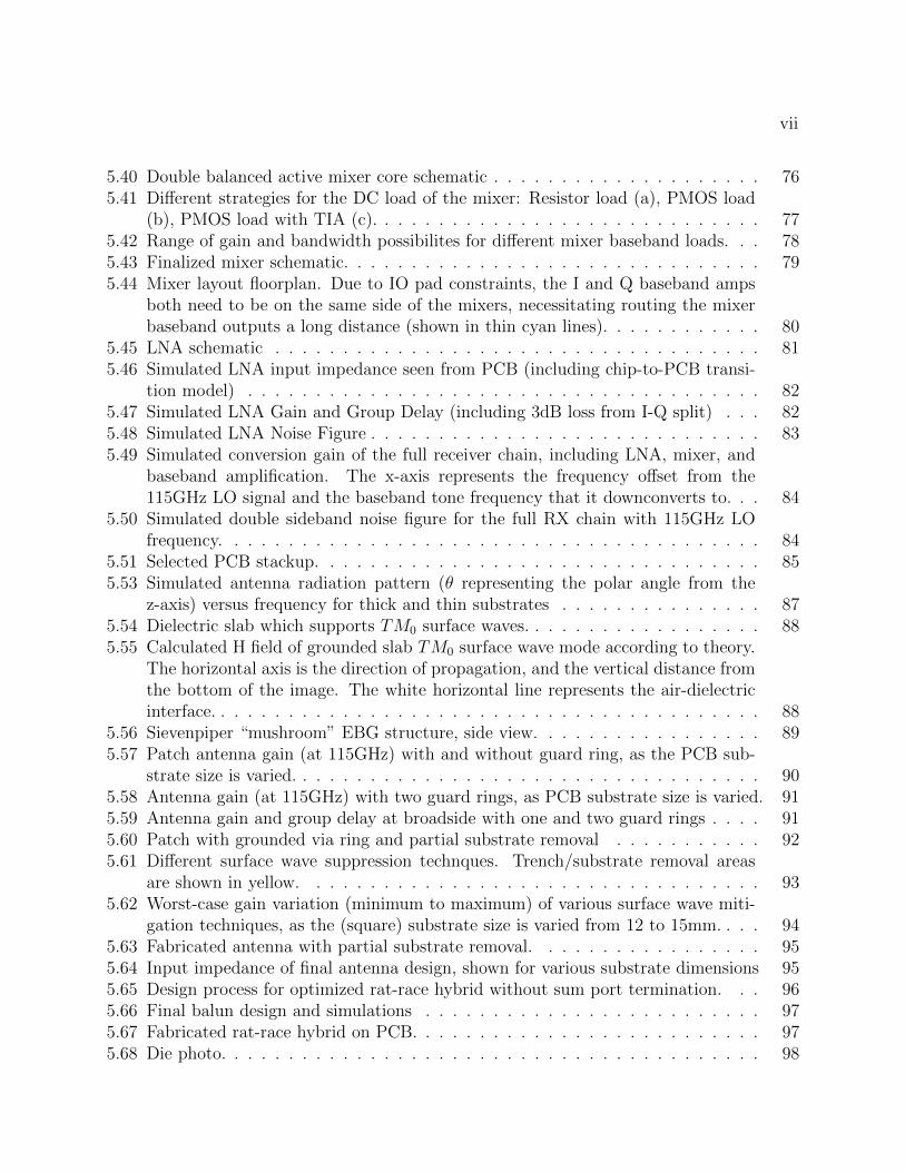
vii
5.40 Double balanced active mixer core schematic . . . . . . . . . . . . . . . . . . . . 765.41 Different strategies for the DC load of the mixer: Resistor load (a), PMOS load
(b), PMOS load with TIA (c). . . . . . . . . . . . . . . . . . . . . . . . . . . . . 775.42 Range of gain and bandwidth possibilites for different mixer baseband loads. . . 785.43 Finalized mixer schematic. . . . . . . . . . . . . . . . . . . . . . . . . . . . . . . 795.44 Mixer layout floorplan. Due to IO pad constraints, the I and Q baseband amps
both need to be on the same side of the mixers, necessitating routing the mixerbaseband outputs a long distance (shown in thin cyan lines). . . . . . . . . . . . 80
5.45 LNA schematic . . . . . . . . . . . . . . . . . . . . . . . . . . . . . . . . . . . . 815.46 Simulated LNA input impedance seen from PCB (including chip-to-PCB transi-
tion model) . . . . . . . . . . . . . . . . . . . . . . . . . . . . . . . . . . . . . . 825.47 Simulated LNA Gain and Group Delay (including 3dB loss from I-Q split) . . . 825.48 Simulated LNA Noise Figure . . . . . . . . . . . . . . . . . . . . . . . . . . . . . 835.49 Simulated conversion gain of the full receiver chain, including LNA, mixer, and
baseband amplification. The x-axis represents the frequency offset from the115GHz LO signal and the baseband tone frequency that it downconverts to. . . 84
5.50 Simulated double sideband noise figure for the full RX chain with 115GHz LOfrequency. . . . . . . . . . . . . . . . . . . . . . . . . . . . . . . . . . . . . . . . 84
5.51 Selected PCB stackup. . . . . . . . . . . . . . . . . . . . . . . . . . . . . . . . . 855.53 Simulated antenna radiation pattern (θ representing the polar angle from the
z-axis) versus frequency for thick and thin substrates . . . . . . . . . . . . . . . 875.54 Dielectric slab which supports TM0 surface waves. . . . . . . . . . . . . . . . . . 885.55 Calculated H field of grounded slab TM0 surface wave mode according to theory.
The horizontal axis is the direction of propagation, and the vertical distance fromthe bottom of the image. The white horizontal line represents the air-dielectricinterface. . . . . . . . . . . . . . . . . . . . . . . . . . . . . . . . . . . . . . . . . 88
5.56 Sievenpiper “mushroom” EBG structure, side view. . . . . . . . . . . . . . . . . 895.57 Patch antenna gain (at 115GHz) with and without guard ring, as the PCB sub-
strate size is varied. . . . . . . . . . . . . . . . . . . . . . . . . . . . . . . . . . . 905.58 Antenna gain (at 115GHz) with two guard rings, as PCB substrate size is varied. 915.59 Antenna gain and group delay at broadside with one and two guard rings . . . . 915.60 Patch with grounded via ring and partial substrate removal . . . . . . . . . . . 925.61 Different surface wave suppression technques. Trench/substrate removal areas
are shown in yellow. . . . . . . . . . . . . . . . . . . . . . . . . . . . . . . . . . 935.62 Worst-case gain variation (minimum to maximum) of various surface wave miti-
gation techniques, as the (square) substrate size is varied from 12 to 15mm. . . . 945.63 Fabricated antenna with partial substrate removal. . . . . . . . . . . . . . . . . 955.64 Input impedance of final antenna design, shown for various substrate dimensions 955.65 Design process for optimized rat-race hybrid without sum port termination. . . 965.66 Final balun design and simulations . . . . . . . . . . . . . . . . . . . . . . . . . 975.67 Fabricated rat-race hybrid on PCB. . . . . . . . . . . . . . . . . . . . . . . . . . 975.68 Die photo. . . . . . . . . . . . . . . . . . . . . . . . . . . . . . . . . . . . . . . . 98

viii
5.69 Flip-chip footprint, differential routing, and mm-Wave baluns as fabricated onPCB. . . . . . . . . . . . . . . . . . . . . . . . . . . . . . . . . . . . . . . . . . . 99
5.70 Antenna PCB with chip attached. . . . . . . . . . . . . . . . . . . . . . . . . . . 100

ix
List of Tables
4.1 Performance Comparison of Published W-Band Phased Array Transceivers . . . 38
5.1 Mapping from DAC bits to amplitude values . . . . . . . . . . . . . . . . . . . . 535.2 Characteristics of Various PCB Materials . . . . . . . . . . . . . . . . . . . . . . 865.3 Performance and Energy Efficiency of mm-Wave Wideband Transmitters . . . . 1015.4 Performance and Energy Efficiency of mm-Wave Wideband Receivers . . . . . . 101

x
Acknowledgments
First and foremost, I cannot thank my advisor Ali Niknejad enough for his technicaladvice and project guidance. I’ve had the luxury and flexibility of choosing my projectsthroughout most of my PhD, and I think few advisors would be willing to do that. It’sbeen fantastic to work for someone who has such a depth of technical expertise. Ali hasalso been a great advocate for my ambitious system-scale projects, and hopefully they willcontinue on in the center after I leave. I also want to thank Elad Alon who basically acted asan informal coadvisor during the design of the “Hummingbird” 120GHz chip, and providedmany valuable insights.
I had the benefit of having great lecturers for all of the courses I’ve taken at Berkeley,and thank Ali, Elad, Bernhard Boser, Simone Gambini, Bora Nikolic, Chris Hull, JosephOrenstein, and Martin White. Extra thanks to Elad, Bora, and Martin for serving on myquals committee and to Elad and Martin as readers for this thesis. Also an extra thanks toSimone, for helping me figure out what I wanted out of grad school over probably the mostimportant beer of my career.
I would like to thank Nokia Research / Nokia Labs for research funding and support onthe radar project, specifically Vason Srini and Klaus Doppler. I also appreciated the varioustechnical discussions I had during my internship with Michael Reiha and my fellow co-internPaul Swirhun. I owe many thanks to Paul for his design efforts on the phased-array radarIC. I also would like to thank the NSF-EARS program for its financial support for me andmy research. Thank you to the BWRC member companies and sponsors as well.
I also enjoyed my summer internships at Analog Devices and Google, and learned alot from them. Thanks to John Cowles, Todd Weigandt, Prabir Saha, Daryl Carbonari,Joel Dobler, Monica Cordrey, and Barrie Gilbert for a really enjoyable summer up in thenorthwest. And thank you to Ben Mossawir and Will Wesson for mentoring me during mysummer at Google.
In my (admittedly biased) opinion, BWRC is probably the best possible place in theuniverse to do a PhD in integrated circuits. A big part of that is the people. Firstly, Iwould like to thank all of the BWRC “senior students” who I have bugged over the yearswith various questions: Amin Arbabian, Jungdong Park, Jiashu Chen, Lingkai Kong, MattSpencer, Sahar Tabesh, Siva Thyagarajan, Shinwon Kang, Steven Callender, and Jun-ChauChien. I also really enjoyed all of the technical feedback, discussions, and collaborationswith my peers in the Niknejad and Alon groups. In particular, I would like to thank NathanNarevsky, Greg LaCaille, Luke Calderin, Constantine Sideris, Pramod Murali, Nai-ChungKuo, and Sashank Krishnamurthy. Costis and Sashank also contributed quite a bit to makingthe 120GHz transceiver a reality and it would not have been possible without them.
Over the years at BWRC, we have also had great support from the staff, and I would beremiss if I did not thank them profusely for all that they do for the center and its students.At the EE department level, I also really would like to thank Shirley Salanio for her tirelessefforts on keeping the entire department of grad students on track, myself included.

xi
I owe a big thanks to my research collaborators at the University of Nice Sophia Antipolisand STMicroelectronics: Cyril Luxey, Aimeric Bisognin, Diane Titz, Fred Gianesello, andRomain Pilard. I also really appreciate Cyril and Diane’s hospitality during my visit to Nicefor the radar active measurements, during a very difficult week for the city of Nice.
On a personal level, I want to thank my fellow Shattuck house roommates, for a reallyenjoyable five and a half years. Special thanks to Daniel Gerber, for reminding me howmuch I love the outdoors and many camping and climbing trips. And thanks to Joe Coreafor showing me the importance of having a good hobby or two (or three).
To Allison, thank you so much for your love, support, and understanding throughout thefinal years of my PhD, even when they took twice as long as I thought they would.
Finally, thank you to my parents for their support and encouragement, and for everythingyou have done for me that got me to this point. Thank you for cheering me on to the finishline from the other side of the country.

1
Chapter 1
Introduction
Since the introduction of digital wireless communication into the industrial and consumerspace, the evolution of wireless technology has been a self-reinforcing cycle, with each newgeneration of technology generating the demand for the next. Wireless LAN on laptops firstpaved the way for internet access without being tied to a desktop PC. This was followed bythe popularization of smartphones, which provided users wireless connectivity anywhere acellular connection could be found. In turn, the maturation of smartphone technology hastaken place alongside dramatic increases in cellular data capacity. Basic internet connectivityand picture sharing has been joined by video messaging and live streaming, and perhaps inthe near future will be joined by augmented or virtual reality.
To enable these developments to take place, wireless technology has had to advancecontinuously. But satisfying the demand for higher and higher wireless data rates, at somepoint, will inevitably be constrained by physical limitations. Once that happens, there arereally only two ways to improve the situation, according to Shannon’s capacity theorem [1]:
C = BW · log2
[1 +
S
N
](1.1)
When up against fundamental limits, either the signal-to-noise ratio or the signal band-width should be increased. Increasing signal-to-noise ratio allows for the use of more complexmodulation schemes, but requires a higher transmit power and/or a lower receiver noise levelto achieve. Because of the logarithm in the capacity equation, there are also diminishingreturns in increasing the SNR. For high SNR, a further doubling of SNR only leads to alinear increase in channel capacity. At some point, increasing the SNR becomes prohibitivefrom a DC power consumption point of view, or even simply impossible due to regulatoryconstraints on transmitted power level or interference from other users.
If that is the case, the only available route forward is to scale bandwidth. This, too,has costs when it comes to the physical implementation of the communication link. Trans-mitters, receivers, and antennas cannot be made arbitrarily broadband without taking someperformance hits (or causing significant headaches for the circuit, antenna, and system de-sign engineer). The performance hit (or the size of the engineer’s headache) is not related

CHAPTER 1. INTRODUCTION 2
THIS CHART WAS CREATED BY DELMON C. MORRISONJUNE 1, 2011
ISM – 24.125 ± 0.125 ISM – 5.8 ± .075 GHz3GHz
FIXE
D -
SATE
LLIT
E(E
arth-
to-sp
ace)
MOBI
LE -
SATE
LLIT
E(E
arth-
to-sp
ace)
Standard Frequency and
Time SignalSatellite
(space-to-Earth)
FIXE
DMO
BILE
RADI
OAS
TRON
OMY
SPAC
ERE
SEAR
CH
(pas
sive)
EART
HEX
PLOR
ATIO
N -
SATT
ELLIT
E (p
assiv
e)
RADI
ONAV
IGAT
ION
INTE
R-SA
TELL
ITE
RADI
ONAV
IGAT
ION
Radio
locat
ion
FIXE
D
FIXE
D
MOBI
LE
MobileFixed
BROA
DCAS
TING
MOBI
LE
SPAC
E RE
SEAR
CH
(pass
ive)
EART
H EX
PLOR
ATIO
N-SA
TELL
ITE (p
assiv
e)
SPAC
E RE
SEAR
CH (p
assiv
e)EA
RTH
EXPL
ORAT
ION-
SATE
LLIT
E (p
assiv
e)
EART
H EX
PLOR
ATIO
N-SA
TELL
ITE
(pas
sive)
SPAC
ERE
SEAR
CH(p
assiv
e)
MOBILE
FIXED
MOBILESATELLITE(space-to-
Earth)
MOBI
LE-
SATE
LLIT
ERA
DIO
NAVI
GATI
ONRA
DIO
NAVI
GATIO
N-SA
TELL
ITE
FIXED-SATELLITE(space-to-
Earth)
AMAT
EUR
AMAT
EUR-
SATE
LLIT
E
SPACERESEARCH
(passive)
RADIOASTRONOMY
EARTH EXPLORATION-
SATELLITE(passive)
MOBI
LEFI
XED
RADI
O-LO
CATI
ON
INTE
R-SA
TELL
ITE RADIO-
NAVIGATION
RADIO-NAVIGATION-
SATELLITE
AMAT
EUR
AMAT
EUR
- SAT
ELLI
TE
RADI
OLO
CATI
ON
EART
HEX
PLOR
ATIO
N-
SATE
LLIT
E (p
assiv
e)SP
ACE
RESE
ARCH
(pas
sive)SP
ACE
RESE
ARCH
(pas
sive)
RADI
OAS
TRON
OMY
MOBI
LEFI
XED
RADI
OAS
TRON
OMY
INTE
R-SA
TELL
ITE
RADI
ONAV
IGAT
ION
RADI
ONAV
IGAT
ION-
SATE
LLIT
E
SPACERESEARCH
(Passive)
RADI
OAS
TRON
OMY
EARTHEXPLORATION-
SATELLITE(Passive)
MOBI
LEFI
XED
MOBI
LEFI
XED
MOBILE
FIXED
FIXED-SATELLITE
(space-to-Earth)
RADI
OLOC
ATIO
NAM
ATEU
RAM
ATEU
R-SA
TELL
ITE
Amat
eur
Amat
eur-s
atell
ite
-NOITAROLPXE HTRAE SATE
LLIT
E (p
assiv
e)
MOBI
LE
SPAC
E RE
SEAR
CH(d
eep
spac
e) (s
pace
-to-E
arth)
MOBI
LE
MOBILE
SATELLITE
(space-to-Earth)
SPACE
RESEARCH
(Earth-to-space)
FIXED-SATELLITE
(space-to-Earth)
BROA
DCAS
TING
-SA
TELL
ITE
INTE
R- S
ATEL
LITE
EART
H EX
PLOR
ATIO
N-SA
TELL
ITE
(pas
sive)
SPAC
E RE
SEAR
CH
(pass
ive)
FIXE
DMO
BILE
**
SPAC
ERE
SEAR
CH(p
assiv
e)
EART
HEX
PLOR
ATIO
N-SA
TELL
ITE
(pas
sive)
RADI
ONAV
IGAT
ION
RADI
O-LO
CATI
ONSP
ACE
RESE
ARCH
(dee
p sp
ace)
(Ear
th-to-
spac
e)Ra
dio-
locat
ion
Spac
e res
earch
(dee
p sp
ace)
(Ear
th-to-
spac
e)
Radio
locat
ionRA
DIOL
OCAT
ION
EART
H
EXPL
ORAT
ION
-
SATT
ELLIT
E (a
ctive
)
RADIOLOCATION
SPACERESEARCH
(active)
Earth
explo
ratio
n -sa
ttellit
e (ac
tive)
Radiolocation
Spaceresearch (active)
EART
H EX
PLOR
ATIO
N -
SATE
LLIT
E(p
assiv
e)FI
XED
MOBI
LESP
ACE
RESE
ARCH
(p
assiv
e)
FIXE
DMO
BILE
FIXE
D-SA
TELL
ITE
(spa
ce-to
-Ear
th)
EART
H E
XPLO
RATI
ONSA
TELL
ITE
(Ear
th-to-
spac
e)
Earth
explo
ration
satel
lite(sp
ace-t
o-Eart
h)
FIXED-SATELLITE(space-to-Earth)
FIXEDMOBILE
BROA
DCAS
TING
-SA
TELL
ITE
BROA
DCAS
TING
FIXED
- SA
TELL
ITE(sp
ace-t
o-Eart
h)FI
XED
MOBI
LEBR
OADC
ASTI
NGBR
OADC
ASTI
NG S
ATEL
LITE
FIXE
DMO
BILE
**FIX
ED-SA
TELL
ITE(Ea
rth-to
-spac
e)RA
DIO
ASTR
ONOM
Y
FIXED
-SATE
LLITE
(Eart
h-to-s
pace
)MO
BILE
-SAT
ELLIT
E (E
arth-
to-sp
ace)
MOBI
LEMO
BILE
-SAT
ELLIT
E (E
arth-
to-sp
ace)
MOBI
LE-S
ATEL
LITE
(Ear
th-to-
spac
e)MO
BILE
FIXE
D
FIXE
DMO
BILE
FIXE
D-SA
TELL
ITE
(Ear
th-to-
spac
e)
FIXE
DMO
BILE
FIXE
D-SA
TELL
ITE
(Ear
th-to-
spac
e)
MOBI
LE-S
ATEL
LITE
(Ear
th-to-
spac
e)
FIXED
MOBILE
FIXE
D-SA
TELL
ITE
(Ear
th-to-
spac
e)
EART
H EX
PLOR
ATIO
N-SA
TELL
ITE
(pas
sive)
SPAC
E RE
SEAR
CH (p
assiv
e)
INTE
R- S
ATEL
LITE
INTE
R- S
ATEL
LITE
EART
H EX
PLOR
ATIO
N-SA
TELL
ITE
(pas
sive)
SPAC
E RE
SEAR
CH (p
assiv
e)
FIXED
MOBILE
EART
H EX
PLOR
ATIO
N-SA
TELL
ITE
(pas
sive)
SPAC
E RE
SEAR
CH (p
assiv
e)IN
TER-
SAT
ELLI
TE
FIXED
MOBILE
INTE
R- S
ATEL
LITE
EART
H EX
PLOR
ATIO
N-SA
TELL
ITE
(pas
sive)
SPAC
E RE
SEAR
CH (p
assiv
e)
MOBILE
FIXED
RADI
O-LO
CATI
ON
INTE
R- S
ATEL
LITE
FIXE
DMO
BILE
INTE
R- S
ATEL
LITE
INTE
R- S
ATEL
LITE
EART
H EX
PLOR
ATIO
N-SA
TELL
ITE
SPAC
E RE
SEAR
CH
FIXE
DMO
BILE
**
INTE
R- S
ATEL
LITE
MOBI
LE
BROA
DCAS
TING
FIXED- SATELLITE(space-to-
Earth)
Spaceresearch
(space-to-Earth)
MOBILE
Amat
eur
RADI
OAS
TRON
OMY
RADI
OLOC
ATIO
NSp
ace r
esea
rch(sp
ace-
to-Ea
rth)
Amat
eur
RADI
OLOC
ATIO
NSp
ace r
esea
rch(sp
ace-
to-Ea
rth)
AMAT
EUR
RADI
OLOC
ATIO
N
FIXED-SATELLITE
(Earth-to-space)
MOBILE-SATELLITE(Earth-to-space)
Spaceresearch
(space-to-Earth)
FIXED
MOBILE
FIXED-SATELLITE
(Earth-to-space)
FIXED
MOBILE
EARTHEXPLORATION-
SATELLITE(active)
SPACERESEARCH
(active)
RADIO-LOCATION
RADI
O-LO
CATI
ONMO
BILE
FIXE
D
FIXED
MOBILE
RADIOASTRONOMY
RADIO-LOCATION
RADIO-NAVIGATION
RADIO-NAVIGATION-
SATELLITE
RADI
OAS
TRON
OMY
SPAC
ERE
SEAR
CH(p
assiv
e)EA
RTH
EXPL
ORAT
ION-
SATE
LLIT
E (p
assiv
e)
SPAC
ERE
SEAR
CH(p
assiv
e)
FIXE
DMO
BILE
SPAC
ERE
SEAR
CH(p
assiv
e)
EART
HEX
PLOR
ATIO
N-SA
TELL
ITE
(pas
sive)
SPAC
ERE
SEAR
CH(p
assiv
e)EA
RTH
EXPL
ORAT
ION-
SATE
LLIT
E (p
assiv
e)
SPAC
ERE
SEAR
CH(p
assiv
e)IN
TER-
SATE
LLIT
E
FIXE
DMO
BILE
Amat
eur FIXED-
SATELLITE(space-to-Earth)
MOBILE-SATELLITE
(space-to-Earth)
Radioastronomy FIXED
MOBILE
INTER-SATELLITE
EART
HEX
PLOR
ATIO
N-SA
TELL
ITE
(acti
ve)
RADI
OAS
TRON
OMY
Radio
astro
nomy
Amat
eur -
sate
llite
Amat
eur
FIXE
DMO
BILE
RADI
O AS
TRON
OMY
SPAC
E RE
SEAR
CH(p
assiv
e)RA
DIO
ASTR
ONOM
YEA
RTH
EXPL
ORAT
ION-
SATE
LLIT
E (p
assiv
e)
FIXE
DMO
BILE
RADI
O AS
TRON
OMY
RADI
OLOC
ATIO
NEA
RTH
EXPL
ORAT
ION-
SATE
LLIT
E (p
assiv
e)
FIXED
RADI
O A
STRO
NOMY
FIXE
D-SA
TELL
ITE
(spac
e-to-
Earth
)
MOBI
LE-
SATE
LLIT
E(sp
ace-
to-Ea
rth)
FIXE
DMO
BILE
FIXE
DMO
BILE
FIXE
D-SA
TELL
ITE
(spac
e-to-
Earth
)
INTE
R-SA
TELL
ITE
EART
HEX
PLOR
ATIO
N-
SATE
LLIT
E (p
assiv
e)SP
ACE
RESE
ARCH
(pas
sive)
INTE
R-SA
TELL
ITE
SPAC
E RE
SEAR
CH(p
assiv
e)EA
RTH
EXPL
ORAT
ION-
SA
TELL
ITE
(pas
sive)
EART
HEX
PLOR
ATIO
N-
SATE
LLIT
E (p
assiv
e)IN
TER-
SATE
LLIT
ESP
ACE
RESE
ARCH
(pas
sive)
EART
H EX
PLOR
ATIO
N-
SATE
LLIT
E (p
assiv
e)SP
ACE
RESE
ARCH
(pas
sive)
FIXED
MOBILE
MOBI
LESA
TELL
ITE
INTE
R-SA
TELL
ITE
SPAC
E RE
SEAR
CH(p
assiv
e)EA
RTH
EXPL
ORAT
ION-
SA
TELL
ITE
(pas
sive)
RADI
OAS
TRON
OMY
FIXE
DMO
BILE
FIXE
D-SA
TELL
ITE
(Ear
th-to-
spac
e)
RADI
OAS
TRON
OMY
SPAC
E RE
SEAR
CH (p
assiv
e)
FIXED
FIXE
D-SA
TELL
ITE
(Ear
th-to-
spac
e)RA
DIO
ASTR
ONOM
Y
MOBILE
FIXE
DMO
BILE
FIXE
D-SA
TELL
ITE
(spac
e-to-
Earth
)
EART
HEX
PLOR
ATIO
N-
SATE
LLIT
E (p
assiv
e)SP
ACE
RESE
ARCH
(pas
sive)
FIXE
D-SA
TELL
ITE
(spac
e-to-
Earth
)
RADI
O-NA
VIGA
TION
RADI
O-NA
VIGA
TION
-SA
TELL
ITE
RADIO-LOCATION
RADI
OLOC
ATIO
NRA
DIOA
STRO
NOMY
Radio
astro
nomy
SPAC
E RE
SEAR
CH(p
assiv
e)RA
DIOA
STRO
NOMY
FIXED
MOBILE
MOBI
LE-S
ATEL
LITE
(Ear
th-to-
spac
e)RA
DIO
ASTR
ONOM
YRA
DION
AVIG
ATIO
N-SA
TELL
ITE
RADI
O NA
VIGA
TION
FIXE
DFIX
ED-S
ATEL
LITE
(Eart
h-to-s
pace
)NO
T ALL
OCAT
ED
MOBI
L-ES
ATEL
LITE
(spac
e-to-
Earth
)
RADI
OLOC
ATIO
N
RADI
OLOC
ATIO
N
MOBI
LEFI
XED-
SATE
LLIT
E(sp
ace-
to-Ea
rth)
Amat
eur
FIXE
DFI
XED-
SATE
LLIT
E(sp
ace-
to-Ea
rth)
MOBI
LE
MOBILE-
SATELLITE
(space-to-Earth)
MOBILE
FIXED
MOBI
LE
FIXED
FIXE
D
FIXE
D
30.0
31.0
31.3
31.8
32.3
33.0
33.4
34.2
34.7
35.5
36.0
37.0
37.5
38.0
38.6
39.5
40.0
40.5
41.0
42.0
42.5
43.5
45.5
46.9
47.0
47.2
48.2
50.2
50.4
51.4
52.6
54.25
55
.78
56.9
57.0
58.2
59.0
59.3
64.0
65.0
66.0
71.0
74.0
76.0
77.0
77.5
78.0
81.0
84.0
86.0
92.0
94.0
94.1
95.0
100.0
10
2.0
105.0
10
9.5
111.8
114.2
5 11
6.0
122.2
5 12
3.0
130.0
13
4.0
136.0
14
1.0
148.5
15
1.5
155.5
15
8.5
164.0
16
7.0
174.5
17
4.8
182.0
18
5.0
190.0
19
1.8
200.0
20
9.0
217.0
22
6.0
231.5
23
2.0
235.0
23
8.0
240.0
24
1.0
248.0
25
0.0
252.0
26
5.0
275.0
30
0.0
30GHz 300 GHz
Amateur
-sate
llite
Amateur
-satellite
Amateur
-satellite
RADIOASTRONOMY
RADIO
ASTRO
NOMY
RADIO
ASTRO
NOMY
RADIO
ASTRO
NOMY
BRO
ADCA
STIN
GSA
TELL
ITE
SPAC
E RE
SEAR
CH(sp
ace-
to-Ea
rth)
RADI
ONAV
IGAT
ION-
SATE
LLIT
ERA
DIO-
NAVI
GATI
ON-
SATE
LLIT
E
Spac
e res
earch
(spac
e-to-
Earth
)
Spac
e res
earch
(spac
e-to-
Earth
) RADIO
ASTRO
NOMY
RADIO
ASTRO
NOMY
RADI
OAS
TRON
OMY
MOBIL
E
FIXED
RADI
OLOC
ATIO
N
RADI
OAS
TRON
OMY
RADI
OAS
TRON
OMY
RADI
OAS
TRON
OMY MO
BILE
MOBI
LEFIX
ED FIXED
RADI
OAS
TRON
OMY
RADI
OAS
TRON
OMY
RADI
OAS
TRON
OMY
RADI
OAS
TRON
OMY Ra
dioloc
ation
Radio
locati
on
RADI
O AS
TRON
OMY
FIXE
D-SA
TELL
ITE
(spac
e-to-
Earth
)SP
ACE
RESE
ARCH
(spac
e-to-
Earth
)
Figure 1.1: United States Frequency Allocations Chart, 30–300GHz band.
to the absolute bandwidth required, but in fact the fractional bandwidth — the ratio of thebandwidth to the center frequency. It is quite difficult to design a 5 GHz carrier frequencywireless link with 5 GHz of bandwidth, while a link bandwidth of 5 GHz is readily achievableat 60GHz carrier frequency.
Shannon’s law does not say anything about the center frequency of the available chan-nel, so any 5 GHz chunk of spectrum is equally usable. But in order to more practicallyand efficiently take advantage of broad bandwidth channels, we need to operate at higherfrequency. This is the motivation behind operating circuits and systems in the so-called“millimeter-Wave” band.
Millimeter-Wave (mm-Wave) refers to radio frequencies with a wavelength of between 1and 10mm, or equivalently frequencies between 30 and 300GHz (Figure 1.1). Until fairlyrecently, this spectrum was limited to military and radioastronomy applications. However,in the last 15-20 years, there has been significant development of circuits and systems op-erating in the mm-Wave band. Initially, 60GHz-band wireless communications were thedriving force, culminating in the development of fully integrated transceivers supportinglarge antenna arrays, supporting up to 7Gb/s of peak data rate [2][3].
More recently, the major application driving mm-Wave development has been automo-tive radar [4][5][6]. Mm-Wave radar was initially proposed for driver-assist technologies suchas adaptive cruise control and lane change warning systems, which both require the highbandwidth available at mm-Wave frequencies for accurate distance resolution. Getting au-tomotive radar systems into the average car required driving the cost down, necessitatinga change from the very first modules using gallium-arsenide (GaAs) integrated circuits, tolower-cost silicon solutions. Fully integrated CMOS systems will soon be reaching the mar-ket [6], and as interest in fully autonomous vehicles continues to grow, development of thistechnology will accelerate further.
1.1 Motivation
The goal of this thesis is to explore the design tradeoffs and challenges in the design of broad-bandwidth millimeter-wave integrated transceivers, with an emphasis on the demonstrationof practical, complete systems. In this thesis, two transceiver designs are described, oneintended for mm-Wave short-range radar, and another for short-range communication. Dueto the complexity of routing signals on and off chip at millimeter-wave, it is also necessaryto consider the packaging and antenna design as part of the system design itself. Both

CHAPTER 1. INTRODUCTION 3
transceivers are integrated using flip-chip die attach technology directly onto the printedcircuit boards (PCBs) with included antennas.

4
Chapter 2
Millimeter-Wave Background
2.1 Technology: Bipolar vs MOSFET
A substantial amount of design work at millimeter-wave has been done using silicon germa-nium (SiGe) bipolar transistor technologies. These tend to be fairly inexpensive technologiesto use, since the critical dimension for high performance is the defined not by lithographybut by layer thickness (width of the base region of the bipolar transistor, in a conventionalvertical bipolar device). In addition to reduced fabrication mask cost, bipolar transistorsalso have a better gm
ICthan CMOS devices, and the gm efficiency is constant versus bias,
rather than trading off with fT as in CMOS.Modern bipolar process offerings do almost always include some CMOS transistors as well
— this type of process is referred to as SiGe BiCMOS — though the feature size is usuallyseveral process nodes behind the cutting edge [7][8]. Because of this, BiCMOS is best suitedfor analog-heavy applications such as power amplifiers [9], where low-speed digital circuitrymay sometimes be included but it is not critical to the performance of the system.
For digitally intensive circuits, CMOS clearly has the advantage. High data-rate digitaltransmitters have been demonstrated with intensive digital filtering while still maintaininghigh efficiency [10][11]. This certainly would not be possible using bipolar transistor logic,although it could perhaps be matched in performance with some efficiency cost using asufficiently finely scaled BiCMOS technology. Since SiGe BiCMOS scaling has not caughtup with pure CMOS scaling, it is not able to efficiently provide the high performance digitalfunctionality necessary to the operation of a complex mm-Wave system. CMOS is the defacto technology of choice for any millimeter-wave SoC intended for mass-market production[6].
As CMOS technology scales further into the FinFET regime, more challenges are in-troduced: thinner and more resistive routing layers, higher parasitic capacitances due tonon-planar device geometry, and stringent metal fill requirements. Initial investigationspublished in the literature suggest that these challenges can be overcome, and millimeterwave CMOS can still achieve high performance even scaled below 28nm [12]. Once FinFET

CHAPTER 2. MILLIMETER-WAVE BACKGROUND 5
processes become more widely available and the design challenges better understood, it ispossible that performance can be improved even further — the fT of FinFET devices insubthreshold operation may be sufficient to achieve high gain at millimeter wave, whichtranslates to an efficiency boost due to improved gm
ID.
2.2 LO Generation and Distribution
One of the most challenging aspects of generating an LO signal at millimeter-wave is de-signing a high-performance oscillator with wide tuning range. The poor analog varactor Qat high frequency degrades oscillator phase noise [13][14]. Therefore, it is advantageous togenerate the LO frequency at a lower frequency, and use a nonlinear frequency multiplier toscale it up by the desired amount.
In a multi-channel transceiver, where the LO signal is shared across multiple channels, atransmission-line-based routing network is usually required to keep impedances well-matchedover long distances. This can also be a source of high power consumption, since large LObuffers are required to drive the fairly low transmission line impedances that can be realizedon chip (which typically do not exceed 100Ω) without incurring high losses.
2.3 Modulation Techniques
2.3.1 Modulation Techniques for Radar
Of the various modulation schemes used for radar, all have the same main idea in common.A signal is transmitted with a known time-varying modulation, which reflects off of variousscatterers in the environment, and some small amount of energy is reflected back to thereceiver. Because the received signal is simply a time-delayed and attenuated version of thetransmitted signal, it can be compared with the known transmitted waveform to determinethe time delay. From the time delay, the round-trip distance is trivial to compute: d = c
td.
Also, because the transmitted signal and the received signal are both derived from thesame clock, their phase noise will largely cancel out. When the offset frequency of the phasenoise is equal to 1
Troundtrip, the phase noise will add coherently, and increase the noise floor
of the receiver. This is not as much of an issue for targets that are far away — the signalwill be heavily attenuated. The greatest concern is with high amplitude signals from nearbytargets. As these signals (often referred to as “clutter”) also tend to degrade the linearity ofthe receiver, it is obviously desirable to avoid them.
In practice, the transmitted signal tends to be periodic, which potentially introducessome ambiguity. If the period of the transmitted signal is T , then a given receive waveformcould correspond to a round-trip time delay of τ, τ+T, τ+2T, . . . For millimeter-Wave radar,this tends to not be an issue because the high signal attenuation tends to push the reflectedsignals from longer distances below the noise floor of the receiver.

CHAPTER 2. MILLIMETER-WAVE BACKGROUND 6
A critical parameter for the performance of a radar system is the bandwidth of the mod-ulated signal. In most types of radar system, the distance resolution is inversely proportionalto the bandwidth of the radar signal: a signal with larger bandwidth can better resolve twoclose-together targets [15]. This tradeoff is broadly applicable, since time (and therefore alsodistance, because of the constancy of the speed of light) and frequency are related by theFourier transform — a signal that is confined to a small region in time is necessarily broadin frequency space.
2.3.1.1 Pulse-Based Radar
Pulse-based radar is straightforward to understand: a short pulse is transmitted, the pulsereflects off of various objects in the environment, and a series of pulses is received corre-sponding to reflections from objects at different distances. The narrower the pulse, the moreaccurately closely spaced objects can be resolved. One nice feature is that the pulse neednot be detected coherently, since the information is contained only in the amplitude of thesignal. This approach is commonly used at optical frequencies in LiDAR (typically referredto as “time of flight” imaging) [16]. It has also been demonstrated in mm-Wave integratedcircuit form, with significant design effort required to ensure sufficiently narrow pulses [17].
2.3.1.2 Continuous Wave Radar
In contrast with pulse-based radar, continuous wave radar is always transmitting a signal.This presents significant challenges for the receiver, as it must either be carefully isolatedfrom the transmitter to avoid saturation at its output, or it must somehow tolerate the largetransmitter signal without compromising linearity and noise figure.
Continuous wave radar has no amplitude modulation, so in order to be able to measurerange, phase or frequency modulation must be added. Phase modulated continuous waveradar (PMCW radar) is attractive in that it can be implemented in an extremely simple andefficient manner, and orthogonal pseudo-random sequences can be used at different times toreduce the probability of inter-user interfence from multiple radar systems operating in closeproximity [18]. The bandwidth in a PMCW system is set by the sample rate at which thephase is modulated. Unfortunately, this also requires the same high bandwidth in the receiverbaseband amplification chain [18], which can become very challenging in high bandwidth /high resolution applications.
Frequency modulation, on the other hand, requires low baseband bandwidth [19][6], andlow instantaneous transceiver bandwidth. In a frequency modulated continuous wave radar(FMCW radar) system, high resolution still requires high bandwidth, but the bandwidthdoes not come from fast frequency steps. Instead, high bandwidth is achieved using a slow,smooth frequency ramp over multiple GHz. By removing the need for an instanenouslywideband signal, FMCW radar relaxes the specifications on the circuit design. This leads toa more efficient overall implementation.

CHAPTER 2. MILLIMETER-WAVE BACKGROUND 7
2.3.1.3 Advantages of Linear FMCW Radar for Millimeter-Wave
One specific type of FMCW waveform has some very desirable properties: linear FMCW.If the transmitted signal increases linearly in frequency, it can simply be mixed with thereceived reflected signal to yield an IF tone whose frequency is proportional to round-triptime delay [19]. Linear frequency modulated continuous wave (FMCW) radar is an attractiveradar modulation scheme for energy-efficient mm-wave applications for a few main reasons:constant-envelope and simplicity.
Firstly, because FMCW is a constant-envelope modulation scheme, transmitter linearityis not a concern. This allows for use of linear power amplifiers close to saturation, or evennonlinear switching power amplifiers, either of which will improve the overall transmitterefficiency. Also, because the modulated LO signal is constant-envelope, it can be generatedat a low frequency and scaled up to a higher frequency using a nonlinear frequency multipler,without negative impacts from the nonlinearity of the multiplier.
In a phased-array system, the modulated LO signal can be generated centrally, scaled infrequency, and routed out to all elements. As the LO routing network likely needed to bethere anyway, there is no penalty for doing this.
Secondly, because the modulation is simple and shared across all elements, the frequencymodulation can be incorporated into the PLL that is likely present in the system anyway. Fora pulsed radar system, a high-bandwidth modulation requires fast on/off times to achieve ashort pulse width [17], which means the circuit creating the modulation needs to be carefullydesigned to support that bandwidth. In a FMCW radar system, although large overallbandwidth is needed in the RF transmit and receive chains (as in the pulsed radar case), alarge instantaneous bandwidth is not necessarily needed, since it is the overall bandwidth ofthe sweep itself that determines the resolution. So, a slowly modulated signal can be used,as long as the frequency of the signal varies across the full bandwidth over time. Multipletargets at different distances correspond to multiple tones, and can be easily distinguishedby applying a Fourier transform to the received IF data.
2.3.2 Modulation Techniques for Digital Communication
The most basic modulation technique, and perhaps the first modulation technique to everbe used [20], is on-off keying. This simply consists of turning on and off the RF signal intime:
v(t) = A(t) cos(ωt) (2.1)
Where:
A(t) =∞∑
n=−∞
[u(t− nT )− u(t− (n+ 1)T )] a[n]
a[n] ∈ 0, 1
CHAPTER 2. MILLIMETER-WAVE BACKGROUND 8
and u(t) is the unit step function, which is used to mathematically model the zero-order holdinterpolation of the discrete-time digital data sequence a[n].
Note that this inherently assumes that the digital data is sampled at a regular intervalT . Since this waveform transmits one new bit of information every T seconds, we can saythat the data rate is 1/T bits/second.
2.3.2.1 Amplitude Modulation
To improve the data rate, instead of transmitting only a one or a zero, more signal levels canbe used to convey more information per bit period. For example, if there are four possiblesignal levels instead of two, log2(4) = 2 bits can be transmitted every T seconds. In thiscase, a[n] can take a broader range of values. If k bits per period are desired:
a[n] ∈
0,1
2k − 1,
2
2k − 1, . . . ,
2k − 2
2k − 1, 1
(2.2)
Without even doing any math, it’s obvious that there is a tradeoff for doing this: Shan-non’s equation (Equation 1.1) says that if the channel bandwidth is the same (which itapproximately is, if T is held constant), then the signal to noise ratio needs to increase inorder to provide increased capacity. So, in order to actually acheive the increase in datarate, we can deduce that the SNR has to increase proportionally.
2.3.2.2 Phase Modulation
Other than by changing the amplitude of a sinusoid, the only other way to send data is bymodulating the phase or frequency of the wave. In an analog communication system, theseare essentially the same thing: since frequency is the derivative of phase, in a continuous-timesystem it makes little difference for modulation and demodulation if the signal of interest isthe phase or its derivative. For a sampled, digital communication system, there is in fact ameaningful distinction, because the phase and frequency now have to change in discretizedsteps rather than smoothly.
Although it has been demonstrated at mm-Wave [21], digital frequency modulation suffersfrom poor bandwidth efficiency [22] and would be extremely challenging to implement in abroadband, coherent link. Because of this, mm-Wave transceivers generally have used almostexclusively phase modulation rather than frequency modulation.
The simplest version of phase modulation is binary phase shift keying (BPSK). Mathe-matically, this takes the form of a sinusoid that alternates between inverted and non-invertedphase.
v(t) = cos(ωt+ φ(t)) (2.3)
Where:
φ(t) =∞∑
n=−∞
[u(t− nT )− u(t− (n+ 1)T )]φ[n]

CHAPTER 2. MILLIMETER-WAVE BACKGROUND 9
φ[n] ∈ 0, πThe concept can be extended to k bits per symbol by increasing the number of possible
values that φ[n] can take:
φ[n] ∈
0,2π
2k, 2 · 2π
2k, . . . ,
(2k − 1
)· 2π
2k
This technique has the advantage of being constant envelope, which (as discussed in Sec-
tion 2.3.1.3) eases some implementation challenges arising from nonlinearity of the transmit-ter. Similarly to the amplitude modulation case, there is a tradeoff between SNR requirementand bandwidth efficiency of the modulation scheme.
2.3.2.3 Quadrature Amplitude Modulation
By applying both phase and amplitude modulation, arbitrary linear combinations of sine andcosine can be transmitted. One of the most useful implementations of that idea is known asquadrature amplitude modulation (QAM). In this modulation scheme, both sine and cosineare scaled independently by signed amplitude values.
Typically the case of interest is when sine and cosine share the same set of possibleamplitude values, that the amplitude levels are evenly spaced, and there are a power of twolevels in total (Equation 2.4, where k is the bits per symbol):
v(t) = I(t) cos(ωt) +Q(t) sin(ωt) (2.4)
Where:
I(t) =∞∑
n=−∞
[u(t− nT )− u(t− (n+ 1)T )] aI [n]
Q(t) =∞∑
n=−∞
[u(t− nT )− u(t− (n+ 1)T )] aQ[n]
aI [n], aQ[n] ∈−1,−2k/2 − 3
2k/2 − 1,−2k/2 − 5
2k/2 − 1, . . . ,− 1
2k/2 − 1,
1
2k/2 − 1, . . . ,
2k/2 − 5
2k/2 − 1,2k/2 − 3
2k/2 − 1, 1
In a completely linear system, it can be shown that for the same data rate, power level,
and bandwidth efficiency, QAM can provide the same bit error rate at lower SNR thanthe equivalent PSK modulation [22]. On the other hand, if the transmitter has strongnonlinearity, the variable amplitude levels of the QAM signal will be distorted. This lowersthe effective SNR at the receiver.
Due to the complexity in implementing PSK vs QAM at mm-Wave frequencies, QAMis used far more frequently. One exception is 4-QAM, which is also equivalent to 4-PSK(otherwise known as quadrature phase shift keying - QPSK).

CHAPTER 2. MILLIMETER-WAVE BACKGROUND 10
2.4 Phased Array Techniques
The main challenge in any mm-Wave system design is meeting link budget requirements, inlight of the large free space path loss at high frequencies. One way of efficiently addressing thelink budget problem is by leveraging phased-array techniques to reduce the total transceiverDC power [23]. For an N-element phased array, transmitter EIRP is increased by a factorof N2, since electric and magnetic fields, not power, are summed, and power density isproportional to ~E × ~H. Due to reciprocity, for the receiver array there will also be a benefitof N2 in conversion gain.
Receiver SNR will increase as well, but only proportional to N : since the noise in eachreceiver element is uncorrelated1, the total noise at the output will increase proportional toN , resulting in an SNR increase of N2/N = N . Because these system-level performancemetrics are improved in a phased-array compared to the single-element case, it is possible toreduce performance (and correspondingly, DC power) while still meeting system requirementsderived from the link budget.
Consider an RF power amplifier output stage, designed to operate close to saturation,and optimized to drive a load impedance of Z0. If the device sizes in the power amplifierare reduced by half, the power amplifier should be able to achieve the same efficiency atsaturation while driving a load impedance of 2Z0, and delivering half of the power to thatload. This scaled-down power amplifier can be used along with a matching network withan impedance transformation ratio of 2 (or if a matching network is already present, modi-fying its impedance transformation ratio) to drive the original load impedance of Z0, whiledelivering half of the power at the same efficiency. With a real matching network, there willbe some additional losses, so the efficiency and output power will in practice be degradedsomewhat. In a phased-array system, this strategy can be used to reduce DC power andper-element performance without sacrificing efficiency.
A similar scaling approach can be used on the receiver side. Consider an LNA designedfor power and noise matching to an impedance Z0. Because the current density for minimumnoise figure is largely invariant of emitter length [25] (or similarly, transistor width in CMOStechnologies), the LNA device sizes can be reduced by half, resulting in an LNA with thesame NFmin matched to an impedance of 2Z0. As in the transmitter case, a matchingnetwork can be used to match the LNA back to the original Z0 input impedance. The newLNA has half of the DC power consumption, and slightly higher noise figure due to the addedmatching network losses. Of course, due to matching network complexity, added losses, andthe bandwidth narrowing effect of high-Q matching networks, it is not possible to continuethis scaling arbitrarily. Architecture or circuit topology changes must then be used to reducepower consumption further.
1In general, correlated noise across receiver elements will mitigate some of this SNR improvement (referto [24] for a more detailed discussion). However, if the receiver elements are well isolated, and the noise ofthe combiner is small relative to the noise from the individual receivers, the factor of N scaling will hold.

11
Chapter 3
FMCW Radar Phased-ArrayTransceiver Design
Highly integrated millimeter-wave transceivers, enabled by advances in CMOS and SiGeBiCMOS process technology over the last decade, have found what is seemingly a perfectniche in automotive radar. With many GHz of absolute bandwidth available, and a compactantenna size due to the small wavelength at mm-wave, the W band matches up well with therequirements for adaptive cruise control and similar technologies [26]. The development ofmature, low-cost SiGe and CMOS technologies with ft and fmax of 150GHz and beyond hasbrought down the cost of such driver-assist technology and with it, widespread adoption.
More recently, mm-wave radar has also received increasing attention for short-range appli-cations such as gesture recognition, occupancy detection, and remote heart-rate monitoring[27][28][29][30][31]. However, existing mm-wave radar solutions intended for automotive useare power-hungry and often bulky. These drawbacks pose a problem for mobile, power-constrained applications. Towards this goal, in this work, a compact antenna-in-packageFMCW radar phased array solution at 94GHz with record-low per-element power consump-tion is proposed and demonstrated.
Although some promising progress has been made on gesture recognition radar at 60GHz[30],the higher frequency at 94GHz allows the possibility for larger sweep bandwidths (whichimproves depth resolution of the radar) and smaller antenna sizes. However, the higher fre-quency also presents a challenge from the circuit design point of view, which has a negativeimpact on efficiency and achievable SNR.
3.1 Proposed System Architecture
Several works have demonstrated state-of-the-art synthesizers with integrated frequencymodulation using a digital-PLL-based architecture [19][32][33][34]. The focus of this work ison energy-efficient array implementation and FMCW radar demonstration, so an externalsynthesizer is used to generate the frequency-modulated LO waveform. The chip includes

CHAPTER 3. FMCW RADAR PHASED-ARRAY TRANSCEIVER DESIGN 12
Á
Á
Á
Á
Á
Á
×2
÷32
vCtrl
47GHzVCOÁ
Á
λ/470.7Ω
λ/470.7Ω
λ/470.7Ω
λ/470.7Ω
λ/470.7Ω
λ/470.7Ω
λ/470.7Ω
λ/470.7Ω
λ/470.7Ω
λ/470.7Ω
λ/470.7Ω
λ/470.7Ω
vDiv
LNA1
LNA2
LNA3
LNA4
PA1
PA2
PA3
PA4
RX LOBuffer
TX LOBuffer
vIF1
vIFout
vIF1 vIF3
vIF2 vIF4
94GHz
47GHz
(1.47GHz)
vIF2
vIF3
vIF4
G
S
G
S
G
S
G
S
G
G
S
G
S
G
S
G
S
G
Figure 3.1: Complete phased-array transceiver block diagram. mm-wave IOs use a single-ended, ground-signal-ground (GSG) pad configuration. Ground pads are shared betweenadjacent phased-array elements to reduce die area.
a 47GHz VCO and 32× frequency divider, and the PLL feedback is completed externallyusing a discrete off-the-shelf IC with a phase-frequency detector (PFD) and charge pump,along with an on-board active loop filter. Most of the power consumption of the PLL islikely to come from the high-speed dividers, so if the PLL were fully integrated, the addedpower consumption would be fairly small and have little impact on the per-element power.
Because it is critical to minimize TX-RX leakage for an FMCW radar, an architecturewith separate TX and RX antennas was selected. Although it is possible to use an integratedisolating coupler to acheive some degree of isolation [35][36], even an ideal coupler will have3dB insertion loss due to the power-splitting nature of the coupler.
The block diagram of the full 4-TX, 4-RX phased array transceiver is shown in Figure3.1. To simplify routing in the antenna-in-package module, a small 4-element array sizewas selected, for both the transmit and receive arrays. LO generation circuitry is sharedbetween the transmit and receive elements, and consists of a VCO, frequency multiplier, andintegrated frequency dividers. A PLL was implemented off-chip for LO tuning and to enableFMCW ramp generation. A single, combined differential receiver output is fed off-chip.
For phase shifting, LO path phase shifters are used [37]. LO path phase shifting isattractive here because it removes phase shifter degradations such as nonlinearity and noisefrom the signal path. This increases efficiency because amplifiers on the LO path can bedesigned to operate close to compression, as the LO signal is constant envelope. Basebandphase shifting is also attractive from a power consumption perspective, but requires twomixers for complex downconversion. This is not necessary for a linear FMCW system; sincethe TX and RX frequencies are always slightly offset, the mixer strictly speaking is not truly

CHAPTER 3. FMCW RADAR PHASED-ARRAY TRANSCEIVER DESIGN 13
operating as a direct conversion mixer, and therefore power can be saved by only using asingle mixer.
3.2 Transmitter
To meet link budget requirements, a power amplifier was designed to provide approximately+9dBm of output power to a single-ended 50Ω antenna port. A single-ended antenna in-terface was selected to minimize mm-Wave IO count, which keeps the die area small andrelaxes routing constraints within the antenna module.
The main PA gain stage is based on a cascode amplifier. Because of the high outputimpedance of the cascode, it is hard to achieve a good power-added efficiency (PAE) usinga cascode output stage – the load-line impedance is significantly different from the small-signal impedance. However, the per-stage gain is still quite high relative to a simple commonemitter amplifier, which has high PAE, but low gain when driven close to saturation. Theamplifier core uses a differential topology to reduce sensitivity to modeling errors associatedwith the impedance seen at the cascode node. The bases of the cascode devices in a differ-ential pair can be shorted directly together using local routing only, and therefore present avirtual short circuit in differential mode. In common mode, gain is not a concern, so low-Qbypass capacitors are used to prevent any common-mode stability problems associated withthe impedance at the base of the cascode device.
To get both high gain and moderate efficiency, two cascode driver stages are used to drivea common-source output stage (see Fig. 5.30). A minimum supply voltage of 1.8V is neededto get good cacsode performance, but is slightly above the open-base VCE breakdown voltage
S
G
G1.8V
Vin
Q1(2μm)
R5=10Ω
Q1(2μm)
Q2(2μm)
Q2(2μm)
Q3(7μm)
Q3(7μm)
Q4(7μm)
Q4(7μm)
Q5(7μm)
Q5(7μm)
385pH
142pH
0.53
121pH
63pH
0.39
201pH
95pH
0.463.5mA1.8V
13.3mA1.8V
17.3mA13.5mA11.6mA3.4mA
Figure 3.2: Three-stage power amplifier schematic. R5 is chosen to result in an emittervoltage of about 100mV under small-signal bias conditions. The annotated DC currentscorrespond to the operating points in small-signal (left of arrow) and saturated large-signal(right of arrow) conditions.

CHAPTER 3. FMCW RADAR PHASED-ARRAY TRANSCEIVER DESIGN 14
of a single device. For the non-cascoded output stage, a moderate impedance is provided tothe base via the bias network to extend the VCE breakdown range beyond the open-base limitof BVCEO and allow operation from a single 1.8V PA supply [38]. For additional robustnessto VCE breakdown with the 1.8V supply voltage, a small series emitter degeneration resistoris added at the tail. This helps improve reliability issues and has no impact on gain since itappears only in common-mode.
It is difficult to power match at the output of the cascode due to the high real part of theoutput impedance, on the order of 1kΩ. Additionally, the real part of the input impedance ofthe cascode amplifiers is fairly small (tens of ohms), leading to a large required transformationratio. The available area for matching networks is constrained due to the phased-arrayelement pitch and the internal power-supply flip-chip bumps in between the phased-arraylanes, making it impossible to fit a transmission-line based matching network into the smallarea available for the PA. So, for a moderate impedance transformation ratio given the areaconstraints, coupling between PA gain stages is best achieved using 2:1 transformers withmoderate to low coupling factors.
Because of the low coupling factor, the effective turns ratio is slightly less than 2:1 inpractice, reducing the impedance transformation ratio. However, the leakage inductance ofthe transformer primary can be used to increase the impedance transformation ratio of thetransformer, by treating it as an additional inductance in series with the transformer, whichacts to increase the impedance seen at the ports of the primary transformer. The outputstage does not use neutralization because of the extra capacitive load it would present tothe output balun, which is also a 2:1 transformer. The output balun also provides ESDprotection to the signal pad, as at low frequencies it provides a low impedance path toground for the signal pads through the center tap of the secondary.
521μm
366μm
Figure 3.3: Full 3D EM model of PA interstage and output transformers.
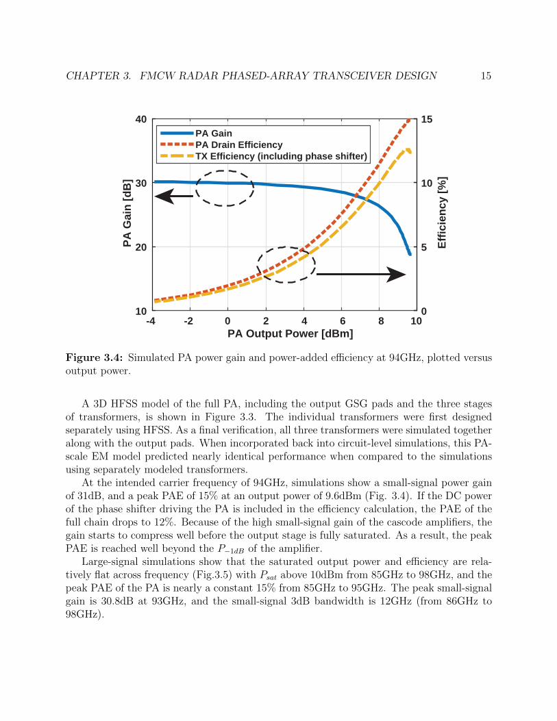
CHAPTER 3. FMCW RADAR PHASED-ARRAY TRANSCEIVER DESIGN 15
PA Output Power [dBm]-4 -2 0 2 4 6 8 10
PA G
ain
[dB
]
10
20
30
40
Effic
ienc
y [%
]
0
5
10
15PA GainPA Drain EfficiencyTX Efficiency (including phase shifter)
Figure 3.4: Simulated PA power gain and power-added efficiency at 94GHz, plotted versusoutput power.
A 3D HFSS model of the full PA, including the output GSG pads and the three stagesof transformers, is shown in Figure 3.3. The individual transformers were first designedseparately using HFSS. As a final verification, all three transformers were simulated togetheralong with the output pads. When incorporated back into circuit-level simulations, this PA-scale EM model predicted nearly identical performance when compared to the simulationsusing separately modeled transformers.
At the intended carrier frequency of 94GHz, simulations show a small-signal power gainof 31dB, and a peak PAE of 15% at an output power of 9.6dBm (Fig. 3.4). If the DC powerof the phase shifter driving the PA is included in the efficiency calculation, the PAE of thefull chain drops to 12%. Because of the high small-signal gain of the cascode amplifiers, thegain starts to compress well before the output stage is fully saturated. As a result, the peakPAE is reached well beyond the P−1dB of the amplifier.
Large-signal simulations show that the saturated output power and efficiency are rela-tively flat across frequency (Fig.3.5) with Psat above 10dBm from 85GHz to 98GHz, and thepeak PAE of the PA is nearly a constant 15% from 85GHz to 95GHz. The peak small-signalgain is 30.8dB at 93GHz, and the small-signal 3dB bandwidth is 12GHz (from 86GHz to98GHz).

CHAPTER 3. FMCW RADAR PHASED-ARRAY TRANSCEIVER DESIGN 16
Frequency [GHz]85 90 95 100 105
Pow
er [d
Bm
]
3
4
5
6
7
8
9
10
11
Psat Peak PAE Power Gain
Effic
ienc
y [%
], Po
wer
Gai
n [d
B]
0
5
10
15
20
25
30
35
40
Figure 3.5: Simulated PA saturated output power, power gain, and peak power-addedefficiency vs. frequency.
3.3 Phase Shifter
Passive reflection type phase shifters are an attractive option for low-power design, as theydo not consume any DC power and multiple stages can be cascaded to achieve the desiredphase-steering range [39][40]. However, this also implies the insertion loss trades off withphase shift range. To overcome this loss, an additional amplifier stage is needed, whichconsumes DC power.
Instead, in this design, a Cartesian architecture is used to ensure a full 360 degrees ofphase shift. Weighted combinations of the I and Q LO waveforms are current-combined atthe phase shifter output, meaning that the phase should be the same regardless of processvariations (provided the input quadrature matching is sufficiently accurate). The VGAfunctionality is achieved by current-steering using the cascode devices (Q5 through Q8)rather than the gm devices of the Gilbert cell. This ensures a more constant input impedancevs code. As the hybrid is single-ended, not differential, a balun stage is needed to drive thephase shifter LO inputs. A single-ended cascode amplifier with transformer load providessingle-ended to differential conversion, and further isolates the hybrid from any variations inphase-shifter input impedance.
3.3.0.1 Quadrature Coupler
The quadrature coupler is designed based on the approach in [41] to provide good phaseaccuracy over a broad bandwidth. It consists of three high-impedance transmission lines
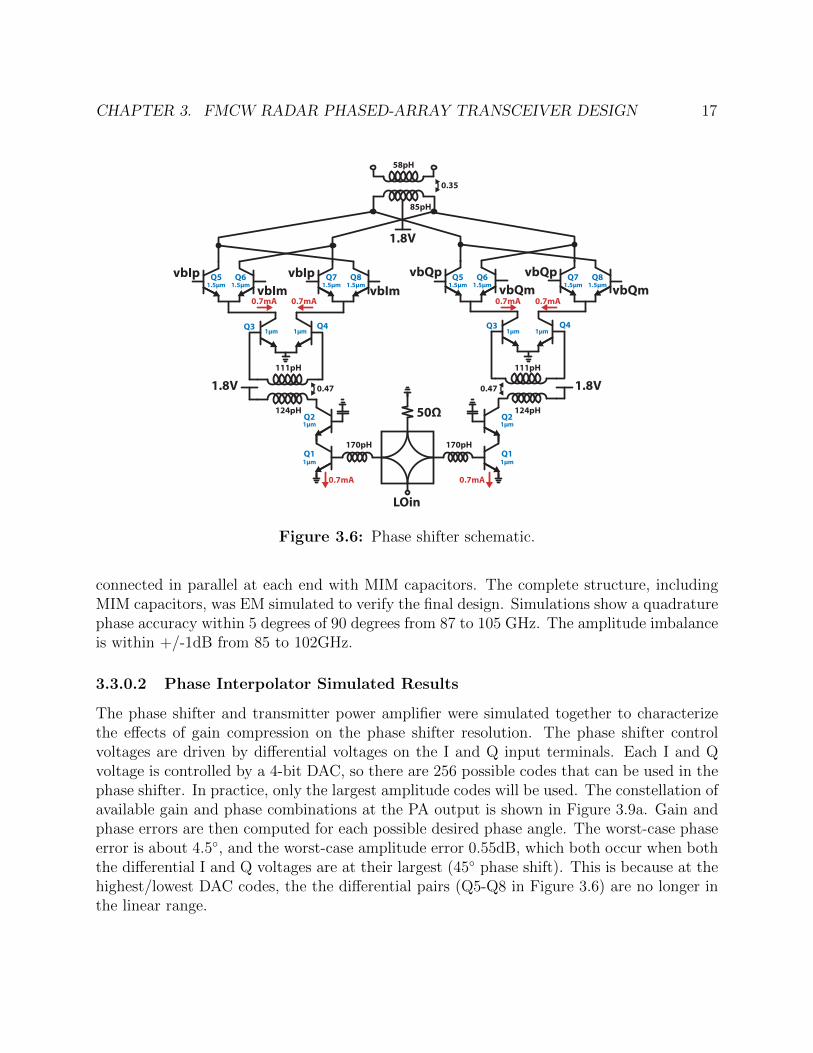
CHAPTER 3. FMCW RADAR PHASED-ARRAY TRANSCEIVER DESIGN 17
vbIp vbIpvbIm vbIm
vbQp vbQpvbQm vbQm
LOin
Q1
Q2
Q3 Q4
Q51.5μm
Q3 Q4
Q61.5μm
Q71.5μm
Q81.5μm
Q51.5μm
Q61.5μm
Q71.5μm
Q81.5μm
1μm 1μm 1μm 1μm
1μm
1μmQ1
Q21μm
1μm
170pH 170pH
124pH
111pH
124pH
111pH
0.47 0.47
50Ω
85pH
58pH
0.35
0.7mA0.7mA
0.7mA0.7mA 0.7mA0.7mA
1.8V1.8V
1.8V
Figure 3.6: Phase shifter schematic.
connected in parallel at each end with MIM capacitors. The complete structure, includingMIM capacitors, was EM simulated to verify the final design. Simulations show a quadraturephase accuracy within 5 degrees of 90 degrees from 87 to 105 GHz. The amplitude imbalanceis within +/-1dB from 85 to 102GHz.
3.3.0.2 Phase Interpolator Simulated Results
The phase shifter and transmitter power amplifier were simulated together to characterizethe effects of gain compression on the phase shifter resolution. The phase shifter controlvoltages are driven by differential voltages on the I and Q input terminals. Each I and Qvoltage is controlled by a 4-bit DAC, so there are 256 possible codes that can be used in thephase shifter. In practice, only the largest amplitude codes will be used. The constellation ofavailable gain and phase combinations at the PA output is shown in Figure 3.9a. Gain andphase errors are then computed for each possible desired phase angle. The worst-case phaseerror is about 4.5, and the worst-case amplitude error 0.55dB, which both occur when boththe differential I and Q voltages are at their largest (45 phase shift). This is because at thehighest/lowest DAC codes, the the differential pairs (Q5-Q8 in Figure 3.6) are no longer inthe linear range.

CHAPTER 3. FMCW RADAR PHASED-ARRAY TRANSCEIVER DESIGN 18
197μm
124μm
Figure 3.7: Quadrature hybrid HFSS model. The dimensions of the simulated region are197µm by 124µm.
Frequency [GHz]85 90 95 100 105
Phas
e D
ier
ence
[deg
rees
]
80°
85°
90°
95°
100°
Am
plitu
de d
ier
ence
[dB]
-2
-1
0
1
2
Figure 3.8: Quadrature hybrid simulated IQ mismatch.
3.4 LO Distribution
The LO generation circuitry includes an integrated VCO, frequency multiplier, frequencydividers, and LO buffers. The integrated VCO is designed to operate at half of the RFfrequency, and is buffered and sent to a frequency doubler to generate the RF carrier wave-form. The frequency-doubled LO waveform is buffered and distributed to the phased-arrayelements.
There is a routing penalty in distributing the LO signal after the frequency multipler,
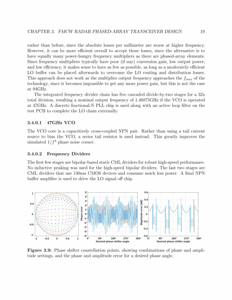
CHAPTER 3. FMCW RADAR PHASED-ARRAY TRANSCEIVER DESIGN 19
rather than before, since the absolute losses per millimeter are worse at higher frequency.However, it can be more efficient overall to accept those losses, since the alternative is tohave equally many power-hungry frequency multipliers as there are phased-array elements.Since frequency multipliers typically have poor (if any) conversion gain, low output power,and low efficiency, it makes sense to have as few as possible, as long as a moderately efficientLO buffer can be placed afterwards to overcome the LO routing and distribution losses.This approach does not work as the multiplier output frequency approaches the fmax of thetechnology, since it becomes impossible to get any more power gain, but this is not the caseat 94GHz.
The integrated frequency divider chain has five cascaded divide-by-two stages for a 32xtotal division, resulting a nominal output frequency of 1.46875GHz if the VCO is operatedat 47GHz. A discrete fractional-N PLL chip is used along with an active loop filter on thetest PCB to complete the LO chain externally.
3.4.0.1 47GHz VCO
The VCO core is a capacitively cross-coupled NPN pair. Rather than using a tail currentsource to bias the VCO, a series tail resistor is used instead. This greatly improves thesimulated 1/f 3 phase noise corner.
3.4.0.2 Frequency Dividers
The first few stages are bipolar-based static CML dividers for robust high-speed performance.No inductive peaking was used for the high-speed bipolar dividers. The last two stages areCML dividers that use 130nm CMOS devices and consume much less power. A final NPNbuffer amplifier is used to drive the LO signal off chip.
-1 -0.5 0 0.5 1-1
-0.5
0
0.5
1
Desired phase shifter angle180° 270° 360°
Phas
e er
ror
-5°-4°-3°-2°-1°0°1°2°3°4°5°
Mag
nitu
de e
rror
[dB
]
-0.6
-0.4
-0.2
0
0.2
0.4
0.6
0° 90°Desired phase shifter angle
180° 270° 360°0° 90°
Figure 3.9: Phase shifter constellation points, showing combinations of phase and ampli-tude settings, and the phase and amplitude error for a desired phase angle.

CHAPTER 3. FMCW RADAR PHASED-ARRAY TRANSCEIVER DESIGN 20
1.8V
1.2V supply (IDC=6.7mA)2.5V supply (IDC=39mA)
vb
CMOS÷2
CMOS÷2
1.8V
1.8V1.8V
1.8V
1.8V
R1=30Ω
2.05V
vCtrl
2.05V
to RXLO dist.
to TXLO dist.
BJT÷2
BJT÷2
BJT÷2
div.out
100pH
Le=16μmLe=16μm 1μm
1μm
123pH 111pH
0.41
R2=180Ω
300fF
2μm 2μm
60pHW/L=8×8μm/0.194μm
IDC(sim)=11.5mA
1.8V
L2=313pH
2.36mA (IDC)
2.36mA (IDC)
4.3mA
3.33mA (IDC)
8.7mA (IDC)
8.7mA (IDC)
0.8mA
1.4mA
Figure 3.10: Schematic of LO generation and distribution circuitry.
(a)
(b) (c)
Frequency [GHz ]20 60 100 140
Am
plitu
de [d
B]
-8.5
-8
-7.5
-7
-6.5
Outer portsInner ports
1.03mm
320μm
Figure 3.11: LO distribution network and power divider, based on lumped-element artificialtransmission line. Each artificial quarter-wavelength line consists of a 1.5 turn inductor inseries with a 1.25 turn inductor, which interfaces with a 50ohm transmission line.
CHAPTER 3. FMCW RADAR PHASED-ARRAY TRANSCEIVER DESIGN 21
3.4.0.3 Frequency Doubler
The frequency doubler uses a push-push topology with an inductive load [42]. A common-mode tail resistor is used instead of a current source, as simulations showed it provided slightenhancement of the 2nd harmonic output current. Simulations also indicated common-modestability problems when using a tail current source in the frequency doubler, related to thehigh-Q capacitance that it presents at the tail node, The common-mode stability issues areameliorated by using the tail resistor
3.4.0.4 LO Distribution Amplifiers
After the frequency doubler, the 94GHz LO waveform must be distributed to the TX andRX phased array elements. Separate distribution networks are used for the TX and RXelements, so that the power levels can be separately controlled. Even a lossless LO power-splitting network will inherently represent a reduction in power level, since the input poweris divided equally to all output paths. If LO buffers are used after the LO splitting network,the efficiency of any LO buffers will be quite poor, since the signal level will be very small dueto the splitting loss. To avoid suffering that efficiency penalty, moderate-power LO buffersare used drive the input of the power splitting network. This results in the same power levelsat the output, but a higher efficiency and reduced overall DC power.
The LO distribution amplifiers were designed by re-using the first PA gain stage (for bothamplifier stages of the LO buffers) and redesigning the interstage matching networks. Theoutput matching network is a transformer balun, to drive the single-ended LO distributionnetwork.
3.4.0.5 Lumped-Element Power Divider Network
To simplify the design of the divider network, two nested 1:2 power splitters are used. The 1:2splitter uses quarter wavelength Z0 = 70.7Ω lines to enable use in a cascade; when terminatedwith 50Ω loads, the input impedance of the splitter is also 50Ω. Typically, a Wilkinsonpower splitter is used as a 1:2 power splitter at millimeter wave [43]. The Wilkinson splitteris an isolating power divider, which will prevent potential crosstalk between elements. Adifferential-mode termination resistor is needed to provide this isolation, but requires thatthe outputs of the Wilkinson are physically close. Because the inputs of the phased-arraychannels are spaced apart by the array element pitch (300µm), additional routing is requiredto distribute the Wilkinson outputs to the phased-array elements (Figure 3.12a), whichrequires additional area and increases losses.
If a non-isolating network is used, it can also provide the required routing to the input ofeach array element (Figure 3.12b). Since the LO distribution network is terminated in thepassive quadrature hybrid load whose input impedance is constant vs phase code, there isno opportunity for crosstalk between elements even though a non-isolating splitter is used.
However, the splitter must fit within the array element pitch of 300µm, but the lengthof a single quarter-wavelength line on-chip is approximately 400µm. Clearly, a straight

CHAPTER 3. FMCW RADAR PHASED-ARRAY TRANSCEIVER DESIGN 22
300μm 300μm
(a) Isolating 2:1 splitter(Wilkinson) (b) Non-isolating 2:1 splitter
ℓ=λ/4Z0=70.7Ω
300μm
(c) Lumped-element-based non-isolating 2:1 splitter
ℓ(eff)=λ/4Z0(e)=70.7Ω
ℓ(eff)=λ/4Z0(e)=70.7Ω
ℓ=λ/4Z0=70.7Ω
ℓtotal=λ/4Z0=70.7Ω
Figure 3.12: Power splitter topologies considered for LO distribution.
1.8V
LO+ LO+LO- LO-
1.8V100Ω 100Ω
vIF1
S
G
G180fF
100Ω, λ/4(ESD)
R15Ω
Q2Q3 Q6Q4 Q5
Q13μm 3μm
180fF
74pH
40pH 111pH
82pH0.44
3μm 3μm 3μm 3μm
3.5mA 3.5mA 1.8V2.8mA
2.4mA 2.4mA
Figure 3.13: Receiver schematic.
transmission line will not be able to fit at this array element pitch - the transmission linewould need to be meandered to fit. Instead of using a meandered transmission line, thesplitter instead uses a lumped-element artificial transmission line to reduce the area of thenetwork (Figure 3.12c).
The insertion loss for an ideal 1 to 4 splitter would be 6dB - for this design, EM simulationsshow excess insertion losses of 7.1dB to 7.4dB (1.1 to 1.4dB higher than an ideal powersplitter) from 80-100GHz. The simulated amplitude mismatch is less than 0.04dB, with theouter ports receiving slightly more power than the inner ports, and less than 0.4 phasemismatch up to 100GHz.
3.5 Receiver
The number of LNA stages in the receiver was limited to keep DC power consumption low.Because of this, no inductive degeneration was used in the receiver input device (Q1 in Figure3.13), as this would reduce the gain of the LNA and increase the noise contribution of themixer to the overall receiver noise figure. Effectively, this means the input of the LNA is

CHAPTER 3. FMCW RADAR PHASED-ARRAY TRANSCEIVER DESIGN 23
0.2
0.5
1.0
2.0
5.0
+j0.2
-j0.2
+j0.5
-j0.5
+j1.0
-j1.0
+j2.0
-j2.0
+j5.0
-j5.0
0.0 ∞
(a) Adding series base inductor
0.2
0.5
1.0
2.0
5.0
+j0.2
-j0.2
+j0.5
-j0.5
+j1.0
-j1.0
+j2.0
-j2.0
+j5.0
-j5.0
0.0 ∞
(b) Adding series DC-blocking capacitor
0.2
0.5
1.0
2.0
5.0
+j0.2
-j0.2
+j0.5
-j0.5
+j1.0
-j1.0
+j2.0
-j2.0
+j5.0
-j5.0
0.0 ∞
(c) Adding shunt transmission line
Figure 3.14: Input impedance locus of the LNA, at various stages of the matching network.
designed for a power match, rather than a noise match. This adds a small amount (0.3dB)to the overall noise figure but limits the mixer noise figure contribution (see Fig. 3.17b).
Since the current density for minimum noise figure is typically 6-10 times smaller thanthe current density for peak fT [25], biasing for NFmin does have a gain penalty. As acompromise between gain and noise figure, the LNA input stage is biased at about half ofthe current density for peak fT . This leads to an increase of 0.5dB above the estimatedminimum noise figure of 3.2dB, but also allows the device to operate at nearly peak fT .
The input matching network uses a series inductor, a DC blocking capacitor, and aquarter-wavelength transmission line shunted to ground. Nearly all of the impedance match-ing is provided via the series base inductor. Because of the series inductor’s capacitance toground, it acts more like a transmission line than a simple series inductor. So, on a Smithchart, this looks like a rotation, rather than moving on a line of constant resistance (Figure3.14a). The DC-block capacitor is a small series impedance at RF and is only needed toseparate the bias points at the signal pad and LNA input (Figure 3.14b). The shunt trans-mission line provides a low-impedance path from the pad to ground at low frequencies forESD robustness, and contributes a small amount of shunt inductance at RF (Figure 3.14c).
The first LNA stage has an inductor load designed to resonate with its output capacitance,and is AC-coupled to the input of the second stage (Q2). The AC coupling capacitor betweenthe first and second stages is implemented using the standard MIM capacitor offered in theprocess. Its value is large so that it contributes a negligible series reactance, reducing designsensitivity to the modeling accuracy of the capacitor. The second LNA stage connects tothe differential mixer input using a transformer, which provides single-ended to differentialconversion.
The mixer itself is a double-balanced switching core (Q3-Q6), with RF signals coupledin at the emitters, and LO signals at the bases. Because headroom is limited, the mixeris implemented as a pseudo-differential rather than differential pair, and there is no RFtransconductor device in the mixer stack. The limited headroom also makes it difficult

CHAPTER 3. FMCW RADAR PHASED-ARRAY TRANSCEIVER DESIGN 24
553μm
420μm
Figure 3.15: Receiver HFSS model.
LO frequency [GHz]85 90 95 100 105
Conv
ersi
on g
ain
[dB]
20
25
30
35
40
85 90 95 100 105
Noi
se
gure
[dB]
11
11.5
12
12.5
LO frequency [GHz]
Figure 3.16: Simulated receiver conversion gain and noise figure vs mixer LO frequency,for all 5 gain control settings.
to use a high-impedance active load that is sufficiently saturated. A resistive load is usedinstead, largely to set the bias point, and a transimpedance amplifier (TIA) is used to providea low impedance at the mixer baseband output. Using this topology we are able to improvethe voltage gain of the mixer, while the headroom is constrained. Additionally, the resistiveload has improved noise performance over the active load, and suffers from less capacitiveparasitics: the PMOS ft is low relative to that of the NPN devices, and no high-speed PNPis available in this technology. Gain control is achieved by varying the feedback resistancein the baseband TIA via switched resistor segments. The TIA itself consists of a high-speedop-amp using SiGe NPN devices.

CHAPTER 3. FMCW RADAR PHASED-ARRAY TRANSCEIVER DESIGN 25
+j10Ω
-j10Ω
+j25Ω
-j25Ω
+j50Ω
-j50Ω
+j100Ω
-j100Ω
+j250Ω
-j250Ω
0.0Ω ∞
+0.5dB circle
+0.3dB circle
+0.1dB circle
6%port noise @ 94GHz - Δf
22%LNA 1st stage noise @ 94GHz - Δf
5%LNA 2nd stage noise @ 94GHz - Δf
9%mixer noise @ 94GHz - Δf
6%port noise @ 94GHz + Δf
22%LNA 1st stage noise @ 94GHz + Δf
5%LNA 2nd stage noise @ 94GHz + Δf
9%mixer noise @ 94GHz + Δf
12%mixer noise @ Δf
6%Op-amp noise @ Δf
(a) (b)
10Ω
25Ω
50Ω
100Ω
250Ω
Figure 3.17: (a) Percentage contributions of different blocks to total output noise. Thecontributions are separated by sideband. (b) Noise circles
Gai
n [d
Bi]
Gai
n [d
Bi]
-10
-5
0
5
10
15
Main lobe levelGrating lobe level
Frequency [GHz]90 92 94 96 98 100
Coup
ling
Am
plitu
de [d
B]
-90
-80
-70
-60
-50
Angle relative to broadside-90° -60° -30° +30° +60° +90°0°
Desired beam angle (rel. to broadside)0° 10° 20° 30° 40°
-10
-5
0
5
10
15
12dB6.6dB
(a) Radiation pattern at variousbeam steering angles
(b) Main and grating lobe levelsversus desired beam angle
(c) Simulated TX-RX coupling
Figure 3.18: HFSS simulations of antenna module.
Simulations show a receiver conversion gain of 25-38dB and a noise figure ranging from11.1 to 11.3dB (single-sideband) at 94GHz, depending on gain control settings. Since thegain control is implemented at the IF amplification stage, it has little impact on noise figurebecause of the front-end gain in the preceding stages. As can be seen in Figure 3.17a,approximately 54% of the total noise at the receiver output is due to the LNA, 30% from themixer, 6% from the baseband amplification, and 12% from the reference noise of the inputport.
3.6 Packaging
The die was flip-chip packaged using stud bumps onto an antenna module fabricated usingan organic HDI substrate [44]. The antenna module is based on a standard BGA footprint

CHAPTER 3. FMCW RADAR PHASED-ARRAY TRANSCEIVER DESIGN 26
(a)
(b)
(c)
Figure 3.19: Levels of integration of radar IC. Bare die (a) is flip-chip chip packaged ontoBGA antenna module (b), which is integrated onto a test PCB (c). The test PCB is 10.2cmx 10.2cm, sized to accomodate connectors to a separate FPGA board. If a microcontrollerwere used instead of an FPGA, the board area could be reduced to a much smaller size.
and low-frequency connections fan out to BGA balls for integration onto a larger test PCB(Figure 3.19). The substrate, 1.2cm by 1.2cm, contains two linear arrays of 4 patches each -one array for the transmitter elements and one array for the receiver elements. For high TXto RX isolation, the TX and RX antenna arrays are located on opposite sides of the module.The antennas themselves are aperture-coupled patch antennas with linear polarization. Toreduce element-to-element coupling, the antenna spacing within each array is set to 0.8λ at94GHz.
Because the antenna spacing is greater than half-wavelength, grating lobes will appearfor large beam-steering angles. HFSS simulations of the antenna array predict that a beam-steering range of ±27 is possible for a grating lobe level of 3dB below the main lobe (Figure3.18). At a simulated beam-steering angle of ±34, the grating lobe level is the same as thatof the main lobe. The simulated 3dB beam width of the main beam is about 16 in the E
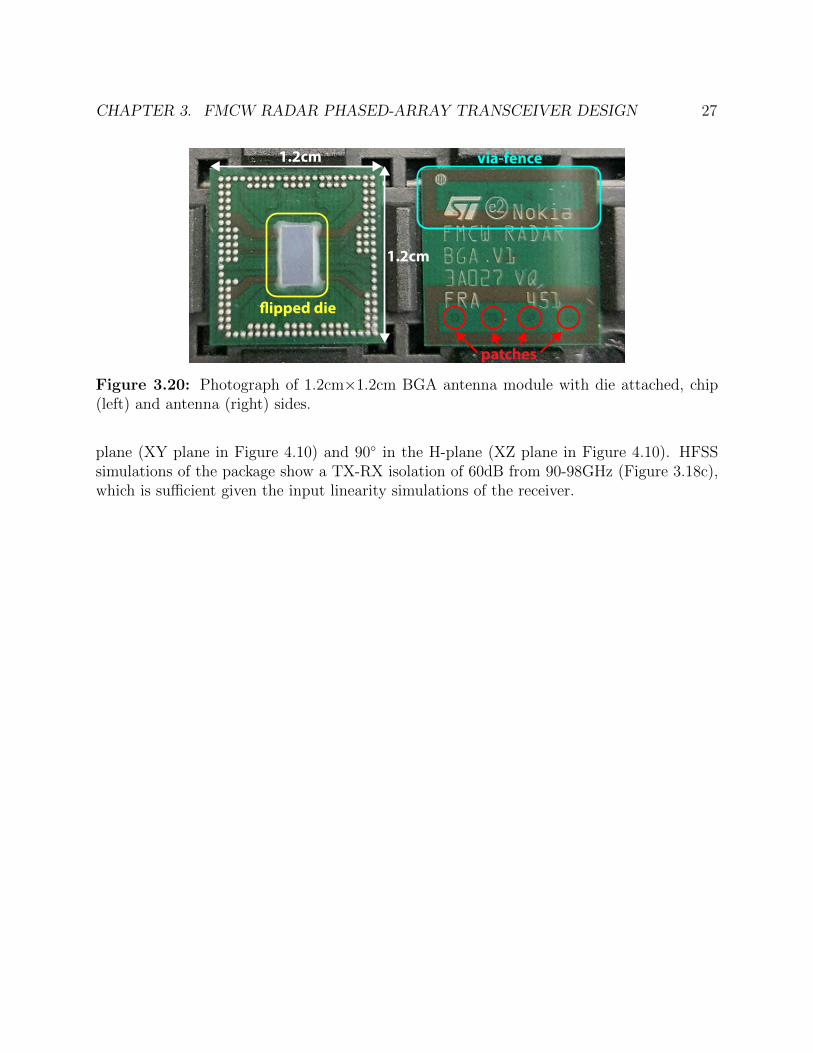
CHAPTER 3. FMCW RADAR PHASED-ARRAY TRANSCEIVER DESIGN 27
patches
via-fence
ipped die
1.2cm
1.2cm
Figure 3.20: Photograph of 1.2cm×1.2cm BGA antenna module with die attached, chip(left) and antenna (right) sides.
plane (XY plane in Figure 4.10) and 90 in the H-plane (XZ plane in Figure 4.10). HFSSsimulations of the package show a TX-RX isolation of 60dB from 90-98GHz (Figure 3.18c),which is sufficient given the input linearity simulations of the receiver.

28
Chapter 4
Radar IC Measurements
The 3.7x2.2mm chip was fabricated in a 130nm SiGe BiCMOS process (Fig. 4.1). The TXand RX arrays are on opposite sides of the chip. At the TX and RX arrays, the ground-signal-ground mm-Wave IO pads are placed vertically running up the sides of the chip. Adjacentground pads are shared between elements to reduce die size. Shared LO generation circuitryis at the center of the chip and feeds in to the power divider networks, which in turn feeddirectly in to the phase shifters for the transmitters and receivers. The chip was tested bothusing mm-wave probes in a chip-on-board configuration, and using the packaged antennamodule for wireless measurements.
Figure 4.1: Die photograph of fabricated chip.

CHAPTER 4. RADAR IC MEASUREMENTS 29
4.1 Probe Station Measurements
4.1.1 LO
The measured VCO tuning range is 11%, from 44 to 49GHz . The VCO center frequencyis about 5% lower than simulated, but due to the large designed tuning range it still coversthe desired center frequency of 47GHz. The PLL locking range is from 89-95GHz, slightlyreduced from the VCO tuning range. It is limited by kV CO at low tuning voltages, and bythe output swing of the active loop filter at high tuning voltages. At 94GHz, the closed-loopphase noise is -76dBc/Hz at 1MHz offset, measured at the PA output .
Tuning voltage [V]0 1 2 3
VCO
freq
uenc
y [G
Hz]
43
44
45
46
47
48
49
Oset Frequency [Hz]10 5 10 6 10 7 10 8
Phas
e no
ise
[dBc
/Hz]
-120
-100
-80
-60
-40
(a) (b)
LO fr
eque
ncy
[GH
z]
86
88
90
92
94
96
98
PLLlock
range
Figure 4.2: VCO tuning curve, and measured phase noise of PLL at 94GHz.
4.1.2 Transmitter
Probe station measurements were used to characterize the output power of individual PAs,along with a W-band power meter. At 94GHz, the output power varies over a range of about0.5dB across elements, from 6.3dBm to 6.8dBm . The outer TX elements (1 and 4) have thehighest output power, and the inner elements have lower output power. The output powerwas lower than the simulated Psat = +10.5dBm of the PA, as well as the simulated +9dBmoutput power with expected LO signal levels. The decrease in output power for inner TXelements suggests IR drop in the supply network may be a partial cause. Additionally, theoutput power decreases beyond 90GHz, whereas in simulations, it decreased after about94GHz. Unfortunately, due to the integrated LO chain and limited VCO tuning range, it isnot possible to measure outside of the 89-95GHz frequency range, so it cannot be verifiedif the output power increases further at lower frequencies. The decreased output power,and trend of power vs PA element, was consistently observed across multiple chips. Themeasured PA output impedance matches closely with simulation (Fig. 4.4b). The averageoutput power of 6.5dBm results in a transmitter efficiency of 6.3% (PTX,RF/PTX,DC)

CHAPTER 4. RADAR IC MEASUREMENTS 30
Frequency [GHz]89 90 91 92 93 94 95
Out
put P
ower
[dBm
]
5.5
6
6.5
7
7.5
8
Elem. 1Elem. 2Elem. 3Elem. 4
Figure 4.3: Measured transmitter output power vs frequency.
100Ω
250Ω
+j10Ω
-j10Ω
+j25Ω
-j25Ω
+j50Ω
-j50Ω
+j100Ω
-j100Ω
+j250Ω
-j250Ω
0 ∞
(a) LNA input impedance
SimulatedMeasured
10Ω
20Ω
50Ω
(b) PA output impedance
SimulatedMeasured
100Ω
250Ω
+j10Ω
-j10Ω
+j25Ω
-j25Ω
+j50Ω
-j50Ω
+j100Ω
-j100Ω
+j250Ω
-j250Ω
0 ∞10Ω
20Ω
50Ω
Figure 4.4: The measured LNA input impedance (a) and PA output impedance (b) showedgood agreement with simulation.
4.1.3 Receiver
The receiver noise figure was measured with the hot/cold method, using an Agilent N8974Anoise figure meter and W-band WR-10 noise source, connected to the receiver input via aW-band GSG probe (Fig. 4.5). In the RX case, element-to-element mismatch in noise figure

CHAPTER 4. RADAR IC MEASUREMENTS 31
is quite small. We do not see a consistent trend of increased noise figure in the interiorelements, which makes sense because noise figure should not be as sensitive to IR drop. Wealso see that the RX noise figure is improving vs frequency, unlike in the TX case wherethe best performance was at lower frequency. The measured 12.5dB (SSB) noise figure at94GHz is higher than the simulated 11.1dB (SSB) at 94GHz. Below 94GHz, the noise figureincreases quite drastically. This is potentially due to insufficient LO power at the RX mixer,as the LO distribution network is tuned slightly high due to EM modeling error and itsoutput power drops off below 93GHz. The measured LNA impedance matches somewhatclosely with simulation, although detuned slightly (Fig. 4.4a). The measured P1dB of thereceiver is -19dBm at 94GHz.
Frequency [GHz]89 90 91 92 93 94 95
Noi
se F
igur
e [d
B]
12
12.5
13
13.5
14
14.5
15Elem. 1Elem. 2Elem. 3Elem. 4
Figure 4.5: Measured receiver single-sideband noise figure (probe station) vs frequency.
4.2 Packaged Measurements
4.2.1 Array Characterization
Initial measurements of the phased array were performed at broadside, with zero phase shiftbetween elements, to verify that transmitter spatial combining works as expected. EIRPmeasurements of the transmit array at broadside (Fig 4.6) indicate an EIRP of approximately+22dBm at 94GHz. The measured EIRP roughly increases by 6dB when the number ofenabled PAs is doubled, which is consistent with the theoretical N2 factor for in-phasespatial combining.
To further demonstrate phased array operation, the TX radiation pattern was measuredat various beam steering angles. First, the TX radiation pattern was characterized in the labat BWRC, by using a W-band power meter head (connected to a horn antenna) manually

CHAPTER 4. RADAR IC MEASUREMENTS 32
Frequency [GHz]89 90 91 92 93 94 95
EIR
P [d
Bm]
0
5
10
15
20
25
All PAs on2 PAs on1 PA on
Figure 4.6: EIRP at broadside vs frequency, for 1, 2, and 4 PAs enabled. All possiblecombinations of the 1 and 2 PA cases are plotted.
placed at different angles relative to the broadside of the array. Because the measurementwas done manually, the measurements points are in 5 increments, over a range of -60 to60 from the broadside of the array (Figure 4.7).
The RX conversion gain pattern was also characterized using a similar approach, butinstead using a 94GHz source and horn antenna placed at various angles, instead of thepower meter. Similarly to the case of the TX EIRP, the conversion gain roughly increasesby 6dB when the number of enabled LNAs is doubled.
However, for both the RX and TX cases, this improvised setup led to very slow measure-ments, required manual intervention to move the power meter or source from angle to angle,and was only capable of doing measurements along a single cut plane.
An indirect phase shifter characterization was completed based on beamforming andpower-combining measurements at different phase shifter codes (Fig. 4.9). Because the PAis not fully driven into saturation, amplitude error is not suppressed. The measured peakphase and amplitude error are 9 degrees and 1.4dB, respectively.
The TX radiation pattern was also characterized at University of Nice Sophia-Antipolis(UNS), using the measurement setup first described in [45] and extended to 90-140GHz in[46] (see Fig. 4.10a). The digitally controllable arm can move along both φ and θ angles, soit is possible to capture nearly a full hemisphere of the radiation pattern with single-degree-level steps. An F-band subharmonic mixer is placed on the end of the moveable arm and theIF output connected to a spectrum analyzer. The power level is measured by observing the

CHAPTER 4. RADAR IC MEASUREMENTS 33
angle rel. to normal [deg]-60 -40 -20
rela
tive
pow
er [d
B]
-25
-20
-15
-10
-5
0
0 20 40 60
Figure 4.7: Beam steering of transmitter at 94GHz, characterized manually at BWRC.
Frequency [GHz]89 90 91 92 93 94 95
RX
arra
y co
nver
sion
gai
n [d
B]
15
20
25
30
35All LNAs on2 LNAs on1 LNA on
Figure 4.8: RX array conversion gain vs frequency, for 1, 2, and 4 LNAs enabled. Allpossible combinations of the 1 and 2 LNA cases are plotted.
peak level of the downconverted signal level on the spectrum analyzer. Due to the large sizeof the F-band signal source, it was not possible to mount the signal source on the moveablearm to measure the RX beam steering pattern. However, the results should be similar as

CHAPTER 4. RADAR IC MEASUREMENTS 34
-1 -0.5 0 0.5 1-1
-0.5
0
0.5
1
Figure 4.9: Measured phase shifter constellation points, with circle showing amplitude levelwith least average amplitude error.
X
Y
ZZ
Y
XY
Z
(a) (b) (c)
Θ
Á
Figure 4.10: The measurement setup at University of Nice-Sophia Antipolis. The test PCBis placed with the radiating side downward, and the arm with the receive antenna is sweptacross phi and theta angles. The measured radiation pattern data is imported into HFSSand plotted. The axes shown in (a) correspond to the axes in the HFSS plots (subfigures band c)

CHAPTER 4. RADAR IC MEASUREMENTS 35
0° -10° -20°
20.0dBm16.4dBm12.9dBm9.3dBm5.7dBm2.1dBm-1.4dBm-5.0dBm
EIRPZ
Y
Z Z
Y
Z
Y
Z
Y
Z
Y
30° 20° 10°
Y
Figure 4.11: 3D radiation pattern measurements at various beam steering angles (per-formed at UNS).
the antenna arrays and phase shifters are identical for both the TX and RX.The measured 3D radiation pattern for various beam steering angles is plotted in Figure
4.11. Similar to the HFSS simulations of the array, there are significant side lobes at the30 beam steering angle. The beamforming measurements show a steering range of about±20 degrees while maintaining 3dB main lobe to grating lobe levels. The beam drop-off isabout 2-3dB at +20 and 4 dB at -20(Figure 4.12). This is slightly worse than predictedby HFSS simulations of the antenna array, which showed only 1 to 1.5dB of beam drop off.Measurements along the E-plane of the array show little variation in radiation pattern versusbeam steering angle (Figure 4.13).
4.2.2 Radar Measurements and Characterization
As a basic demonstration of radar capability, a simple experiment was performed using ametal reflector at different distances. A triangular frequency modulation was applied tothe reference signal of the PLL, with both 4% and 2% sweep bandwidths. At 4% sweepbandwidth (3.68GHz RF bandwidth), the FFT of the IF waveform shows distinct peaksin different range bins when the object is moved by 5cm (Figure 4.14a). At 2% sweepbandwidth (1.86GHz RF bandwidth; for the 2% sweep, the center frequency was retunedslightly higher), the peaks are still present, but in some cases the reflected signal occupiesmultiple range bins (Figure 4.14b). According to the range resolution equation, there should
be a range resolution ofc
2B=4.1cm in the 4% sweep case, and 8.1cm in the 2% sweep case.
This is consistent with the measured results of the radar experiment.
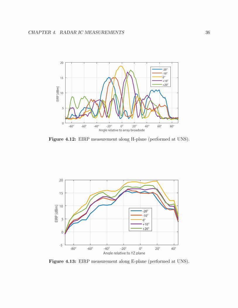
CHAPTER 4. RADAR IC MEASUREMENTS 36
Angle relative to array broadside-80° -60° -40° -20°
EIRP
[dBm
]
0
5
10
15
20
-20°-10°0°+10°+20°
0° 20° 40° 60° 80°
Figure 4.12: EIRP measurement along H-plane (performed at UNS).
Angle relative to YZ plane-80° -60° -40° -20°
EIRP
[dBm
]
-5
0
5
10
15
20
-20°-10°0°+10°+20°
0° 20° 40°
Figure 4.13: EIRP measurement along E-plane (performed at UNS).

CHAPTER 4. RADAR IC MEASUREMENTS 37
d [cm]20 30 40 50 60 70
RX s
igna
l lev
el [d
B]
-20
-10
0
10
20
30(a) 3.68GHz sweep bandwidth
d = 35.6cmd = 40.6cmd = 45.7cm
d [cm]20 30 40 50 60 70
RX s
igna
l lev
el [d
B]
-20
-10
0
10
20
30(b) 1.86GHz sweep bandwidth
d = 35.6cmd = 40.6cmd = 45.7cm
Figure 4.14: Radar measurements with a single target, at various distances. (a) with wideRF sweep bandwidth (b) with narrower RF sweep bandwidth.
4.3 Conclusion
A comparison of this work with state-of-the-art shows that this transceiver has acheived thelowest per-element DC power, including LO overhead power, while maintaining comparableper-element performance and demonstrating a high level of integration (Table 4.1). Furtherreduction in DC power could easily be acheived by using injection-locked frequency dividersinstead of static BJT dividers (Figure 4.15).
In summary, a compact, highly integrated FMCW radar phased array transceiver modulehas been demonstrated. The integrated antenna-in-package allows for a small form factorof 1.2cm × 1.2cm for the complete module, including all TX and RX antennas. Beamsteering has been demonstrated across a ±20 range, and FMCW experiments show rangingfunctionality in line with theoretical resolution limits.

CHAPTER 4. RADAR IC MEASUREMENTS 38
Table 4.1: Performance Comparison of Published W-Band Phased Array Transceivers
This work [39][47] [48] [35] [49] [50][51]
Technology 130nm SiGe 120nm SiGe 180nmSiGe
130nmSiGe
120nmSiGe
65nmCMOS
# of elements 4TX,4RX 16TX, 32RX 4TX,4RX 4TX, 4RX 16TX,32RX
4TX,4RX
Frequency[GHz]
94 94 70–100 94 90–102 94
Psat [dBm] @94GHz
6.4 3.2†‡ 7.5† 6.5 -5‡ -5
RX NF [dB] @94GHz
12.5 8.2†‡ 6† 16.5 9–9.5‡ 10
TX DC powerper ch. [mW](no LOincluded)
71 — — 86 137.5 —
TX DC powerper ch. [mW](LO included)
106*135**
181 250 147 — 150
RX DC powerper ch. [mW](no LOincluded)
56 — — 40 137.5 —
RX DC powerper ch. [mW](LO included)
91*130**
138 (16 elem)106 (32 elem)
250 101 — 90
Phase shifterresolution
9 11.25 22.5 — 4 —
IC size 3.7×2mm2 6.6×6.7mm2 1.7×2mm2 4 chips ×1 × 1.1mm2
6.6 × 5.9mm2
2.1 × 3.6mm2
Packagingapproach
Antenna-in-package
Antenna-in-package
Antennaon board
Antennaon board
probedtestingonly
Antenna-in-package
Level ofintegration
TX + RX+ downcon-verter +VCO +dividers
TX +upconverter+ RX +downcon-verter +PLL
TX + up-converter+ RX +downcon-verter +freq.doubler
TX + RX+ down-converter+ LObuffers
TX + RX TX +RX +LO
†Estimated from plot
‡Includes loss from TX/RX switch
*Simultaneous TX+RX: Pelem = 14 (PRX or TX + 1
2PLO)
**TX or RX only mode: Pelem = 14 (PRX or TX + PLO)

CHAPTER 4. RADAR IC MEASUREMENTS 39
TX: 4 elements &phase shifters35% (284mW)
VCO1% (10mW)
LO distribution12% (100mW)
BJT dividers12% (98mW)
CMOS dividers1% (8mW)
Bias and control10% (80mW)
RX: 4 elements &phase shifters28% (224mW)
Figure 4.15: Measured DC power consumption by supply domain.

40
Chapter 5
Wideband mm-Wave TransceiverDesign
5.1 Motivation and System Architecture
There are many examples of broadband data-rate mm-Wave transmitters and receivers thatmake use of simple modulation schemes to achieve high data rates. Yu et al have proposeda wideband on-off keying (OOK) transmitter [52] and receiver [53] pair that independentlysupport up to 16Gb/s and 18.7Gb/s, respectively. Dolatsha et al demonstrate a full wirelesslink at 130GHz supporting 12.5Gb/s, similarly using OOK modulation [54]. Prior work atBerkeley has also used on-off keying to transmit and receive at 260GHz, demonstrating a10Gb/s wireless link [55].
The appeal of OOK modulation is ease of implementation. It does not require anythingmore complex than a switch to modulate data onto an RF carrier. The receiver design isalso simplified — only the amplitude of the received signal needs to be detected, and can berecovered using a simple peak detector circuit. On either side of the link, the circuits operatewithout any dependence on the phase (or frequency) of the RF carrier signal. Because ofthis, OOK-based links can be implemented with high energy efficiency (characterized by theenergy to transmit one bit, or equivalently, the data rate divided by the DC power).
To increase the data rate transmitted by an OOK link, the bandwidth also needs toincrease proportionally. If the system uses a fixed carrier frequency, this makes the circuitdesign increasingly challenging, resulting in an efficiency penalty. Wide bandwidth circuitscan be designed more easily by using a higher carrier frequency, but the efficiency suffersif the frequency becomes too high due to poor transistor performance [55]. So, the pathforward to maximize data rate while still maintaining reasonable overall efficiency requiresswitching to a different modulation technique.
In the 60GHz domain, the IEEE standard (802.11ad) is built around this idea. QAM-based modulation schemes — 16QAM and QPSK — are supported as part of this standardover wide bandwidths. The broad available 60GHz bandwidth is nominally split into several

CHAPTER 5. WIDEBAND MM-WAVE TRANSCEIVER DESIGN 41
channels spanning the full band. So-called “channel bonding” transmitters can transmitdata over the full bandwidth for maximum data rate.
Recent research efforts in 60GHz transceiver design have focused on increasing datarate by supporting higher order modulations such as 64QAM and 128QAM with the broadbandwidth available from channel bonding [56][57], yielding impressive data rates. Thedrawback is that significant amounts of equalization are required to correct for non-flat gainand group delay in the amplifiers, circuitry, and antennas that comprise the system. Becauseof the high SNR requirement of the higher order modulation schemes, the equalization mustbe able to reduce the intersymbol interference of the channel to a very fine degree. Whileallowing for higher data rates at 60GHz, this degrades the efficiency of the link.
Meanwhile, scaling of silicon IC technology has enabled significant improvement in theperformance of transceivers in the 100GHz to 200GHz range. Initial circuit performanceseems to be following a similar trend as in early 60GHz designs. Complete transmitters andreceivers have been demonstrated that show the promise for extremely wideband operation[58][59].
Therefore, there is little to suggest that high performance should not be achievable atfrequencies above 60GHz. As a compromise between the higher absolute bandwidth availableat higher frequencies, and the dropoff of transistor performance when getting close to thefT of the technology, a center frequency of 120GHz was selected for this transceiver designas a compromise between the two contrasting requirements.
One final means to improve bandwidth efficiency as well as overall link efficiency, isby taking advantage of polarization diversity [60][61]. There are two possible orthogonalpolarization states for electromagnetic waves, so a system designed to separately transmitor receive on both polarizations simulatenously could double its data rate without requiringany increase in circuit bandwidth (as would be the case for frequency-interleaved transceivers[62]). The efficiency (pJ/bit) can be potentially increased as well, since many componentscan be shared across both transceiver channels. The key challenge in this type of systemis to have antennas with extremely high polarization purity, or an energy-efficient way ofequalizing out cross-polarization.
5.1.1 System Architecture
To acheive the design goal of a high-date rate, high-efficiency mm-Wave wireless link, adual-channel 120GHz 50Gb/s/channel transceiver IC is proposed (Figure 5.1). The IC isdesigned in 28nm CMOS to leverage the improved fT and fmax relative to longer-channelCMOS technologies. The transceiver has fully differential mm-Wave inputs and outputs,and differential I and Q baseband outputs for each channel. To avoid the difficulties offeeding digital data to the transmitter at high enough speeds to fill the link capacity, anon-chip psuedo-random bit sequence (PRBS) generator is used with an external clock signal.The mm-Wave LO is generated from an externally fed 30GHz reference signal, which isquadrupled to reach the desired 120GHz carrier frequency.

CHAPTER 5. WIDEBAND MM-WAVE TRANSCEIVER DESIGN 42
×2
60GHzIL-VCO
30GHz input
×2
PRBS (I) PRBS (Q)
PRBS (I) PRBS (Q)
LO dist
TX1
TX2
12.5GHz PRBS clk
RX1
RX2
-IF(Q)+ -IF(I)+
-IF(Q)+ -IF(I)+
Figure 5.1: Block diagram of 120GHz dual-channel communication transceiver.
Based on rough estimates of achievable performance, a link budget was computed todetermine the feasibility of this system (Figure 5.2). The link budget assumes a 10cmcommunication distance and (conservatively) a 25GHz noise bandwidth. The 22dB SNRrequirement builds in 5dB margin beyond the 17dB required for QPSK with a bit error rate(BER) of 10−12. If the same system were used for QAM16, 24dB of SNR would be requiredfor the same bit error rate (Figure 5.3). Given that a 7dB increase in SNR is requiredto double the data rate without increasing BER, this demonstrates that 16QAM is not anenergy efficient way to increase data rate — moving to 16QAM would likely require doublingthe power consumption in both the TX and RX to meet the same link budget.
5.1.2 Packaging Approach
High-performance mm-Wave flip-chip packaging typically uses the smallest possible man-ufacturable flip-chip bump pitch to minimize the mutual inductance between signal andreference conductors. Stud bumps or copper pillars can offer higher performance than solderballs at a pitch of 200µm or below, down to perhaps around 100µm, but with these finepitches, fabricating the printed circuit board or substrate that the chip will be attached to

CHAPTER 5. WIDEBAND MM-WAVE TRANSCEIVER DESIGN 43
PTX=10dBmFPSL=-54dB
GTX=4dBi
GRX=4dBi
PRX=-36dBm
kTB=-70dBm
NF=12dB
PN=-58dBm
SNR=22dB
Figure 5.2: Link budget, assuming a 10cm transmit distance.
SNR [dB] 0 5 10 15 20 25
BER
10 -12
10 -10
10 -8
10 -6
10 -4
10 -2
10 0
QPSKOOK (non-coherent)16QAM
Figure 5.3: Bit error rate versus SNR for various modulation techniques.
can become very costly. For a low-cost solution, an approach using conventional solder ballflip chip technology at a relaxed pitch of 10mil (254µm) is proposed, that achieves moderatepackaging losses even at 120GHz.

CHAPTER 5. WIDEBAND MM-WAVE TRANSCEIVER DESIGN 44
5.2 Building Blocks
5.2.1 Modular Common-Source Neutralized Amplifier Layout
D-
D+
G+
G-
M2,M3,M4 ground plane
neutralizationcapacitor (M6-M7)
Figure 5.4: Angle view of neutralized unit cell layout
At millimeter-wave frequencies, acheiving both robust stability and high power gain ismade more difficult by the gate-to-drain capacitance of the transistor [63]. To mitigate thiseffect, neutralization techniques can be used to make the transistor unilateral - in otherwords, modify the circuit so that the effective y12 goes to zero. Transformer-based neu-tralization methods can be used [64][65], but rely on matching ratios of inductors to ratiosof capacitances, which can be challenging given the care with which millimeter-wave pas-sives must be modeled. Additionally, the transformer coils will have finite Q, lowering thepotential gain that can be achieved.
On the other hand, capacitive neutralization via cross-coupling does not require lossypassives (MOM capacitors can be fairly high Q even at 100GHz), although it does comeat the cost of doubling the input and output capacitances of the circuit [66]. This halvesthe fT of the transistor, effectively trading off fT for power gain. One downside is that

CHAPTER 5. WIDEBAND MM-WAVE TRANSCEIVER DESIGN 45
this technique is only applicable to balanced or differential circuits, which may make it lessappealing for low-power designs.
To simplify the layout and reduce design iteration time given the complexity of layoutrules in 28nm CMOS, a modular layout approach was adopted. Amplifiers are constructedout of a number of unit cells connected in parallel, and implemented in layout as a lineararray of unit cells. A 3D representation of a typical unit cell layout is depicted below, inFigure 5.4.
This approach also helps with the tradeoff between high frequency modeling accuracy andcomplexity. The slices themselves are extracted using local parasitic extraction only, but theinterconnection between the slices can be modeled using an electromagnetic field solver (inthis case, Integrand EMX). If the interconnect pattern is also based on unit cells, a scalablelumped-element-based model (self and mutual inductances, and capacitances between nets)can be fitted to the simulation results.
A representative example of a full layout cell with amplifiers and routing is shown inFigure 5.5.
D-
D+
G+G-
Figure 5.5: Angle view of amplifier with 7 unit cells
5.2.2 Coupled Resonators using Low-K Transformers
To understand the behavior of low-K transformer-based matching networks, we can study asimplified/idealized version first (Figure 5.6). This has two identical coupled inductors withequal resistances and capacitances in parallel.

CHAPTER 5. WIDEBAND MM-WAVE TRANSCEIVER DESIGN 46
L CLC RP
vo
RPiin
k
Figure 5.6: Magnetically coupled LC resonators
For a cascade of common-source amplifiers, we typically will be most interested in thetransimpedance (ZT = vo
iin) of this circuit.
ZT (s) =kLs[
1 + LRP
(1− k) s+ LC (1− k) s2] [
1 + LRP
(1 + k) s+ LC (1 + k) s2] (5.1)
In terms of the parallel tank Q = RP
ω0Land ω0 = 1√
LCof the individual, uncoupled RLC
circuits, the transfer function is:
Z (s) = RP
k sQω0[
1 + 1−kQω0
s+ 1−kω20s2] [
1 + 1+kQω0
s+ 1+kω20s2] (5.2)
To give an idea of what this transfer function looks like, some representative examples ofthis transfer function have been plotted below in Figure 5.7 for some select values of k andQ.
We can verify that as |k| → 1, the transfer function takes the limiting case of
Z (s) = ±RP
2
2ω0Q
s
1 + 2ω0Q
s+ 2ω20s2
(5.3)
as expected, with the final sign coming from the direction of mutual coupling (sign of k).The new complex pole pairs of the coupled inductors are:
p1,2 =ω0
2Q
[−1± j
√4Q2
1 + k− 1
](5.4a)
ω0 (1,2) =ω0√1 + k
Q1,2 =Q√
1 + k(5.4b)
p3,4 =ω0
2Q
[−1± j
√4Q2
1− k − 1
](5.4c)
ω0 (3,4) =ω0√1− k
Q3,4 =Q√
1− k(5.4d)

CHAPTER 5. WIDEBAND MM-WAVE TRANSCEIVER DESIGN 47
0.4 0.6 0.8 1 1.2 1.4 1.6Normalized frequency [ / 0]
-20
-18
-16
-14
-12
-10
-8
-6
-4
-2
0
Mag
nitu
de o
f ZT(
) [dB
]
|Z21| for Q=3
k=0.33k=0.4k=0.5k=0.6
0.4 0.6 0.8 1 1.2 1.4 1.6Normalized frequency [ / 0]
-20
-18
-16
-14
-12
-10
-8
-6
-4
-2
0
Mag
nitu
de o
f ZT(
) [dB
]
|Z21| for Q=5
k=0.2k=0.3k=0.4k=0.5
0.4 0.6 0.8 1 1.2 1.4 1.6Normalized frequency [ / 0]
-20
-18
-16
-14
-12
-10
-8
-6
-4
-2
0
Mag
nitu
de o
f ZT(
) [dB
]
|Z21| for Q=10
k=0.1k=0.2k=0.3k=0.4
Figure 5.7: |Z21| transfer functions for various values of the uncoupled resonator Q
The frequencies of the two resonant peaks and transimpedance minimum can be exactlycomputed:
ωmax1 = ω0
√−1 + k2 + 2Q2 −
√1 + k4 − 4Q2 + k2 (−2 + 4Q2 + 4Q4)
2 (1− k2)Q2(5.5a)
ωmax2 = ω0
√−1 + k2 + 2Q2 +
√1 + k4 − 4Q2 + k2 (−2 + 4Q2 + 4Q4)
2 (1− k2)Q2(5.5b)
ωmin = ω0
√−1 + k2 + 2Q2 +
√1 + k4 − 4Q2 + 16Q4 − 2k2 (1− 2Q2 + 6Q4)
6 (1− k2)Q2(5.5c)
For large Q these can be approximated as:
ωmax1 =ω0√1 + k
(1− 1− k2
4kQ2− (2− k)(1− k2)2
32k3Q4+ ...
)≈ ω0√
1 + k(5.6a)
ωmax2 =ω0√1− k
(1− 1− k2
4kQ2− (2 + k)(1− k2)2
32k3Q4+ ...
)≈ ω0√
1− k(5.6b)
ωmin ≈ω0√
3
√1 +√
4− 3k2
1− k2 (5.6c)
The two resonant frequencies are plotted below in Figure 5.8 as the coupling frequencyis varied, for various tank Q factors.
The magnitude of the transfer function at each of the two peaks is (exactly) RP
2and is
independent of k.The magnitude of the transfer function at the minimum can be calculated, but the exact

CHAPTER 5. WIDEBAND MM-WAVE TRANSCEIVER DESIGN 48
0 0.1 0.2 0.3 0.4 0.5 0.6Coupling Coefficient (k)
0.6
0.8
1
1.2
1.4
1.6
Frequency of 1st peakFrequency of 2nd peakFrequency of minimum
ω0√1 − k
ω0√1 + k
Q=3Q=5
Q=10
Nor
mal
ized
Fre
quen
cy (
/o)
Figure 5.8: Frequencies of maxima and minimum of coupled RLC circuit transimpedancefor various values of Q.
result is extremely complicated:
|Z (jωmin)| = 1
G
√3
2kQ2
√1− k2β + α3/2
(5.7)
Where α and β are given by:
α = 4(4− 3k2)Q4 − 4(1− k2)Q2 + (1− k2)2 (5.8a)
β = −8(8− 9k2)Q6 + 6(1− k)(4 + k)Q4 + 6(1− k2)2Q2 + k2(1− k2)2 (5.8b)
Because of the complexity of this expression, it is not straightforward to derive a simpleequation for the ripple as a function of the coupling coefficient. Instead, the ripple is plottedbelow for various values of Q (Figure 5.9).
For a maximally flat response, ωmax1 = ωmax2. This occurs at:
k = ±√
1− 2Q2 − 2Q4 + 2√
2Q6 +Q8 (5.9)
This can be approximated (for Q >> 1) as follows using the Taylor series for√
1 + xaround x = 0:
k = ±√
1− 2Q2 − 2Q4 + 2Q4
√1 +
2
Q2(5.10)

CHAPTER 5. WIDEBAND MM-WAVE TRANSCEIVER DESIGN 49
0 0.1 0.2 0.3 0.4 0.5 0.6Coupling Coefficient k
0
5
10
15
20
Rip
ple
[dB]
Q=20
Q=10
Q=5
Q=3
Figure 5.9: Ripple of the magnitude of the transimpedance vs coupling coefficient.
Then, the term under the inner square root can be expanded via Taylor series:
k = ±√
1− 2Q2 − 2Q4 + 2Q4
(1 +
1
2· 2
Q2− 1
8· 4
Q4+
1
16· 8
Q6− 5
128· 16
Q8+
7
256· 32
Q10+ · · ·
)(5.11)
Canceling terms:
k = ±√
1
Q2− 5
8Q4+
7
8Q6+ · · · = ± 1
Q
√1− 5
8Q2+
7
8Q4· · · (5.12)
So for “large” Q, maximum flatness is acheived with:
k ≈ ± 1
Q(5.13)
This approximation is actually quite good, even for Q as low as 3. Visually, it can alsobe confirmed from Figure 5.8 — the frequencies of the two maxima become equal at aboutk ≈ 1
Q.
5.2.3 Low-K Transformers with Lossy Inductors
Not surprisingly, the analysis is not as straightforward when the inductors themselves have
finite Q. In that case, the circuit1. looks more like that of Figure 5.10, where RS =ω0L
QL
1More generally, RS increases versus frequency due to the skin effect, but this is not a significant sourceof modeling error for moderate bandwidth circuits.

CHAPTER 5. WIDEBAND MM-WAVE TRANSCEIVER DESIGN 50
LC
LC RP
vo
RPiin
k
RS RS
Figure 5.10: Magnetically coupled LC resonators with finite Q inductors
For narrowband circuits, it’s possible to do a series-parallel transformation and lump theeffect of RS into the tank Q. However, to correctly describe broadband behavior, this is notstrictly correct - the transfer function has to be re-computed.
With series inductor resistance, the complex pole pairs of the circuit shift to:
ω0 (1,2) =ω0√1 + k
√1 +
1
QQL
(5.14a)
Q1,2 =Q√
1 + k
√1 +
1
QQL
1
1 +Q/QL
1+k
(5.14b)
ω0 (3,4) =ω0√1− k
√1 +
1
QQL
(5.14c)
Q3,4 =Q√
1− k
√1 +
1
QQL
1
1 +Q/QL
1−k
(5.14d)
The last part of the Q term is what is problematic. Both pole pairs see a reduction inQ, but the higher frequency pole pair associated with (1− k) sees a greater reduction in Q.This leads to a non-flat gain response (Figure 5.11).
There are several potential solutions to this problem that have been proposed in theliterature. One solution proposes the use of capacitive coupling, in addition to the magneticcoupling between the tanks [67]. Although attractive from a schematic point of view, addingcapacitors bridging between the two LC tanks significantly complicates the layout. Also,this method adds loss as well, due to the long series routing lines for the bridging capacitors.
A more practical approach is to scale the sizes of the inductances, while maintaining thesame coupling factor [68]. This effectively “pre-distorts” the frequency response, so thatwhen the Q of the second resonance is lowered, it results in an overall flat gain response.

CHAPTER 5. WIDEBAND MM-WAVE TRANSCEIVER DESIGN 51
|ZT| for Q=3, k=0.67
QL=2.0QL=3.2QL=5.0QL=8.0QL=12.6QL=20.0QL=31.7QL=50.2QL=79.6QL=126.2QL=200.0
|ZT| for Q=5, k=0.4
QL=2.0QL=3.2QL=5.0QL=8.0QL=12.6QL=20.0QL=31.7QL=50.2QL=79.6QL=126.2QL=200.0
0.5 1 1.5 2
Mag
nitu
de o
f ZT [d
B]
-40
-35
-30
-25
-20
-15
-10
-5
0|ZT| for Q=10, k=0.2
QL=2.0QL=3.2QL=5.0QL=8.0QL=12.6QL=20.0QL=31.7QL=50.2QL=79.6QL=126.2QL=200.0
Normalized frequency [ / 0]Normalized frequency [ / 0] Normalized frequency [ / 0]0.0.
Mag
nitu
de o
f ZT [d
B]
-40
-35
-30
-25
-20
-15
-10
-5
0
0.5 1 1.5 20.
Mag
nitu
de o
f ZT [d
B]
-40
-35
-30
-25
-20
-15
-10
-5
0
0.5 1 1.5 2
Figure 5.11: |Z21| transfer functions with finite-Q inductors
5.3 Transmitter
5.3.1 Modulator Design
5.3.1.1 Common-Gate RF DAC
In a conventional RF upconversion mixer, analog baseband data is fed to the circuit at thetail of a hard-switching current commutating pair driven at the LO frequency (Figure 5.12).To acheive high bandwidth and linearity without sacrificing gain, the modulator architecturepresented here departs significantly from the conventional design.
Instead of using a baseband DAC to drive the transconductor stage (devices M1 and M2
of Figure 5.12), the modulator in this work uses an RF DAC architecture which directlymodulates the mm-Wave carrier with digital data [43]. This architecture minimizes thenumber of analog blocks between the digital I and Q data streams and the modulated RFsignal, avoiding any added bandwidth and linearity degradations from the baseband DAC.
Another unusual design choice in this modulator is the swapping of source and gate forthe LO and baseband ports. A more conventional upconversion mixer has the LO connectedto the gate, and relies on hard-switching of the mixer devices to ensure linear upconversionof the baseband signal at the sources. However, at mm-Wave it is difficult to achieve hard-switching in the mixer since the LO drive is largely sinusoidal. Additionally, it can be difficultto impedance match to the gate of the mixer which is a high-Q capacitance. Both of thesefactors make it difficult to have high conversion gain with the conventional topology.
Since it is simpler to achieve high swing with a digital baseband signal, in this design,the baseband data is used to hard-switch the mixer devices in each unit cell to control thepolarity of the RF signal. Because the LO input of the mixer is at the source rather than thegate, impedance matching at the input is simplified. This is similar to the “power mixer”proposed by Dasgupta [69] and the RF DAC architecture of Shopov [70].
The unit element of the DAC is a doubly-balanced Gilbert cell (Figure 5.13). The mm-

CHAPTER 5. WIDEBAND MM-WAVE TRANSCEIVER DESIGN 52
vout
vLO
vIF IDC
M1 M2
Figure 5.12: Conventional upconversion mixer topology typically used at low frequencies.
b
vin
b b b
vout
Figure 5.13: Unit element of common-gate RF DAC.
Wave sinusoidal LO signal is current steered by the digital baseband signal D. For multi-bitDACs, unit elements are grouped together in binary-weighted fashion [71]. Full-scale DACcodes are reached by steering all of the LO signal to one drain or the other. Intermediatecodes rely on steering some LO signal to the “positive” drain and some to the “negative”

CHAPTER 5. WIDEBAND MM-WAVE TRANSCEIVER DESIGN 53
drain so that the LO signal partially cancels at the DAC output (Figure 5.14).
D2 D2 D2
vin
vout
D1 D1 D1D0 D0 D0
Figure 5.14: DAC operation for 8-level amplitude modulation. The DAC is depicted atcode 101, so the total current at the output is +4
7− 2
7+ 1
7= 3
7of the full scale value.
For a 3-bit DAC, the current gain is as follows:
ioutiin
=1
7(−1)D0 +
2
7(−1)D1 +
4
7(−1)D2 (5.15)
The full mapping of DAC bits to amplitude values is shown below in Table 5.1.
D2 D1 D0 DAC Amplitude
0 0 0 47
+ 27
+ 17
= 1
0 0 1 47
+ 27− 1
7= 5
7
0 1 0 47− 2
7+ 1
7= 3
7
0 1 1 47− 2
7− 1
7= 1
7
1 0 0 −47
+ 27
+ 17
= −17
1 0 1 −47
+ 27− 1
7= −3
7
1 1 0 −47− 2
7+ 1
7= −5
7
1 1 1 −47− 2
7− 1
7= −1
Table 5.1: Mapping from DAC bits to amplitude values
The DAC architecture of Figure 5.14 is a Class-A-like mode of operation, in that the DCcurrent of the DAC is constant versus code. An alternative Class-B-like design could turn

CHAPTER 5. WIDEBAND MM-WAVE TRANSCEIVER DESIGN 54
go Cdsgm (vgg − vs)Rg
Cgd
Cgs
vgg
vd
Cdd
Cssvs
Figure 5.15: Small signal model of common-gate amplifier.
off DAC elements for intermediate codes instead. This is potentially problematic in that theDAC input impedance will vary vs code (since a different number of “on” devices are seenin each state). Also, each code transition would inject a common-mode current step intothe output matching network which is undesirable. Although inefficient, the Class-A DACdoes ensure that the input impedance is roughly constant across all codes, and minimizesproblems from common-mode transients.
5.3.1.2 CG DAC Model
To model potential non-idealities of the DAC, we first derive a common gate equivalentcircuit model, based on the small signal model of Figure 5.15.
The Y-parameters of a common-gate circuit are shown in Equations 5.16a-5.16d.
y11 = gm + go + sCss + sCds + sCgs1− gmRg + sRgCgd
1 + sRg (Cgs + Cgd)(5.16a)
y21 = −gm − go − sCds + sCgsgmRg + sRgCgd
1 + sRg (Cgs + Cgd)(5.16b)
y12 = −go − sCds − sCgdgmRg + sRgCgs
1 + sRg (Cgs + Cgd)(5.16c)
y22 = go + sCdd + sCds + sCgd1 + gmRg + sRgCgs
1 + sRg (Cgs + Cgd)(5.16d)
Because the gate resistance is nonzero, the internal gate voltage vgg is also nonzero. Theinternal gate node vgg, through the action of the gm dependent source, ends up modulatingthe Y-parameters of the device.
So, with non-zero gate resistance, the transfer functions from source to vgg (vggvs
) anddrain to vgg (vgg
vd) form a C-R filter and therefore have a high-pass characteristic.
The end result is that the gate resistance modifies the capacitances seen in the Y-parameters of the circuit (Equations 5.18a-5.18d). Note that the pole/zero frequencies of the

CHAPTER 5. WIDEBAND MM-WAVE TRANSCEIVER DESIGN 55
sCgd and sCgs terms of the Y-parameters are close to or beyond the ft of the technology, sowe can simplify each the Y-parameters to an equivalent capacitive and real part (Equation5.17). Because of the direction of the gm source, the result is an added negative capacitanceif the drain is grounded (Equations 5.18a,b) or an added positive capacitance if the sourceis grounded (Equations 5.18c,d).
y11 = gm + go + sC11 (5.17a)
y21 = −gm − go − sC21 (5.17b)
y12 = −go − sC12 (5.17c)
y22 = go + sC22 (5.17d)
where
C11 = Css + Cds + Cgs (1− gmRg) (5.18a)
C21 = Cds − CgsgmRg (5.18b)
C12 = Cds + CgdgmRg (5.18c)
C22 = Cdd + Cds + Cgd (1 + gmRg) (5.18d)
Simulations show that the simplified Y-parameters are valid (although not perfect) ap-proximations at 120GHz.
One way of visualizing the systematic nonlinearity in the operation of this DAC is bymodeling an infinite resolution DAC. This allows for simple equations that can be used toanalytically predict AM-AM and AM-PM distortion. The Y-parameters of the CG amplifierare simulated in the “on” case (Vg = 1V) and the “off” case (Vg = 0V). Then, they are usedto compute Y-parameters (Equation 5.19) of the “infinite resolution” DAC model of Figure5.16. In this model, the input current is continuously steered so that the DAC acheives acurrent gain of between −1 (for w = 0) to 1 (for w = 1).
The 4-port Y-parameters of the DAC model of Figure 5.16 are:i1
i2
i3
i4
=
yON11 + yOFF
11 wyON12 + (1− w) yOFF
12 0 (1− w) yON12 + wyOFF
12
wyON21 + (1− w) yOFF
21 yON22 + yOFF
22 (1− w) yON21 + wyOFF
21 0
0 (1− w) yON12 + wyOFF
12 yON11 + yOFF
11 wyON12 + (1− w) yOFF
12
(1− w) yON21 + wyOFF
21 0 wyON21 + (1− w) yOFF
21 yON22 + yOFF
22
v1
v2
v3
v4
(5.19)
These Y parameters are then transformed into mixed-mode Y-parameters:
idm1
idm2
icm1
icm2
=
12
(yON11 + yOFF
11
)2w−1
2
(yON12 − yOFF
12
)0 0
2w−12
(yON21 − yOFF
21
)12
(yON22 + yOFF
22
)0 0
0 0 2(yON11 + yOFF
11
)2(yON12 + yOFF
12
)0 0 2
(yON21 + yOFF
21
)2(yON22 + yOFF
22
)vdm1
vdm2
vcm1
vcm2
(5.20)

CHAPTER 5. WIDEBAND MM-WAVE TRANSCEIVER DESIGN 56
vin,diff
vout,diff
w 1-w
2
1
4
3Figure 5.16: DAC model with continuous current steering. w represents the proportionof DAC unit elements steered in the “+1” state, so then 1− w represents the proportion ofDACs in the “−1” state.
Because the DAC is a fully balanced mixer, there is no mode conversion and the commonmode can be ignored. So, only the upper-left block of Eq. 5.20 needs to be considered. Thenwe are left with equation 5.21.
[idm1
idm2
]=
[y11 y12
y21 y22
][vdm1
vdm2
]=
[12
(yON11 + yOFF
11
)2w−1
2
(yON12 − yOFF
12
)2w−1
2
(yON21 − yOFF
21
)12
(yON22 + yOFF
22
) ] [vdm1
vdm2
](5.21)
To avoid confusion with the Y-parameters of the CG transistor, the Y-parameters of theDAC are denoted with a tilde above the y.
The DAC Y-parameters reveal a couple of things. Firstly, the reason the DAC worksis because the Y-parameters of the common-gate transistor change between its off and onstates. If this were not the case, the differential mode y21 would vanish.
Secondly, the DAC is unilateral if the y12 of the common-gate transistor is the samein both the off and on states. This is not inherently true (there is a finite transistor gothat varies strongly with operating point), and there are some implications to this that arediscussed in the following sections.
Leaving the unilaterality of the DAC aside for now, the source and load impedances fora bi-conjugate match to the DAC can be computed from its Y-parameters [72].
K =2 Re (Y11) Re (Y22)− Re (Y12Y21)
|Y12Y21|(5.22)

CHAPTER 5. WIDEBAND MM-WAVE TRANSCEIVER DESIGN 57
Y ∗S = y11 −y12y21YL + y22
(5.23a)
Y ∗L = y22 −y12y21YS + y11
(5.23b)
YLopt = −jb22[1− Im [y12y21]
2g11b22
]+ g22
√1− Re [y12y21]
g11g22−(
Im [y12y21]
2g11g22
)2
(5.24)
where bij = Im [yij] and gij = Re [yij].So, if the DAC is unilateral (i.e. y12 = 0) the optimal load impedance will just be the
complex conjugate of the y22 of the DAC. Unfortunately, due to the impacts of Cds, ro,and the nonzero gate resistance of the common-gate amplifiers that make up the DAC, y12is non-zero. In fact, the problem is somewhat worse than that - because y12 and y21 areproportional to the DAC code, the variation in YLopt will be related to the DAC code.
Since the equation is quite complex, it’s reasonable to start understanding this type ofbehavior in the low-frequency limit and then see how it extends to higher frequencies. So,first consider the case where b11 = b12 = b21 = b22 = 0. Then:
YLopt = g22
√1− g12g21
g11g22(5.25)
Substituting in values from Equation 5.21 and Eq 5.24 gives:
YLopt = 12
(gONo + gOFF
o
)√1− (2w − 1)2
(gONo − gOFF
o ) (gONo + gON
m − gOFFo − gOFF
m )
(gONo + gOFF
o ) (gONo + gON
m + gOFFo + gOFF
m )
(5.26)If the “off” transistor is truly off (with gm = go = 0), then:
YLopt = gONo
√w − w2 (5.27)
which implies that the optimal load impedance varies versus code from 2ro (at w = 1/2) toinfinite 2 (at w = 0 or w = 1).fP This means the DAC will have gain expansion, as theoutput impedance increases with code.
To get some intuition about whether this actually matters or not in practice, the tran-simpedance of the DAC can be considered instead.
The transimpedance of the DAC cell is:
ZT = − y21(YL + y22) (YS + y11)− y12y21
(5.28)
2Of course, this should not be too surprising — the optimal output impedance to maximize power gainfor a common-gate amplifier (at low frequency) is also infinite.

CHAPTER 5. WIDEBAND MM-WAVE TRANSCEIVER DESIGN 58
Again assuming the low-frequency limit for the DAC Y-parameters, the DAC tran-simpedance for an arbitrary load conductance and source admittance is then:
ZT = −12
(2w − 1)(gONm + gON
o
)(GL + 1
2gONo
) (GS + 1
2gONo + 1
2gONm
)−(2w−1
2
)2(gON
o + gONm ) gON
o
(5.29)
If the DAC were linear, it would have a gain proportional to 12
(2w − 1). By normalizingto this gain, the effect of gain expansion is clear:
ZT (w)
2w − 1=
2(gONm + gON
o
)(2GL + gON
o ) (2GS + gONo + gON
m )
1
1 + T(5.30)
Where T, given below in Equation 5.31, represents the loop gain of the two-port cir-cuit[73].
T = − (2w − 1)2gONo
gONo + 2GL
gONo + gON
m
gONo + gON
m + 2GS
(5.31)
The derivation can be repeated for a general set of DAC Y-parameters to arrive at thefollowing:
ZT (w) = − y21(y11 + YS) (y22 + YL)
1
1 + T(5.32)
T = − y21y12(y11 + YS) (y22 + YL)
(5.33)
From this equation, it is clear that if T is real-valued, then there will only be AM-AMdistortion in the DAC.
There are two possibilities that can contribute to a non-zero imaginiary part for T , andtherefore contribute to AM-PM distortion:
1. Nonzero susceptance at input/output (Im [YL + y22] 6= 0 or Im [YS + y11] 6= 0)
2. The product y21y12 has a nonzero imaginary part.
The first possibility is easy to guarantee with proper input/output matching at the de-sired output frequency, although it is interesting to note that this implies that the AM-PMcharacteristic of the DAC will degrade away from the center frequency of the match.
A sufficient (but not necessary) 3 conditon to rule out the second possibility is to ensurethat y21 and y12 have imaginary parts equal to zero. Referring back to equations 5.17, 5.18,and 5.21, we want the following statements to be true:
Im [y21] = ω2w − 1
2
(CON
21 − COFF21
)= 0 (5.34a)
Im [y12] = ω2w − 1
2
(CON
12 − COFF12
)= 0 (5.34b)
3In particular, the necessary condition is only that Im [y21y12] = 0, which is true when Im [y21] =Im [y12] = 0, but could also be true (though improbable) if sin (Arg [y21] + Arg [y12]) = 0.

CHAPTER 5. WIDEBAND MM-WAVE TRANSCEIVER DESIGN 59
Substituting in values from 5.18:
CON21 − COFF
21 = CONds − CON
gs gONm RON
g − COFFds + COFF
gs gOFFm ROFF
g = 0 (5.35a)
CON12 − COFF
12 = CONds + CON
gd gONm RON
g − COFFds − COFF
gd gOFFm ROFF
g = 0 (5.35b)
Cds is a purely linear parasitic capacitance, and will be the same in both the on and offstates of the CG unit element. So, the conditions become:
CON21 − COFF
21 = −CONgs gON
m RONg + COFF
gs gOFFm ROFF
g = 0 (5.36a)
CON12 − COFF
12 = CONgd gON
m RONg − COFF
gd gOFFm ROFF
g = 0 (5.36b)
Since Cgs, Cgd, gm, and Rg will change somewhat depending on the bias point, notnecessarily in an easily analyzed way, it seems unlikely that the conditions of Equation 5.37will be met exactly. This can be verified from simulation by computing the phase angle ofy12y21. Although the phase is not zero, it is fairly small ( 6.8 at 120GHz as shown in Figure5.17) indicating that the imaginary part of y12y21 is about 8.4 times as small as the real part.
Frequency [GHz]0 100 150 200
Phas
e of
y21
y 12 [d
eg]
0
2
4
6
8
10
6.832° at 120GHz
50
Figure 5.17: Phase of y21y12
If the susceptances are matched at the DAC input and outputs, then the phase of theloop gain will be equal to the phase of y21y12. Of course, the amount of AM-PM conversionthis results in depends on the magnitude of T . To try to estimate this, assume the real partof the load admittance is provided by the parallel equivalent resistance of an inductor at theload (GL = ωC22
QL) and the source impedance is matched according to Equation 5.23a. The
magnitude of the resulting loop gain versus frequency under various conditions is shown inFigure 5.18.
The loop gain is then used to calculate AM-AM and AM-PM nonlinearity of the DACitself (Figure 5.19). It can be seen that with realistic Q tuned loads at the gate and sourceof the DAC, the AM-PM linearity becomes quite small, and the AM-AM linearity improves,although it is still problematic. This is perhaps not catastrophic, though, since the trans-mitter power amplifier will likely have a compressive gain characteristic, suggesting there ispotential to cancel out the nonlinearity.

CHAPTER 5. WIDEBAND MM-WAVE TRANSCEIVER DESIGN 60
Frequency [GHz]0 50 100 150 200
|T|
0.3
0.4
0.5
0.6
0.7
0.8
0.9
1
TocTload (Q L=20)Tload (Q L=10)Tload,src (Q L=20)Tload,src (Q L=10)
Figure 5.18: Magnitude of DAC loop gain under various loading conditions
Normalized DAC gain [linear scale]
AM
-AM
dis
tort
ion
[dB
]
0
5
10
15
AM
-PM
dis
tort
ion
[deg
rees
]
0
5
10
15
20
25
30
35
Normalized DAC gain [linear scale]0 0.2 0.4 0.6 0.8 1.0 0 0.2 0.4 0.6 0.8 1.0
TocTload (Q L=20)Tload (Q L=10)Tload,src (Q L=20)Tload,src (Q L=10)
Figure 5.19: AM-AM and AM-PM nonlinearity of DAC
5.3.1.3 IQ DAC Model
The above analysis has focused on amplitude modulation only, but can easily be extendedto QAM. To achieve quadrature modulation, separate I and Q DACs are used, and current-combined at their outputs (Figure 5.20). The KCL equations governing this circuit are

CHAPTER 5. WIDEBAND MM-WAVE TRANSCEIVER DESIGN 61
iin∠0º iin∠90º
I<2:0> Q<2:0>
YS YS
YL
Figure 5.20: I and Q DACs with current-combining at output
derived and used to compute the transimpedance (ZT = vo/iin).[iI1
iI2
]= YI
[vI1
vo
](5.37a)
iI1 = iinej0 − vI1YS (5.37b)[
iQ1
iQ2
]= YQ
[vQ1
vo
](5.37c)
iQ1 = iinej90 − vQ1 YS (5.37d)
voYL = −iQ2 − iI2 (5.37e)
Simplifying the above, the following expression results:
ZT,complex = − yI21 + jyQ21
(YL + 2y22) (YS + y11)− yI21yI12 − yQ21yQ12(5.38)
Or, written in terms of the loop gain:
ZT,complex = − yI21 + jyQ21(YL + 2y22) (YS + y11)
1
1 + TIQ(5.39)
Where
TIQ = − yI21yI12 + yQ21y
Q12
(YL + 2y22) (YS + y11)(5.40)

CHAPTER 5. WIDEBAND MM-WAVE TRANSCEIVER DESIGN 62
5.3.1.4 DAC Layout
The final RF DAC design uses three bits for each of I and Q, so that QPSK, 16QAM, and64QAM modulations can be supported.
The 3-bit RF DAC consists two “half-DAC” cells, each of which consists of seven unitelements (Figure 5.21). Each “half-DAC” has two source connections but only one drainconnection. This means that drain connections of adjacent devices can be shared, whichminimizes parasitic capacitances on the drain and results in a higher bandwidth at theoutput. Elements are grouped together in a binary weighted fashion (Figure 5.22). TheLSB consists of only one unit element and is located in the center of the DAC. The uppertwo DAC bits are distributed around the center of the DAC in a symmetric way. CMOSinverters are included in each unit element so that the impedance seen by the gate of eachtransistor are all identical.
b2 b2 b1 b1 b2 b2 b0 b0 b2 b2 b1 b1 b2 b2
b2 b2 b1 b1 b2 b2 b0 b0 b2 b2 b1 b1 b2 b2
vin vouthalf-DACs
Figure 5.21: DAC schematic highlighting “half-DAC” cells.
Because the DAC layout is fairly long, the series inductance of the drain and sourcerouting lines between each unit element may have an effect on overall DAC performance. Tomodel this effect without adding significant simulation time and complexity, local drain/sourcerouting at the unit element level is extracted using the PDK’s standard RC parasitic ex-traction flow. Intermediate routing, including the long source/drain buses on thick metallayers (Figure 5.23), is modeled using Integrand EMX which accounts for self and mutualinductances between the routing buses.
5.3.1.5 Current Re-Use
This DAC structure can be used on its own, with the sources of the devices DC-connectedto ground and separate I and Q LO signals magnetically coupled into the sources (Figure5.24a). This is not ideal from an energy efficiency point-of-view if the DAC gates are drivenby full-rail CMOS digital signals. A VGS of 1V is enough to drive a 28nm transistor well intovelocity saturation, which means the gm/ID of the transistor will be reduced. This might bean acceptable penalty if the fT of the transistor showed a corresponding improvement, butin fact the fT only shows a small increase beyond the onset of velocity saturation, becausethe slope of the transistor ID − VGS curve (i.e., gm) is nearly constant in that region. One

CHAPTER 5. WIDEBAND MM-WAVE TRANSCEIVER DESIGN 63
b2 b2 b1 b1 b2 b2 b0 b0 b2 b2 b1 b1 b2 b2
b2 b2 b1 b1 b2 b2 b0 b0 b2 b2 b1 b1 b2 b2
vin vout
b0 (LSB)b1
b2 (MSB)
Figure 5.22: DAC schematic highlighting segmentation of bits within DAC.
way to improve the efficiency of the circuit could be to switch to a higher VT transistor flavorfor the DAC, reducing the effective overdrive and bias current, but reducing the headroomat the output without getting much benefit in return.
Another way of improving energy efficiency (and the approach used here) is to use devicestacking to reduce the overdrive in the DAC devices. A neutralized common-source amplifiercan be stacked underneath each I and Q DAC to provide additional power gain while reusingthe same current from the DAC devices (Figure 5.24b) [70]. This actually consumes less DCcurrent than the non-stacked version (assuming 1V gate bias on the DAC devices) as theoverdrive of the common-gate devices is reduced, but fT is only slightly degraded. Sincethe amplifier is not a true cascode, but is being switched periodically in time, neutralizationof the common-source amplifier is helpful in ensuring stability of the modulator, and alsoreduces sensitivity to the impedance driving the amplifier.
The power gain of the stacked amplifier-modulator can be further increased by addinga matching network between the amplifier and modulator stages. This matching networkshould perform two goals: to resonate out the capacitances of the amplifier and modulator,and to transform the real part of the input and output admittances of the two blocks. Asimple solution is to add a differential series inductance or transmission line between the twoblocks, which will (along with the parasitic capacitances of the devices) form an artificialquarter-wavelength transmission line (Figure 5.24c).
Because the common-gate DAC is terminated with a non-zero load impedance, its input

CHAPTER 5. WIDEBAND MM-WAVE TRANSCEIVER DESIGN 64
S+S-
D+
D-
Figure 5.23: Layout of DAC cell including top level metal routing.
impedance will be higher than the 1/gm that is usually assumed [74]:
Zin =RL + ro
1 + (gm + gmb)ro(5.41)
For the DAC design selected above, this works out to about 100Ω with a realistic Qinductive load. A differential, neutralized common-source amplifier biased at the same cur-rent density has a real part of its output impedance of about 200Ω. So, the required lineimpedance for a quarter wave match is 141Ω, or even higher if it is necessary to absorbthe device capacitances into the effective transmission line. It is not practical to achieveimpedances that high on-chip without incurring significant losses.
A way of getting around this problem is by combining the two common-source amplifiersinto one, and using the matching network itself to generate the quadrature LO signals (Figure5.24d).
5.3.1.6 Lumped-Element Differential Quadrature Hybrid
Since the quadrature hybrid is stacked in between the common-gate modulator and common-source amplifier, it should provide a suitable DC connection from one to the other. Abranchline hybrid [75] provides the right DC connections and is easily implemented on-chipusing transmission lines (Figure 5.25a). Branchline hybrids can also be constructed outof artifical transmission lines [76][77] to reduce the area required, or to absorb parasiticcapacitances.

CHAPTER 5. WIDEBAND MM-WAVE TRANSCEIVER DESIGN 65
(a) IQ modulator with current-combined I and Q DACs and magnet-ically coupled LO signals
(b) IQ modulator with current-combined I and Q DACs and common-source driver amplifier
(c) IQ modulator with current-combined I and Q DACs and common-source driver amplifier, with matchingnetwork in between
(d) IQ modulator with current-combined I and Q DACs and sharedcommon-source driver, with stackedquadrature hybrid
Figure 5.24
The initial quadrature hybrid design was a simple differential lumped-element branchlinehybrid (Figure 5.26a), similar in concept to the one designed by Kang and Thyagarajan [77].

CHAPTER 5. WIDEBAND MM-WAVE TRANSCEIVER DESIGN 66
Zi
Zi Zi
Zo=Zi ℓ=0.25λ
Zo=Zi ℓ=0.25λ
Zo=0.707Ziℓ=0.25λ
Zo=0.707Ziℓ=0.25λ
R=Zi
1
3
R
2
(a) Differential branchline hybrid.
Zi
Zi Zi
Zo>Zi ℓ<0.25λ
Zo>Zi ℓ<0.25λ
Zo>0.707Ziℓ<0.25λ
Zo>0.707Ziℓ<0.25λ
R=Zi
1
3
R
2
(b) Lumped-element differential branchlinehybrid, using high impedance transmissionlines and lumped capacitances.
Figure 5.25
However, to satisfy the stringent metal density rules in 28nm, the differential transmissionlines are surrounded by grounded metal regions on both sides (becoming differential co-planar waveguide (CPW), rather than coplanar stripline). Thin metal strips periodicallyconnect the two ground conductors of the differential CPW to suppress the slotline mode,and also help to satisfy metal density requirements on the lower metal layers.
The gap between the two conductors in the transmission lines is fairly large to achieve
207μm
158μm
167μm
158μm
167μm
179μm
(a) (b) (c)
1
2
3
RR2
13
R
1
2
3
Figure 5.26: Design iterations for quadrature hybrid

CHAPTER 5. WIDEBAND MM-WAVE TRANSCEIVER DESIGN 67
high impedance, but this means the “tee” junctions between the horizontal/vertical lineswill have a large amount of parasitic inductance which is not symmetric across the two con-ductors. To avoid this asymmetry and the DM-CM mode conversion issues it would present,the transmission line gaps taper close to the junctions to minimize the added parasitic in-ductances and their inherent asymmetry.
Unfortunately, the initial design (Figure 5.26a) has the wrong aspect ratio for the chipfloorplan. In particular, it is too large to be able to fit between two flip-chip bumps. Thisproblem can easily be resolved by meandering the longer transmission lines to reduce thesize of the hybrid in the vertical dimension (Figure 5.26b). The revised design just barelyfits between the two flip-chip bumps (Figure 5.27).
There is one more issue with the hyrbid design: the I and Q DACs will be fairly far apart(nearly 150µm). This means it will be difficult to current-combine the outputs of the I andQ DACs without introducing significant routing parasitics. The solution shown here is toadd another short transmission line routing segment to each of the I and Q hybrid outputs,that moves the two outputs closer together (Figure 5.26c). This also can perform a littleimpedance transformation, stepping up the 80Ω impedance of the hybrid to a slightly higher100Ω. By stepping up the impedance the DAC sizing can be reduced by the same factor,lowering both the DC power of the DAC itself and the digital switching power used to drivethe DAC.
The final simulated S-parameters are plotted in Figure 5.28, along with the gain andphase mismatch. An insertion loss of between 5 and 5.5dB to each of the I and Q ports isachieved over the 110GHz to 120GHz band. I and Q output amplitudes are within 0.4dBand phase error is within 5 (-3 to +5) between 110GHz to 120GHz. The input matchis quite broadband, as is the isolation — both are below -10dB over the extended range of100GHz to 130GHz.
5.3.1.7 Output Matching
To couple to the input stage of the power amplifier, a low-k transformer is used. The primarygoal of the matching network design is to provide a broad-bandwidth resistive load around120GHz to the modulator. As described in section 5.3.1.2, it is important to minimizeIm[Y balunin + yDAC
22
]to avoid any AM-PM distortion and associated IQ pulling effects. So,
the input impedance of the balun (loaded with the PA input capacitance) was designedto have dual resonances surrounding the center frequency to provide a broadband match(Figure 5.31a).
A long series transmission line connects the I and Q DAC output terminals to the primaryof the balun. This transmission line is necessary because a large space is required to route theDAC digital input signals. A shielding ground layer is added underneath the transmissionlines and above the DAC digital signals to prevent any coupling and improve the overallmodeling accuracy.

CHAPTER 5. WIDEBAND MM-WAVE TRANSCEIVER DESIGN 68
167μm 254μm
110μm
110μm
Figure 5.27: Quadrature hybrid layout in between flip-chip pads
5.3.2 Power Amplifier Design
The power amplifier uses a two stage design (Figure 5.30), with each stage based around theneutralized common source unit cell described in Section 5.2.1. The first amplifier stage sizingwas determined by the output capacitance of the modulator — equalizing capacitances onboth sides of the balun maxmized the bandwidth. For the second amplifier stage, the sizingwas increased relative to the first stage. This increased capacitance lowered the bandwidth ofthe interstage matching network, with the benefit of increasing the saturated output powerof the amplifier.
The simulated input (S11) and output return loss (S22) of the power amplifier are shownbelow in Figure 5.31. The output return loss also includes an electromagnetic simulationmodel of the chip-to-PCB packaging transistion, so the S22 plotted below is actually thereturn loss seen on the PCB after the transition. Because of the low output impedance ofthe PA, and the use of low-K transformer matching, an extremely broad output match has

CHAPTER 5. WIDEBAND MM-WAVE TRANSCEIVER DESIGN 69
Frequency [GHz]100 110 120 130
Mag
nitu
de [d
B]
-30
-25
-20
-15
-10
-5
0
S11S21S31S23
100 110 120 130-1
-0.5
0
0.5
70°
80°
90°
100°
Gai
n D
iffer
ence
[dB
]
Phas
e D
iffer
ence
[deg
]
Frequency [GHz]
94.6°
87.8°
-0.07dB
-0.38dB
-5.2dB (S21)-5.4dB (S31)
Figure 5.28: Simulated S-parameters of final quadrature hybrid design.
Figure 5.29: DAC output transformer / PA input transformer
been achieved, with over 30GHz of -10dB S22 bandwidth.The small-signal gain and group delay of the PA are plotted in Figure 5.32, again including
the effects of the chip-to-PCB transition. The power amplifier has a simulated peak gain of9.5dB, with a 3dB bandwidth of 17GHz (from 108 to 125 GHz). Over this band, the PAexhibits a group delay variation of only 5ps.
The large signal performance of the PA peaks at 115GHz, where it has a simulated peakPAE of 9.5% (Figure 5.33a). The efficiency curve vs frequency tracks the small-signal gaincharacteristic of the PA (Figure 5.33b).

CHAPTER 5. WIDEBAND MM-WAVE TRANSCEIVER DESIGN 70
chip to PCBtransition
Figure 5.30: Power Amplifier Schematic
Frequency [GHz]80 100 120 140 160
PA S
11, i
nclu
ding
out
put c
ap. o
f DA
C [d
B]
-20
-18
-16
-14
-12
-10
-8
-6
-4
-2
0(a)
Frequency [GHz]100 110 120 130
PA S
22 [d
B]
-20
-18
-16
-14
-12
-10
-8
-6
-4
-2
0(b)
Figure 5.31: Simulated PA input and output return losses.
Frequency [GHz]100 110 120 130
PA S
21 [d
B]
-2
0
2
4
6
8
10(a)
Frequency [GHz]100 110 120 130
PA g
roup
del
ay [p
s]
36
38
40
42
44
46
48
50(b)
Figure 5.32: Simulated PA gain and group delay.
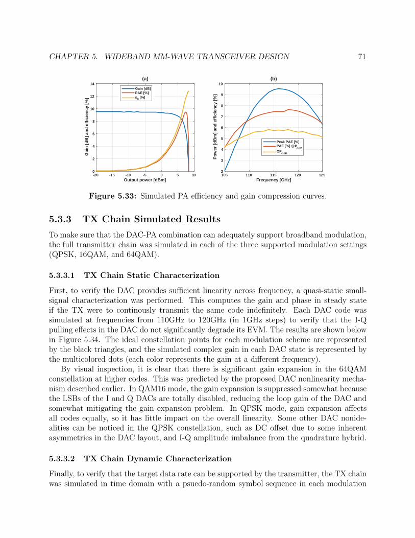
CHAPTER 5. WIDEBAND MM-WAVE TRANSCEIVER DESIGN 71
Output power [dBm]-20 -15 -10 -5 0 5 10
Gai
n [d
B] a
nd e
ffici
ency
[%]
0
2
4
6
8
10
12
14Gain [dB]PAE [%]
Frequency [GHz]105 110 115 120 125
Pow
er [d
Bm
] and
effi
cien
cy [%
]
2
3
4
5
6
7
8
9
10
Peak PAE [%]PAE [%] @ P-1dBOP-1dB
ηD [%]
(b)(a)
Figure 5.33: Simulated PA efficiency and gain compression curves.
5.3.3 TX Chain Simulated Results
To make sure that the DAC-PA combination can adequately support broadband modulation,the full transmitter chain was simulated in each of the three supported modulation settings(QPSK, 16QAM, and 64QAM).
5.3.3.1 TX Chain Static Characterization
First, to verify the DAC provides sufficient linearity across frequency, a quasi-static small-signal characterization was performed. This computes the gain and phase in steady stateif the TX were to continously transmit the same code indefinitely. Each DAC code wassimulated at frequencies from 110GHz to 120GHz (in 1GHz steps) to verify that the I-Qpulling effects in the DAC do not significantly degrade its EVM. The results are shown belowin Figure 5.34. The ideal constellation points for each modulation scheme are representedby the black triangles, and the simulated complex gain in each DAC state is represented bythe multicolored dots (each color represents the gain at a different frequency).
By visual inspection, it is clear that there is significant gain expansion in the 64QAMconstellation at higher codes. This was predicted by the proposed DAC nonlinearity mecha-nism described earlier. In QAM16 mode, the gain expansion is suppressed somewhat becausethe LSBs of the I and Q DACs are totally disabled, reducing the loop gain of the DAC andsomewhat mitigating the gain expansion problem. In QPSK mode, gain expansion affectsall codes equally, so it has little impact on the overall linearity. Some other DAC nonide-alities can be noticed in the QPSK constellation, such as DC offset due to some inherentasymmetries in the DAC layout, and I-Q amplitude imbalance from the quadrature hybrid.
5.3.3.2 TX Chain Dynamic Characterization
Finally, to verify that the target data rate can be supported by the transmitter, the TX chainwas simulated in time domain with a psuedo-random symbol sequence in each modulation

CHAPTER 5. WIDEBAND MM-WAVE TRANSCEIVER DESIGN 72
Figure 5.34: Static TX constellations from 110GHz to 120GHz
setting.Simulations predict that 50Gb/s data rate should be achievable using either QPSK or
16QAM modulation. In QPSK mode, there is a fair amount of inter-symbol interference(ISI) coming from the transmitter itself (Figure 5.35) which suggests that this cannot bepushed much faster. However, in 16QAM mode, due to the lower symbol rate, the ISI isreduced (Figure 5.36). This represents the potential to improve the data rate of the linkfurther, if the SNR at the receiver is sufficiently high.

CHAPTER 5. WIDEBAND MM-WAVE TRANSCEIVER DESIGN 73
fRF=110GHz fRF=112GHz fRF=114GHz fRF=116GHz fRF=118GHz fRF=120GHz1.5
10.5
0-0.5
-1-1.5
0 20 40
0-1 1
1.51
0.50
-0.5-1
-1.5
1.51
0.50
-0.5-1
-1.50 20 40
0-1 1
1.51
0.50
-0.5-1
-1.5
1.51
0.50
-0.5-1
-1.50 20 40
0-1 1
1.51
0.50
-0.5-1
-1.5
1.51
0.50
-0.5-1
-1.50 20 40
0-1 1
1.51
0.50
-0.5-1
-1.5
1.51
0.50
-0.5-1
-1.50 20 40
0-1 1
1.51
0.50
-0.5-1
-1.5
1.51
0.50
-0.5-1
-1.50 20 40
0-1 1
1.51
0.50
-0.5-1
-1.5
EVM=20.0%(-14.0dB) EVM=18.8% (-14.5dB) EVM=18.1% (-14.9dB) EVM=18.1% (-14.9dB) EVM=17.8% (-15.0dB) EVM=18.6% (-14.6dB)
Figure 5.35: Simulated QPSK eye diagram and constellations for 40ps symbol period,corresponding to 50Gb/s data rate
fRF=110GHz
1
0
-1
0 40 80
0-1 1
1
0
-1
EVM=6.9%(-23.2dB)
fRF=110GHz
1
0
-1
0-1 1
1
0
-1
EVM=6.9%(-23.2dB)
fRF=112GHz
1
0
-1
0 40 80
0-1 1
1
0
-1
EVM=6.4%(-23.9dB)
1
0
-1
0-1 1
1
0
-1
fRF=114GHz
1
0
-1
0 40 80
0-1 1
1
0
-1
EVM=5.9%(-24.6dB)
1
0
-1
0-1 1
1
0
-1
fRF=116GHz
1
0
-1
0 40 80
0-1 1
1
0
-1
EVM=5.4%(-25.4dB)
1
0
-1
0-1 1
1
0
-1
fRF=118GHz
1
0
-1
0 40 80
0-1 1
1
0
-1
EVM=5.0%(-26.0dB)
1
0
-1
0-1 1
1
0
-1
fRF=120GHz
1
0
-1
0 40 80
0-1 1
1
0
-1
EVM=5.1%(-25.9dB)
1
0
-1
0-1 1
1
0
-1
Figure 5.36: Simulated 16QAM eye diagram and constellations for 80ps symbol period,corresponding to 50Gb/s data rate
fRF=110GHz
60
1
0
-1
0-1 1
1
0
-1
EVM=7.8%(-22.1dB)
0 120
fRF=112GHz
60
1
0
-1
0-1 1
1
0
-1
EVM=11.2%(-19.0dB)
0 120
fRF=114GHz
60
1
0
-1
0-1 1
1
0
-1
EVM=11.1%(-19.1dB)
0 120
fRF=116GHz
60
1
0
-1
0-1 1
1
0
-1
EVM=6.2%(-24.1dB)
0 120
fRF=118GHz
60
1
0
-1
0-1 1
1
0
-1
EVM=10.4%(-19.7dB)
0 120
fRF=120GHz
60
1
0
-1
0-1 1
1
0
-1
EVM=9.6%(-20.3dB)
0 120
Figure 5.37: Simulated 64QAM eye diagram and constellations for 120ps symbol period,corresponding to 50Gb/s data rate

CHAPTER 5. WIDEBAND MM-WAVE TRANSCEIVER DESIGN 74
5.4 Receiver
5.4.1 Baseband Amplification
The baseband amplification chain and output driver were designed by Sashank Krishna-murthy, and are briefly summarized here. The main amplifier chain is designed around aninverter-based Cherry-Hooper amplifier core [78]. This allows maximizing both gain andbandwidth, rather than the usual gain-bandwidth tradeoff of a single-stage amplifier. Be-cause the inverter-based amplifier does not have any inherent common-mode rejection, aunity-gain differential buffer amplifier has been inserted before each Cherry-Hooper stage toprovide additional common-mode rejection. Series DC-blocking capacitors are used to de-couple common-mode voltages between stages and reduce the impact of DC offset voltagesin each amplifier stage.
CESD
CESD
chip to PCBtransition
Cherry-HooperGain Stages
Common-ModeRejection Buffers
Output driver
R=50Ω
ℓ=190μm,Z0=100Ω
R=50Ω
ℓ=615μm, Z0=100Ω
Figure 5.38: Baseband amplifiers and output driver
Following the Cherry-Hooper stages, a PMOS output driver is used to drive the differ-ential signal off chip. A PMOS output driver was selected so that the output signal fromthe chip will be truly ground referenced, rather than referenced to ground through an on-chip bypass capacitor (as in the NMOS case). A shunt peaking inductor is placed alongthe transmission line to extend the bandwidth of the chain. ESD protection at the outputis provided using a series inductor with a capacitor at the center tap. This behaves as anartificial transmission line and absorbs the impact of the ESD capacitance without impactingthe bandwidth too much.
The simulated performance of the baseband amplification chain predicts an in-band gainof 24.7dB, with a 3dB bandwidth of 13.5GHz. Because of additional losses induced by theskin effect in the peaking inductor and transmission line routing, the gain drops slightly from24.7dB to 24.5dB from 100MHz and 5GHz. The DC blocking capacitors in between stagesresult in a low-frequency 3dB cutoff of 7.6MHz.

CHAPTER 5. WIDEBAND MM-WAVE TRANSCEIVER DESIGN 75
Frequency1MHz
Gai
n [d
B]
0
5
10
15
20
25
30
10MHz 100MHz 1GHz 10GHz 100GHz
24.7dB 24.5dB
Figure 5.39: Voltage gain of baseband amplifier and output driver (including transmissionline routing)
5.4.2 Active Mixer with TIA load
It has been demonstrated that as the carrier frequency approaches the fmax of the technology,a passive mixer can provide better noise performance than an active mixer [79]. Additionally,because the passive mixer input impedance is an upconverted version of its baseband loadimpedance, it is also straightforward to provide a wideband input impedance for the mixer.However, in 28nm at 120GHz, the operation frequency is still only about half of fmax, sothere may still be some benefit in using an active mixer instead of a passive mixer.
For a fair comparison between active and passive mixers, the transconductor device typ-ically present in an active Gilbert-cell mixer is omitted here. Instead, the RF signal can betransformer coupled into the sources of the Gilbert-cell. This can easily be done for bothpassive and active mixers.
If the mixer operation is viewed as purely current-commutating, there is no significantdifference in conversion gain between a passive and active mixer [80]. All of the RF currentis commutated to baseband and flows through the baseband load. Therefore, the tran-simpedance gain of the mixer is set only by the baseband load resistance, regardless ofwhether it is an active or passive mixer. However, this assumes the input signal is a truecurrent source, with infinite source impedance.
If the source impedance is finite, then there is a current divider between the sourceimpedance and mixer input impedance. There is also effectively a “current commutationgain” which represents the fraction of current that gets downconverted to baseband, depen-

CHAPTER 5. WIDEBAND MM-WAVE TRANSCEIVER DESIGN 76
Mixer IF port
Mixer RF port
Mixer LO port
Figure 5.40: Double balanced active mixer core schematic
dent on the swing on the LO port. So, the transimpedance gain is determined by the productof these two factors, multiplied by the baseband load impedance (Equation 5.42).
ZT =Zout(LNA)
Zin(mixer) + Zout(LNA)
·GI · ZL,BB (5.42)
Unlike in a passive mixer, an active mixer’s input impedance has little dependence on itsload impedance. So, it is possible to reduce the input impedance without changing the loadimpedance, leading to a higher overall effective transimpedance gain.
One final drawback of a passive mixer is that its conversion gain is more sensitive to theLO swing. For an efficiency-optimized high frequency design, it is advantageous to use anactive mixer instead to save power on the mixer LO driver.
Typically, a current-commutating mixer assumes a hard-switching LO waveform - usuallya large-amplitude square wave with fast rise and fall times. However, the mixer LO waveformat millimeter-wave will be unlikely to be a square wave. A noise and gain analysis byTerrovitis assumes square wave LO drive, with some approximations for large sinusoidalLO signals [81]. For moderate or low LO signal levels, these approximations do not yieldaccurate predictions.
Another paper by Melly et al provides more detailed modeling of sinusoidally drivenmixers [82]. Conversion gain can be analytically computed in the subthreshold (weak in-version) and strong inversion modes of operation (Equations 5.4.2). The analysis becomestoo difficult for operation in moderate inversion or operation that crosses the boundaries of

CHAPTER 5. WIDEBAND MM-WAVE TRANSCEIVER DESIGN 77
these regions of operation. For large LO swing in any region of operation, the conversion
gain is simply2
π.
GI =VLO
2nkTq
(Weak inversion, low LO swing) (5.43a)
GI =VLO
4nkTq
√2ISItail
(Strong inversion, low LO swing) (5.43b)
GI =2
π(High LO swing) (5.43c)
There are a few caveats to the equations above [82]:
1. Quasistatic devices are assumed, and therefore the equations may not necessarily agreewith simulations at higher frequencies.
2. Truly differential pairs are assumed, rather than the pseudodifferential pairs of Figure5.40.
The “typical” CMOS Gilbert-cell mixer design has been analyzed in detail for bothconversion gain and noise figure. However, this design is not quite typical in that this Gilbert-cell mixer does not use a tail device to set the bias point, nor does it use transconductordevices to provide current gain. To save supply headroom, instead the sources of the mixerdevices are all DC-connected to ground. The RF signal can be magnetically coupled intothe sources using a transformer.
Because of this choice of topology, with large-signal LO drive, the DC current of themixer will shift away from the quiescent bias point. Under these large signal conditions, theconventional mixer analysis of equation is not strictly valid, but it serves as a good designapproximation.
RP RP
(a) (b) (c)
Cin,BB Cin,BB
Cin,BB
RF
RF
Figure 5.41: Different strategies for the DC load of the mixer: Resistor load (a), PMOSload (b), PMOS load with TIA (c).

CHAPTER 5. WIDEBAND MM-WAVE TRANSCEIVER DESIGN 78
The output of the mixer needs to be DC-connected to either a resistive (Figure 5.41a) oractive (Figure 5.41b) load. According to Equation 5.42, the mixer load impedance should bemaximized to maximize its transimpedance gain. With a fixed load capacitance (set by theinput capacitance of the baseband amplification), this then determines the gain-bandwidthtradeoff of the mixer. However, if large bandwidth is desired, there is not a significant differ-ence in the range of possibilites between active and resistive loads (Figure 5.42a). So, giventhat the output of the mixer goes directly to the pseudo-differential baseband amplificationstage, the active load is preferred since it can easily be adjusted to set the output commonmode to the desired level.
6 8 10 12 14 16 18 20BW [GHz]
10
15
20
25
30
35
40
conv
. gai
n [d
B]
2.4μm PMOS4μm PMOS4.8μm PMOS7.2μm PMOSResistive load
6 8 10 12 14 16 18 20BW [GHz]
10
15
20
25
30
35
40
conv
. gai
n [d
B]
2.4μm PMOS4μm PMOS4.8μm PMOS7.2μm PMOSResistive load2.4μm PMOS (TIA)4μm PMOS (TIA)4.8μm PMOS (TIA)9.6μm PMOS (TIA)
(a) (b)Figure 5.42: Range of gain and bandwidth possibilites for different mixer baseband loads.
However, there is another option that can break the gain-bandwidth tradeoff. An in-termediate gain stage, in the form of a transimpedance amplifier, can provide a low inputimpedance to the mixer output, while also driving the input capacitance of the basebandamplifier with high bandwidth. By varying the feedback resistance RF in the inverter-basedTIA, a curve of possible values of gain and bandwidth can be traced out (Figure 5.42b). Fora desired mixer bandwidth of 18GHz or more, the feedback resistance is low and the addedloading of the TIA becomes harmful rather than helpful. However, for a mixer bandwidth of14-17GHz, the TIA is helpful in providing higher gain for the same bandwidth. Similarly, fora given gain requirement, the bandwidth in the TIA-based mixer is strictly higher. The onlypenalty is DC power, which (for a small size inverter) is not a significant increase overall.
Unfortunately, due to layout-related complications, some more effort is required to acheivethis performance. To support broad bandwidth at the baseband output, the output padsthemselves need to be on the perimeter of the die, so they can be easily and cleanly routed

CHAPTER 5. WIDEBAND MM-WAVE TRANSCEIVER DESIGN 79
away from the chip on the PCB. With a limited number of IO bumps available, this meantthat the I and Q output pads for a single channel needed to be on the same side of the chip.To make this happen, the I signal (at either LO, RF, or baseband) needed to cross underneaththe Q signal. The least painful and most symmetric way to do this is at baseband, thoughit still requires some care in layout.
The layout floorplan for the mixer (Figure 5.44) illustrates the dilemma. The basebandoutput signal from the “Q” mixer is routed underneath the “I” LO input. For matchingof performance between I and Q, the I mixer is routed in a similar way, with a matchedpath length. Effectively, this adds an RC routing line at the output of the mixer (Figure5.43), which has a gain and bandwidth impact. This can be overcome somewhat by adding asecond TIA at the end of the RC routing, to absorb some of the routing capacitance with alower impedance termination and drive the baseband amplifier input with a high bandwidth.
(to baseband amp)
RX routing RC model
RX mixing core
Mixer active load
Mixer RF port
Mixer LO port
Figure 5.43: Finalized mixer schematic.

CHAPTER 5. WIDEBAND MM-WAVE TRANSCEIVER DESIGN 80
Basebandamp (I)
Basebandamp (Q)
LO(I)
LO(Q)
RF(I)RF(Q)
Figure 5.44: Mixer layout floorplan. Due to IO pad constraints, the I and Q baseband ampsboth need to be on the same side of the mixers, necessitating routing the mixer basebandoutputs a long distance (shown in thin cyan lines).

CHAPTER 5. WIDEBAND MM-WAVE TRANSCEIVER DESIGN 81
5.4.3 LNA
The LNA design is based around a common-source neutralized differential amplifier, usingthe same layout neutralization style as in the power amplifier. The extremely broad-bandinput match (Figure 5.46 is provided mostly by the loss of the input transformer and thechip-to-PCB transition (the chip-to-PCB model is included in all receiver simulations).
After the first LNA stage, the signal is split into two separate amplification paths. Thisis to isolate the I and Q mixers from each other and prevent the possibility of any LO ornoise coupling between them. The total LNA gain to a single output, including the 3dB lossfrom the split, is simulated to be 8dB at the center frequency of 115GHz (Figure 5.47). TheLNA has a 3dB bandwidth of 31GHz, but this comes at the cost of increased group delayripple of 30ps.
The simulated LNA noise figure is less than 9dB over the full 100-130GHz band (Figure5.48). The noise figure peaks significantly towards the higher end of this band. This is aconsequence of increasing packaging losses above 130GHz.
5.5fF
5.5fF119Ω
119Ω
chip to PCBtransition
Figure 5.45: LNA schematic

CHAPTER 5. WIDEBAND MM-WAVE TRANSCEIVER DESIGN 82
20 50 100
200
500
+j20
-j20
+j50
-j50
+j100
-j100
+j200
-j200
+j500
-j500
0.0 ∞
Frequency [GHz]90 100 110 120 130 140
S11
[dB
]
-30
-25
-20
-15
-10
-5
0
31 GHz
100.5 GHz 131.5 GHz
Figure 5.46: Simulated LNA input impedance seen from PCB (including chip-to-PCBtransition model)
Frequency [GHz]90 100 110 120 130 140
LNA
Gai
n [d
B]
-6
-4
-2
0
2
4
6
8
90 100 110 120 130 140
Gro
up D
elay
[ps]
180
190
200
210
220
230
240
250
260
Frequency [GHz]
31 GHz
99.5 GHz 130.5 GHz
Figure 5.47: Simulated LNA Gain and Group Delay (including 3dB loss from I-Q split)

CHAPTER 5. WIDEBAND MM-WAVE TRANSCEIVER DESIGN 83
Frequency [GHz]90 100 110 120 130 140
Noi
se F
igur
e [d
B]
6
7
8
9
10
11
12
13
14
15
Figure 5.48: Simulated LNA Noise Figure
5.4.4 RX Chain Simulated Performance
For verification of the complete system, the full receiver chain was simulated together usingan LO frequency of 115GHz. The transceiver has nearly 44dB of conversion gain (8dB LNA+ 11dB mixer + 25dB baseband), with a 3dB bandwidth of 10GHz (Figure 5.49).
The (double sideband) noise figure in-band for the complete chain is simulated to be11.2dB (Figure 5.50). Because of the AC coupling capacitance in the baseband, and thepresence of flicker noise, the noise figure increases dramatically below 25MHz.

CHAPTER 5. WIDEBAND MM-WAVE TRANSCEIVER DESIGN 84
Baseband output frequency100GHz
Volta
ge c
onve
rsio
n ga
in [d
B]
15
20
25
30
35
40
45
10GHz1GHz100MHz10MHz1MHz
43.8dB
40.8dB@10GHz
Figure 5.49: Simulated conversion gain of the full receiver chain, including LNA, mixer,and baseband amplification. The x-axis represents the frequency offset from the 115GHz LOsignal and the baseband tone frequency that it downconverts to.
Baseband output frequency10GHz 100GHz
Noi
se F
igur
e [d
B]
10
11
12
13
14
15
16
17
18
19
20
100MHz 1GHz1MHz 10MHz
11.2dB@2GHz
14.2dB@15GHz
14.2dB@22MHz
Figure 5.50: Simulated double sideband noise figure for the full RX chain with 115GHzLO frequency.
5.5 PCB and Antenna Design
The choice of PCB materials and stackup is influenced by several factors. The dielectricfor the top routing layer of the PCB should be thin to minimize surface wave excitationfrom the chip-PCB transition. For a symmetric board stackup, the dielectric for the bottom

CHAPTER 5. WIDEBAND MM-WAVE TRANSCEIVER DESIGN 85
routing layer should therefore also be thin — asymmetric stackups are possible but prone towarpage, creating issues for the assembly process.
To keep costs low, the board has only a four layer construction, with two routing layersand two plane layers. So, the only dimension left undetermined is the thickness of theinternal dielectric between the two plane layers. A thicker dielectric means a thicker PCBwhich is more rigid, and is simpler to assemble and more robust. But coupling into surfacewaves from the antenna is worsened with a thicker dielectric.
solder mask (0.5mil)
1oz Cu(1.4mil)
0.5oz Cu(0.7mil)
0.5oz Cu(0.7mil)
1oz Cu(1.4mil)
solder mask (0.5mil)
Megtron62mil
Megtron62mil
Megtron610mil
Figure 5.51: Selected PCB stackup.
Several classes of high-performance PCB materials are available, few of which have beencharacterized at millimeter-wave. Table 5.2 lists a variety of commercially available ma-terials, with loss tangents ranging over two orders of magnitude. The lowest loss material,CuFlon from PolyFlon, is a pure PTFE (Teflon) material, while nearly all other PTFE basedmaterials are reinforced with glass fibers or ceramic filled and have higher losses. The trade-off is that pure PTFE is very difficult to work with, with reinforced PTFE being somewhatsimpler. A standard off-the-shelf FR-4 material, Isola 370HR, is the highest loss, but sim-plest to assemble into a multilayer board. The Megtron line of materials offers a compromisebetween complexity of assembly (similar to FR-4) and high-frequency performance, so it wasselected for the final antenna design.
To interface smoothly with the differential I/O from the transceiver IC, it is desirable tohave a differential antenna as well. The antenna should have broadband operation (wide S11bandwidth, and flat gain vs frequency) while also having high polarization purity to enabledual-polarization data transmission with two antennas.
5.5.1 Folded Dipole Antenna
Initial design investigations showed that a folded dipole antenna on a thin substrate canprovide moderate S11 -10dB bandwidth of 12GHz (Figure 5.52a). Although this is not

CHAPTER 5. WIDEBAND MM-WAVE TRANSCEIVER DESIGN 86
Table 5.2: Characteristics of Various PCB Materials
PCB CoreMaterial
DielectricConstant
LossTangent @10GHz
Loss Tangent@120GHz(estimated)
MinimumThickness
Material Type
Rogers 5880 2.20 0.00090.0015 -0.0022[83]
5milGlass microfiberreinforced PTFE
RogersXT/duroid8000
3.23 0.0035 — 2mil Thermoplastic
RogersULTRALAM3850
3.14 0.0025 0.007 [84] 1milLiquid crystallinepolymer (LCP)
Nelco NY9208 2.08 0.0006 — 30milReinforcedPTFE laminate
Nelco NY9217 2.17 0.0008 — 5milReinforcedPTFE laminate
TaconicFastRise
2.74 0.0014 — 2milCeramic,thermoset andPTFE
Taconic TLP-3 2.33 0.0009 — 5milFiberglass fabriccoated withPTFE
Taconic TLX-9 2.5 0.0015 — 2milPTFE fiberglasslaminate
Megtron7R-5785(N)
3.20 0.002 0.008 2milPPE blend resinsystem
Megtron6R-5775(N)
3.22 0.004 0.011 2milPPE blend resinsystem
PolyflonCuFlon
2.05 0.00045* — 0.25mil Pure PTFE
Isola 370HR 3.63 0.03 — 2milFR-4 (Epoxyresin)
*Datasheet reports loss tangent at 18GHz
sufficient to operate at the maximum designed data rate, this antenna structure was a goodenough starting point to justify further investigation.
The antenna, depicted in Figure 5.52b, is designed using a single thin sheet (2mil) ofdielectric, with a differential microstrip transmission line feed referenced to a ground planeunderneath the dielectric. There is a ground plane cutout around the antenna region toallow the antenna to radiate properly. Without the cutout, image currents will form in theground plane that cancel out the currents in the antenna, which would significantly decreasethe radiated power.
However, it’s not possible to package the entire chip on such a thin substrate, since mul-tiple routing layers are required for all of the other non-RF I/O from the chip. A thicker,multilayer substrate presents additional challenges. The added dielectric material under-neath the antenna effectively increases the capacitance of the distributed structure, loweringits input impedance. It also impacts the front to back ratio of the antenna, as it becomesdifficult to prevent radiation out of the back side of the antenna. Most problematically, the

CHAPTER 5. WIDEBAND MM-WAVE TRANSCEIVER DESIGN 87
Frequency [GHz]100 105 110 115 120 125 130
S 11 [d
B]
-40
-35
-30
-25
-20
-15
-10
-5
0
12GHz
(a) Input impedance of folded dipole antenna (b) 3D model of folded dipole antenna
antenna couples its energy into surface waves much more easily on the thicker substrate.This can be seen by looking at the radiation pattern of the antenna at different frequencies(Figure 5.53).
The surface waves impact the radiation pattern by traveling through the substrate untilthey reach a discontinuity (a via, piece of metal, or the edge of the board). At the point ofdiscontinuity, the surface wave diffracts and couples some energy into free space [85]. Becausethe surface waves undergo a different phase shift at different frequencies, this effect appearsas a “ripple” superimposed on a plot of gain versus frequency. In Figure 5.53, this effectappears as smaller side lobes of the radiation pattern that change location with frequency.
Theta [degrees]-180 -90 0 90 180
Gai
n [d
Bi]
-16
-14
-12
-10
-8
-6
-4
-2
0
2
4
6
Theta [degrees]-180 -90 0 90 180
Gai
n [d
Bi]
-16
-14
-12
-10
-8
-6
-4
-2
0
2
4
6
100GHz105GHz110GHz115GHz
120GHz125GHz130GHz
100GHz105GHz110GHz115GHz
120GHz125GHz130GHz
Folded Dipole on Thin Substrate Folded Dipole on Thick Substrate
Figure 5.53: Simulated antenna radiation pattern (θ representing the polar angle from thez-axis) versus frequency for thick and thin substrates

CHAPTER 5. WIDEBAND MM-WAVE TRANSCEIVER DESIGN 88
5.5.2 Surface Waves
In general, a surface wave is defined as a wave that propagates at the interface of twodielectrics [75]. The fields in a surface wave drop off exponentially when moving awayfrom the interface surface [86]. Surface waves can propagate with various configurations ofdielectrics and conductors, but the most relevant surface wave configuration for this PCBstructure is the grounded dielectric sheet (Figure 5.55). This structure supports both TMand TE modes, and interestingly (but problematically) the lowest order TM mode has acutoff frequency of zero (Eq. 5.44) [75].
fc,TM =nc
2d√ε− 1
, n = 0, 1, 2, ... (5.44a)
fc,TE =(2n− 1) c
4d√ε− 1
, n = 1, 2, 3, ... (5.44b)
For a dielectric with a relative permittivity of 3.2, and a thickness of 12mil, the cutofffrequency for the first TE mode is 166GHz. So, the only surface wave mode of concern isthe TM0 mode.
0.5oz Cu(0.7mil)
1oz Cu(1.4mil)
solder mask (0.5mil)
Megtron62mil
Megtron62mil
Megtron610mil
Figure 5.54: Dielectric slab which supports TM0 surface waves.
Figure 5.55: Calculated H field of grounded slab TM0 surface wave mode according totheory. The horizontal axis is the direction of propagation, and the vertical distance fromthe bottom of the image. The white horizontal line represents the air-dielectric interface.

CHAPTER 5. WIDEBAND MM-WAVE TRANSCEIVER DESIGN 89
5.5.3 Methods for Dealing with Surface Waves
Because of the difficult-to-predict and problematic impact of surface waves on the radiationpattern of the antenna, several methods have been proposed to mitigate those issues.
Figure 5.56: Sievenpiper “mushroom” EBG structure, side view.
Sievenpiper et al. proposed an artificial surface made of sub-wavelength structures thatprevents surface wave propagation within a forbidden band [85]. This structure, also knownas an “artifical magnetic conductor”, behaves similarly to a theoretical magnetic conductorover the band of operation. The exact structure proposed uses conductive patches on thetop metal layer of a PCB, connected to the ground plane through a central via (Figure 5.56),and is referred to as a “mushroom” or “Sievenpiper” EBG (electromagnetic band gap) in theliterature. Resonance between the inductance of the vias/ground plane and the capacitancebetween the patches results in the desired EBG behavior around the resonant frequency [87].
There are few examples in the literature of this type of EBG structure at mm-Wave;only a handful of 60GHz designs have made use of the technique [88][89]. For operationabove 100GHz, the large electrical size of the available vias in this PCB technology (bothdiameter and height) makes it prohibitive to use this approach. Artificial magnetic conductortechinques have been demonstrated that do not use vias [90] for the purpose of replacinga back reflector ground plane in an antenna. However, it is not clear if these types ofconstructions can also be used to suppress surface wave propagation.
Another approach is to try to capture and re-radiate whatever surface waves are launchedby the antenna structure [91]. This has the added benefit of increasing the gain of theantenna because of the larger effective aperture that is contributing to free-space radiation.A potential drawback is that, due to the nonzero propagation delay of the surface wave fromthe main antenna to the re-radiation structure, the two radiated signals will only be in phaseat one frequency. Away from that frequency, the gain will drop off as the two waves start tointerfere destructively.
Based on the design from University of Nice[91], an aperture coupled patch antenna witha grounded-via guard ring was designed using the PCB stackup in Figure 5.51. By looking atthe radiation pattern as the substrate size is swept, the effectiveness of the ring in capturingsurface waves is clear (Figure 5.57). In contrast, the radiation pattern of the antenna withoutthe guard ring is very unstable as the substrate size is varied, indicating a large amount ofenergy coupled into surface waves.

CHAPTER 5. WIDEBAND MM-WAVE TRANSCEIVER DESIGN 90
To capture even more surface waves, a second via ring can be added, although this doesnot provide a significant increase in antenna gain. It does create a radiation pattern that isvery stable versus PCB size, so there is little energy that propagates outside the structureas surface waves (Figure 5.57). The downside is a more narrow-band radiation pattern.Because the distance to the second ring is further, this added time delay means the phaseof its radiated field, relative to that of the main patch, will change more quickly versusfrequency. This also leads to greater and steeper group delay variation versus frequency(Figure 5.59).
Another potential solution to the surface wave problem is to surround the antenna witha trench. This will prevent surface waves from propagating, since there is no media forthe wave to travel through any more (in practice, some nonzero amount of energy will stillcouple across the gap). A thorough investigation based on a design at 2.4GHz has shown thatbroadside gain can be enhanced by up to 2.7dB by removing the substrate around the patch[92]. The substrate is removed right up to the edge of the patch, so the fringing fields extendout of the substrate material into the air. Partial and complete removal is investigated in
Angle from broadside-180° -90° 90° 180°
Gai
n [d
Bi]
-10
-5
0
5
10
Patch with ground ring
Gai
n [d
Bi]
-10
-5
0
5
10
Patch without ground ring
0°Angle from broadside
-180° -90° 90° 180°0°
Figure 5.57: Patch antenna gain (at 115GHz) with and without guard ring, as the PCBsubstrate size is varied.
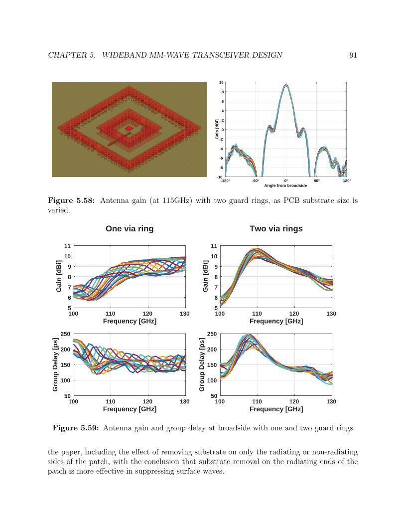
CHAPTER 5. WIDEBAND MM-WAVE TRANSCEIVER DESIGN 91
Angle from broadside-180° -90° 90° 180°
Gai
n [d
Bi]
-10
-8
-6
-4
-2
0
2
4
6
8
10
0°
Figure 5.58: Antenna gain (at 115GHz) with two guard rings, as PCB substrate size isvaried.
Frequency [GHz]100 110 120 130
Gai
n [d
Bi]
56789
1011
Frequency [GHz]100 110 120 130
Gro
up D
elay
[ps]
50
100
150
200
250
Two via rings
Frequency [GHz]100 110 120 130
Gai
n [d
Bi]
56789
1011
Frequency [GHz]100 110 120 130
Gro
up D
elay
[ps]
50
100
150
200
250
One via ring
Figure 5.59: Antenna gain and group delay at broadside with one and two guard rings
the paper, including the effect of removing substrate on only the radiating or non-radiatingsides of the patch, with the conclusion that substrate removal on the radiating ends of thepatch is more effective in suppressing surface waves.

CHAPTER 5. WIDEBAND MM-WAVE TRANSCEIVER DESIGN 92
Similar techniques have been tried at 60GHz [93], and a 2.3-2.8dB increase in gain isreported for the removed-substrate antennas. A downside is that this effect also appears tocorrespond with a reduction in impedance bandwidth, hypothesized by the authors of thatpublication to be because of higher field concentration near the edge of the removed regionthat increases the Q of the antenna resonance.
Because of this bandwidth reduction effect, and concerns about the sensitivity of antennainput impedance to the tolerances of the substrate removal process, the substrate removalstrategy used here was somewhat different than that has been shown in the literature. In-stead, the grounded via ring described earlier is included in the design, and the substrate isonly removed in the area outside of the ring (Figure 5.60), forming a “trench” around thering. This ensures that any surface waves that are not captured by the ring are re-radiatedin a controlled way, and do not travel further away from the antenna. Simulations showthat there is little impact on the antenna input impedance from PCB features outside thering, so surface waves can be suppressed effectively by the cavity without any unpredictableimpacts on the input impedance.
h
feeddir.
Figure 5.60: Patch with grounded via ring and partial substrate removal
Simulated results predict that a trench surrounding a patch with a single via ring (designB) is fairly effective at suppressing surface waves (Figure 5.62). The simulations capture theeffect of surface waves by proxy: the substrate dimensions of the PCB material are variedand the variation in antenna gain at broadside is recorded. Notably, the “trench all around”(B) and “trench only on radiating sides” (E) have nearly identical surface wave suppression,while having the trench only on the non-radiating sides (D) is the same or worse than notrench at all (A). These results are consistent with what has been reported in the literature[92]. None of these solutions are as effective at suppressing surface waves as having two

CHAPTER 5. WIDEBAND MM-WAVE TRANSCEIVER DESIGN 93
via rings, but they do not have the negative side effect of significantly narrowed 3dB gainbandwidth.
A B C
D EFigure 5.61: Different surface wave suppression technques. Trench/substrate removal areasare shown in yellow.
Unfortunately, due to the fabrication constraints of the PCB vendor, it was not possibleto have the trench fully surround the antenna. The solution to this issue was to keep theantenna region supported on the left and right (along the direction of the feedline), sothe feedline is mechanically well-supported during the PCB multilayer lamination process.Unfortunately, this also implies that the substrate cannot be removed along the radiatingedges of the patch, leading to reduced overall surface wave suppression. To form a completetrench, the last bit of substrate material would need to be removed by an external vendorafter the multilayer PCB has been pressed together and vias added (the vias would benecessary to mechanically support the patch region after complete trenching). A photo ofthe final antenna design, with partial substrate removal, is shown in Figure 5.63.
The final simulated input impedance is plotted below in Figure 5.64, and has minimaldependence on the size of the substrate (i.e., is not impacted by surface waves).

CHAPTER 5. WIDEBAND MM-WAVE TRANSCEIVER DESIGN 94
Frequency [GHz]100 105 110 115 120 125 130
Gai
n va
riatio
n [d
B]
0
0.5
1
1.5
2
2.5
3
3.5A: One via ring, no trenchB: One via ring, trench all aroundC: Two via rings, no trenchD: One via ring, trench only on non-radiating sidesE: One via ring, trench only on radiating sides
Figure 5.62: Worst-case gain variation (minimum to maximum) of various surface wavemitigation techniques, as the (square) substrate size is varied from 12 to 15mm.
5.5.4 Planar Balun on PCB
Because the patch antenna is single-ended, but the chip has a fully differential interface, abalun is required to interface between the two. A planar microwave solution to this problemis the so-called “rat-race” hyrbid [75] (Figure 5.65a).
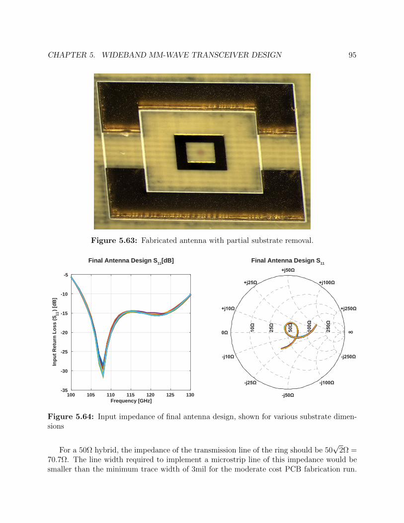
CHAPTER 5. WIDEBAND MM-WAVE TRANSCEIVER DESIGN 95
Figure 5.63: Fabricated antenna with partial substrate removal.
Frequency [GHz]100 105 110 115 120 125 130
Inpu
t Ret
urn
Loss
(S11
) [dB
]
-35
-30
-25
-20
-15
-10
-5
Final Antenna Design S11[dB]10Ω
25Ω
100Ω
250Ω
+j10Ω
-j10Ω
+j25Ω
-j25Ω
+j50Ω
-j50Ω
+j100Ω
-j100Ω
+j250Ω
-j250Ω
0Ω ∞
Final Antenna Design S11
50Ω
Figure 5.64: Input impedance of final antenna design, shown for various substrate dimen-sions
For a 50Ω hybrid, the impedance of the transmission line of the ring should be 50√
2Ω =70.7Ω. The line width required to implement a microstrip line of this impedance would besmaller than the minimum trace width of 3mil for the moderate cost PCB fabrication run.

CHAPTER 5. WIDEBAND MM-WAVE TRANSCEIVER DESIGN 96
Z0
√2
3⁄4λ
Z0
√2
1⁄4λ
Z0
√2
1⁄4λ
Z0
√2
1⁄4λ
Z0
Z0
Z0
Z0
Z0
3⁄4λ
Z0
1⁄4λ
Z0
1⁄4λ
Z0
1⁄4λ
Z0
1⁄4λ⁄√24
∆ port
Σ port
(c)(b)(a)∆ port
Z0 Z0 -port
+port
Figure 5.65: Design process for optimized rat-race hybrid without sum port termination.
Smaller line widths can be fabricated, but at significantly higher cost. To avoid this problem,a 35Ω hybrid is designed using a 35Ω impedance for the ring, and a series quarter wavelengthline is used to match back to 50Ω (Figure 5.65b).
This requires a matched termination on all ports to provide ideal isolation and common-mode rejection. However, it is extremely difficult to create an ideal 50Ω termination at120GHz on a PCB (even an ideal resistor would require a via to the ground plane underneath,contributing significant inductance). It has been shown that the termination on the “sum”port can be omitted at the cost of reducing the isolation of the balun [94] (Figure 5.65a).
The final balun design is shown in Figure 5.66a. The two differential ports are taperedwith a smooth bend to interface with a differential microstrip transmission line. Simulationspredict a loss of between 0.83 to 0.7 dB and 7ps variation in group delay over the 100 to130GHz band (Figure 5.66b). Simulated return losses for the differential and single endedports are below -15dB from 101 to 130GHz (Figure 5.66c). Common-mode conversion isworst at the low end of the frequency range, but still better than -15dB (Figure 5.66d).Since the common-mode impedance of the chip is not specifically designed to be matched,the common-mode performance will likely vary from this result in practice.

CHAPTER 5. WIDEBAND MM-WAVE TRANSCEIVER DESIGN 97
to antenna
to chip
(a) Final PCB layout of balun
Frequency [GHz]100 105 110 115 120 125 130
Loss
[dB]
-0.9
-0.8
-0.7
-0.6Balun Loss
Frequency [GHz]100 105 110 115 120 125 130
Gro
up D
elay
[ps]
115
120
125
130Balun Group Delay
(b) Simulated insertion loss and group delay
Frequency [GHz]100 105 110 115 120 125 130
Retu
rn L
oss
[dB
]
-20
-19
-18
-17
-16
-15
-14Balun Return Loss
Single-ended portDierential port
(c) Simulated return loss
Frequency [GHz]100 105 110 115 120 125 130
Gai
n [d
B]
-35
-30
-25
-20
-15
-10
-5
0Dierential vs common mode conversion gain
SE to dierential mode gainSE to common mode gain
(d) Simulated CM and DM conversion
Figure 5.66: Final balun design and simulations
Figure 5.67: Fabricated rat-race hybrid on PCB.
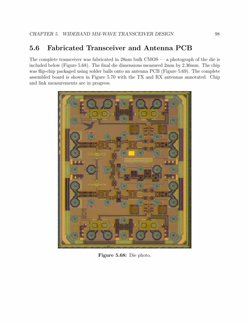
CHAPTER 5. WIDEBAND MM-WAVE TRANSCEIVER DESIGN 98
5.6 Fabricated Transceiver and Antenna PCB
The complete transceiver was fabricated in 28nm bulk CMOS — a photograph of the die isincluded below (Figure 5.68). The final die dimensions measured 2mm by 2.36mm. The chipwas flip-chip packaged using solder balls onto an antenna PCB (Figure 5.69). The completeassembled board is shown in Figure 5.70 with the TX and RX antennas annotated. Chipand link measurements are in progress.
Figure 5.68: Die photo.

CHAPTER 5. WIDEBAND MM-WAVE TRANSCEIVER DESIGN 99
Figure 5.69: Flip-chip footprint, differential routing, and mm-Wave baluns as fabricatedon PCB.

CHAPTER 5. WIDEBAND MM-WAVE TRANSCEIVER DESIGN 100
RX patches
TX patches
Figure 5.70: Antenna PCB with chip attached.

CHAPTER 5. WIDEBAND MM-WAVE TRANSCEIVER DESIGN 101
5.7 Performance Comparison
Table 5.3: Performance and Energy Efficiency of mm-Wave Wideband Transmitters
ReferenceCarrierFrequency[GHz]
Data Rate[Gb/s]
ModulationTechnique
DCpower[mW]
Energyefficiency[pJ/bit]
This work 115 2x50***QPSK, 16QAM,64QAM
2x110 +130(LO)***
2.7***(including LO)
Dolatsha, ISSCC 2017[54]
130 12.5† OOK 59 4.72
Yu, T-MTT 2014 [52] 60 16 OOK 19.2 1.2
Yang, RFIC 2014 [58] 155 20† QPSK 345‡ 17.25‡Jiang, JSSC 2017 [60] 220 2x12.2,2x40***ASK 2x450 36.9
Tokgoz, ISSCC 2018[62]
70,1052x60*,2x36**
64QAM,16QAM, QPSK,8-PSK
120 1*, 1.7**
†Complete link demonstrated‡Power for TX+RX*With equalization**Without equalization***Simulated
Table 5.4: Performance and Energy Efficiency of mm-Wave Wideband Receivers
ReferenceCarrierFrequency[GHz]
Data Rate[Gb/s]
ModulationTechnique
DCpower[mW]
Energyefficiency[pJ/bit]
This work 115 2x50***QPSK, 16QAM,64QAM
2x83 +130(LO)***
2.97***(including LO)
Dolatsha, ISSCC 2017[54]
130 12.5† OOK 38 3.04
Yu, TCAS-I 2015 [53] 60 18.7 OOK 11.6 0.62
Yang, RFIC 2014 [58] 155 20† QPSK 345‡ 17.25‡
Tokgoz, ISSCC 2018[62]
70,1052x60*,2x36**
64QAM,16QAM, QPSK,8-PSK
160 1.3*, 2.22**
†Complete link demonstrated‡Power for TX+RX*With equalization**Without equalization***Simulated

102
Chapter 6
Conclusion
6.1 Summary of Thesis
In this thesis, the designs for two highly-integrated broadband mm-Wave transceivers havebeen presented. Both transceivers have been integrated with antennas to facilitate system-level demonstrations.
First, circuit design techniques for a 94GHz phased-array FMCW radar system are ex-plored. Energy efficiency is optimized by system-level optimizations, and relaxation of indi-vidual element specifications due to phased array antenna gains. By careful design of sharedLO generation and distribution circuitry, the overhead power of these components can bekept under control to achieve an efficient system implementation.
The assembled chip and antenna module were then used to demonstrate beamformingon the receiver and transmitter. Radar measurements show that basic range measurementfunctionality is possible with high distance resolution, corresponding to the high availablecircuit bandwidth.
After the presentation of the radar IC, circuit techniques focusing on extending thefractional bandwidth in millimeter-Wave amplifiers were analyzed and presented. A keycontribution here is the proposal of an energy-efficient RF DAC supporting direct digitalmodulation of the millimeter-Wave carrier. Mechanisms for DAC nonlinearity have beenanalyzed and used to optimize the DAC design. A complete transmitter chain was thendesigned around the DAC to support 50Gb/s data transmission using QPSK, 16QAM, and64QAM modulation schemes.
A broadband millimeter-wave downconversion receiver was also analyzed and designedusing the same circuit principles. A thorough analysis of the gain-bandwidth tradeoffs ina receiver mixer reveals that a transimpedance amplifier load can be used to extend thebandwidth of the mixer without sacrificing gain. The full receiver chain was designed tosupport 10GHz of single-sideband RF bandwidth to support the targeted link data rate.
Finally, the antenna and packaging challenges associated with the transceiver were inves-tigated, resulting in a new antenna design with a milled trench for surface wave suppression.

CHAPTER 6. CONCLUSION 103
A wideband planar balun was designed to interface between the differential chip IO andthe single-ended antenna port. The transceiver IC was packaged onto the antenna printedcircuit board and is actively being characterized.
In summary, a nearly complete high-speed dual-polarization wireless link was proposedand implemented, including transmitter, receiver, and antennas. Simulations predict datarate and energy efficiency competitive with state-of-the-art frequency interleaved transceivers,with higher output power to support a link budget compatible with printed planar antennas.
6.2 Future Work
There are several steps that need to be taken in order to make the wideband transceiver de-sign of this thesis into a functional standalone system. Although there is significant researchactivity in the area of wideband mm-Wave transceivers, there has been very little activityto date towards addressing some of these practical system issues.
6.2.1 Carrier Recovery
As it is, the receiver is fed a ∼30GHz LO signal from off-chip, which is frequency multipliedup to mm-Wave. In the lab, this LO signal can be shared between the transmitter andreceiver for initial testing purposes. However, for a true wireless link, the receiver should beable to reconstruct the carrier of the transmitted signal and lock its own LO to the correctcenter frequency. It should also be able to track the close-in phase noise of the receivedsignal, to minimize the SNR degradation from the local LO.
One possibility is a Costas-loop style carrier recovery [95]. Although strictly intendedfor QPSK or BPSK, it could potentially also be used for QAM modulation by discardingthe interior points of the square QAM constellation (subsampling) or by using a limitingamplifier on the baseband data to turn the QAM signal into a QPSK-like data stream. Itmay be challenging to achieve high tracking bandwidth without compromising stability, sosome innovation may be required here.
Another possibility is to use a packet-based transmission scheme with a known pilotsequence for phase synchronization. This requires more intensive signal processing and couldbecome challenging for extremely wideband systems if the pilot sequence is used for a fullchannel estimation. On the other hand, if the pilot sequence is simply used as an aid forclose-in carrier recovery, it can be transmitted at a significantly reduced data rate.
A key challenge in the design of a carrier recovery loop, regardless of the implementationtechnique, will be desiging a tunable oscillator with sufficiently low phase noise. Outside thebandwidth of the carrier recovery loop, the phase noise of the RX LO will add to, ratherthan cancel, the phase noise of the received signal.

CHAPTER 6. CONCLUSION 104
6.2.2 Equalization
Another obstacle towards implementing a standalone system is the equalization of finitechannel bandwidth and finite polarization isolation. In its most basic form, a polarizationequalizer would simply act as a “de-rotation”, by removing any polarization crossover be-tween channels due to imperfect alignment. This is straightforward to implement given thatthe antenna alignment introduces no frequency dependence.
In reality, the antenna itself will have some frequency-dependent cross polarization, whichwill reduce the SNR of the desired polarization signal. A mixed-signal discrete time equalizeris the most straightforward way to deal with this and has already been demonstrated at60GHz at lower data rates [96].

105
Bibliography
[1] C. E. Shannon, “Communication in the presence of noise,” vol. 37, no. 1, pp. 10–21,1949.
[2] S. Emami, R. F. Wiser, E. Ali, M. G. Forbes, M. Q. Gordon, X. Guan, S. Lo, P. T.McElwee, J. Parker, J. R. Tani, J. M. Gilbert, and C. H. Doan, “A 60GHz CMOSphased-array transceiver pair for multi-Gb/s wireless communications,” in 2011 IEEEInternational Solid-State Circuits Conference, 2011, pp. 164–166.
[3] M. Boers, B. Afshar, I. Vassiliou, S. Sarkar, S. T. Nicolson, E. Adabi, B. G. Perumana,T. Chalvatzis, S. Kavvadias, P. Sen, W. L. Chan, A. H. T. Yu, A. Parsa, M. Nariman,S. Yoon, A. G. Besoli, C. A. Kyriazidou, G. Zochios, J. A. Castaneda, T. Sowlati, M.Rofougaran, and A. Rofougaran, “A 16TX/16RX 60 GHz 802.11ad Chipset With Sin-gle Coaxial Interface and Polarization Diversity,” IEEE Journal of Solid-State Circuits,vol. 49, no. 12, pp. 3031–3045, 2014.
[4] S. Trotta, M. Wintermantel, J. Dixon, U. Moeller, R. Jammers, T. Hauck, A. Samulak,B. Dehlink, K. Shun-Meen, H. Li, A. Ghazinour, Y. Yin, S. Pacheco, R. Reuter, S.Majied, D. Moline, T. Aaron, V. P. Trivedi, D. J. Morgan, and J. John, “An RCPPackaged Transceiver Chipset for Automotive LRR and SRR Systems in SiGe BiCMOSTechnology,” IEEE Transactions on Microwave Theory and Techniques, vol. 60, no. 3,pp. 778–794, 2012.
[5] C. Wagner, J. Bock, M. Wojnowski, H. Jager, J. Platz, M. Treml, F. Dober, R. Lach-ner, J. Minichshofer, and L. Maurer, “A 77GHz automotive radar receiver in a waferlevel package,” in 2012 IEEE Radio Frequency Integrated Circuits Symposium, 2012,pp. 511–514.
[6] B. P. Ginsburg, K. Subburaj, S. Samala, K. Ramasubramanian, J. Singh, S. Bhatara, S.Murali, D. Breen, M. Moallem, K. Dandu, S. Jalan, N. Nayak, R. Sachdev, I. Pratha-pan, K. Bhatia, T. Davis, E. Seok, H. Parthasarathy, R. Chatterjee, V. Srinivasan,V. Giannini, A. Kumar, R. Kulak, S. Ram, P. Gupta, Z. Parkar, S. Bhardwaj, Y. C.Rakesh, K. A. Rajagopal, A. Shrimali, and V. Rentala, “A multimode 76-to-81GHz au-tomotive radar transceiver with autonomous monitoring,” in 2018 IEEE InternationalSolid - State Circuits Conference - (ISSCC), 2018, pp. 158–160.

BIBLIOGRAPHY 106
[7] G. Avenier, M. Diop, P. Chevalier, G. Troillard, N. Loubet, J. Bouvier, L. Depoyan,N. Derrier, M. Buczko, C. Leyris, S. Boret, S. Montusclat, A. Margain, S. Pruvost,S. T. Nicolson, K. H. K. Yau, N. Revil, D. Gloria, D. Dutartre, S. P. Voinigescu,and A. Chantre, “0.13 µm SiGe BiCMOS Technology Fully Dedicated to mm-WaveApplications,” IEEE Journal of Solid-State Circuits, vol. 44, no. 9, pp. 2312–2321,2009.
[8] P. Chevalier, G. Avenier, G. Ribes, A. Montagne, E. Canderle, D. Celi, N. Derrier,C. Deglise, C. Durand, T. Quemerais, M. Buczko, D. Gloria, O. Robin, S. Petitdidier,Y. Campidelli, F. Abbate, M. Gros-Jean, L. Berthier, J. D. Chapon, F. Leverd, C.Jenny, C. Richard, O. Gourhant, C. De-Buttet, R. Beneyton, P. Maury, S. Joblot, L.Favennec, M. Guillermet, P. Brun, K. Courouble, K. Haxaire, G. Imbert, E. Gourvest,J. Cossalter, O. Saxod, C. Tavernier, F. Foussadier, B. Ramadout, R. Bianchini, C.Julien, D. Ney, J. Rosa, S. Haendler, Y. Carminati, and B. Borot, “A 55 nm triplegate oxide 9 metal layers SiGe BiCMOS technology featuring 320 GHz fT / 370 GHzfMAX HBT and high-Q millimeter-wave passives,” in 2014 IEEE International ElectronDevices Meeting, 2014, pp. 3.9.1–3.9.3.
[9] Y. Zhao and J. R. Long, “A Wideband, Dual-Path, Millimeter-Wave Power AmplifierWith 20 dBm Output Power and PAE Above 15% in 130 nm SiGe-BiCMOS,” IEEEJournal of Solid-State Circuits, vol. 47, no. 9, pp. 1981–1997, 2012.
[10] K. Khalaf, V. Vidojkovic, K. Vaesen, M. Libois, G. Mangraviti, V. Szortyka, C. Li,B. Verbruggen, M. Ingels, A. Bourdoux, C. Soens, W. V. Thillo, J. R. Long, and P.Wambacq, “Digitally Modulated CMOS Polar Transmitters for Highly-Efficient mm-Wave Wireless Communication,” IEEE Journal of Solid-State Circuits, vol. 51, no. 7,pp. 1579–1592, 2016.
[11] J. Chen, L. Ye, D. Titz, F. Gianesello, R. Pilard, A. Cathelin, F. Ferrero, C. Luxey, andA. M. Niknejad, “A digitally modulated mm-Wave cartesian beamforming transmitterwith quadrature spatial combining,” in 2013 International Solid-State Circuits Conf.Dig. Tech. Papers (ISSCC), (San Francisco, CA, USA), Feb. 2013, pp. 232–233.
[12] S. Callender, S. Pellerano, and C. Hull, “A 73GHz PA for 5G phased arrays in 14nmFinFET CMOS,” in 2017 IEEE Radio Frequency Integrated Circuits Symposium (RFIC),2017, pp. 402–405.
[13] L. Iotti, A. Mazzanti, and F. Svelto, “Insights Into Phase-Noise Scaling in Switch-Coupled Multi-Core LC VCOs for E-Band Adaptive Modulation Links,” IEEE Journalof Solid-State Circuits, vol. 52, no. 7, pp. 1703–1718, 2017.
[14] S. Kang and A. M. Niknejad, “A 100ghz active-varactor vco and a bi-directionallyinjection-locked loop in 65nm cmos,” in 2013 IEEE Radio Frequency Integrated CircuitsSymposium (RFIC), 2013, pp. 231–234.
[15] I. S. Merrill et al., “Introduction to Radar Systems,” Mc Graw-Hill, 2001.
BIBLIOGRAPHY 107
[16] S. M. Han, T. Takasawa, K. Yasutomi, S. Aoyama, K. Kagawa, and S. Kawahito, “ATime-of-Flight Range Image Sensor With Background Canceling Lock-in Pixels Basedon Lateral Electric Field Charge Modulation,” IEEE Journal of the Electron DevicesSociety, vol. 3, no. 3, pp. 267–275, 2015.
[17] A. Arbabian, S. Callender, S. Kang, B. Afshar, J. C. Chien, and A. M. Niknejad, “A90 GHz Hybrid Switching Pulsed-Transmitter for Medical Imaging,” IEEE Journal ofSolid-State Circuits, vol. 45, no. 12, pp. 2667–2681, 2010.
[18] V. Giannini, D. Guermandi, Q. Shi, A. Medra, W. V. Thillo, A. Bourdoux, and P.Wambacq, “A 79 GHz Phase-Modulated 4 GHz-BW CW Radar Transmitter in 28 nmCMOS,” IEEE Journal of Solid-State Circuits, vol. 49, no. 12, pp. 2925–2937, 2014.
[19] J. Lee, Y. A. Li, M. H. Hung, and S. J. Huang, “A Fully-Integrated 77-GHz FMCWRadar Transceiver in 65-nm CMOS Technology,” IEEE Journal of Solid-State Circuits,vol. 45, no. 12, pp. 2746–2756, 2010.
[20] T. H. Lee, The Design of CMOS Radio-Frequency Integrated Circuits. Cambridge Uni-versity Press, 2004.
[21] N. V. Thienen, W. Volkaerts, and P. Reynaert, “A multi-gigabit cpfsk polymer mi-crowave fiber communication link in 40 nm cmos,” IEEE Journal of Solid-State Cir-cuits, vol. 51, no. 8, pp. 1952–1958, 2016.
[22] S. Haykin, Communication Systems. John Wiley & Sons, 2001.
[23] A. Puglielli, A. Townley, G. LaCaille, V. Milovanovic, P. Lu, K. Trotskovsky, A. Whit-combe, N. Narevsky, G. Wright, T. Courtade, E. Alon, B. Nikolic, and A. M. Nikne-jad, “Design of Energy- and Cost-Efficient Massive MIMO Arrays,” Proceedings of theIEEE, vol. 104, no. 3, pp. 586–606, 2016.
[24] A. Valdes-Garcia, S. T. Nicolson, J. W. Lai, A. Natarajan, P. Y. Chen, S. K. Reynolds,J. H. C. Zhan, D. G. Kam, D. Liu, and B. Floyd, “A Fully Integrated 16-ElementPhased-Array Transmitter in SiGe BiCMOS for 60-GHz Communications,” IEEE Jour-nal of Solid-State Circuits, vol. 45, no. 12, pp. 2757–2773, 2010.
[25] S. P. Voinigescu, M. C. Maliepaard, J. L. Showell, G. E. Babcock, D. Marchesan,M. Schroter, P. Schvan, and D. L. Harame, “A Scalable High-Frequency Noise Modelfor Bipolar Transistors with Application to Optimal Transistor Sizing for Low-NoiseAmplifier Design,” IEEE Journal of Solid-State Circuits, vol. 32, no. 9, pp. 1430–1439,1997.
[26] J. Hasch, E. Topak, R. Schnabel, T. Zwick, R. Weigel, and C. Waldschmidt, “Millimeter-Wave Technology for Automotive Radar Sensors in the 77 GHz Frequency Band,” IEEETransactions on Microwave Theory and Techniques, vol. 60, no. 3, pp. 845–860, 2012.
[27] P. Molchanov, S. Gupta, K. Kim, and K. Pulli, “Short-range FMCW monopulseradar for hand-gesture sensing,” in 2015 IEEE Radar Conference (RadarCon), 2015,pp. 1491–1496.

BIBLIOGRAPHY 108
[28] F. K. Wang, M. C. Tang, Y. C. Chiu, and T. S. Horng, “Gesture Sensing UsingRetransmitted Wireless Communication Signals Based on Doppler Radar Technology,”IEEE Transactions on Microwave Theory and Techniques, vol. 63, no. 12, pp. 4592–4602, 2015.
[29] T. Kiuru, M. Metso, S. Jardak, P. Pursula, J. Hakli, M. Hirvonen, and R. Seppo-nen, “Movement and respiration detection using statistical properties of the FMCWradar signal,” in Millimeter Waves (GSMM) & ESA Workshop on Millimetre-WaveTechnology and Applications, 2016 Global Symposium on, IEEE, 2016, pp. 1–4.
[30] I. Nasr, R. Jungmaier, A. Baheti, D. Noppeney, J. S. Bal, M. Wojnowski, E. Karago-zler, H. Raja, J. Lien, I. Poupyrev, et al., “A Highly Integrated 60 GHz 6-ChannelTransceiver With Antenna in Package for Smart Sensing and Short-Range Communi-cations,” IEEE Journal of Solid-State Circuits, vol. 51, no. 9, pp. 2066–2076, 2016.
[31] J. Lien, N. Gillian, M. E. Karagozler, P. Amihood, C. Schwesig, E. Olson, H. Raja, andI. Poupyrev, “Soli: Ubiquitous Gesture Sensing with Millimeter Wave Radar,” ACMTrans. Graph., vol. 35, no. 4, 142:1–142:19, Jul. 2016.
[32] Y. Wang, K. Tang, Y. Zhang, L. Lou, B. Chen, S. Liu, L. Qiu, and Y. Zheng, “AKu-band 260mW FMCW synthetic aperture radar TRX with 1.48GHz BW in 65nmCMOS for micro-UAVs,” in 2016 IEEE International Solid-State Circuits Conference(ISSCC), 2016, pp. 240–241.
[33] W. Wu, R. B. Staszewski, and J. R. Long, “A 56.4-to-63.4 GHz Multi-Rate All-DigitalFractional-N PLL for FMCW Radar Applications in 65 nm CMOS,” IEEE Journal ofSolid-State Circuits, vol. 49, no. 5, pp. 1081–1096, 2014.
[34] H. Sakurai, Y. Kobayashi, T. Mitomo, O. Watanabe, and S. Otaka, “A 1.5GHz-modulation-range 10ms-modulation-period 180kHzrms-frequency-error 26MHz-referencemixed-mode FMCW synthesizer for mm-wave radar application,” in 2011 IEEE Inter-national Solid-State Circuits Conference, 2011, pp. 292–294.
[35] M. Jahn, R. Feger, C. Wagner, Z. Tong, and A. Stelzer, “A Four-Channel 94-GHzSiGe-Based Digital Beamforming FMCW Radar,” IEEE Transactions on MicrowaveTheory and Techniques, vol. 60, no. 3, pp. 861–869, 2012.
[36] H. P. Forstner, H. Knapp, H. Jager, E. Kolmhofer, J. Platz, F. Starzer, M. Treml,A. Schinko, G. Birschkus, J. Bock, K. Aufinger, R. Lachner, T. Meister, H. Schafer,D. Lukashevich, S. Boguth, A. Fischer, F. Reininger, L. Maurer, J. Minichshofer, andD. Steinbuch, “A 77GHz 4-Channel Automotive Radar Transceiver in SiGe,” in 2008IEEE Radio Frequency Integrated Circuits Symposium, 2008, pp. 233–236.
[37] H. Hashemi, X. Guan, A. Komijani, and A. Hajimiri, “A 24-GHz SiGe Phased-ArrayReceiver-LO Phase-Shifting Approach,” IEEE Transactions on Microwave Theory andTechniques, vol. 53, no. 2, pp. 614–626, 2005.
[38] H. Hashemi and S. Raman, Mm-wave Silicon Power Amplifiers and Transmitters. Cam-bridge University Press, 2016.

BIBLIOGRAPHY 109
[39] A. Natarajan, A. Valdes-Garcia, B. Sadhu, S. K. Reynolds, and B. D. Parker, “W -Band Dual-Polarization Phased-Array Transceiver Front-End in SiGe BiCMOS,” IEEETransactions on Microwave Theory and Techniques, vol. 63, no. 6, pp. 1989–2002, 2015.
[40] M. Tabesh, A. Arbabian, and A. Niknejad, “60GHz low-loss compact phase shiftersusing a transformer-based hybrid in 65nm CMOS,” in 2011 IEEE Custom IntegratedCircuits Conference (CICC), 2011, pp. 1–4.
[41] J. A. Hou and Y. H. Wang, “A Compact Quadrature Hybrid Based on High-Pass andLow-Pass Lumped Elements,” IEEE Microwave and Wireless Components Letters, vol.17, no. 8, pp. 595–597, 2007.
[42] S. A. Maas, Nonlinear Microwave and RF Circuits. Artech House, 2003.
[43] M. Tabesh, J. Chen, C. Marcu, L. Kong, S. Kang, A. M. Niknejad, and E. Alon, “A 65nm CMOS 4-Element Sub-34 mW/Element 60 GHz Phased-Array Transceiver,” IEEEJournal of Solid-State Circuits, vol. 46, no. 12, pp. 3018–3032, 2011.
[44] R. Pilard, D. Titz, F. Gianesello, P. Calascibetta, J. M. Riviere, J. Lopez, R. Coffy,E. Saugier, A. Poulain, F. Ferrero, C. Luxey, P. Brachat, G. Jacquemod, and D. Glo-ria, “HDI organic technology integrating built-in antennas dedicated to 60 GHz SiPsolution,” in Proceedings of the 2012 IEEE International Symposium on Antennas andPropagation, 2012, pp. 1–2.
[45] D. Titz, F. Ferrero, and C. Luxey, “Development of a Millimeter-Wave MeasurementSetup and Dedicated Techniques to Characterize the Matching and Radiation Perfor-mance of Probe-Fed Antennas [Measurements Corner],” IEEE Antennas and Propaga-tion Magazine, vol. 54, no. 4, pp. 188–203, 2012.
[46] A. Bisognin, D. Titz, F. Ferrero, G. Jacquemod, R. Pilard, F. Gianesello, D. Gloria,C. Laporte, H. Ezzeddine, D. Lugara, and C. Luxey, “Probe-fed measurement systemfor F-band antennas,” in The 8th European Conference on Antennas and Propagation(EuCAP 2014), 2014, pp. 722–726.
[47] A. Valdes-Garcia, A. Natarajan, D. Liu, M. Sanduleanu, X. Gu, M. Ferriss, B. Parker,C. Baks, J. O. Plouchart, H. Ainspan, B. Sadhu, M. Islam, and S. Reynolds, “Afully-integrated dual-polarization 16-element W-band phased-array transceiver in SiGeBiCMOS,” in 2013 IEEE Radio Frequency Integrated Circuits Symposium (RFIC),2013, pp. 375–378.
[48] S. Shahramian, Y. Baeyens, N. Kaneda, and Y. K. Chen, “A 70–100 GHz Direct-Conversion Transmitter and Receiver Phased Array Chipset Demonstrating 10 Gb/sWireless Link,” IEEE Journal of Solid-State Circuits, vol. 48, no. 5, pp. 1113–1125,2013.
[49] F. Golcuk, T. Kanar, and G. M. Rebeiz, “A 90 - 100-GHz 4 x 4 SiGe BiCMOS Po-larimetric Transmit/Receive Phased Array With Simultaneous Receive-Beams Capa-bilities,” IEEE Transactions on Microwave Theory and Techniques, vol. 61, no. 8,pp. 3099–3114, 2013.

BIBLIOGRAPHY 110
[50] P. J. Peng, P. N. Chen, C. Kao, Y. L. Chen, and J. Lee, “A 94 GHz 3D Image RadarEngine With 4TX/4RX Beamforming Scan Technique in 65 nm CMOS Technology,”IEEE Journal of Solid-State Circuits, vol. 50, no. 3, pp. 656–668, 2015.
[51] P. N. Chen, P. J. Peng, C. Kao, Y. L. Chen, and J. Lee, “A 94GHz 3D-image radarengine with 4TX/4RX beamforming scan technique in 65nm CMOS,” in 2013 IEEE In-ternational Solid-State Circuits Conference Digest of Technical Papers, 2013, pp. 146–147.
[52] X. Yu, S. P. Sah, H. Rashtian, S. Mirabbasi, P. P. Pande, and D. Heo, “A 1.2-pJ/bit16-Gb/s 60-GHz OOK Transmitter in 65-nm CMOS for Wireless Network-On-Chip,”IEEE Transactions on Microwave Theory and Techniques, vol. 62, no. 10, pp. 2357–2369, 2014.
[53] X. Yu, H. Rashtian, S. Mirabbasi, P. P. Pande, and D. Heo, “An 18.7-Gb/s 60-GHzOOK Demodulator in 65-nm CMOS for Wireless Network-on-Chip,” IEEE Transac-tions on Circuits and Systems I: Regular Papers, vol. 62, no. 3, pp. 799–806, 2015.
[54] N. Dolatsha, B. Grave, M. Sawaby, C. Chen, A. Babveyh, S. Kananian, A. Bisognin,C. Luxey, F. Gianesello, J. Costa, C. Fernandes, and A. Arbabian, “17.8 A compact130GHz fully packaged point-to-point wireless system with 3D-printed 26dBi lens an-tenna achieving 12.5Gb/s at 1.55pJ/b/m,” in 2017 IEEE International Solid-StateCircuits Conference (ISSCC), 2017, pp. 306–307.
[55] J. D. Park, S. Kang, S. V. Thyagarajan, E. Alon, and A. M. Niknejad, “A 260 GHzfully integrated CMOS transceiver for wireless chip-to-chip communication,” in 2012Symposium on VLSI Circuits (VLSIC), 2012, pp. 48–49.
[56] R. Wu, R. Minami, Y. Tsukui, S. Kawai, Y. Seo, S. Sato, K. Kimura, S. Kondo, T.Ueno, N. Fajri, S. Maki, N. Nagashima, Y. Takeuchi, T. Yamaguchi, A. Musa, K. K.Tokgoz, T. Siriburanon, B. Liu, Y. Wang, J. Pang, N. Li, M. Miyahara, K. Okada, andA. Matsuzawa, “64-QAM 60-GHz CMOS Transceivers for IEEE 802.11ad/ay,” IEEEJournal of Solid-State Circuits, vol. 52, no. 11, pp. 2871–2891, 2017.
[57] J. Pang, S. Maki, S. Kawai, N. Nagashima, Y. Seo, M. Dome, H. Kato, M. Katsuragi,K. Kimura, S. Kondo, Y. Terashima, H. Liu, T. Siriburanon, A. T. Narayanan, N.Fajri, T. Kaneko, T. Yoshioka, B. Liu, Y. Wang, R. Wu, N. Li, K. K. Tokgoz, M.Miyahara, K. Okada, and A. Matsuzawa, “24.9 A 128-QAM 60GHz CMOS transceiverfor IEEE802.11ay with calibration of LO feedthrough and I/Q imbalance,” in 2017IEEE International Solid-State Circuits Conference (ISSCC), 2017, pp. 424–425.
[58] Y. Yang, S. Zihir, H. Lin, O. Inac, W. Shin, and G. M. Rebeiz, “A 155 GHz 20 Gbit/sQPSK transceiver in 45nm CMOS,” in 2014 IEEE Radio Frequency Integrated CircuitsSymposium, 2014, pp. 365–368.

BIBLIOGRAPHY 111
[59] D. Fritsche, G. Tretter, C. Tzschoppe, C. Carta, and F. Ellinger, “A low-power SiGeBiCMOS 190 GHz receiver with 47 dB conversion gain and 11 dB noise figure forultra-large-bandwidth applications,” in 2016 IEEE Radio Frequency Integrated CircuitsSymposium (RFIC), 2016, pp. 290–293.
[60] C. Jiang, A. Cathelin, and E. Afshari, “A High-Speed Efficient 220-GHz Spatial-Orthogonal ASK Transmitter in 130-nm SiGe BiCMOS,” IEEE Journal of Solid-StateCircuits, vol. 52, no. 9, pp. 2321–2334, 2017.
[61] S. Daneshgar, K. Dasgupta, C. Thakkar, A. Chakrabarti, S. Yamada, D. Choudhury, J.Jaussi, and B. Casper, “A 27.8Gb/s 11.5pJ/b 60GHz transceiver in 28nm CMOS withpolarization MIMO,” in 2018 IEEE International Solid - State Circuits Conference -(ISSCC), 2018, pp. 166–168.
[62] K. K. Tokgoz, S. Maki, J. Pang, N. Nagashima, I. Abdo, S. Kawai, T. Fujimura,Y. Kawano, T. Suzuki, T. Iwai, K. Okada, and A. Matsuzawa, “A 120Gb/s 16QAMCMOS millimeter-wave wireless transceiver,” in 2018 IEEE International Solid - StateCircuits Conference - (ISSCC), 2018, pp. 168–170.
[63] D. Chowdhury, P. Reynaert, and A. M. Niknejad, “Design Considerations for 60 GHzTransformer-Coupled CMOS Power Amplifiers,” IEEE Journal of Solid-State Circuits,vol. 44, no. 10, pp. 2733–2744, 2009.
[64] D. J. Cassan and J. R. Long, “A 1-V transformer-feedback low-noise amplifier for 5-GHz wireless LAN in 0.18-µm CMOS,” IEEE Journal of Solid-State Circuits, vol. 38,no. 3, pp. 427–435, 2003.
[65] S. Kundu and J. Paramesh, “A 17 GHz transformer-neutralized current re-use LNAand its application to a low-power RF front-end,” in 2010 IEEE Radio FrequencyIntegrated Circuits Symposium, 2010, pp. 307–310.
[66] Z. Deng, “Design Techniques for High-Frequency CMOS Integrated Circuits: From 10GHz To 100 GHz,” PhD thesis, University of California, Berkeley, 2011.
[67] V. Bhagavatula, T. Zhang, A. R. Suvarna, and J. C. Rudell, “An Ultra-Wideband IFMillimeter-Wave Receiver With a 20 GHz Channel Bandwidth Using Gain-EqualizedTransformers,” IEEE Journal of Solid-State Circuits, vol. 51, no. 2, pp. 323–331, 2016.
[68] M. Vigilante and P. Reynaert, “On the Design of Wideband Transformer-Based FourthOrder Matching Networks for E-Band Receivers in 28-nm CMOS,” IEEE Journal ofSolid-State Circuits, vol. 52, no. 8, pp. 2071–2082, 2017.
[69] K. Dasgupta, K. Sengupta, A. Pai, and A. Hajimiri, “A mm-Wave Segmented PowerMixer,” IEEE Transactions on Microwave Theory and Techniques, vol. 63, no. 4,pp. 1118–1129, 2015.
[70] S. Shopov, A. Balteanu, and S. P. Voinigescu, “A 19 dBm, 15 Gbaud, 9 bit SOI CMOSPower-DAC Cell for High-Order QAM W-Band Transmitters,” IEEE Journal of Solid-State Circuits, vol. 49, no. 7, pp. 1653–1664, 2014.

BIBLIOGRAPHY 112
[71] E. Laskin, M. Khanpour, S. T. Nicolson, A. Tomkins, P. Garcia, A. Cathelin, D.Belot, and S. P. Voinigescu, “Nanoscale CMOS Transceiver Design in the 90—170-GHz Range,” IEEE Transactions on Microwave Theory and Techniques, vol. 57, no.12, pp. 3477–3490, 2009.
[72] R. S. Carson, High Frequency Amplifiers. John Wiley and Sons, 1975.
[73] A. M. Niknejad, Lecture notes, EE142, 2011.
[74] B. Razavi, Design of Analog CMOS Integrated Circuits. McGraw-Hill Education, 2000.
[75] D. M. Pozar, Microwave Engineering. Wiley, 2012.
[76] J. D. Park, S. Kang, and A. M. Niknejad, “A 0.38 THz Fully Integrated TransceiverUtilizing a Quadrature Push-Push Harmonic Circuitry in SiGe BiCMOS,” IEEE Jour-nal of Solid-State Circuits, vol. 47, no. 10, pp. 2344–2354, 2012.
[77] S. Kang, S. V. Thyagarajan, and A. M. Niknejad, “A 240 GHz Fully Integrated Wide-band QPSK Transmitter in 65 nm CMOS,” IEEE Journal of Solid-State Circuits, vol.50, no. 10, pp. 2256–2267, 2015.
[78] E. M. Cherry and D. E. Hooper, “The design of wide-band transistor feedback ampli-fiers,” Electrical Engineers, Proceedings of the Institution of, vol. 110, no. 2, pp. 375–389, 1963.
[79] S. V. Thyagarajan, S. Kang, and A. M. Niknejad, “A 240 GHz Fully Integrated Wide-band QPSK Receiver in 65 nm CMOS,” IEEE Journal of Solid-State Circuits, vol. 50,no. 10, pp. 2268–2280, 2015.
[80] S. Chehrazi, A. Mirzaei, and A. A. Abidi, “Noise in Current-Commutating PassiveFET Mixers,” IEEE Transactions on Circuits and Systems I: Regular Papers, vol. 57,no. 2, pp. 332–344, 2010.
[81] M. T. Terrovitis and R. G. Meyer, “Noise in current-commutating CMOS mixers,”IEEE Journal of Solid-State Circuits, vol. 34, no. 6, pp. 772–783, 1999.
[82] T. Melly, A. S. Porret, C. C. Enz, and E. A. Vittoz, “An analysis of flicker noiserejection in low-power and low-voltage CMOS mixers,” IEEE Journal of Solid-StateCircuits, vol. 36, no. 1, pp. 102–109, 2001.
[83] J. Coonrod, Personal communication, May 23, 2013.
[84] S. L. Smith and V. Dyadyuk, “Measurement of the dielectric properties of RogersR/flex 3850 liquid crystalline polymer substrate in V and W band,” in 2005 IEEEAntennas and Propagation Society International Symposium, vol. 4B, 2005, 435–438vol. 4B.
[85] D. Sievenpiper, L. Zhang, R. F. J. Broas, N. G. Alexopolous, and E. Yablonovitch,“High-impedance electromagnetic surfaces with a forbidden frequency band,” IEEETransactions on Microwave Theory and Techniques, vol. 47, no. 11, pp. 2059–2074,1999.

BIBLIOGRAPHY 113
[86] R. E. Collin, Field Theory of Guided Waves. McGraw Hill, 1960.
[87] D. F. Sievenpiper, “High-impedance electromagnetic surfaces,” PhD thesis, Universityof California, Los Angeles, 1999.
[88] W. E. McKinzie, D. M. Nair, B. A. Thrasher, M. A. Smith, E. D. Hughes, and J. M.Parisi, “60-GHz 2x2 LTCC Patch Antenna Array With an Integrated EBG Structurefor Gain Enhancement,” IEEE Antennas and Wireless Propagation Letters, vol. 15,pp. 1522–1525, 2016.
[89] M. J. Al-Hasan, T. A. Denidni, and A. R. Sebak, “Millimeter-Wave EBG-Based Aperture-Coupled Dielectric Resonator Antenna,” IEEE Transactions on Antennas and Propa-gation, vol. 61, no. 8, pp. 4354–4357, 2013.
[90] Q. Zhong, W. Choi, C. Miller, R. Henderson, and K. K. O, “25.2 A 210-to-305GHzCMOS receiver for rotational spectroscopy,” in 2016 IEEE International Solid-StateCircuits Conference (ISSCC), 2016, pp. 426–427.
[91] A. Bisognin, N. Nachabe, C. Luxey, F. Gianesello, D. Gloria, J. R. Costa, C. A. Fer-nandes, Y. Alvarez, A. Arboleya-Arboleya, J. Laviada, F. Las-Heras, N. Dolatsha, B.Grave, M. Sawaby, and A. Arbabian, “Ball Grid Array Module With Integrated ShapedLens for 5G Backhaul/Fronthaul Communications in F-Band,” IEEE Transactions onAntennas and Propagation, vol. 65, no. 12, pp. 6380–6394, 2017.
[92] S. B. Yeap and Z. N. Chen, “Microstrip Patch Antennas With Enhanced Gain byPartial Substrate Removal,” IEEE Transactions on Antennas and Propagation, vol.58, no. 9, pp. 2811–2816, 2010.
[93] S. B. Yeap, Z. N. Chen, and X. Qing, “Gain-Enhanced 60-GHz LTCC Antenna ArrayWith Open Air Cavities,” IEEE Transactions on Antennas and Propagation, vol. 59,no. 9, pp. 3470–3473, 2011.
[94] K.-S. Chin, J.-A. Liu, C. C. Chang, and J.-C. Cheng, “LTCC differential-fed patchantennas with rat-race feeding structures,” Progress In Electromagnetics Research C,vol. 32, pp. 95–108, 2012.
[95] S. J. Huang, Y. C. Yeh, H. Wang, P. N. Chen, and J. Lee, “W -Band BPSK and QPSKTransceivers With Costas-Loop Carrier Recovery in 65-nm CMOS Technology,” IEEEJournal of Solid-State Circuits, vol. 46, no. 12, pp. 3033–3046, 2011.
[96] S. Kang, C. Thakkar, N. Narevsky, K. Dasgupta, S. Daneshgar, J. Jaussi, and B.Casper, “A 40Gb/s 6pJ/b RX baseband in 28nm CMOS for 60GHz polarizationMIMO,” in 2018 IEEE International Solid - State Circuits Conference - (ISSCC),2018, pp. 164–166.