burst mode asic-based modem mode asic-based modem comsat laboratories clarksburg, ... only one...
TRANSCRIPT
NASA Contractor Report 202315
Burst Mode ASIC-Based Modem
COMSAT Laboratories
Clarksburg, Maryland
January 1997
Prepared for
Lewis Research Center
Under Contract NAS3-27356
National Aeronautics and
Space Administration
https://ntrs.nasa.gov/search.jsp?R=19970010353 2018-06-21T06:50:36+00:00Z

Trade names or manufactme_" names am used in this re_po_ for identification
only. This usage does not c_fimte an offidal endorsement, eiu_e_ exposed
or implied, by the lqaticmal Ae:mna_a and Space _.AministrafioL

Table of Contents
Page
1. Background ........................................................................................ 2
2. Introduction And Summary .............................................................. 2
43. Modulator ............................................................................................
3.1 Transmit Data Filters ........................................................... 5
3.2 Low IF Modulator ................................................................. 6
3.3 Transmit IF Circuit ................................................................ 7
3.4 Frequency Synthesizer ....................................................... 7
3.5 Transmit Controller .............................................................. 8
4. Demodulator .......................................................................................
4.1 Receive IF Circuit .................................................................
9
10
4.2 Carrier Circuit ....................................................................... 11
4.3 Receive Data Filters ............................................................ 12
4.4 Timing Circuit ....................................................................... 13
4.5 AGC Circuit ........................................................................... 14
4.6 Acquisition Estimators ........................................................ 15
4.7 Frequency Synthesizer ...................................................... 16
4.8 Receive Controller ............................................................... 16
5. Conclusion .......................................................................................... 16

1. Background
The original objective of this program was to develop a burst mode modem for
commercial applications based on the MSP-10 MODEM ASIC developed by
COMSAT Laboratories. The MSP-10 was designed to operate in continuous
mode, and with the addition of some external circuitry, the MSP-10 can also
operate in burst mode.
To use the MSP-10 in burst mode, its carrier, timing, and AGC loops are
disabled for the preamble portion of the burst. During this time, the MSP-10's
baseband multi-bit I and Q outputs are used by an external circuit to estimate
the carrier phase error, timing offset, and AGC level. After the estimates are
computed, they are loaded into the various loops within the MSP-10, followed
by the enabling of the loops for the remainder of the burst. Using the MSP-10,
some front-end analog and other support digital circuits, a compact burst mode
modem can be built.
At the time that the MSP-10 was being evaluated and used for burst modem
implementation, the NTD Division of COMSAT Laboratories was interested in
procun'ing a burst modem for its (Bandwidth-on-Demand) BOD II TDMA terminal
as a backup for an existing modem developed by another vendor. More
recently, new business directions at COMSAT indicated that efforts for burst
modem development be focused on the BissNet program instead. The BissNet
system is a TDMA network designed to provide mesh connectivity for a variety
of applications such as advanced VSAT and ATM multimedia private networks.
2. Introduction And Summary
The modem for the BissNet system is required to operate in burst mode QPSK
format. The overall data filtering has a 40% root-Raised Cosine spectrum
divided equally between the modulator and demodulator. The user information
rate is 2.048 Mbps with convolutional and Reed-Solomon forward error
correction (FEC) coding added to lower the link power requirements. The
resulting symbol rate handled by the modem is about 2.5 Msps. The modem is
required to operate with high reliability in burst-to-burst frequency hopping
mode, in an enviroment that includes adjacent channel interference, relatively
2

large frequency offset of +12 KHz, 30 dB input level dynamic range, and
uncoded Eb/No values down to about 2 dB. In addition, size, cost, power
consumption, and high system availability are also important considerations for
the design of the modem.
For burst transmissions, it is generally necessary to use a preamble to help the
demodulator achieve carrier and symbol timing synchronization, and adjust
gain settings. In efficient networks, a short preamble is desired to keep burst
overheads as low as possible. However, when the demodulator has to handle
large frequency offsets, a longer preamble is usually needed; the modem's
complexity will also increase clue to the added hardware for frequency offset
estimation. A solution to the frequency offset problem is to use the demodulator
to measure the frequency error of the Reference Burst when the TDMA terminal
is in the network acquisition mode, and then use the error information to correct
its uplink frequency. With this correction scheme, the residual frequency offset
handled by the TDMA terminals in the network may be reduced to less than 1
KHz. In the network tracking mode, the TDMA terminal uses the subsequent
frequency error measurements to update its stored uplink frequency
information.
For the above frequency correction scheme to work, it is required that the
frequency error information be available from the modem; however, this is not
the case for the MSP-10. After further assessments on the capabilities and
limitations of the MSP-10, it was concluded that the MSP-10 could not be used
to implement the BissNet modem. With this decision, attention was turned to
search for commercially available chips that could be used to build the modem.
A number of vendors have been identified that can supply these chips; they
include Harris, Logic Devices, Standford Telcom, Altera, and Qualcomm.
To reduce implementation loss, improve unit-to-unit performance repeatiblity,
and decrease the labor involved in manufacturing and maintenance, the
modem will be implemented with digital hardware as much as possible. Using
digital hardware, many of the problems associated with analog components
and circuits can be avoided or reduced. These problems include DC offset,
changes and drifts of parameters due to temperature and aging, and the need
for manual adjustments and calibrations.

At the time of writing this report, the design of the modem is still evolving;
however, the design is being finalized. In this report, the current design of the
modem at the detailed block diagram level is presented, and the part numbers
of some of the selected commercial chips are also included.
3. Modulator
Figure 3 shows the block diagram of the modulator. At the input of the
modulator, the user I and Q data streams and control signals are passed from
the TDMA terminal. The I and Q data are pulse-shaped by the Transmit Data
Filters to restrict the bandwidth of the signals. The filtered I and Q signals are
then used to modulate the Low IF Modulator to generate a signal centered at
about 3 MHz.
DIGITAL j ANALOG
Jl
Figure 3 Modulator Block Diagram
The 3 MHz signal is then passed to the Transmit IF Circuit for translation up to
the desired final IF. The output of the Transmit IF Circuit is connected to an RF
switch, which is used to provide a carrier on/off ratio of 50 dB or greater. Finally,
a programmable-gain amplifier is used at the output stage to boost the IF signal
level and to provide capability for transmit power control. This provision allows
the TDMA terminal to vary its transmit power so that the power reaching the
satellite can be optimized under various link conditions.
4

3.1 Transmit Data Filters
Figure 3.1 shows the block diagram of the Transmit Data Filters. The two filters
are identical and are used to provide 40% root-Raised Cosine spectral shaping
for the I and Q input data streams from the TDMA terminal. The length of these
filters is 8 symbols long with 8 samples per symbol. These filters are
implemented using straight-forward table look-up techniques that involve
counters, shift registers, and PROMs. The input and output sampling rates of the
filters are at the symbol rate and 8 times the symbol rate, respectively.
MOD_ON
_ POWERII C'rRL
Figure 3.1 Transmit Data Filters
To reduce interference to adjacent channels when bursts are turned on and off,
transmit power ramps need to be controlled, in the implementation of Transmit
Data Filters, 4 of the address bits to the PROMs are used for output scaling.
With this feature, the slope of the transmit power ramp is controlled so that the
amount of frequency splatter into neighboring channels can be reduced. The
feature can also be used to tum the 3 MHz low IF completely off, which will help
increase the carder on/off ratio.

To facilitate testing and debugging of the modem in the absence of a TDMA
terminal and special test equipment, a built-in test circuit is included. This circuit
is designed to have the capability to generate test bursts with selectable lengths
and data patterns.
3.2 Low IF Modulator
The conventional method to generate a QPSK signal is to use filtered analog I
and Q waveforms to modulate their respective carriers using mixers, and sum
the two modulated signals together. For the BissNet system, the bit rate is low
enough that the implementation of the modem that uses a low IF may be more
attractive.
I-I..q_5116 I.,OW II_ MOD
Figure 3.2 Low IF Modulator
Some of the advantages of using the low IF approach over the conventional
analog 2-path I/Q method are: (1) only one analog signal path and one D/A
converter are needed, (2) I/Q amplitude and phase imbalance problems can be
minimized, and (3) carder suppression is relatively insensitive to DC offsets that
can come from a number of sources. These advantages make the
implementation of the modulation operation more precise and repeatable; they
also reduce the amount of manual adjustments and calibrations needed. Some
disadvanges of the low IF approach are the possible need for a sharp-skirt
bandpass filter to remove the image signal, increased cost and size.
Referring to Figure 3.2, the Low IF Modulator uses the I and Q outputs of the
Transmit Data Filters to modulate its digital sine and cosine waveforms, and
6
combines the two modulated outputs digitally to form a composite signal. The
composite signal is then converted to analog form using the D/A converter
whose output is passed to a Iowpass filter to reduce alias and spurious signals
as shown in Figure 3. The output of the Iowpass filter is a modulated signal
centered at about 3 MHz.
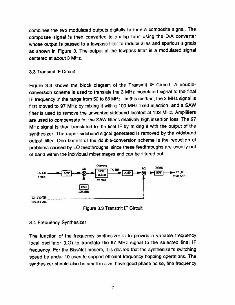
3.3 Transmit IF Circuit
Figure 3.3 shows the block diagram of the Transmit IF Circuit. A double-
conversion scheme is used to translate the 3 MHz modulated signal to the final
IF frequency in the range from 52 to 88 MHz. In this method, the 3 MHz signal is
first moved to 97 MHz by mixing it with a 100 MHz fixed injection, and a SAW
filter is used to remove the unwanted sideband located at 103 MHz. Amplifiers
are used to compensate for the SAW filter's relatively high insertion loss. The 97
MHz signal is then translated to the final IF by mixing it with the output of the
synthesizer. The upper sideband signal generated is removed by the wideband
output filter. One benefit of the double-conversion scheme is the reduction of
problems caused by LO feedthroughs, since these feedthroughs are usually out
of band within the individual mixer stages and can be filtered out.
(Nmow)m;:_--'l, zx_m: ,----, _ _')
3MHz -88 IVH-]z
10oM]Bz
TX_SYN'n-I
149-155
Figure 3.3 Transmit IF Circuit
3.4 Frequency Synthesizer
The function of the frequency synthesizer is to provide a variable frequency
local oscillator (LO) to translate the 97 MHz signal to the selected final IF
frequency. For the BissNet modem, it is desired that the synthesizer's switching
speed be under 10 usec to support efficient frequency hopping operations. The
synthesizer should also be small in size, have good phase noise, fine frequency

step size on the order of 500 Hz, and low spurious signal generation of -50 dBc
or better.
Some of the synthesizer design methods found in the open literature include
Direct Digital Synthesis (DDS), Phase-Locked Loop (PLL), DDS-PLL hybrid,
direct mixing, and FractionaI-N. After studying and evaluating these methods, it
became apparent that they are not suitable for the BissnNet modem due to
speed, frequency resolution, size, and complexity problems.
To solve the synthesizer design problem, an alternate approach was
developed, which uses a DDS circuit and a x9 frequency multiplier. Figure 3.4
shows the block diagram of the frequency synthesizer.
16.55-20.55 MI_
STEL1 I?SA J
I1_ TX S_"rttC(_?'_OLS _ FPJEQMULT 149-185 MHz
Figure 3.4 Frequency Synthesizer
Among the virtues of DDS circuits are fast switching times, low phase noise,
and fine frequency resolution, but its relatively high spurious output content is a
major concern. The nonlinear characteristics of the D/A converter used is the
major cause of spurious signal generation. Using a DDS chip that has 10 or
more output bits, a low-glitch high performance D/A converter, and good circuit
design practices, the DDS circuit can be designed and built to have spurious
signals greater than 55 dB below the desired output.
3.5 Transmit Controller
The Transmit Controller provides interface functions with the TDMA terminal
and control various blocks within the modulator. The number of interface signals
are designed to be as small as practical, although this may make the transfer of
information take several passes to complete. For instance, when the TDMA
terminal commands the modulator to tune to a particular IF carrier frequency,

the frequency word may be 24 bits long while the interface data path is only 8
bits wide. In this situation, the frequency word requires 3 passes to complete the
transfer.
4. Demodulator
Figure 4 shows the block diagram of the demodulator. At the input of the
demodulator, the IF signals are applied to the Receive IF Circuit to translate the
selected IF carrier to the 3 MHz low IF. The 3 MHz signal is then amplified by
the AGC amplifier to the appropriate level for A/D conversion.
Figure 4 Demoduator Block Diagram
The AGC amplifier is designed to handle a 30 dB input dynamic range. The
AGC amplifier's output is digitized by the ND converter at 8 times the symbol
rate. In setting the input level to the ND converter, some headroom is provided
to reduce the probability of overloading the ND converter during peaks in the
input signal.

The digitized signal is next mixed with the 3 MHz local quadrature carders in the
Carrier Circuit to generate a pair of outputs that contain the desired I and Q
baseband signals. The outputs of the Carrier Circuit are filtered by the Receive
Data Filters for matched filtering and to remove the unwanted products
generated in the mixing process. The resulting outputs are the desired I and Q
baseband signals at 2 times the symbol rate. Using these baseband signals,
the carrier phase, timing, and AGC errors are computed to update the various
loops for synchronization and AGC level adjustment.
For burst acquisition, a special circuit based on open-loop techniques is used to
estimate the carder, timing, and AGC errors during the preamble portion of the
burst. These estimates are subsequently loaded into the loops for closed-loop
operation.
4.1 Receive IF Circuit
Figure 4.1 shows the block diagram of the Receive IF Circuit. At the input, the IF
signals are passed to a wideband bandpass filter to reject image signals and
reduce out-of-band energy. The output of the wideband filter is then mixed with
the output of the frequency synthesizer to move the selected IF carrier to 97
MHz.
M1 97MHz
I (Nanow)_M2_
L_ SAW aL_u_ t _ RX_LIF
97MI-Iz
1
Figure 4.1 Receive IF Circuit
l0

A medium bandwidth filter is then used to decrease the number of IF carders
and composite signal power presented to the following amplifier. This reduces
the intercept requirements and the amount of intermodulation (IM) products
generated in the amplifier. A SAW filter is next used to reject adjacent channels
and to improve signal-to-noise ratio. The following amplifier boosts the signal
attenuated by the SAW filter. The narrowband filtered signal is then mixed with
the 100 MHz fixed injection signal to translate the 97 MHz signal to the 3 MHz
low IF. The 3 MHz signal is next passed through a Iowpass filter to remove the
upper sideband and to limit the bandwidth of the signal before A/D conversion.
4.2 Carder Circuit
Referring to Figure 4.2, the Carrier Circuit consists of a Numerically Controlled
Oscillator and Modulator (NCOM), a phase detector, and a loop filter. The
sampled 3 MHz low IF signal from the A/D converter is mixed with the
quadrature mixer to generate a pair of outputs that contain the desired I and Q
baseband signals and other unwanted products. Since the mixing process is
done digitally, the I/Q amplitude and phase imbalance problems are minimal.
Furthermore, any residual DC offset in the analog signal path will have little
effect on the demodulator performance, since the DC offset will be translated to
3 MHz in the mixing process and filtered out by the subsequent Receive Data
Filters.
11

(N= =md)
E
Figure 4.2 Carrier Circuit
The phase detector uses the I and Q data detection samples from the Receive
Data Filters' outputs to compute the carrier phase error, which is then passed to
the loop filter for signal averaging. The loop filter consists of two paths whose
outputs are summed together. One of the paths contains a bit shifter and an
accumulator, and the other path contains just a bit shifter. The bit shifter is used
to scale the phase error from the phase detector, and the accumulator is used
for error averaging. By appling the output of the loop filter to the NCOM, the
frequency of the oscillators in the NCOM is changed to reduce any phase error.
The accumulator output of the loop filter contains frequency error information,
which is passed to the TDMA terminal for uplink frequency correction.
4.3 Receive Data Filters
Figure 4.3 shows the block diagram of the Receive Data Filters. They contain
programmable Finite Impulse Response (FIR) filter blocks whose frequency
response can be changed quickly by using a different set of coefficients stored
internally. Since the preamble portion of the burst occupies only a narrow
12

portion of the modulated signal bandwidth, the filter blocks are programmed toexhibit a narrow bandpass response to increase the signal-to-noise ratio. Theyare then switched to have a 40% root-Raised Cosine response when
acquisition phase is complete. The outputs of the I and Q FIR filter blocks are
scaled by the digital AGC signal to make the averaged outputs of the Receive
Data Filters remain relatively constant.
Figure 4.3 Receive Data Filters
4.4 Timing Circuit
The Timing Circuit is used to adjust the phase of ND clock so that optimum
sampling instants for the I and Q baseband outputs are obtained. Referring to
Figure 4.4, timing error is computed by the timing error detector using data
transition information in the baseband I and Q outputs. The error signal is
scaled and used to control the frequency of the DDS chip. The DDS output is
then converted to analog form using the D/A converter and a Iowpass filter.
Finally, the voltage comparator is used to convert the Iowpass filter output to
generate the ND clock whose frequency is 8 times the symbol rate.
13

T_J_ST
S6_.,m
SGW_GE
]O
qO10
_ _vl=m_ I .v_,, . -
I_TA
_Ct.E
p,X ¢'J_
Figure 4.4 Timing Circuit
4.5 AGC Circuit
Figure 4.5 shows the block diagram of the AGC Circuit. This circuit accepts
inputs from a number of sources. In the burst acquisition phase, the output from
the AGC estimator is used. When in tracking phase, the outputs from the A/D
converter and the Receive Data Filters are used. There are two outputs from the
AGC circuit, one is for analog AGC and the other for digital AGC. The analog
AGC is used to control the AGC amplifier so that the input signal does not
overload the A/D converter. In the presence of large adjacent channel signals,
the desired signal may be greatly suppressed. To compensate for the reduced
amplitude of the desired signal after data filtering, digital AGC is used to
increase the signal back to the appropriate level.
IE,I0, QE, QO
AD_DATA
AGC EST
CONTROLS
EPLD
AGCCTRL
A AGC
Figure 4.5 AGC Circuit
14
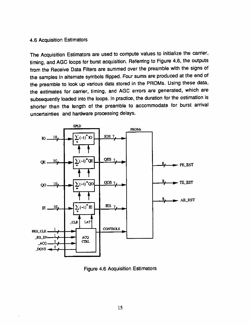
4.6 Acquisition Estimators
The Acquisition Estimators are used to compute values to initialize the carrier,
timing, and AGC loops for burst acquisition. Referring to Figure 4.6, the outputs
from the Receive Data Filters are summed over the preamble with the signs of
the samples in alternate symbols flipped. Four sums are produced at the end of
the preamble to look up various data stored in the PROMs. Using these data,
the estimates for carrier, timing, and AGC errors are generated, which are
subsequently loaded into the loops. In practice, the duration for the estimation is
shorter than the length of the preamble to accommodate for burst arrival
uncertainties and hardware processing delays.
SRX_CLK I
_P__HN 1 /
ACQ 1 /
EPLD
I i
--I
C'ONTROI_
_ ACQ
_ C'nlL
PROMs
w
_ _ PE_EST
8/ _-- TE_Egr
/ _ AE_EST
Figure 4.6 Acquisition Estimators
15

4.7 Frequency Synthesizer
This is the same design as used in the modulator.
4.8 Receive Controller
This circuit is used to provide the same functions as the Transmit Controller.
5.0 Conclusion
In this report, a frequency-hop burst modem design based on commerically
available chips is presented. It is shown that the key features that allow the
implementation of reliable burst modems include the availability of robust
algorithms for accurate carrier phase, timing phase, and AGC estimations, a
modem whose various loops can be initialized with the estimates, and the
developement of fast-switching frequency synthesizer.
With the rapid advances in analog and digital communications ICs, it is
expected that more functions will be integrated onto these parts in the near
future. In addition, custom ASICs can also be developed to address the areas
not covered by the other ICs. Using the commerical chips and custom ASICs,
lower-cost, compact, reliable, and high-performance modems can be built for
demanding satellite communication applications.
16


Form ApprovedREPORT DOCUMENTATION PAGE OMB No.0704-0188
Public reportingburden tot this coflection04 informationis estimated Io average 1 hour per response, includingthe timelot reviewin_.instructions,searchingexistingdata sources.galledng and maJntarningthe data needed, and completingand reviewingthe collectionOfinformation. Send commentsregarding ms burdene_imate of any offier espanl of thiscofle_icn ol information,includingsuggestions fo¢ reducingthis burden, 1oWashingtonHeadquartersServices. Directoraletor IrdormaflonOperations and Repocts,1215 JeffecsonDavis Highway, Suite 1204, Arlington.VA 2220Q-4302, and to the Office Of Managementand Budget, Paperwork ReductionProject (0704-0188), Washington. DC 20503.
1. AGENCY USE ONLY (Leave blank)
4. TITLE AND SUBTITLE
Burst Mode ASIC-Based Modem
2. REPORT DATE
January 1997
e. AUTHOR(S)
COMSAT Laboratories
7. PERFORMING ORGANIZATION NAME(S) AND ADDRESSEES)
COMSAT Laboratories22300 COMSAT Drive
Clarksburg, Maryland 20871
9. SPONSORING/MONITORINGAGENCYNAME(S)ANDADDRESS{ES)
National Aeronautics and Space AdministrationLewis R_h Center
Cleveland, Ohio 44135-3191
3. REPORT TYPE AND DATES COVERED
Final Contractor Report5. FUNDING NUMBERS
WU--632-50-5CC-NAS 3-27356
8. PERFORMING ORGANIZATION
REPORT NUMBER
E-10615
10. SPONSORING/MONFrORINGAGENCY REPORT NUMBER
NASA CR-202315
11. SUPPLEMENTARY NOTES
Project Manager, Nitin J. Soni, Space Communications Division, NASA Lewis Research Center, organization code 5650,
(216) 433--6591.
12a. DISTRJ BUTIONFAVAILABILITY STATEMENT
Unclassified - Unlimited
Subject Category 32
This publication is available from the NASA Center forAeroSpaee Information, (301) 621--0390.
12b. DISTRIBUTION CODE
13. ABSTRACT (Maximum 200 words)
The NASA Lewis Research Center is sponsoring the Advanced Communication Technology Insertion (ACTION) for
Commercial Space Applications program. The goal of the program is to expedite the development of new technology with
a clear path towards productization and enhancing the competitiveness of U.S. manufacturers. The industry has made
significant investment in developing ASIC-based modem technology for continuous-mode applications and has madeinvestigations into fast, reliable acquisition of burst-mode digital communication signals. With rapid advances in analog
and digital communications ICs, it is expected that more functions will be integrated onto these parts in the near future. In
addition custom ASICs can also be developed to address the areas not covered by the other ICs. Using the commercial
chips and custom ASICs, lower-cost, compact, reliable, and high-performance modems can be built for demanding
satellite communication application. This report outlines a frequency-hop burst modem design based on commercially
available chips.
14. SUBJECT TERMS
Burst mode; QPSK; Modulator; Demodulator; Transmit filters; Receive filters; ASIC
17. SECURITY CLASSIFICATION
OF REPORT
Unclassified
NSN 7540-01-280-5500
18. SECURITY CLASSIFICATION
OF THIS PAGE
Unclassified
19. SECURITY CLASSIFICATION
OF ABSTRACT
Unclassified
15. NUMBER OF PAGES
]816. PRICE CODE
A03
20. LIMITATION OF ABSTRACT
Standard Form 298 (Rev. 2-89)
Prescribed by ANS ! Std. Z39-18298-102