c 2017 john a. krol
TRANSCRIPT

c© 2017 John A. Krol

NONRECIPROCAL MICROWAVE DEVICES USING PARAMETRICFREQUENCY CONVERSION
BY
JOHN A. KROL
THESIS
Submitted in partial fulfillment of the requirementsfor the degree of Master of Science in Electrical and Computer Engineering
in the Graduate College of theUniversity of Illinois at Urbana-Champaign, 2017
Urbana, Illinois
Adviser:
Assistant Professor Songbin Gong

ABSTRACT
This thesis endeavors to characterize the performance of nonreciprocal mi-
crowave devices enabled by parametric frequency conversion. Although such
devices have been explored somewhat superficially in the 1960s, resurgent
interest in low-noise nonreciprocal components has motivated new research
in parametric frequency conversion. In particular, this work explores the
contributions of nonidealities to performance degradation of a parametric gy-
rator. Expressions are developed for loss and noise performance contributed
by nonideal components constituting the gyrator, and simulations are used
to verify the findings. The gyrator is then used to construct a circulator,
and its performance’s dependence on the same nonidealities is evaluated. A
simulated design example is used to demonstrate a practical realization of
such a circulator.
ii

“Du Sterne hellster, o wie schon verkundest du den Tag! Wie schmuckst du
ihn, o Sonne du, des Weltalls Seel’ und Aug’! Ihr’ Elemente, deren Kraft,
stets neue Formen zeugt...”
-Gottfried van Swieten
From the libretto to Haydn’s “Die Schopfung”
iii
ACKNOWLEDGMENTS
The author wishes to express gratitude to Dr. Gong for his tireless efforts
in shaping this thesis into a respectable document. Special thanks also to
Dr. Pete Dragic for encouraging me to pursue my master’s degree and for
introducing me to the world of academic research. Thanks also to my family,
especially my mother, Judy, and my father, Steve, who both taught me the
value of hard work and encouraged my studies at every moment. Thanks
also to my uncle Dan, who first sparked my interest in electrical engineering.
Finally, thanks to my girlfriend, Peng, whose unmatched skill at the piano has
filled my life with the sounds of Schumann, Brahms and Beethoven.
iv
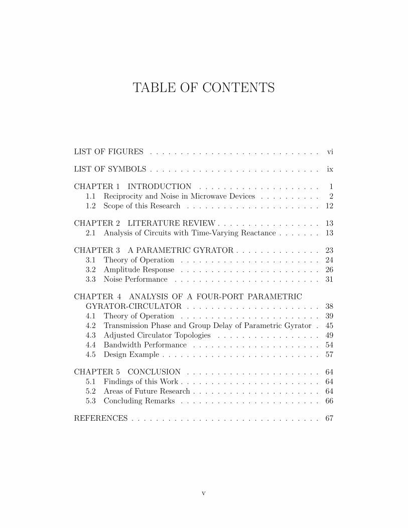
TABLE OF CONTENTS
LIST OF FIGURES . . . . . . . . . . . . . . . . . . . . . . . . . . . . vi
LIST OF SYMBOLS . . . . . . . . . . . . . . . . . . . . . . . . . . . . ix
CHAPTER 1 INTRODUCTION . . . . . . . . . . . . . . . . . . . . 11.1 Reciprocity and Noise in Microwave Devices . . . . . . . . . . 21.2 Scope of this Research . . . . . . . . . . . . . . . . . . . . . . 12
CHAPTER 2 LITERATURE REVIEW . . . . . . . . . . . . . . . . . 132.1 Analysis of Circuits with Time-Varying Reactance . . . . . . . 13
CHAPTER 3 A PARAMETRIC GYRATOR . . . . . . . . . . . . . . 233.1 Theory of Operation . . . . . . . . . . . . . . . . . . . . . . . 243.2 Amplitude Response . . . . . . . . . . . . . . . . . . . . . . . 263.3 Noise Performance . . . . . . . . . . . . . . . . . . . . . . . . 31
CHAPTER 4 ANALYSIS OF A FOUR-PORT PARAMETRICGYRATOR-CIRCULATOR . . . . . . . . . . . . . . . . . . . . . . 384.1 Theory of Operation . . . . . . . . . . . . . . . . . . . . . . . 394.2 Transmission Phase and Group Delay of Parametric Gyrator . 454.3 Adjusted Circulator Topologies . . . . . . . . . . . . . . . . . 494.4 Bandwidth Performance . . . . . . . . . . . . . . . . . . . . . 544.5 Design Example . . . . . . . . . . . . . . . . . . . . . . . . . . 57
CHAPTER 5 CONCLUSION . . . . . . . . . . . . . . . . . . . . . . 645.1 Findings of this Work . . . . . . . . . . . . . . . . . . . . . . . 645.2 Areas of Future Research . . . . . . . . . . . . . . . . . . . . . 645.3 Concluding Remarks . . . . . . . . . . . . . . . . . . . . . . . 66
REFERENCES . . . . . . . . . . . . . . . . . . . . . . . . . . . . . . . 67
v

LIST OF FIGURES
1.1 Two-port network. Ports 1 and 2 are driven by sources aand b, respectively. Each source is connected to the two-port via a waveguide with modal fields shown. Surface Sencloses the two-port. . . . . . . . . . . . . . . . . . . . . . . . 4
1.2 System-level representation of various circulators. The curvedarrows represent the sense of rotation. . . . . . . . . . . . . . 7
1.3 An isolator constructed from a circulator. The value of theresistance is the same as the system impedance. . . . . . . . . 9
1.4 (a) Tellegen’s symbol for a gyrator. (b) Three-port circu-lator from gyrator. (c) Four-port circulator from gyrator. . . . 10
1.5 A full-duplex transceiver. A circulator separates the trans-mit and receive chains. . . . . . . . . . . . . . . . . . . . . . . 11
2.1 Spectra of non-inverting and inverting parametric converter. . 182.2 Norton equivalent circuit of either non-inverting or invert-
ing parametric converter. The filters are ideally open atthe marked frequency and short otherwise. The nonlinearcapacitor has an admittance matrix of either equation 2.27or 2.34. . . . . . . . . . . . . . . . . . . . . . . . . . . . . . . . 20
3.1 Component-level diagram of parametric gyrator. . . . . . . . . 243.2 Thevenin equivalent circuit of non-inverting parametric con-
verter. The nonlinear capacitor can be represented by theimpedance matrix of equation 3.10. . . . . . . . . . . . . . . . 27
3.3 Insertion loss of gyrator for various conversion ratios withψ fixed at 0.25. . . . . . . . . . . . . . . . . . . . . . . . . . . 31
3.4 Equivalent noise model of both upconverter and downconverter. 323.5 Noise figure for a fixed modulation parameter (ψ = 0.25)
for an upconverter (F↑) and a downconverter (F↓). . . . . . . . 353.6 Noise figure for a fixed frequency ratio ( ω+
ωIF= 3) for an
upconverter (F↑) and a downconverter (F↓). . . . . . . . . . . 363.7 Noise figure of gyrator with various Qd with ψ fixed at 0.25. . 37
4.1 (a) System level diagram of hybrid coupler. (b) Waveguidemagic tee. (c) Microstrip ratrace coupler. . . . . . . . . . . . . 40
vi

4.2 Graphical representation of operation of right-handed four-port parametric circulator. All quantities shown are inphasor form. . . . . . . . . . . . . . . . . . . . . . . . . . . . . 41
4.3 Graphical representation of operation of left-handed four-port parametric circulator. . . . . . . . . . . . . . . . . . . . . 44
4.4 Expanded model of parametric gyrator that explicitly ac-counts for the effects of the necessary filters. The compo-nents ZL and ZR can both be described by the matrix of3.10 by substituting the value of θ with α and β, respec-tively. As before, these quantities denote the LO phase. . . . . 46
4.5 Computed values of ∠AL21, ∠AL12, ∠AR21, and ∠AR12
alongside modulator/demodulator transducer gain. Thegain is normalized to the ideal Manley-Rowe value: fp+f
f
for an upconverter and ff+fp
for a downconverter. . . . . . . . 50
4.6 Transmission phase characteristic in each direction over the3 dB bandwidth of the gyrator. . . . . . . . . . . . . . . . . . 50
4.7 (a) Adjusted four-port circulator topology and (b) approx-imation of three-port circulator. The phase compensationcan be used to tune the center frequency of the gyrator tothe center frequency of the hybrids and dividers. The de-lay balance has a time delay equal to the combined delayof the gyrator and the phase compensation. . . . . . . . . . . 51
4.8 (a) Symbol for a quasi-circulator. (b) Full-duplex commu-nication system with quasi-circulator. . . . . . . . . . . . . . . 53
4.9 Isolation performance of idealized four-port circulator us-ing ratrace hybrids. The isolation characteristic is not iden-tical between all port pairs. . . . . . . . . . . . . . . . . . . . 55
4.10 Transmission line realization of branchline coupler. Alllines are 90 in electrical length. . . . . . . . . . . . . . . . . . 56
4.11 Isolation performance of idealized four-port circulator us-ing branchline hybrids. The isolation characteristic is notidentical between all port pairs. . . . . . . . . . . . . . . . . . 56
4.12 Topology of the broadbanded circulator. All transmissionlines are 90 in electrical length. . . . . . . . . . . . . . . . . . 57
4.13 Isolation performance of idealized four-port circulator. Theisolation characteristic is not identical between all port pairs. . 57
4.14 Noise figure of the gyrator for various LO frequencies. Thedynamic quality factor Qd is approximately 160 for thehighest supported modulation parameter. . . . . . . . . . . . . 58
4.15 Four-port circulator insertion loss and isolation betweenport pairs for increasing levels of gyrator insertion loss. . . . . 59
vii

4.16 Keysight ADS simulation of gyrator. LSSP simulation per-forms the function of a typical harmonic balance simula-tion, but makes computation of quantities like insertionloss and transducer gain simpler, especially when the fre-quency is swept over some range. . . . . . . . . . . . . . . . . 60
4.17 Simulation of gyrator insertion loss (magnitude of S21, S12)and return loss (magnitude of S11, S22) for varying ψ. . . . . . 61
4.18 Simulation of gyrator insertion loss and transmission phaseover frequency. . . . . . . . . . . . . . . . . . . . . . . . . . . 62
4.19 Magnitude of S21 and S12 of the gyrator-circulator. . . . . . . 624.20 Keysight ADS simulation schematic for four-port paramet-
ric circulator. . . . . . . . . . . . . . . . . . . . . . . . . . . . 63
viii

LIST OF SYMBOLS
Yij Admittance Parameter for Ports i and j
ω Angular Frequency (ω = 2πf)
GA Available Gain
I Current
C1 Dynamic Capacitance at Frequency fLO
ξ Dynamic Loss Factor
Qd Dynamic Quality Factor
¯σ Electric Conductivity Tensor
~J Electric Current Density
~E Electric Field Intensity
¯ε Electric Permittivity Tensor
Zij Impedance Parameter for Ports i and j
IL Insertion Loss
ωIF Intermediate Angular Frequency (ω = 2πfIF)
ω− Inverting Converted Angular Frequency (ω = 2πf−)
f Linear Frequency
ωLO Local Oscillator Angular Frequency (ω = 2πfLO)
~M Magnetic Current Density
~H Magnetic Field Intensity
¯µ Magnetic Permeability Tensor
ψ Modulation Parameter
F Noise Factor
ix

NF Noise Figure (NF = 10 logF )
ω+ Non-inverting Converted Angular Frequency (ω = 2πf+)
W Power (W = V I∗)
GP Power Gain
Sij Scattering Parameter for Ports i and j
Rc Series Loss Resistance
SNR Signal-to-Noise Ratio
C0 Static Capacitance
GT Transducer Gain
V Voltage
e Waveguide Modal Electric Field Distribution
h Waveguide Modal Magnetic Field Distribution
x

CHAPTER 1
INTRODUCTION
Electrical circuits with variable parameters are known as parametric circuits.
Most often, the term is used to describe circuits containing a lossless element
with a parameter that varies in time. One example of this would be the
variation of the reverse-bias capacitance of an ideal varactor diode by an
external voltage source. In such a circuit, an excitation of one frequency can
be used to generate signals of many other frequencies. Although the concept
of parametric excitation was first observed in a mechanical system by Michael
Faraday [1] in 1831, it was first applied to electrical circuits in 1892 by G.
F. FitzGerald [2]. Throughout the 20th century, parametric circuits were
utilized often in high-sensitivity receiver systems for satellite communications
[3, 4, 5] or as amplifiers in radar systems [6, 7, 8] due to their unique low-noise
properties and their ability to operate at microwave frequencies. Before the
invention of the high electron mobility transistor (HEMT) [9], parametric
amplifiers built with varactor diodes were the only solid-state technique to
amplify a signal at microwave frequencies. Although parametric circuits fell
largely into obscurity with the invention of the HEMT, they have found
new applications in modern times as the demand has grown for small, low-
noise nonreciprocal microwave elements readily realized in integrated form.
This demand comes largely from the communications industry, where such
components are needed to achieve full-duplex communication, also called
simultaneous transmit-and-receive (STAR). In this scheme, a transceiver can
transmit and receive information at the same time and the same frequency.
This is in contrast to time domain duplex, where transmission and reception
are performed at different times, or frequency domain duplex, where each is
done at different frequencies. Intuitively, STAR could be used to double the
bandwidth of conventional transceivers.
1

1.1 Reciprocity and Noise in Microwave Devices
The behavior of signals traveling in different directions inside a microwave
device is known as the reciprocity of the device. When discussing the reci-
procity of the device, it is convenient to describe the device as an n-port
network, where a port is a pair of terminals. In this case, the formalism of
scattering parameters can be used to classify the device. For a reciprocal
device, the scattering parameters must satisfy the relation shown in equation
1.1.
Sij = Sji, i 6= j, i = 1, 2, 3...n, j = 1, 2, 3...n (1.1)
This means that if some voltage Va is applied at some port i and a corre-
sponding voltage Vb is measured at port j, then the same voltage Vb should
be measured at port i if Va is applied to port j. For a nonreciprocal device,
relation in equation 1.1 is not satisfied for at least one pair of ports. This
means that for at least one pair of ports i and j, if some voltage Va is applied
to port i and Vb is measured at port j, it will be observed that some voltage
Vc 6= Vb is measured at port i if Va is now applied to port j. The existence
of these two types of devices can be demonstrated from Maxwell’s equations
using the reciprocity theorem [10].
1.1.1 Reciprocity Theorem and Relation to ElectricalCircuits
In the study of electromagnetic fields and waves, there exists an important
theorem relating the behavior of two independent fields generated by two
independent sources. This theorem originates from the fact that both fields
are governed by Maxwell’s equations and is known as the reciprocity theo-
rem. Although the theorem exists in several forms and can be generalized to
an arbitrary number of independent sources, the form known as the Lorentz
reciprocity theorem is most amenable to the description of circuits. The the-
orem can be derived by first considering two independent electromagnetic
fields: ( ~E1, ~H1) and ( ~E2, ~H2). Each of these field quantities is a vector in
2

three-dimensional space, and thus can be represented with a column vector.
In the context of an electrical circuit, such as a two-port device, these inde-
pendent fields could represent a signal incident upon port one and a signal
incident upon port two. These fields follow Ampere’s and Faraday’s laws,
meaning
∇× ~E1 = −jω ¯µ ~H1 − ~M1 (1.2)
∇× ~H1 = (jω¯ε+ ¯σ) ~E1 + ~J2 (1.3)
∇× ~E2 = −jω ¯µ ~H2 − ~M2 (1.4)
∇× ~H2 = (jω¯ε+ ¯σ) ~E2 + ~J2 (1.5)
In the most general case, the material parameters ¯µ, ¯ε and ¯σ are expressed
as tensors with positional dependence. In rectangular coordinates,
ε(x, y, z) =
εxx(x, y, z) εxy(x, y, z) εxz(x, y, z)
εyx(x, y, z) εyy(x, y, z) εyz(x, y, z)
εzx(x, y, z) εzy(x, y, z) εzz(x, y, z)
µ(x, y, z) =
µxx(x, y, z) µxy(x, y, z) µxz(x, y, z)
µyx(x, y, z) µyy(x, y, z) µyz(x, y, z)
µzx(x, y, z) µzy(x, y, z) µzz(x, y, z)
σ(x, y, z) =
σxx(x, y, z) σxy(x, y, z) σxz(x, y, z)
σyx(x, y, z) σyy(x, y, z) σyz(x, y, z)
σzx(x, y, z) σzy(x, y, z) σzz(x, y, z)
The physical reason for this is that, in general, material parameters can
be dependent on the direction of propagation of EM waves. This is referred
to as anisotropy. If these material parameters are spatially dependent, this
is referred to as inhomogeneity. Rearranging equations 1.2, 1.3, 1.4 and 1.5
yields
∇· ( ~H2× ~E1) = −jω¯ε ~E1 · ~E2 + ¯σ ~E1 · ~E2 + jω ¯µ ~H2 · ~H1 + ~E1 · ~J2 + ~H2 · ~M1 (1.6)
∇· ( ~H1× ~E2) = −jω¯ε ~E2 · ~E1 + ¯σ ~E2 · ~E1 + jω ¯µ ~H1 · ~H2 + ~E2 · ~J1 + ~H1 · ~M2 (1.7)
3
For a symmetric tensor, its product with a vector is commutative, which is
to say ¯α ~A = ~A ¯α, and thus if ¯µ, ¯ε and ¯σ are all symmetric, then subtracting
equation 1.7 from 1.6 yields
∇ · ( ~H2 × ~E1 − ~H1 × ~E2) = ~E1 · ~J2 + ~H2 · ~M1 − ~E2 · ~J1 − ~H1 · ~M2 (1.8)
Materials that satisfy this condition are known as reciprocal materials. If
equation 1.8 is integrated over a region of finite volume V that contains no
sources (i.e. ~Ji = 0, ~Mi = 0), then applying the divergence theorem yields
1.9
S
( ~E1 × ~H2) · n dS =
S
( ~E2 × ~H1) · n dS (1.9)
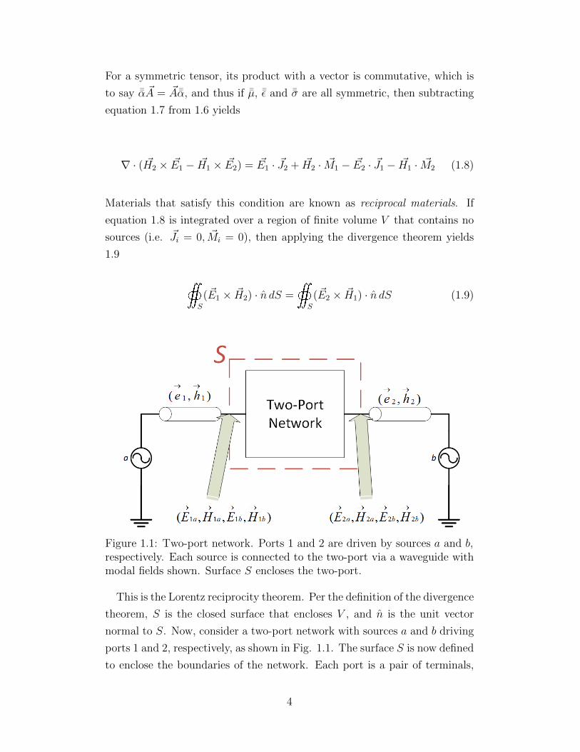
Figure 1.1: Two-port network. Ports 1 and 2 are driven by sources a and b,respectively. Each source is connected to the two-port via a waveguide withmodal fields shown. Surface S encloses the two-port.
This is the Lorentz reciprocity theorem. Per the definition of the divergence
theorem, S is the closed surface that encloses V , and n is the unit vector
normal to S. Now, consider a two-port network with sources a and b driving
ports 1 and 2, respectively, as shown in Fig. 1.1. The surface S is now defined
to enclose the boundaries of the network. Each port is a pair of terminals,
4

and can be addressed by some type of waveguide. If the waveguides are
constructed from perfect electrical conductors, the fields excited in each due
to some source can be expressed in terms of each waveguide’s transverse
modal fields. If the waveguide connecting port 1 has modal fields (~e1, ~h1)
and the waveguide at port 2 has modal fields (~e2, ~h2), then the fields at each
port due to each source can be linearly related to the modal fields as shown
in 1.10.
~E1a = V1a~e1, ~H1a = I1a~h1 (1.10a)
~E1b = V1b~e1, ~H1b = I1b~h1 (1.10b)
~E2a = V2a~e2, ~H2a = I2a~h2 (1.10c)
~E1b = V2b~e2, ~H2b = I2b~h2 (1.10d)
Each field is denoted with a two-part subscript with the first part being the
port and the second being the source. For example, ~E1a is the electric field
at port 1 excited by source a. Now, 1.10 can be substituted into 1.9 to
obtain
(V1aI1b − V1bI1a)S
(~e1 × ~h1) · n dS
+ (V2aI2b − V2bI2a)S
(~e2 × ~h2) · n dS = 0 (1.11)
Comparing equations 1.10 and 1.9, then it can be seen that
S
(~e1 × ~h1) · n dS =
S
(~e2 × ~h2) · n dS = 1 (1.12)
and now equation 1.11 can be reduced to
(V1aI1b − V1bI1a) + (V2aI2b − V2bI2a) = 0 (1.13)
Next, one must consider the definition of the admittance matrix:
5

[I1
I2
]=
(Y11 Y12
Y21 Y22
)[V1
V2
](1.14)
Using this definition, equation 1.13 can be rewritten as
(V1aV2b − V1bV2a)(Y12 − Y21) = 0 (1.15)
Since sources a and b are independent, the total voltage at each port due
to each source can take on arbitrary values, and the only way to satisfy
equation 1.15 is to have Y21 = Y12. Although this is a proof for the admittance
matrix, the effect of reciprocity on the scattering matrix of this network can
be demonstrated without going into the definition of the scattering matrix
itself. It has been demonstrated that the relationship between Y and S
is
S12 =−2Z0Y12
∆(1.16a)
S21 =−2Z0Y21
∆(1.16b)
with ∆ as the determinant of the admittance matrix. Since Y12 = Y21, it is
clear that S12 = S21. The theorem of equation 1.9 can be generalized to an
arbitrary number of fields, meaning a reciprocal n-port network will have, for
i = 1, 2, 3...n, j = 1, 2, 3...n and i 6= j, Sij = Sji. As stated earlier, an n-port
network constructed with reciprocal materials follows this requirement. In
this work, it will be shown that networks with lossless, time-varying elements
can violate this theorem.
1.1.2 Nonreciprocal Devices
In microwave engineering, some designs require components that manipu-
late signals differently depending on their direction of propagation [10]. As
stated before, reciprocal devices have Sij = Sji, and therefore cannot per-
form these tasks. Instead, nonreciprocal devices are required. This section
6

describes three common devices to familiarize the reader with the utility of
nonreciprocal components.
1.1.2.1 Circulators
A circulator is a device that transmits signals from one port to the next in
a successive rotation , but blocks transmission in the opposite rotation. It is
also matched at all ports. Although a circulator can have n > 2 ports, three-
port and four-port circulators are the most common. The handedness of a
circulator is the rotation direction of circulation. A right-handed three-port
circulator circulates power in a succession of ports as 1 → 2 → 3 → 1. Its
scattering matrix is
S =
0 1 0
0 0 1
1 0 0
(1.17)
Figure 1.2: System-level representation of various circulators. The curvedarrows represent the sense of rotation.
A left-handed three-port circulator circulates power in a succession of ports
as 1→ 3→ 2→ 1. Its scattering matrix is
S =
0 1 0
0 0 1
1 0 0
(1.18)
Right-handed and left-handed four port circulators exist as well. Scattering
matrices for each are shown in equations 1.19 and 1.20, respectively.
7

S =
0 0 0 1
1 0 0 0
0 1 0 0
0 0 1 0
(1.19)
S =
0 1 0 0
0 0 1 0
0 0 0 1
1 0 0 0
(1.20)
Circulators in practice can impart any phase on signals, so the 1s in the
scattering matrices could be replaced by complex numbers with unity magni-
tude. Symbolic representations of each of these circulators are shown in Fig.
1.2. At microwave frequencies, the most common type of circulator is the
ferrite circulator, which employs the principle of Faraday rotation within a
magnetic material to create a nonreciprocal effect. Ferrite devices are bulky
and difficult to include in integrated circuits.
1.1.2.2 Isolators
An isolator is a two-port device that only allows transmission of a signal
in one direction. An ideal isolator can be described by the scattering ma-
trix
S =
(0 0
1 0
)(1.21)
Much like circulators, isolators are most often built with ferrite materials.
The functionality of an isolator can be achieved by terminating one of the
ports of a three-port circulator with a matched load. A schematic represen-
tation of this is shown in Fig. 1.3. Isolators suffer from the same limitations
circulators do, since their operation is very similar.
8
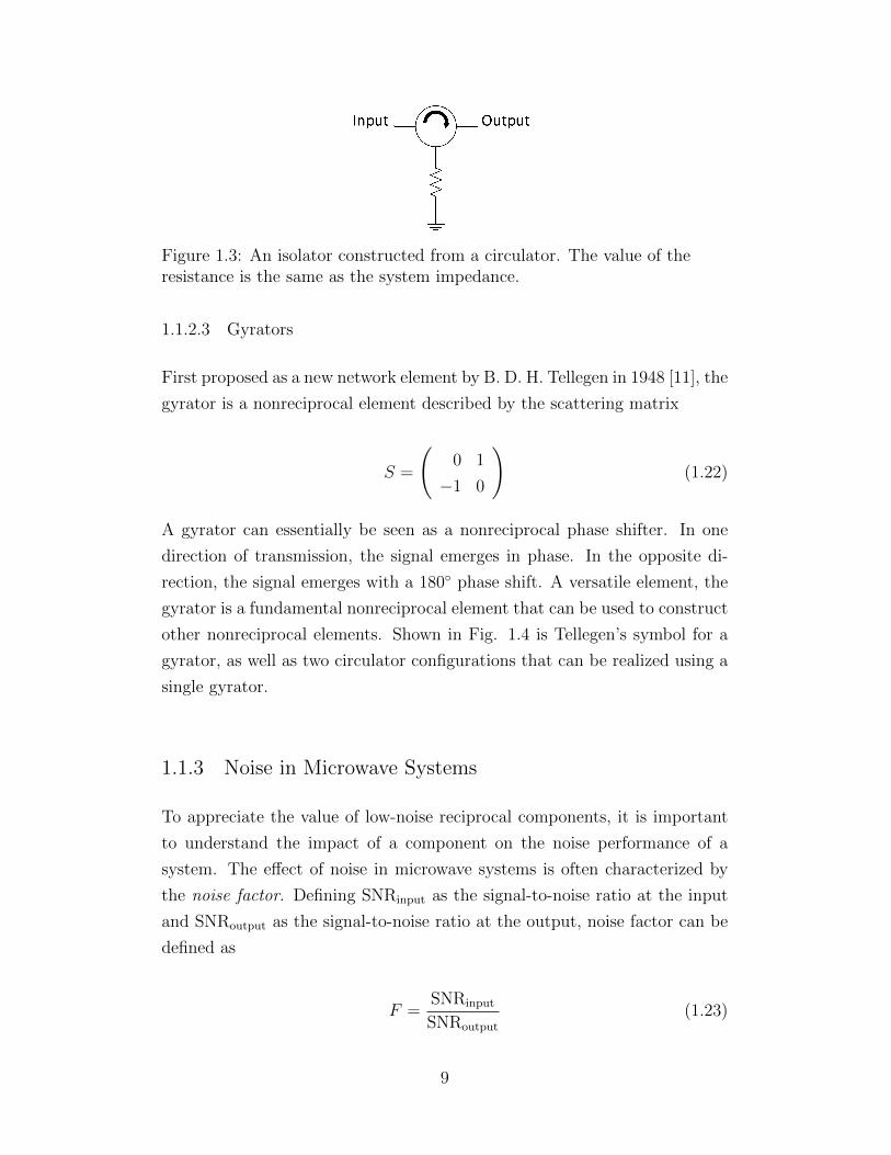
Figure 1.3: An isolator constructed from a circulator. The value of theresistance is the same as the system impedance.
1.1.2.3 Gyrators
First proposed as a new network element by B. D. H. Tellegen in 1948 [11], the
gyrator is a nonreciprocal element described by the scattering matrix
S =
(0 1
−1 0
)(1.22)
A gyrator can essentially be seen as a nonreciprocal phase shifter. In one
direction of transmission, the signal emerges in phase. In the opposite di-
rection, the signal emerges with a 180 phase shift. A versatile element, the
gyrator is a fundamental nonreciprocal element that can be used to construct
other nonreciprocal elements. Shown in Fig. 1.4 is Tellegen’s symbol for a
gyrator, as well as two circulator configurations that can be realized using a
single gyrator.
1.1.3 Noise in Microwave Systems
To appreciate the value of low-noise reciprocal components, it is important
to understand the impact of a component on the noise performance of a
system. The effect of noise in microwave systems is often characterized by
the noise factor. Defining SNRinput as the signal-to-noise ratio at the input
and SNRoutput as the signal-to-noise ratio at the output, noise factor can be
defined as
F =SNRinput
SNRoutput
(1.23)
9
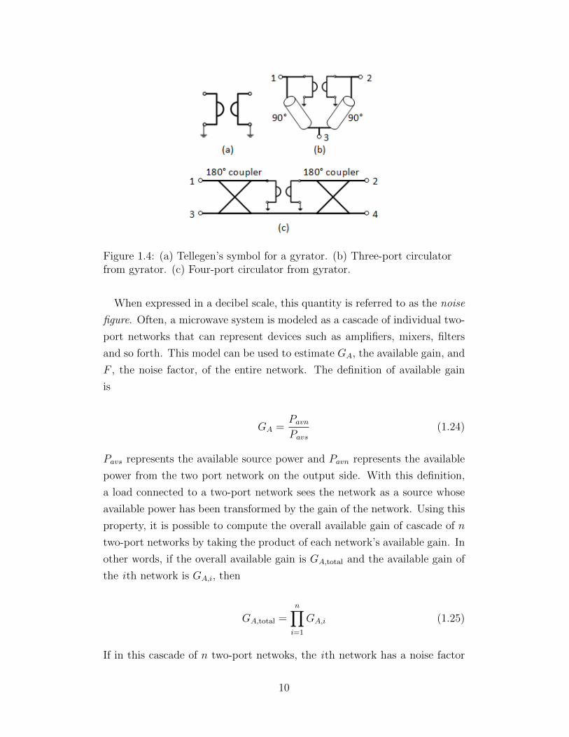
Figure 1.4: (a) Tellegen’s symbol for a gyrator. (b) Three-port circulatorfrom gyrator. (c) Four-port circulator from gyrator.
When expressed in a decibel scale, this quantity is referred to as the noise
figure. Often, a microwave system is modeled as a cascade of individual two-
port networks that can represent devices such as amplifiers, mixers, filters
and so forth. This model can be used to estimate GA, the available gain, and
F , the noise factor, of the entire network. The definition of available gain
is
GA =PavnPavs
(1.24)
Pavs represents the available source power and Pavn represents the available
power from the two port network on the output side. With this definition,
a load connected to a two-port network sees the network as a source whose
available power has been transformed by the gain of the network. Using this
property, it is possible to compute the overall available gain of cascade of n
two-port networks by taking the product of each network’s available gain. In
other words, if the overall available gain is GA,total and the available gain of
the ith network is GA,i, then
GA,total =n∏i=1
GA,i (1.25)
If in this cascade of n two-port netwoks, the ith network has a noise factor
10
of Fi, then the overall noise factor of the entire system [10] can be expressed
as
Ftotal = F1 +F2 − 1
GA,1
+F3 − 1
GA,1GA,2
+ ...+Fn − 1
GA,1GA,2GA,3...GA,n
(1.26)
The most critical result of this formula is that devices present near the
front-end of a microwave system contribute the most to the overall noise
factor of the system. It is therefore paramount to minimize the noise figure
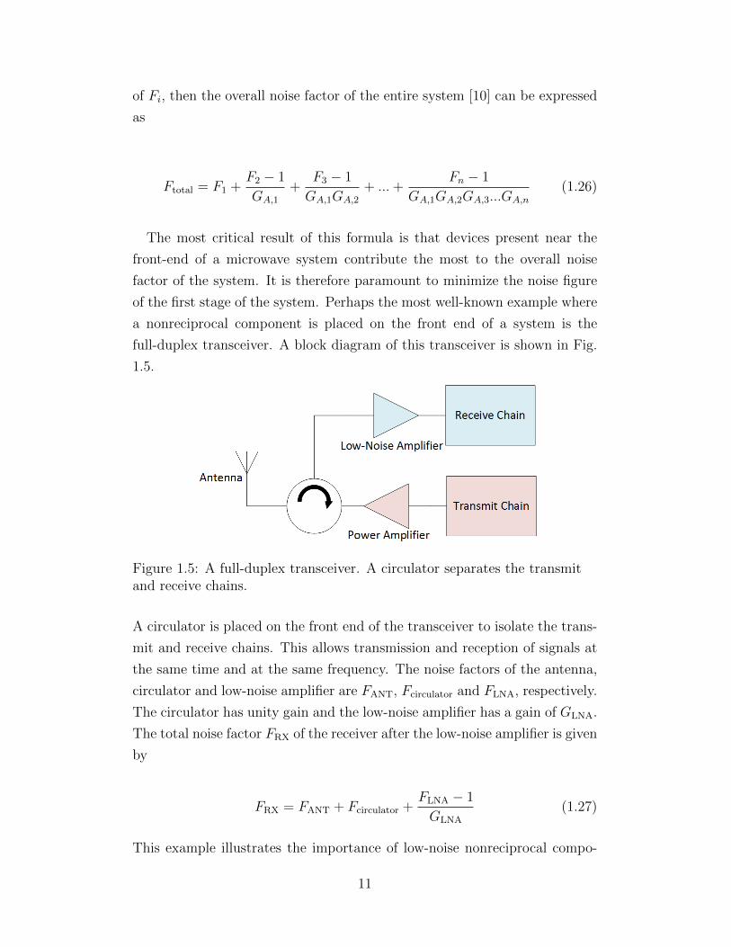
of the first stage of the system. Perhaps the most well-known example where
a nonreciprocal component is placed on the front end of a system is the
full-duplex transceiver. A block diagram of this transceiver is shown in Fig.
1.5.
Figure 1.5: A full-duplex transceiver. A circulator separates the transmitand receive chains.
A circulator is placed on the front end of the transceiver to isolate the trans-
mit and receive chains. This allows transmission and reception of signals at
the same time and at the same frequency. The noise factors of the antenna,
circulator and low-noise amplifier are FANT, Fcirculator and FLNA, respectively.
The circulator has unity gain and the low-noise amplifier has a gain of GLNA.
The total noise factor FRX of the receiver after the low-noise amplifier is given
by
FRX = FANT + Fcirculator +FLNA − 1
GLNA
(1.27)
This example illustrates the importance of low-noise nonreciprocal compo-
11

nents.
1.2 Scope of this Research
This thesis concerns the mathematical analysis of a gyrator constructed from
parametric devices. This particular gyrator was first explored by A. K. Ka-
mal [12] in 1960 with supporting experimental results, but only a first-order
analysis was performed demonstrating the principle of operation. This work
seeks to further explore the parametric gyrator by performing an analysis of
the effect of nonidealities of nonlinear reactance elements on the insertion loss
and noise performance. The results of this analysis are then used to estimate
the performance of the parametric gyrator when operating as a circulator.
The bandwidth of the circulator is explored, as well as various topologies
that can be utilized to physically realize it in both three- and four-port form.
Finally, a design example along with simulations is presented to demonstrate
the application of the theory presented in the construction of a parametric
circulator.
12
CHAPTER 2
LITERATURE REVIEW
In order to understand the application of parametric circuits to the creation
of nonreciprocal elements, an understanding of the operation of paramet-
ric circuits is necessary. In this section, the fundamentals of time-varying
reactance circuits are explored from the quintessential literature on the sub-
ject.
2.1 Analysis of Circuits with Time-Varying
Reactance
The seminal two-part paper by J. M. Manley and H. E. Rowe [13, 14] is the
fundamental reference in the design of circuits with time-varying reactance,
referred to as parametric circuits. In the first part, Manley uses a Fourier
expansion of the charge on a nonlinear capacitor to derive general energy re-
lations that characterize the power in all frequencies that are generated when
the capacitor is driven with two signals of two incommensurate frequencies.
In the second paper, Rowe confirms the findings of the first paper by ap-
proaching the nonlinear capacitor with small-signal circuit analysis. This
part contains information that is paramount in designing physical paramet-
ric circuits that are conjugately matched at all ports and provide bilateral
frequency conversion.
2.1.1 General Energy Relations
The analysis in both papers assumes the time-varying element is a capacitor
with a voltage v that is an arbitrary single-valued function of the charge,
13
q.
v = f(q) (2.1)
If two signals of frequencies ω0 and ω1 are applied to the capacitor, in general,
currents of frequencies ωmn = mω0 + nω1, where m and n take on all integer
values, will be generated. In this case, the time-varying charge q(t) flowing
through the capacitor can be expressed as a double Fourier series:
q(t) = q(ω0t, ω1t) =∞∑
m=−∞
∞∑n=−∞
Qmnej(mω0t+nω1t) (2.2a)
Qmn =1
4π2
2π
0
2π
0
q(ω0t, ω1t)e−j(mω0t+nω1t)d(ω0t)d(ω1t) (2.2b)
The voltage v(t) across the capacitor is a periodic function, as f(q(t)) is a
single-valued function. The current i(t) through the capacitor is also periodic,
as it is related to the charge as i(t) = dq(t)dt
. Thus, both can be expanded
using a Fourier series:
i(t) = i(ω0t, ω1t) =dq
dt=
∞∑m=−∞
∞∑n=−∞
j(mω0 + nω1)Qmnej(mω0t+nω1t) (2.3)
v(t) = v(ω0t, ω1t) =∞∑
m=−∞
∞∑n=−∞
Vmnej(mω0t+nω1t) (2.4a)
Vmn =1
4π2
2π
0
2π
0
f(q(ω0t, ω1t))e−j(mω0t+nω1t)d(ω0t)d(ω1t) (2.4b)
By multiplying 2.4b by jmQ∗mn, and defining Imn = j(mω0 + nω1)Qmn, then
equation 2.5 is obtained after a summation over all m and n is applied.
14

∞∑m=−∞
∞∑n=−∞
jmQ∗mnVmn =∞∑
m=−∞
∞∑n=−∞
mVmnI∗mn
mω0 + nω1
=
1
4π2
( 2π
0
2π
0
f(q(ω0t, ω1t))e−j(mω0t+nω1t)d(ω0t)d(ω1t)
)×( ∞∑
m=−∞
∞∑n=−∞
jmQ∗mne−j(mω0t+nω1t)
)(2.5)
Another similar expression, given in 2.6, can be obtained by multiplying
equation 2.4b by jnQ∗mn.
∞∑m=−∞
∞∑n=−∞
jnQ∗mnVmn =∞∑
m=−∞
∞∑n=−∞
nVmnI∗mn
mω0 + nω1
=
1
4π2
( 2π
0
2π
0
f(q(ω0t, ω1t))e−j(mω0t+nω1t)d(ω0t)d(ω1t)
)×( ∞∑
m=−∞
∞∑n=−∞
jnQ∗mne−j(mω0t+nω1t)
)(2.6)
These two expressions seem daunting at first glance, but two relations can
be found by observing equation 2.2a:
dq
d(ω0t)=
∞∑m=−∞
∞∑n=−∞
mQ∗mne−j(mω0t+nω1t) (2.7)
dq
d(ω1t)=
∞∑m=−∞
∞∑n=−∞
nQ∗mne−j(mω0t+nω1t) (2.8)
dqd(ω0t)
is just dq with ω1t held constant, and dqd(ω1t)
is just dq with ω0t held
constant. Taking this fact, as well as ignoring the existence of negative
frequencies, equations 2.5 and 2.6 can be expressed respectively as
∞∑m=0
∞∑n=−∞
nVmnI∗mn
mω0 + nω1
=
2π
0
q(2π,ω1t)
q(0,ω1t)
f(q) dq d(ω1t) (2.9)
15

∞∑m=−∞
∞∑n=0
nVmnI∗mn
mω0 + nω1
=
2π
0
q(ω0t,2π)
q(ω0t,0)
f(q) dq d(ω0t) (2.10)
Since q is periodic both in ω0t and ω1t, and f(q) is single-valued, the right
hand sides of both of these expressions vanish. Lastly, the power at frequency
mω0+nω1 is then defined to be Wmn = VmnI∗mn. The final result is the general
energy relations for a parametric circuit, given as
∞∑m=0
∞∑n=−∞
mWmn
mω0 + nω1
= 0 (2.11a)
∞∑m=−∞
∞∑n=0
nWmn
mω0 + nω1
= 0 (2.11b)
This is, from a physical standpoint, a statement of conservation of energy.
Of most interest to this work is the case referred to as the three-frequency
parametric converter. This can be thought of as a single sideband mixer. One
frequency is a local oscillator, denoted as ωLO. Another is the IF, denoted as
ωIF. The RF, ωRF, then has two possibilities, as shown in Fig. 2.1. If ωRF =
ωLO + ωIF, this is called the non-inverting converter, as the shapes of the
spectra centered around ωIF and ωRF are the same. If ωRF = ωLO − ωIF, this
is called the inverting converter, as the shapes of the spectra centered around
ωIF and ωRF are mirrored with respect to each other. The difference between
an upconverter and a downconverter of either of these types is the roles of
fIF and ωRF. For an upconverter, the input frequency is ωIF and the output
is ωRF. For a downconverter, the input frequency is fRF and the output
frequency is ωIF. The energy relations for each case are as follows.
2.1.1.1 Non-inverting Converter
The non-inverting converter has energy relations that are given by
WLO
ωLO
+WRF
ωRF
= 0 (2.12)
16

WIF
ωIF
+WRF
ωRF
= 0 (2.13)
where WIF is the power consumed at frequency ωIF, WRF is the power con-
sumed at frequency ωRF and WLO is the power consumed at frequency ωLO.
When operating the non-inverting converter as an upconverter, WIF > 0 and
WRF < 0, and the power gain is given by
GNI,+ =WRF
WIF
=ωRF
ωIF
(2.14)
When operating the non-inverting converter as a downconverter, WIF < 0
and WRF > 0, and the power gain is given by 2.15.
GNI,- =WIF
WRF
=ωIF
ωRF
(2.15)
This means that an upconverter will always have a power gain greater than
unity and a downconverter will always have a power gain smaller than unity
in the non-inverting case.
2.1.1.2 Inverting Converter
The inverting converter has energy relations that are given by
WLO
ωLO
+WRF
ωRF
= 0 (2.16)
WIF
ωIF
− WRF
ωRF
= 0 (2.17)
When operating the inverting converter as an upconverter, WIF < 0 and
WRF < 0, and the power gain is given by
GI,+ =WRF
WIF
= −ωRF
ωIF
(2.18)
17

Figure 2.1: Spectra of non-inverting and inverting parametric converter.
When operating the non-inverting converter as a downconverter, WIF < 0
and WRF < 0, and the power gain is given by
GI,- =WIF
WRF
= − ωIF
ωRF
(2.19)
This represents a potentially unstable system and the transducer gain can
take on any value from zero to infinite in both the modulator and demodu-
lator application.
2.1.2 Small-signal Relations for Parametric Circuits
As it was assumed that the voltage v across the nonlinear capacitor is a
function of the charge q, it follows that the charge is a function of the voltage.
This function is considered the nonlinear capacitance.
q = f(v) (2.20)
In this analysis, the power of the local oscillator is assumed to be large
compared to any other frequency components present in the capacitor. In
that case, the operating point is governed solely by the local oscillator, which
is to say
18

qLO = f(vLO) (2.21)
Now the signal component of charge δq and the signal component of voltage
δv are much smaller than that of the local oscillator.
δq =df(vLO)
dvδv =
∞∑n=−∞
CnejnωLOδv (2.22)
Note that ωLO = 2πfLO. With this assumption, the capacitor can be seen as
a linear, time-varying capacitance. Since f is a real-valued function, it follows
that Cn = C−n and the time-varying capacitance can be written as
C(t) = C0 + 2C1 cos(ωLOt) + 2C2 cos(2ωLOt) + ... (2.23)
Now, if a small signal with angular frequency ωIF is applied and only the
fundamental frequency of the local oscillator is considered, δq and δv will
contain all frequency components (nωLO + mωIF) with m and n taking all
integer values including zero. If ideal filters suppress all frequencies but
ωIF, ω+ = ωLO + ωIF and ω− = ωLO − fIF (assuming, of course, that the
local oscillator is still modulating the capacitance), then δq and δv can be
expanded using Euler’s identity:
δq = QIFejωIFt +Q∗IFe
−jωIFt+
Q+ejω+t +Q∗+e
−jω+t +Q−ejω−t +Q∗−e
−jω−t (2.24)
δv = VIFejωIFt + V ∗IFe
−jωIFt+
V+ejω+t + V ∗+e
−jω+t + V−ejω−t + V ∗−e
−jω−t (2.25)
The small signal current I through the capacitor can be related to the charge
as I = jωQ and I∗ = −jωQ∗, and thus an admittance matrix can be ex-
19

Figure 2.2: Norton equivalent circuit of either non-inverting or invertingparametric converter. The filters are ideally open at the marked frequencyand short otherwise. The nonlinear capacitor has an admittance matrix ofeither equation 2.27 or 2.34.
pressed for this nonlinear capacitor:
I∗−
IIF
I+
= j
−ω−C0 −ω−C1 −ω−C2
ωIFC1 ωIFC0 ωIFC1
−ω+C2 −ω+C1 −ω+C0
V ∗−
VIF
V+
(2.26)
As stated before, only the fundamental component of the local oscillator
modulates the capacitance, so C2 = 0. If the filters are then adjusted to re-
ject either the upper or lower sideband, then the non-inverting and inverting
case can be simplified to the Thevenin equivalent circuit of Fig. 2.2.
2.1.2.1 Non-inverting Converter
The admittance matrix of equation 2.26 simplifies to that of equation 2.27
in the non-inverting case, as the signal at ω− is suppressed.
[IIF
I+
]= j
(ωIFC0 ωIFC1
ω+C1 ω+C0
)[VIF
V+
](2.27)
With reference to Fig. 2.2, the input admittances at the IF and RF terminals
are respectively given by
YIF,in = j(Bs + ωIFC0) +ωIFω+C
21
GL + j(BL + ω+C0)(2.28)
20
YL,in = j(BL + ω+C0) +ωIFω+C
21
GL + j(BL + ωIFC0)(2.29)
The transducer gain of the converter is
GT =
4|ω+C1|2GSGL
|(j(BS + ωIFC0) +GS)(j(BL + ω+C0) +GL) + ωIFω+C21 |2
(2.30)
This gain is defined as the ratio of the power at the converted frequency to
the power available from the source at the input frequency. The reactive
components can be removed by choosing the terminal susceptances BS and
BL to be provided by inductors with values
LS =1
ω2IFC0
(2.31a)
LL =1
ω2+C0
(2.31b)
With this selection, the transducer gain reduces to that of equation 2.32.
GT =4ω2
+C21GSGL
|GS +GL + ωIFω+C21 |2
(2.32)
An infinite number of terminal conductances maximize this transducer gain.
For instance, if GS = GL = C1√ωIFω+, then the transducer gain becomes
the limit shown in the general energy relations (GT = ω+
ωIF). In this case, it
was implicitly assumed that the converter was an upconverter. If one were to
reverse the roles of the terminals, under the same circumstances, the power
gain would be GT = ωIF
ω+. Another consequence of this result is that any
system impedance can be matched by either choosing the properties of the
nonlinear capacitor or the choice of input and output frequencies. Rowe also
estimates the 3 dB fractional bandwidth (FBW) of such a converter as
21
FBW =C1
C0
√2ω+
ωIF
(2.33)
For a given ωIF, increased bandwidth is obtained with a large modulation
depth or a high LO frequency.
2.1.2.2 Inverting Converter
For the inverting converter, the admittance matrix of equation 2.26 simplifies
to that of equation 2.34, as the signal at ω+ is suppressed.
[IIF
I∗−
]= j
(ωIFC0 ωIFC1
−ω−C1 −ω−C0
)[VIF
V ∗−
](2.34)
The real part of the input admittance at each port now has the potential to
be negative, as shown in equations 2.35 and 2.36. This means the inverting
converter is potentially unstable in both the upconverting and downconvert-
ing modes of operation.
YIF,in = j(Bs + ωIFC0)−ωIFω−C
21
GL + j(BL + ω−C0)(2.35)
YL,in = j(BL + ω+C0)−ωIFω−C
21
GL + j(BL + ωIFC0)(2.36)
If the condition of equation 2.31 is satisfied, then the transducer gain can be
expressed as
GT =4ω2
+C21GSGL
|GS +GL − ωIFω+C21 |2
(2.37)
It is noteworthy that 0 < GT < ∞. Although this type of frequency
converter can yield arbitrary gain in both the upconverter and downconverter
modes, these devices often have a negative input resistance, precluding their
use as any of the nonreciprocal devices mentioned above. These devices,
however, operate well as reflection-type amplifiers.
22
CHAPTER 3
A PARAMETRIC GYRATOR
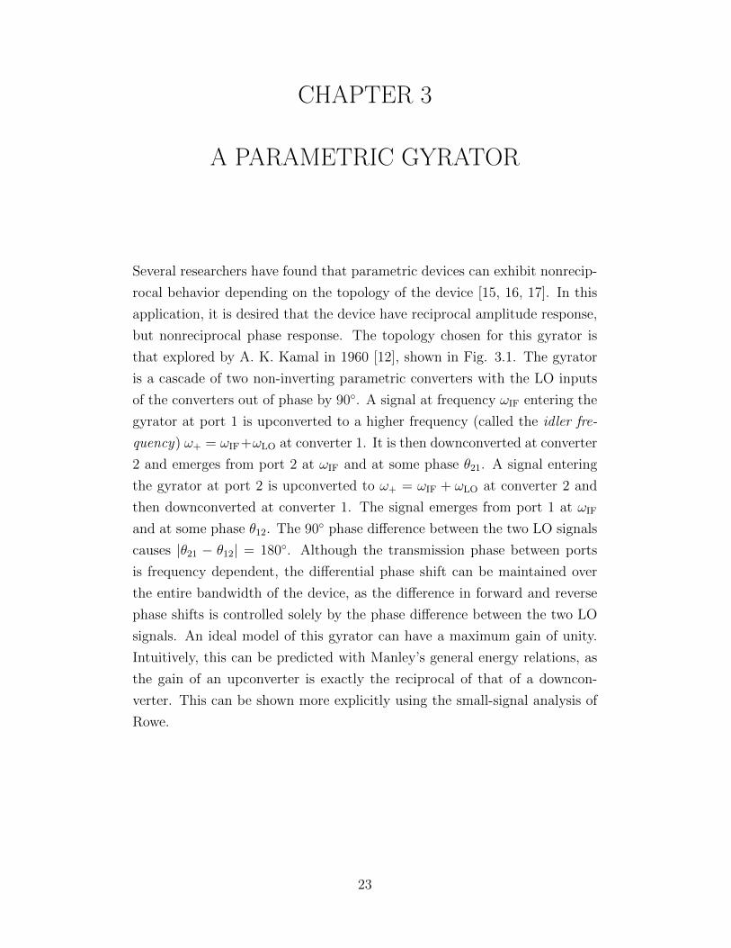
Several researchers have found that parametric devices can exhibit nonrecip-
rocal behavior depending on the topology of the device [15, 16, 17]. In this
application, it is desired that the device have reciprocal amplitude response,
but nonreciprocal phase response. The topology chosen for this gyrator is
that explored by A. K. Kamal in 1960 [12], shown in Fig. 3.1. The gyrator
is a cascade of two non-inverting parametric converters with the LO inputs
of the converters out of phase by 90. A signal at frequency ωIF entering the
gyrator at port 1 is upconverted to a higher frequency (called the idler fre-
quency) ω+ = ωIF+ωLO at converter 1. It is then downconverted at converter
2 and emerges from port 2 at ωIF and at some phase θ21. A signal entering
the gyrator at port 2 is upconverted to ω+ = ωIF + ωLO at converter 2 and
then downconverted at converter 1. The signal emerges from port 1 at ωIF
and at some phase θ12. The 90 phase difference between the two LO signals
causes |θ21 − θ12| = 180. Although the transmission phase between ports
is frequency dependent, the differential phase shift can be maintained over
the entire bandwidth of the device, as the difference in forward and reverse
phase shifts is controlled solely by the phase difference between the two LO
signals. An ideal model of this gyrator can have a maximum gain of unity.
Intuitively, this can be predicted with Manley’s general energy relations, as
the gain of an upconverter is exactly the reciprocal of that of a downcon-
verter. This can be shown more explicitly using the small-signal analysis of
Rowe.
23

Figure 3.1: Component-level diagram of parametric gyrator.
3.1 Theory of Operation
If the LO in a non-inverting converter is now allowed to have a phase angle
θ, then the time-varying capacitance in equation 2.23 can be expressed as
in equation 3.1, assuming the fundamental tone of the LO is the only signal
modulating the capacitor.
C(t) = C0 + 2C1 cos(2πfLO + θ) (3.1)
Considering equation 2.22, it is clear that θ can be considered the phase
angle of C1. Thus, the admittance matrix of equation 2.27 can be rewritten
as
[IIF
I+
]= j2π
(fIFC0 fIF|C1|ejθ
f+|C1|e−jθ f+C0
)[VIF
V+
](3.2)
The ABCD matrix formalism is more amenable to analysis of a cascade of
two-port networks, and so the matrix of equation 3.2 is expressed in ABCD
form as
[VIF
IIF
]=
(e−jθ 0
0 e−jθ
)(− C0
|C1|j
ωIF|C1|
jωIF(|C1| − C20
|C1|) −ωIF
ω+
C0
|C1|
)[V+
I+
](3.3)
In equation 3.3, this represents an upconverter. A downconverter would have
24

a matrix equal to the inverse of this matrix, or:
[V+
I+
]=
(ejθ 0
0 ejθ
)(− C0
|C1|j
ωIF|C1|
jωIF(|C1| − C20
|C1|) −ωIF
ω+
C0
|C1|
)−1 [VIF
IIF
](3.4)
Now, the overall ABCD matrix of the gyrator can be found by taking the
product of each of the ABCD matrices of each converter in Fig. 3.1:
[V1
I1
]=
(e−jα 0
0 e−jα
)(− C0
|C1|j
ωIF|C1|
jωIF(|C1| − C20
|C1|) −ωIF
ω+
C0
|C1|
)×
(ejβ 0
0 ejβ
)(− C0
|C1|j
ωIF|C1|
jωIF(|C1| − C20
|C1|) −ωIF
ω+
C0
|C1|
)−1 [V2
I2
]
=
(ej(β−α) 0
0 ej(β−α)
)[V2
I2
](3.5)
The nonreciprocity of the device can be seen more clearly by converting the
ABCD matrix to a scattering matrix:
[S] =
(0 ej(β−α)
ej(α−β) 0
)(3.6)
If α = 0 and β = π2, then the scattering matrix becomes
[S] = j
(0 1
−1 0
)(3.7)
This is the function of a gyrator, except there is an additional π2
phase delay
in each direction, but the differential phase shift is π. In practice, there will
be additional phase delay in each direction because of filter networks, tuning
elements, etc. but the differential phase is controlled solely by the phase
difference of the two LO signals.
25

3.2 Amplitude Response
When constructing parametric devices, the nonlinear reactance utilized will
have some appreciable loss. Assuming the device is constructed using loss-
less filters, the effect of nonideal reactance on various performance parame-
ters can be estimated. Including the losses in filters and matching elements
can be used to model the loss even more accurately if those losses are non-
negligible.
3.2.1 Insertion Loss
Insertion loss (IL) of a two-port device is defined as the ratio of output
power observed at a port to the input power supplied to the other port, and
is expressed in decibel scale. If a two-port network has some transducer gain
function GT , under the condition of conjugate matching at both ports, the
transducer gain becomes equal to the available gain, GA. For a cascade of
two-ports each conjugately matched at each port, the total gain of the system
is the product of each two-port’s available gain. In other words, if there are
n two-ports, each with available gain GA,n, then the overall available gain
GA,network of the network is
GA,network =n∏i=1
GA,n (3.8)
This fact is useful, as the insertion loss of the gyrator can be estimated
by deriving the transducer gain of an individual conjugately matched con-
verter, and then taking the product of the transducer gains of two converters.
Whether a signal propagates from port 1 to port 2 or vice versa, it will en-
counter an upconversion stage and then a downconversion stage (although it
is possible to design the converter to begin with a downconversion stage and
end with an upconversion stage). Therefore, the transducer gains of an up-
converter and a downconverter should be explored. Varactors are frequently
used in parametric converters, and the loss in a varactor is characterized
using a series resistance. It is more convenient, then, to work in terms of
the impedance matrix of a non-inverting parametric converter. First, the
26

time-varying capacitance is re-expressed as
C(t) = C0(1 + 2ψ cos(ωLOt+ θ)) (3.9)
where ψ is the modulation parameter, and is restricted to be 0 < ψ < 12
so
C(t) is positive. The impedance matrix can then be found by inverting the
admittance matrix of equation 2.27 after replacing C1 with ψC0ejθ:
[VIF
V+
]=
(1
jωIFC0(1−ψ2)ψ
jω+C0(1−ψ2)ejθ
ψjωIFC0(1−ψ2)
e−jθ 1jω+C0(1−ψ2)
)[IIF
I+
](3.10)
This impedance matrix can be used in the Thevenin equivalent circuit of the
parametric converter, shown in Fig. 3.2. The impedance matrix of equation
3.10 represents the two-port network labeled “Nonlinear Capacitor”.
Figure 3.2: Thevenin equivalent circuit of non-inverting parametricconverter. The nonlinear capacitor can be represented by the impedancematrix of equation 3.10.
RS and RL represent the source and load impedances, respectively. XS and
XL are the tuning reactances at the source and load, respectively. Filters at
the input and output ensure the assumption that only fIF is present at the
input and f+ is present at the output. The loss of the nonlinear capacitor is
modeled as a series resistance Rc. To simplify the derivation, it is assumed
that the source and load impedances are equal (RS = RL = R) and purely
resistive. The input impedance presented to the source, Zin, can be expressed
as
27

Zin = Rc + j
(XS −
1
ωIFC0(1− ψ2)
)+
1
ωIFω+
(ψ
C0(1− ψ2)
)2
× 1
j
(XS − 1
ω+C0(1−ψ2)
)+R
(3.11)
To match the converter at both ports, XS and XL should be positive reac-
tances, and so inductors are selected. The reactances can then be written as
XS = ωIFLS and XL = ω+LL, where LS and LL are the source and load tun-
ing inductances, respectively. These inductances are chosen to tune out the
static portion of the capacitance, which allows a resistive input impedance
and output impedance to be presented to the source and load terminations,
respectively.
LS =1
ω2IFC0(1− γ2)
(3.12)
LL =1
ω2+C0(1− γ2)
(3.13)
Under this matching condition, the input impedance reduces to
Zin = Rc +1
ωIFω+
(ψ
C0(1− ψ2)
)2(1
R +Rc
)(3.14)
The transducer gain under the matching condition can be expressed as
GT =4|Z21|2R2
|ZinZout − Z12Z21|2
=4R2 ψ2
ω2IFC
20 (1−ψ2)2
(R2 +R2c + 2RRc + ψ2
ωIFω+C20 (1−ψ2)2
)2(3.15)
with Zout defined as
28
Zout = Rc +1
ωIFω+
(ψ
(C0(1− ψ2))
)2(1
R +Rc
)(3.16)
The symmetry of the equivalent circuit causes Zin = Zout, meaning both
ports can be conjugately matched. To find the optimum source and load
terminations, the derivative of the transducer gain is taken with respect to
R and then set to zero.
dGT
dR=
8 ψ2
ω2IFC
20 (1−ψ2)2
R( ψ2
ωIFω+C20 (1−ψ2)2
+R2c −R2)
( ψ2
ωIFω+C20 (1−ψ2)2
+ (Rc +R)2)3= 0 (3.17)
The value of R that satisfies this condition is given by
RS = RL = Rc
√1 +
ψ2
ωIFω+R2cC
20(1− ψ2)2
(3.18)
With this selection of R, at the center frequency of operation, Zin = Zout = R.
This is exactly the condition for conjugate matching at both ports. In order
to characterize the lossy behavior of a varactor, the dynamic quality factor,
Qd, is introduced:
Qd =1
ωIFRcC0(1− ψ2)(3.19)
Much like the ubiquitous figure of merit Q of an ordinary resonator, a large
value of Qd indicates a low-loss device. A device with Qd = ∞ is lossless,
and one would expect the transducer gain of such a device to be f+fIF
. Using
this new definition, GT as defined in equation 3.15 can be rewritten.
GT =(1 + ωIF
ω+ψ2Q2
d)Q2dψ
2
((1 + ωIF
ω+ψ2Q2
d) +√
1 + ωIF
ω+ψ2Q2
d)2(3.20)
Now, a new parameter, ξ, called the dynamic loss factor is defined:
ξ2 =f+fIF
1
(ψQd)2(3.21)
29

The transducer gain can then be rearranged to be in terms of this new pa-
rameter.
GT =ω+
ωIF
1
(ξ +√
1 + ξ2)2(3.22)
When ξ = 0, the transducer gain is f+fIF
for an upconverter and fIFf+
for a
downconverter, the result for a lossless parametric converter following the
formalism of Manley and Rowe (recall that an upconverter has an input
frequency fIF and an output frequency of f+, but a downconverter has the
opposite). This is also apparent because ξ = 0 when Qd =∞. Returning to
the discussion of the gyrator of Fig. 3.1, when both converters are conjugately
matched at both ports, each converter’s transducer gain GT becomes equal to
its available gain GA, and thus the insertion loss of the gyrator is the product
of the transducer gain of an upconversion stage, G↑, and the transducer gain
of a downconversion stage, G↓.
G↑ =ω+
ωIF
1
(ξ +√
1 + ξ2)2(3.23)
G↓ =ωIF
ω+
1
(ξ +√
1 + ξ2)2(3.24)
The insertion loss is then expressed as
IL = G↑G↓ =1
(ξ +√
1 + ξ2)4(3.25)
Although this analysis was performed assuming the initial stage of the
gyrator is an upconverter and the final stage is a downconverter, the results
are identical in the case that the first stage is an upconverter and the last
stage is a downconverter. This is because the product of transducer gains is
commutative, meaning G↑G↓ = G↓G↑. In Fig. 3.3, the insertion loss of the
gyrator is plotted over dynamic quality factor for various conversion ratios
( ω+
ωIF).
30
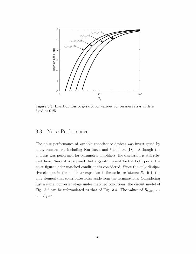
Figure 3.3: Insertion loss of gyrator for various conversion ratios with ψfixed at 0.25.
3.3 Noise Performance
The noise performance of variable capacitance devices was investigated by
many researchers, including Kurokawa and Uenohara [18]. Although the
analysis was performed for parametric amplifiers, the discussion is still rele-
vant here. Since it is required that a gyrator is matched at both ports, the
noise figure under matched conditions is considered. Since the only dissipa-
tive element in the nonlinear capacitor is the series resistance Rc, it is the
only element that contributes noise aside from the terminations. Considering
just a signal converter stage under matched conditions, the circuit model of
Fig. 3.2 can be reformulated as that of Fig. 3.4. The values of RCAP, A↑
and A↓ are
31

Figure 3.4: Equivalent noise model of both upconverter and downconverter.
RCAP =ψ2
(R +Rc)ωIFω+C20(1− ψ2)2
(3.26a)
|A↑|2 =ω+
ωIF
1
(ξ +√
1 + ξ2)2(3.26b)
|A↓|2 =ωIF
ω+
1
(ξ +√
1 + ξ2)2(3.26c)
The noise factor (F ) is then defined as the ratio of the SNR across the
input resistance to the SNR across the output resistance. As in Fig. 3.4,
the upconverter and downconverter are considered as separate cases, as the
roles of the terminations as input and output are different in these cases. In
general, the noise factor can be expressed as in equation 3.27 where Ps,IN is
the input signal power, Ps,OUT is the output signal power, PN,OUT is the noise
output power and PN,IN is the noise input power.
32
F =SNRIN
SNROUT
=Ps,INPs,OUT
× PN,OUT
PN,IN(3.27)
3.3.1 Parametric Modulator Noise Factor
In reference to Fig. 3.4, the noise factor can be found for an upconverter by
taking 3.27 and rewriting it as
F↑ =1
|A↑|2× PN,OUT
PN,IN(3.28)
Since the ratio of the output to input noise power is needed, finding the
square RMS noise voltage at both the input and output is sufficient to com-
pute this ratio. The square RMS noise voltage at the input, v2N,in,RMS, is the
familiar quantity 4kTBRs, where k is Boltzmann’s constant, T is the phys-
ical temperature and B is the measurement bandwidth. The square RMS
output noise voltage, v2N,out,RMS, at the output can then be found from the
upconverter model.
v2N,out,RMS = 4kTB
(Rc +RL + |A↑|2(Rs +Rc)
)(3.29)
Applying the matching condition of 3.18, this can be further simplified:
v2N,out,RMS = 4kTBRc
(1 +
√1 +
1
ξ2
)(1 + |A↑|2
)(3.30)
Now, the noise factor, F↑, can be found from these quantities:
F↑ =1
|A↑|2×v2N,out,RMS
v2N,in,RMS
= 1 +ξ√
1 + ξ2+ωIF
ω+
(1 +
ξ√1 + ξ2
)(ξ +
√1 + ξ2
)2
(3.31)
For a downconverter, the same procedure can be utilized to find the noise
33

factor, F↓:
F↓ = 1 +ξ√
1 + ξ2+ω+
ωIF
(1 +
ξ√1 + ξ2
)(ξ +
√1 + ξ2
)2
(3.32)
If the modulation parameter ψ is held fixed, a lower noise factor is achieved
using a higher LO frequency (as ω+ = ωIF + ωLO) for an upconverter, but
this is the opposite for a downconverter. This is evident in Fig. 3.5. If the
LO frequency is fixed, then a deeper modulation depth (larger value of ψ)
can achieve a somewhat lower noise factor. This is demonstrated in Fig. 3.6
for both an upconverter and downconverter.
3.3.2 Gyrator Noise Factor
Since the upconverter has a lower noise factor and provides gain, it is fairly
obvious that a gyrator whose first stage is an upconverter and second stage is
a downconverter yields the lowest noise factor. For that reason, only this case
is investigated. It is trivial to find this noise factor, Fgyrator, using the Friis
formula of equation 1.25. The expression is more convenient when written
in terms of the insertion loss (IL) defined in equation 3.25:
Fgyrator = F↑ +F↓ − 1
|A↑|2
=ωIF
ω+
1√IL
+ 2
[1 +
ξ√1 + ξ2
(1 +
ωIF
ω+
1√IL
)](3.33)
In the losssless case, ξ = 0 and IL = 1, which reduces the gyrator noise
factor to 2 + ωIF
ω+. As a brief example, for conversion ratios ( ω+
ωIF) of 1.5, 3 and
5, the noise figures would be 4.26 dB, 3.68 dB and 3.42 dB, respectively. Of
course, this derivation assumes the only contributor to noise by the nonlinear
capacitor itself is the series loss resistance Rc, but nonlinear capacitors are
often implemented using varactor diodes. In this case, other factors such as
shot noise would need to be considered. In a design situation, typically the
34

Figure 3.5: Noise figure for a fixed modulation parameter (ψ = 0.25) for anupconverter (F↑) and a downconverter (F↓).
35

Figure 3.6: Noise figure for a fixed frequency ratio ( ω+
ωIF= 3) for an
upconverter (F↑) and a downconverter (F↓).
36
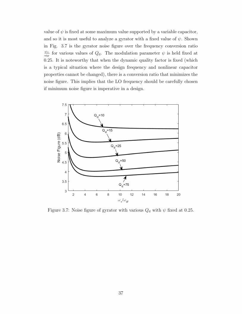
value of ψ is fixed at some maximum value supported by a variable capacitor,
and so it is most useful to analyze a gyrator with a fixed value of ψ. Shown
in Fig. 3.7 is the gyrator noise figure over the frequency conversion ratioω+
ωIFfor various values of Qd. The modulation parameter ψ is held fixed at
0.25. It is noteworthy that when the dynamic quality factor is fixed (which
is a typical situation where the design frequency and nonlinear capacitor
properties cannot be changed), there is a conversion ratio that minimizes the
noise figure. This implies that the LO frequency should be carefully chosen
if minimum noise figure is imperative in a design.
Figure 3.7: Noise figure of gyrator with various Qd with ψ fixed at 0.25.
37

CHAPTER 4
ANALYSIS OF A FOUR-PORTPARAMETRIC GYRATOR-CIRCULATOR
As was discussed and shown in Fig. 1.4, circulators can be constructed
from gyrators, but the topologies shown only function properly for the ideal
circulator. When physically realized, the topologies must be adjusted to be
compatible with the nonidealities of the device. In both of the topologies,
circulation is achieved between port pairs by evenly dividing a signal incident
upon some port into two paths with one path having reciprocal phase and
another path having nonreciprocal phase. When the signal recombines at
the other port, it is combined either in phase or out of phase depending on
the direction of transmission. This mechanism requires that both paths have
the same time delay in order for the split signal to combine properly. This
is easily achieved in the topology of Fig. 1.4 (c) due to the symmetry of the
topology, but it is not so readily achieved in Fig. 1.4 (b). For this reason,
this section focuses primarily on the topology of Fig. 1.4 (c). It is of interest
to develop a method to estimate the time delay of the gyrator in order to
compensate for the effect. In addition, this circulator is bandwidth limited,
as the 180 phase balance between coupled ports in the hybrid coupler is
only maintained at the center frequency. The hybrid couplers only maintain
equal power division between coupled ports over a limited range as well. The
gyrator itself may limit the useful isolation bandwidth of the circulator if its
own amplitude bandwidth is limited. In the work of Manley and Rowe, it was
found that having a high conversion ratio ω+
ωIFcan yield a higher amplitude
bandwidth, and the noise analysis of the previous chapter found that in
general, up to a certain point, higher conversion ratios yield a lower noise
figure.
38

4.1 Theory of Operation
As stated before, the parametric gyrator relies on cancellation of signals to
achieve isolation at various ports. There are essentially two elements that
comprise the four-port circulator. The first element is a passive, recriprocal
power divider/combiner known as a 180 hybrid coupler. The other is the
nonreciprocal component, which is the parametric gyrator.
4.1.1 The 180 Hybrid Coupler
The 180 hybrid coupler, henceforth referred to as a hybrid for brevity, is
a common component in microwave engineering. It is a four-port passive
device that can be realized in many forms, such as a waveguide magic tee
or a microstrip ratrace coupler. Although various properties of the hybrid
(such as bandwidth) are dependent its realization, the function is the same
irrespective of implementation. The ideal scattering matrix of the hybrid at
its center frequency is
S =−j√
2
0 1 1 0
1 0 0 −1
1 0 0 1
0 −1 1 0
(4.1)
For any given port, the remaining three ports are termed the sum port
(represented with the symbol Σ), the difference port (represented with the
symbol ∆) and the isolated port. When a signal is sent through a port,
the hybrid divides it equally between the sum and difference ports. The
divided signals are in phase with each other. The isolated port ideally has
no signal exit. For example, if a signal is sent into port 1 of the hybrid, port
2 is the sum port, port 3 is the difference port and port 4 is the isolated
port. Alternatively, the hybrid can operate as a combiner. Now, if a signal is
applied to both the input port and isolated port, the sum port outputs the
sum of the two signals and the difference port outputs the difference of the
two signals. Using the same example as before, if two equal power, in-phase
signals are applied to ports 1 and 4 each, then port 2 outputs the sum of the
39

two signals and port 3 should output no signal, since the difference between
the two signals is zero. Figure 4.1 shows the system-level symbol commonly
used for a hybrid, as well as a pictorial representation of the magic tee and
the microstrip ratrace hybrid. In Kamal’s work, the hybrid of choice was the
magic tee, as parametric modulators were often constructed in waveguide
form at the time.
Figure 4.1: (a) System level diagram of hybrid coupler. (b) Waveguidemagic tee. (c) Microstrip ratrace coupler.
4.1.2 Operation of Right-Handed Four-Port Circulator
The operation of the four-port circulator is shown pictorially in Fig. 4.2.
In the diagram, the gyrator is represented as a box with its ideal scattering
matrix. Port 1 is on the lefthand side and port 2 is on the righthand side.
40

Figure 4.2: Graphical representation of operation of right-handed four-portparametric circulator. All quantities shown are in phasor form.
41

Consider a time-harmonic signal incident upon port 1 of the form V1(t) =
V cos(ωt). In phasor form, this is represented as V1 = V ej0. The lefthand
hybrid (lh) evenly divides this signal between two paths: one with the gyrator
and the other a short. The signal leaving the hybrid on both paths can be
written in phasor form as V√2e−j90
. The gyrator imparts a 180 phase delay
on the signal passing through its path and the signal on the other path
is unchanged. The righthand hybrid (rh) then acts as a combiner for two
signals, one coming from the gyrator with the form V√2e−j270
and one from
the short of the form V√2e−j90
. Port 4 of the circulator then becomes the
righthand hybrid’s sum port, and the output is then V4(t) = 0. Port 2 of the
circulator becomes the righthand hybrid’s difference port, and the output
from this port is then V2(t) = −V cos(ωt). From this, one can infer that
S21 = −j and S31 = S41 = 0. One can infer the remaining S-parameters
through a similar approach keeping in mind that the gyrator imparts a 180
phase shift to a signal traveling from the lefthand hybrid to the righthand
hybrid, but imparts no phase shift to a signal traveling from the righthand
hybrid to the lefthand hybrid. Since both hybrids are matched at all four
ports and the gyrator is matched at all four ports, all four ports of the
circulator will be matched as well. The four-port circulator therefore has the
scattering matrix
S = −j
0 0 0 1
1 0 0 0
0 1 0 0
0 0 1 0
(4.2)
This is almost the ideal scattering matrix of equation 1.19 except there
is an additional 90 phase shift imparted on a circulated signal. It is also
worth noting that instead of 180 hybrids, a designer can also use four-port
quadrature couplers (such as a branchline coupler) to achieve the four-port
circulator. As an exercise to the reader, it may be shown that the matrix of
equation 4.2 would become
42

S =
0 0 0 1
j 0 0 0
0 −1 0 0
0 0 j 0
(4.3)
4.1.3 Reversal of Rotation Sense
One important property of the parametric gyrator is its ability to reverse its
values of S21 and S12 by changing the LO phase. Recall that the choice of
α = 0 and β = π2
in equation 3.6 yielded the scattering matrix of 3.7. By
now choosing α = π2
and β = 0, the scattering matrix of equation 3.6 changes
to
S = j
(0 1
−1 0
)(4.4)
A simple analysis similar to that of the previous section can be used to show
that the scattering matrix becomes
S = −j
0 1 0 0
0 0 1 0
0 0 0 1
1 0 0 0
(4.5)
A pictorial representation of the left-handed version of the four-port cir-
culator is shown in Fig. 4.3. Note the only change to the topology was
reversing the phase shifting direction of the gyrator. In practice, this can be
accomplished trivially by using switched delay lines or phase shifters for the
LO signal.
43

Figure 4.3: Graphical representation of operation of left-handed four-portparametric circulator.
44
4.2 Transmission Phase and Group Delay of
Parametric Gyrator
As mentioned in the introduction to this chapter, the physical realization of
the gyrator-circulator requires knowledge of the transmission properties of
the gyrator. Although the amplitude response was explored in chapter 3,
the phase response is also of interest. Since the ideal gyrator transmission
phase must be equal to 2nπ in one direction and (2n + 1)π in the other for
n ∈ R, it is important to be able to predict this phase in case it needs to
be adjusted to satisfy these conditions. In addition, in order for the delay
of the two paths connecting the hybrids in the four-port topology to be the
same, it is imperative that the group delay of the gyrator be estimated as
well.
4.2.1 Derivation
The impedance matrix of equation 3.10 can be utilized to predict the phase
imparted by a nonlinear capacitor. The voltage gain of a two-port network
with respect to its impedance parameters is
Av =Z21ZL
(Z11 + ZG)(Z22 + ZL)− Z12Z21
(4.6)
The phase of this quantity is readily found from its real and imaginary
parts.
∠Av = arctan
(=(Av)
<(Av)
)(4.7)
∠Av can be interpreted as the phase of the signal exiting the nonlinear capac-
itor. In the previous sections, it was implicitly assumed that filters enforced
a single frequency component at each port of the parametric modulators used
to construct the gyrator. To accurately model the transmission phase, the
filters must now be accounted for. The filters tuned to ωIF are assumed to
impart a phase delay of θIF(ω) within their passbands. The filter tuned to ω+
is assumed to impart a phase delay of θ+(ω+ωLO) in its passband. Denoting
45

the transmission phase from port 1 to port 2 as θ21(ω) and that from port
2 to port 1 as θ12(ω), a new equivalent model of the gyrator is given in Fig.
4.4.
Figure 4.4: Expanded model of parametric gyrator that explicitly accountsfor the effects of the necessary filters. The components ZL and ZR can bothbe described by the matrix of 3.10 by substituting the value of θ with αand β, respectively. As before, these quantities denote the LO phase.
Ignoring the effect of the loss resistance Rc in the modulators, the relevant
voltage gain quantities can be computed:
AL21 = e−jαAv↑(ω) (4.8a)
AL12 = ejαAv↓(ω) (4.8b)
AR21 = e−jβAv↓(ω) (4.8c)
AR12 = ejβAv↑(ω) (4.8d)
The other quantities can be found from:
46
Av↑(ω) =j ψωIFC0(1−ψ2)
R
ZINZOUT + ψ2
ωIFω+C20 (1−ψ2)2
(4.9a)
Av↓(ω) =j ψω+C0(1−ψ2)
R
ZINZOUT + ψ2
ωIFω+C20 (1−ψ2)2
(4.9b)
ZIN = j
(ωIFLS −
1
ωIFC0(1− ψ2)
)+R (4.9c)
ZOUT = j
(ω+LL −
1
ω+C0(1− ψ2)
)+R (4.9d)
R =ψ
√ωIFω+C0(1− ψ2)
(4.9e)
The inductor values LS and LL are given by equations 3.12 and 3.13, respec-
tively. Finally, the transmission phase in each direction is given by equation
4.10. For the gyrator, as before, one should select α = 0 and β = 90 or
α = 90 and β = 0.
θ21(ω) = 2θIF(ω) + ∠AL21(ω) + θ+(ω + ωLO) + ∠AR21(ω) (4.10a)
θ12(ω) = 2θIF(ω) + ∠AL12(ω) + θ+(ω + ωLO) + ∠AR12(ω) (4.10b)
The group delay from port 1 to port 2, τg21, and that from port 2 to port 1,
τg12, can be found from
τg21 = − d
dωθ21(ω) (4.11a)
τg12 = − d
dωθ12(ω) (4.11b)
It is desirable for the gyrator to add no distortion to signals passing through
it, which means τg21 = τg12 = const. over frequency. This is achieved when
θ21 and θ12 are linear over frequency and have the same slope.
47
4.2.2 Design Examples
Two design examples are given here to demonstrate the use of this approach.
In the first example, the method is used at the center frequency to determine
the additional phase delay that must be added to the gyrator in order for its
behavior to approach ideal. In the second example, the group delay of an
idealized gyrator is estimated.
4.2.2.1 Example 1 - Center Frequency Transmission Phase
fIF = 500 MHz
fLO = 1000 MHz
C0 = 1 pF
ψ = 0.3
θIF = −100 at 500 MHz
θ+ = −150 at 1500 MHz
Assuming the lefthand modulator has a LO phase of 0 and the righthand
modulator has a LO phase of 90, the analysis starts from equations 3.12
and 3.13 to find that LS = 111.3 nH and LL = 12.4 nH. From equation
4.9e, R = 60.6Ω. These quantities can be used to find that AL21 = AL12 =
−90, AR12 = 0 and AR12 = −180. Thus, θ21 = −620 and θ12 = −440.
Therefore, an extra -100 of phase delay should be added to the gyrator for
its S-matrix to become that of equation 4.12 at ω = ωIF, which is the ideal
gyrator.
S =
(0 −1
1 0
)(4.12)
4.2.2.2 Example 2 - Group Delay
fIF = 500 MHz
48

fLO = 1000 MHz
C0 = 1 pF
ψ = 0.3
θIF = 0
θ+ = 0
The filters are assumed to be phaseless, since any number of filters can be
chosen in the event the nonlinear capacitors have undesirable phase charac-
teristics. The values of LL, LS and R are the same as in Example 1. First,
the value of θ21(ω) can be evaluated. The values of ∠AL21, ∠AL12, ∠AR21,
and ∠AR12 are computed and shown in Fig. 4.5 along with the transducer
gain normalized to the ideal Manley-Rowe value. The frequency range cor-
responds to the 3 dB bandwidth of 402 - 588 MHz, or 37.2%. Now, the two
phase curves can be added together to find the overall transmission phase.
This exercise can be repeated for θ21(ω) as well. Shown in Fig. 4.6 is the
transmission phase in both directions of the gyrator. Note that the addition
of filters can serve to change the shape of the phase plot if different character-
istics are required. Mathematically, this confirms the derivation of equation
3.7, as in Fig. 4.6, it is seen that the values of the transmission phase at the
center frequency, 500 MHz, are exactly as predicted by 3.7. Now, the group
delay is found by taking the derivative of each phase curve with respect to
frequency. The phase slope is found to be 0.8801 /MHz through a line of
best fit (R2 = 0.9987), meaning the group delay is 2.44 ns. If more realis-
tic filters were included, the total group delay of the gyrator would be this
calculated value plus the group delay of each individual filter.
4.3 Adjusted Circulator Topologies
Shown in Fig. 4.7 are two topologies that can be used to physically realize the
gyrator-circulator. Figure 4.7a shows the familiar four-port circulator. Two
new elements have been added: a delay balancer and a phase compensator.
The phase compensation is used to ensure the gyrator provides a 2nπ phase
49

Figure 4.5: Computed values of ∠AL21, ∠AL12, ∠AR21, and ∠AR12
alongside modulator/demodulator transducer gain. The gain is normalizedto the ideal Manley-Rowe value: fp+f
ffor an upconverter and f
f+fpfor a
downconverter.
Figure 4.6: Transmission phase characteristic in each direction over the 3dB bandwidth of the gyrator.
50

Figure 4.7: (a) Adjusted four-port circulator topology and (b)approximation of three-port circulator. The phase compensation can beused to tune the center frequency of the gyrator to the center frequency ofthe hybrids and dividers. The delay balance has a time delay equal to thecombined delay of the gyrator and the phase compensation.
51
shift in one direction and a (2n + 1)π phase shift in the other at the center
frequency of operation. This is necessary to ensure the gyrator operates
at the same center frequency of the two hybrids in order to ensure proper
operation. In the arm below the gyrator, the delay balancer is adjusted to
provide a path delay equal to the delay of both the gyrator and the phase
compensator. Its group delay should be the same as in expression 4.11.
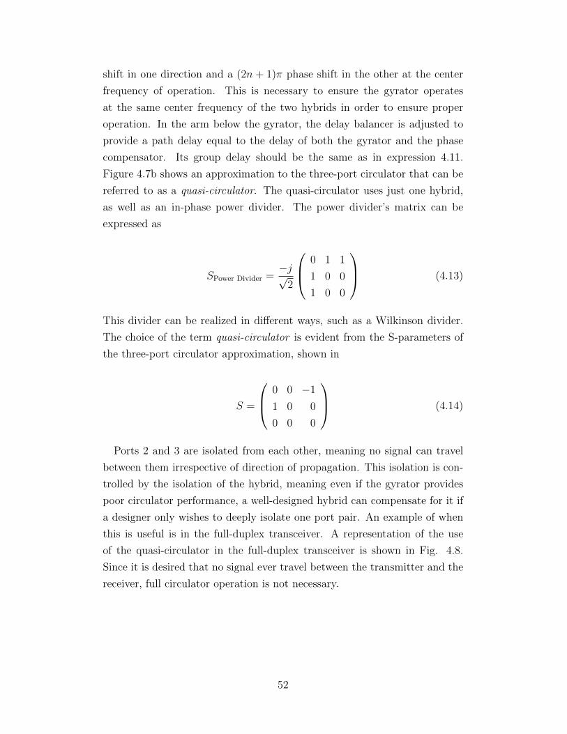
Figure 4.7b shows an approximation to the three-port circulator that can be
referred to as a quasi-circulator. The quasi-circulator uses just one hybrid,
as well as an in-phase power divider. The power divider’s matrix can be
expressed as
SPower Divider =−j√
2
0 1 1
1 0 0
1 0 0
(4.13)
This divider can be realized in different ways, such as a Wilkinson divider.
The choice of the term quasi-circulator is evident from the S-parameters of
the three-port circulator approximation, shown in
S =
0 0 −1
1 0 0
0 0 0
(4.14)
Ports 2 and 3 are isolated from each other, meaning no signal can travel
between them irrespective of direction of propagation. This isolation is con-
trolled by the isolation of the hybrid, meaning even if the gyrator provides
poor circulator performance, a well-designed hybrid can compensate for it if
a designer only wishes to deeply isolate one port pair. An example of when
this is useful is in the full-duplex transceiver. A representation of the use
of the quasi-circulator in the full-duplex transceiver is shown in Fig. 4.8.
Since it is desired that no signal ever travel between the transmitter and the
receiver, full circulator operation is not necessary.
52
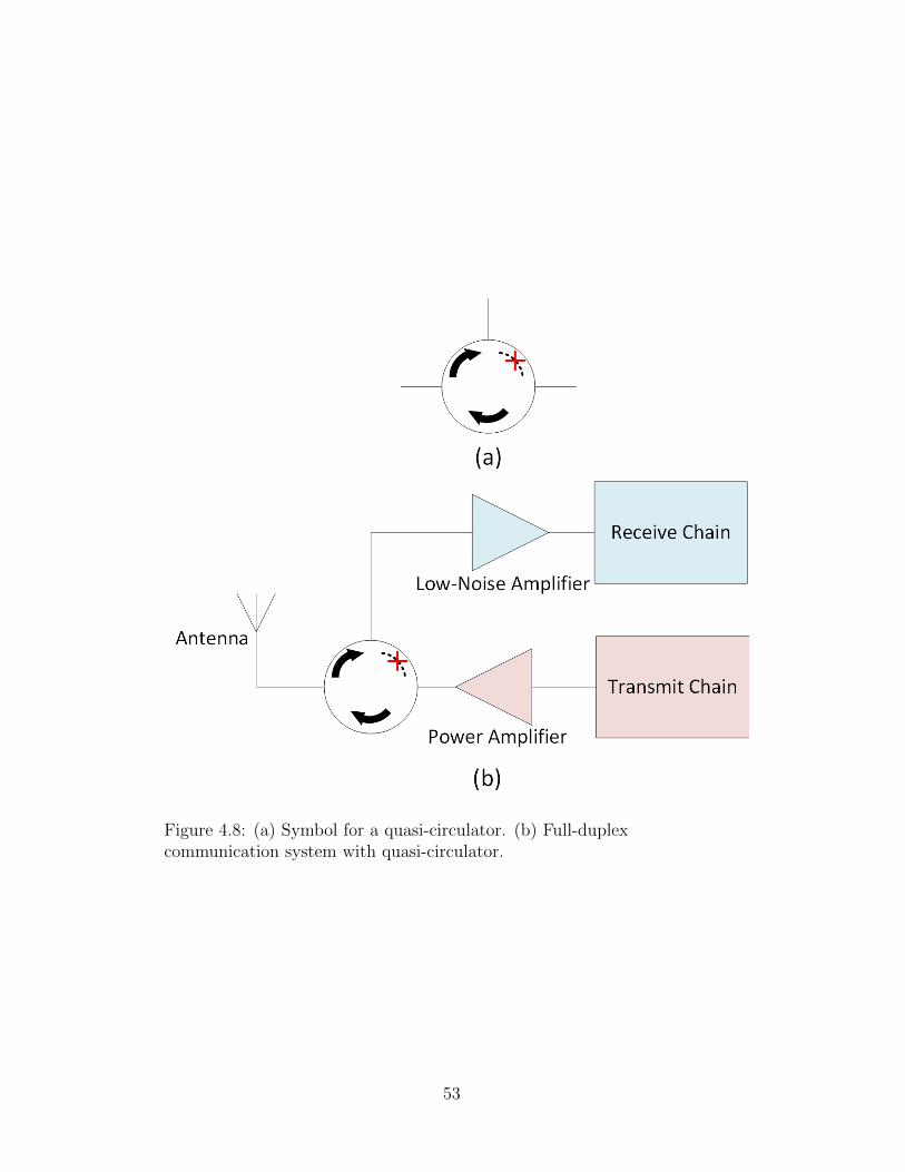
Figure 4.8: (a) Symbol for a quasi-circulator. (b) Full-duplexcommunication system with quasi-circulator.
53

4.4 Bandwidth Performance
The circulator isolation bandwidth is controlled by both the bandwidths of
the hybrids as well as the amplitude bandwidth of the gyrator. Even if the
gyrator’s bandwidth is quite broad, the hybrids have limitations based on
their topology. It is of interest, then, to investigate the upper limits on
bandwidth due to the hybrids themselves.
4.4.1 Ideal Four-Port Gyrator-Circulator IsolationPerformance
S-parameter simulations were performed to estimate the maximum achievable
bandwidth of the gyrator-circulator using ideal, lossless transmission lines to
create various hybrid coupler topologies. The gyrator was modeled as a two-
port network with its S-parameters being that of 1.22 over all frequencies.
Since this circulator is ideal, it provides infinite isolation at the center of its
band, but this isolation rolls off with frequency. The isolation bandwidth of
the gyrator-circulator is defined to be the fractional bandwidth over which
the circulator provides at least 20 dB of isolation.
4.4.1.1 Ratrace Hybrid
The ratrace coupler, a 180 hybrid shown in Fig. 4.1, provides a maximum
achievable isolation bandwidth of 17.1%, as seen in Fig. 4.9.
54

Figure 4.9: Isolation performance of idealized four-port circulator usingratrace hybrids. The isolation characteristic is not identical between allport pairs.
4.4.1.2 Branchline Hybrid
The branchline coupler is a quadrature coupler shown schematically in Fig.
4.10. Since it is also a four-port device like the 180 hybrid, it is connected in
the same fashion as the 180 hybrid in the topologies of 4.7. Observing the
S-parameter simulation in Fig. 4.11, it displays even less symmetry than the
ratrace hybrid, but the bandwidth of the narrower curve is 17.6%, which is
more or less the same as the circulator constructed with ratrace hybrids.
55

Figure 4.10: Transmission line realization of branchline coupler. All linesare 90 in electrical length.
Figure 4.11: Isolation performance of idealized four-port circulator usingbranchline hybrids. The isolation characteristic is not identical between allport pairs.
4.4.2 Broadband Realization of the Gyrator-Circulator
In order to create a broadband architecture for the gyrator-circulator, a de-
signer must broaden the bandwidths of both the hybrids and the gyrator it-
self. Although there are many topologies of hybrids that can achieve this, this
section focuses on the multistage branchline hybrid as an example. Although
there have been several efforts in broadbanding the branchline coupler, one
simple topology called the double-box branchline [19] can be employed here.
A schematic representation of the idealized gyrator-circulator with with the
double-box hybrids is shown in Fig. 4.12. S-parameter simulations, shown
56
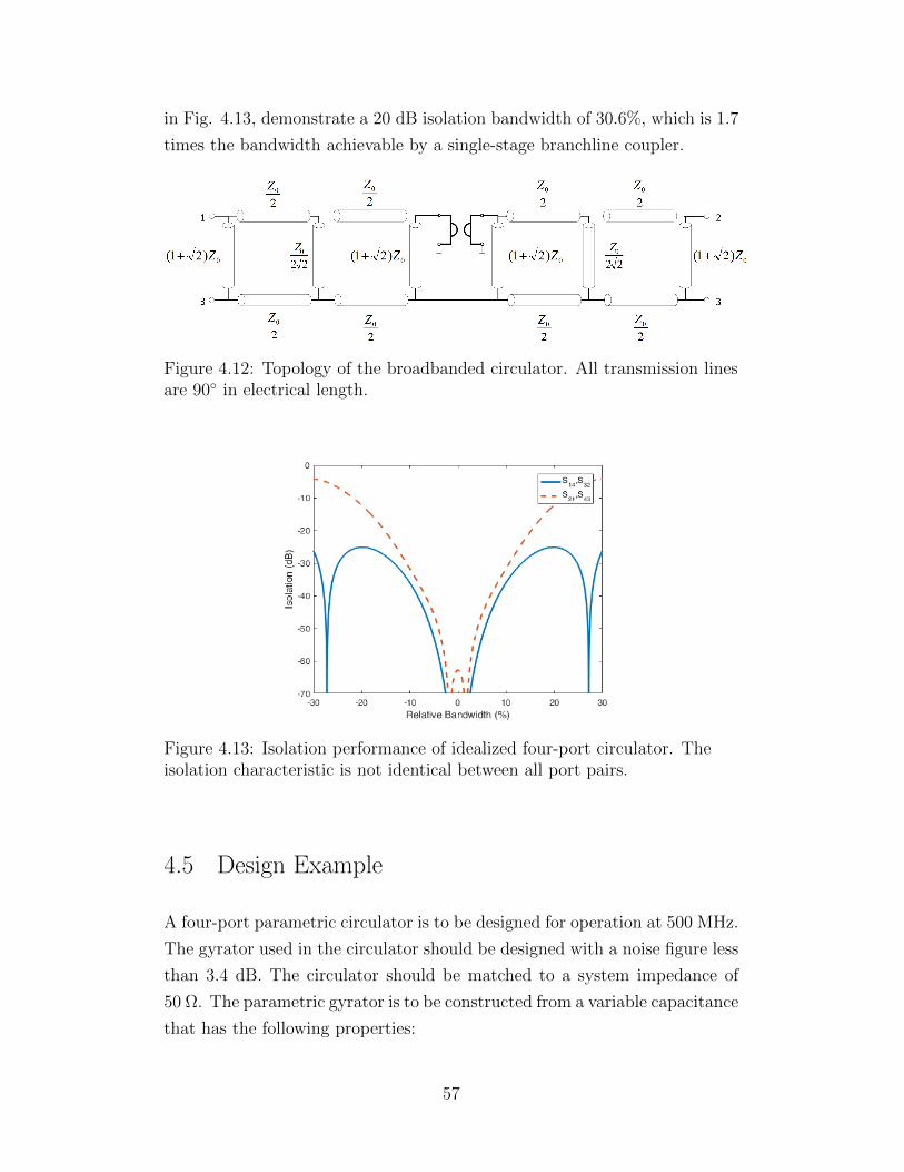
in Fig. 4.13, demonstrate a 20 dB isolation bandwidth of 30.6%, which is 1.7
times the bandwidth achievable by a single-stage branchline coupler.
Figure 4.12: Topology of the broadbanded circulator. All transmission linesare 90 in electrical length.
Figure 4.13: Isolation performance of idealized four-port circulator. Theisolation characteristic is not identical between all port pairs.
4.5 Design Example
A four-port parametric circulator is to be designed for operation at 500 MHz.
The gyrator used in the circulator should be designed with a noise figure less
than 3.4 dB. The circulator should be matched to a system impedance of
50 Ω. The parametric gyrator is to be constructed from a variable capacitance
that has the following properties:
57

C0 = 1 pF
ψ = 0− 0.45
Rc = 2.5 Ω
The design begins by selecting an appropriate LO frequency ωLO and mod-
ulation parameter ψ. Since a large modulation parameter yields a lower noise
factor, the highest possible modulation parameter (ψ = 0.45) is used to find
the lowest possible LO frequency. Using equation 3.33, the noise figure can
be plotted for various LO frequencies as in Fig. 4.14.
Figure 4.14: Noise figure of the gyrator for various LO frequencies. Thedynamic quality factor Qd is approximately 160 for the highest supportedmodulation parameter.
Choosing fLO to be 2 GHz gives a slight margin below 3.4 dB noise figure.
Now, the actual modulation parameter can be selected. Since Rc = 2.5 Ω
and ωLO = 2π × 2 GHz, equation 3.18 can be used to find that ψ must be
0.41 to match to 50 Ω. This is close to the maximum modulation parameter,
and thus yields an actual noise figure of the gyrator still in the vicinity of 3.4
dB. From equations 3.12 and 3.13, the tuning inductances are LS = 152.3
nH and LL = 6.1 nH. From equation 3.19, Qd = 153 and from equation 3.21,
58

ξ2 = 0.00127. Finally, from equation 3.25, the predicted insertion loss of
the gyrator is 0.61 dB. Before simulating the gyrator, a simple S-parameter
simulation using ratrace couplers created with ideal transmission lines can
be used to predict the isolation at the center frequency for varying levels
of gyrator insertion loss. Observing such a simulation in Fig. 4.15, it can
be estimated that this gyrator in a four-port circulator with ideal ratrace
couplers will provide a center frequency isolation of 29.4 dB.
Figure 4.15: Four-port circulator insertion loss and isolation between portpairs for increasing levels of gyrator insertion loss.
The gyrator was then simulated using a harmonic balance routine. The
three filters used were Bessel-Thompson filters, chosen because of their highly
linear phase response. The two ωIF filters had a center frequency of 500 MHz
with 10% fractional bandwidth. The ω+ filter had a center frequency of
2500 MHz with a bandwidth of 10%, though a narrower bandwidth could
have been tolerated. The simulation was performed in Keysight ADS using
the schematic shown in Fig. 4.16. The tuning inductances were adjusted
slightly, as the filters provide some reactance even at the center frequency
that changes the tuning requirements.
59

Figure 4.16: Keysight ADS simulation of gyrator. LSSP simulationperforms the function of a typical harmonic balance simulation, but makescomputation of quantities like insertion loss and transducer gain simpler,especially when the frequency is swept over some range.
After setting up the simulation, the modulation parameter was swept over
the supported range of the nonlinear capacitor. As seen in Fig. 4.17, the
optimal value of ψ was in the vicinity of the predicted value of 0.41. The
insertion loss for this was slightly better than predicted, at about 0.55 dB.
With the gyrator optimized, a simulation was performed over frequency as
shown in Fig. 4.18. It can be seen that the gyrator’s amplitude response is
centered about 504 MHz with a 3 dB bandwidth of 6.3%. The phase of S21
and S12 at 500 MHz is -348 and -528, respectively, meaning an additional
12 of phase delay is necessary to operate the gyrator as a circulator at 500
MHz. The transmission phase is quite linear, and can be approximated with
equation 4.15 where f is the frequency in MHz.
θ12 ≈ −7.56f + 3253 (4.15)
Of course, this approximation is only valid within the 3 dB bandwidth. Since
the phase slope is 7.56 /MHz, from equation 4.11, it is expected that this
gyrator will have a group delay of about 21 ns. The delay balance should be
about this amount, keeping in mind the additional 12 phase compensation
60

will affect the group delay a bit.
Figure 4.17: Simulation of gyrator insertion loss (magnitude of S21, S12)and return loss (magnitude of S11, S22) for varying ψ.
The four-port gyrator-circulator was then simulated in Keysight ADS. The
additional 12 phase delay was accomplished by placing an ideal transmission
line inline with the gyrator. The delay balancer is also an ideal transmis-
sion line. The couplers used were branchline couplers. Although these are
quadrature couplers, the performance should not differ drastically from a
four-port gyrator-circulator using 180 hybrids. Simulation results are dis-
played in Fig. 4.19 and the ADS setup is shown in Fig. 4.20. Although the
performance of only one port pair is displayed here, the reader is encouraged
to duplicate the simulation setup to observe the circulator’s performance in
more detail. The 20 dB isolation bandwidth is 6.2%, which is almost the
same as the gyrator’s 3 dB amplitude bandwidth. The isolation at midband
is 29.55 dB, which is in good agreement with the prediction.
61
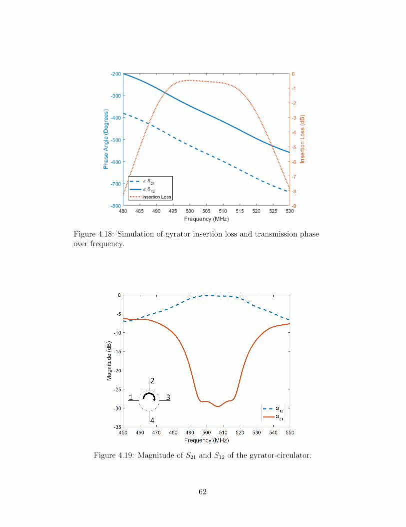
Figure 4.18: Simulation of gyrator insertion loss and transmission phaseover frequency.
Figure 4.19: Magnitude of S21 and S12 of the gyrator-circulator.
62
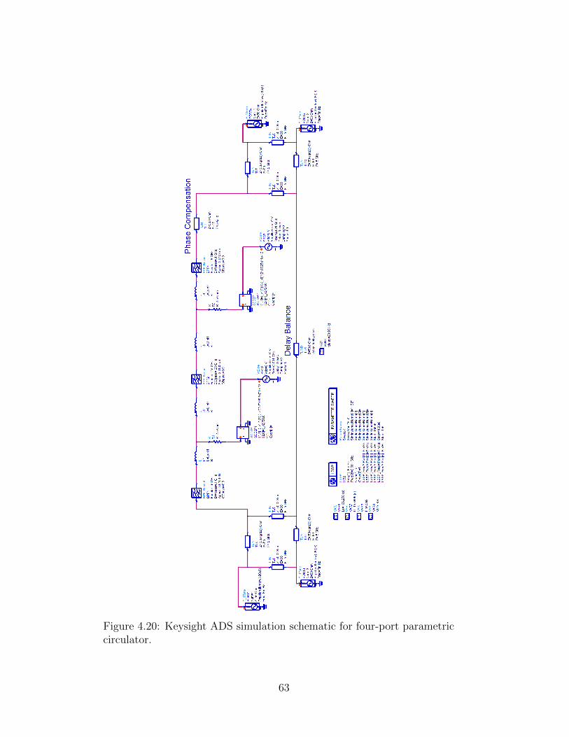
Figure 4.20: Keysight ADS simulation schematic for four-port parametriccirculator.
63

CHAPTER 5
CONCLUSION
5.1 Findings of this Work
This work has verified the findings of Kamal [12] and performed a more in-
depth analysis of the parametric gyrator and its relation to the four-port
circulator and three-port quasi-circulator. This gyrator topology has a very
wide design space, and it is still quite unexplored. There have been both
older and modern attempts to create parametric circulators [20, 21, 22], but
none have achieved any more than 5% bandwidth. Even the design exam-
ple under idealized conditions in this work only achieved 6.2% bandwidth,
but the potential of this circulator topology for much higher bandwidths is
very enticing, even though the design space still requires exploration. This
parametric gyrator has a fair share of disadvantages as well. Its performance
sensitivity to losses in the filters and nonlinear capacitors is probably its
greatest weakness. Its advantages include the need for only two nonlinear
capacitors modulated at two different LO phases (compared to the three used
in [21] with three different LO phases); the differential phase shift is inde-
pendent of frequency, which offers the potential for extreme broadbanding;
and its fairly simple design.
5.2 Areas of Future Research
Several avenues of future research in this device topology have been consid-
ered by the author.
64

5.2.1 Gyrator Loss Compensation
One major disadvantage of the parametric gyrator is the need for low-loss
filters and low-loss varactors in order to implement the device, meaning the
insertion loss of the gyrator is likely a major issue. One possible remedy for
this is the use of four-frequency parametric devices. Several researchers [23,
24, 25] have found that a hybrid parametric converter that utilizes both the
non-inverting and inverting mode at the same time can exhibit a gain higher
than the Manley-Rowe limit of f+fIF
while still maintaining a positive input
resistance. Use of such a device could be used to overcome filter losses, or
even create a gyrator with insertion gain. It is unknown to the author at this
time if such a device is practical or if the noise figure of such a device would be
considerably better or worse. Intuitively, the author believes the noise figure
would be higher, as the four-frequency devices make use of idler terminations
that can be resistive in nature, and this resistance can really only serve to add
noise to the system. Perhaps this can be acceptable if a circulator with gain
is constructed, as it could function as a low-noise amplifier for the receiver
system, and so a higher noise figure could be tolerated, since the circulator-
amplifier combination could have lower noise figure than a separate circulator
and amplifier system.
5.2.2 Gyrator with Large Tuning Range
In practice, parametric converters are often subject to narrow bandwidth.
Since the differential phase shift afforded by the gyrator is independent of
frequency, the gyrator could potentially have a large tuning range, which
could be accomplished with a variable phase shifter inline with the the gyrator
itself. At this time, a suitable topology for the parametric gyrator that could
realize this tuning feature without significantly affecting the insertion loss is
unknown to the author.
65

5.2.3 Broadening the Amplitude Bandwidth of ParametricGyrator
As one can imagine, the use of a simple tuning inductance as the matching
element in the parametric converters limits the bandwidth of the gyrator.
In order to utilize the broadbanding techniques mentioned in chapter 4, it
is imperative that the gyrator’s amplitude bandwidth be as broad as, if not
broader than, that of the hybrids to which it is connected. The author has
explored some literature that discusses the use of multiple tuning circuits
rather than just the inductance, but most promising is the theoretical work
by E. S. Kuh [26]. Experimental validation of a gyrator with more than 30%
bandwidth is necessary to eventually achieve a circulator with at least that
amount of bandwidth.
5.3 Concluding Remarks
One day, a broadband circulator could be realized using the principles dis-
cussed here. At high frequencies where the hybrid couplers are physically
small, this type of circulator could prove advantageous in communication
systems, especially if it could be used also as an amplification device. Since
the parametric circulator uses a sinusoidal LO signal to operate, it could
easily make use of the LO already present for mixing stages in communi-
cation systems. Of course, more analysis is required to determine whether
this circulator is suitable for a communication system. It seems possible to
design a gyrator with linear phase over its 3 dB bandwidth, but experimental
validation is necessary to characterize the actual harmonic distortion proper-
ties of the gyrator. Perhaps this document will be an inspiration to a future
researcher to answer these questions, just as the work of A. K. Kamal was
an inspiration to this author.
66

REFERENCES
[1] M. Faraday, “On a peculiar class of acoustical figures; and on certainforms assumed by a group of particles upon vibrating elastic surfaces,”in Phil. Trans. R. Soc. Lond., vol. 121, Jan. 1831, pp. 299–340.
[2] G. F. FitzGerald, “On the driving of electromagnetic vibrations byelectro-magnetic and electrostatic engines,” The Electrician, vol. 28, pp.329–330, Jan 1892.
[3] J. P. Gittins, J. C. Vokes, and C. S. Whitehead, “A broad-band parametric amplifier,” International Journal of Electron-ics, vol. 24, no. 4, pp. 333–351, 1968. [Online]. Available:http://dx.doi.org/10.1080/00207216808938029
[4] M. Uenohara and J. P. Elward, “Parametric amplifiers for high sensitiv-ity receivers,” IEEE Transactions on Military Electronics, vol. 8, no. 3,pp. 273–281, July 1964.
[5] M. Uenohara, M. Chruney, K. M. Eisele, D. C. Hanson, and A. L.Stillwell, “4-gc parametric amplifier for satellite communication groundstation receiver,” The Bell System Technical Journal, vol. 42, no. 4, pp.1887–1908, July 1963.
[6] K. P. Grabowski, “A nondegenerate traveling-wave parametric ampli-fier,” IRE Transactions on Microwave Theory and Techniques, vol. 10,no. 2, pp. 103–107, March 1962.
[7] P. Meerholz, “Radar sensitivity with degenerate parametric amplifierfront end,” Proceedings of the IEEE, vol. 51, no. 7, pp. 1043–1043, July1963.
[8] R. Adler and W. S. V. Slyck, “The electron beam parametric amplifier asa radar system component,” IRE Transactions on Military Electronics,vol. MIL-5, no. 2, pp. 66–71, April 1961.
[9] T. Mimura, “The early history of the high electron mobility transis-tor (hemt),” IEEE Transactions on Microwave Theory and Techniques,vol. 50, no. 3, pp. 780–782, Mar 2002.
[10] D. Pozar, Ed., Microwave Engineering. New York: Wiley, 2012.
67
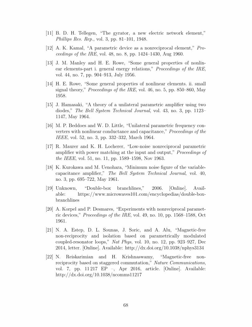
[11] B. D. H. Tellegen, “The gyrator, a new electric network element,”Phillips Res. Rep., vol. 3, pp. 81–101, 1948.
[12] A. K. Kamal, “A parametric device as a nonreciprocal element,” Pro-ceedings of the IRE, vol. 48, no. 8, pp. 1424–1430, Aug 1960.
[13] J. M. Manley and H. E. Rowe, “Some general properties of nonlin-ear elements-part i. general energy relations,” Proceedings of the IRE,vol. 44, no. 7, pp. 904–913, July 1956.
[14] H. E. Rowe, “Some general properties of nonlinear elements. ii. smallsignal theory,” Proceedings of the IRE, vol. 46, no. 5, pp. 850–860, May1958.
[15] J. Hamasaki, “A theory of a unilateral parametric amplifier using twodiodes,” The Bell System Technical Journal, vol. 43, no. 3, pp. 1123–1147, May 1964.
[16] M. P. Beddoes and W. D. Little, “Unilateral parametric frequency con-verters with nonlinear conductance and capacitance,” Proceedings of theIEEE, vol. 52, no. 3, pp. 332–332, March 1964.
[17] R. Maurer and K. H. Locherer, “Low-noise nonreciprocal parametricamplifier with power matching at the input and output,” Proceedings ofthe IEEE, vol. 51, no. 11, pp. 1589–1598, Nov 1963.
[18] K. Kurokawa and M. Uenohara, “Minimum noise figure of the variable-capacitance amplifier,” The Bell System Technical Journal, vol. 40,no. 3, pp. 695–722, May 1961.
[19] Unknown, “Double-box branchlines,” 2006. [Online]. Avail-able: https://www.microwaves101.com/encyclopedias/double-box-branchlines
[20] A. Korpel and P. Desmares, “Experiments with nonreciprocal paramet-ric devices,” Proceedings of the IRE, vol. 49, no. 10, pp. 1568–1588, Oct1961.
[21] N. A. Estep, D. L. Sounas, J. Soric, and A. Alu, “Magnetic-freenon-reciprocity and isolation based on parametrically modulatedcoupled-resonator loops,” Nat Phys, vol. 10, no. 12, pp. 923–927, Dec2014, letter. [Online]. Available: http://dx.doi.org/10.1038/nphys3134
[22] N. Reiskarimian and H. Krishnaswamy, “Magnetic-free non-reciprocity based on staggered commutation,” Nature Communications,vol. 7, pp. 11 217 EP –, Apr 2016, article. [Online]. Available:http://dx.doi.org/10.1038/ncomms11217
68

[23] D. K. Adams, “Analysis of four-frequency nonlinear reactance circuits,”IRE Transactions on Microwave Theory and Techniques, vol. 8, no. 3,pp. 274–283, May 1960.
[24] E. W. Matthews, J. A. Luksch, and G. A. VerWys, “Design and op-eration of four-frequency parametric up-converters,” IRE Transactionson Microwave Theory and Techniques, vol. 9, no. 1, pp. 44–52, January1961.
[25] A. Korpel and V. Ramaswamy, “Input conductance of a four-frequencyparametric up-converter,” IEEE Transactions on Microwave Theory andTechniques, vol. 13, no. 1, pp. 96–106, Jan 1965.
[26] E. S. Kuh, “Theory and design of wide-band parametric converters,”Proceedings of the IRE, vol. 50, no. 1, pp. 31–38, Jan 1962.
69