c511/c511a c513/c513a c513a-h - diakom.com.ru · c511/c511a c513/c513a c513a-h 8-bit cmos...
TRANSCRIPT
User’s Manual 06.96
C511/C511AC513/C513AC513A-H8-Bit CMOS Microcontroller
http://w
ww.siemens.d
e/
Semiconductor/

Edition 06.96This edition was realized using the software system FrameMaker.Published by Siemens AG,Bereich Halbleiter, Marketing-Kommunikation, Balanstraße 73,81541 München© Siemens AG 1996.All Rights Reserved.Attention please!As far as patents or other rights of third parties are concerned, liability is only assumed for components, not for applications, processes and circuits implemented within components or assemblies.The information describes the type of component and shall not be considered as assured characteristics.Terms of delivery and rights to change design reserved.For questions on technology, delivery and prices please contact the Semiconductor Group Offices in Germany or the Siemens Companies and Representatives worldwide (see address list).Due to technical requirements components may contain dangerous substances. For information on the types in question please contact your nearest Siemens Office, Semiconductor Group.Siemens AG is an approved CECC manufacturer.PackingPlease use the recycling operators known to you. We can also help you – get in touch with your nearest sales office. By agreement we will take packing material back, if it is sorted. You must bear the costs of transport. For packing material that is returned to us unsorted or which we are not obliged to accept, we shall have to invoice you for any costs in-curred.Components used in life-support devices or systems must be expressly authorized for such purpose!Critical components1 of the Semiconductor Group of Siemens AG, may only be used in life-support devices or systems2 with the express written approval of the Semiconductor Group of Siemens AG.1 A critical component is a component used in a life-support device or system whose failure can reasonably be expected to cause the
failure of that life-support device or system, or to affect its safety or effectiveness of that device or system.2 Life support devices or systems are intended (a) to be implanted in the human body, or (b) to support and/or maintain and sustain hu-
man life. If they fail, it is reasonable to assume that the health of the user may be endangered.
User’s Manual C511/C511A/C513/C513A/C513A-HRevision History : Current Version : 06.96
Previous Releases : 02.96, 05.95
Page Subjects (changes since last revision)
Several10-1410-15
Corrections of text Figure 10-12 : external clock configuration correctedUpdated package outline

Table of Contents Page
C511 / C513
1 Introduction . . . . . . . . . . . . . . . . . . . . . . . . . . . . . . . . . . . . . . . . . . . . . . . . . . . . . . . . .1-1
2 Fundamental Structure . . . . . . . . . . . . . . . . . . . . . . . . . . . . . . . . . . . . . . . . . . . . . . . .2-12.1 CPU . . . . . . . . . . . . . . . . . . . . . . . . . . . . . . . . . . . . . . . . . . . . . . . . . . . . . . . . . . . . . . . . 2-22.2 CPU Timing . . . . . . . . . . . . . . . . . . . . . . . . . . . . . . . . . . . . . . . . . . . . . . . . . . . . . . . . . . 2-4
3 Memory Organization . . . . . . . . . . . . . . . . . . . . . . . . . . . . . . . . . . . . . . . . . . . . . . . . . .3-13.1 Program Memory . . . . . . . . . . . . . . . . . . . . . . . . . . . . . . . . . . . . . . . . . . . . . . . . . . . . . . 3-23.2 Data Memory . . . . . . . . . . . . . . . . . . . . . . . . . . . . . . . . . . . . . . . . . . . . . . . . . . . . . . . . . 3-23.2.1 Internal Data Memory . . . . . . . . . . . . . . . . . . . . . . . . . . . . . . . . . . . . . . . . . . . . . . . . . . 3-23.2.2 External Data Memory . . . . . . . . . . . . . . . . . . . . . . . . . . . . . . . . . . . . . . . . . . . . . . . . . . 3-23.3 XRAM Operation (C513A/A-H only) . . . . . . . . . . . . . . . . . . . . . . . . . . . . . . . . . . . . . . . 3-33.3.1 Reset Operation of the XRAM . . . . . . . . . . . . . . . . . . . . . . . . . . . . . . . . . . . . . . . . . . . . 3-33.3.2 Accesses to XRAM using the DPTR (16-bit Addressing Mode) . . . . . . . . . . . . . . . . . . 3-33.3.3 Accesses to XRAM using the Registers R0/R1 (8-bit Addressing Mode) . . . . . . . . . . . 3-33.4 General Purpose Registers . . . . . . . . . . . . . . . . . . . . . . . . . . . . . . . . . . . . . . . . . . . . . . 3-43.5 Special Function Registers . . . . . . . . . . . . . . . . . . . . . . . . . . . . . . . . . . . . . . . . . . . . . . 3-4
4 External Bus Interface . . . . . . . . . . . . . . . . . . . . . . . . . . . . . . . . . . . . . . . . . . . . . . . . .4-14.1 Accessing External Memory . . . . . . . . . . . . . . . . . . . . . . . . . . . . . . . . . . . . . . . . . . . . . 4-14.1.1 Role of P0 and P2 as Data/Address Bus . . . . . . . . . . . . . . . . . . . . . . . . . . . . . . . . . . . 4-14.1.2 Timing . . . . . . . . . . . . . . . . . . . . . . . . . . . . . . . . . . . . . . . . . . . . . . . . . . . . . . . . . . . . . . 4-34.1.3 External Program Memory Access . . . . . . . . . . . . . . . . . . . . . . . . . . . . . . . . . . . . . . . . 4-34.2 PSEN - Program Store Enable . . . . . . . . . . . . . . . . . . . . . . . . . . . . . . . . . . . . . . . . . . . 4-34.3 ALE - Address Latch Enable . . . . . . . . . . . . . . . . . . . . . . . . . . . . . . . . . . . . . . . . . . . . . 4-34.4 XRAM Access Enable (SAB-C513A/A-H only) . . . . . . . . . . . . . . . . . . . . . . . . . . . . . . . 4-44.5 Overlapping External Data and Program Memory Spaces . . . . . . . . . . . . . . . . . . . . . . 4-4
5 System Reset . . . . . . . . . . . . . . . . . . . . . . . . . . . . . . . . . . . . . . . . . . . . . . . . . . . . . . . .5-15.1 Hardware Reset . . . . . . . . . . . . . . . . . . . . . . . . . . . . . . . . . . . . . . . . . . . . . . . . . . . . . . 5-15.2 Hardware Reset Timing . . . . . . . . . . . . . . . . . . . . . . . . . . . . . . . . . . . . . . . . . . . . . . . . . 5-2
6 On-Chip Peripheral Components . . . . . . . . . . . . . . . . . . . . . . . . . . . . . . . . . . . . . . . .6-16.1 Parallel I/O . . . . . . . . . . . . . . . . . . . . . . . . . . . . . . . . . . . . . . . . . . . . . . . . . . . . . . . . . . . 6-16.1.1 Port Structures . . . . . . . . . . . . . . . . . . . . . . . . . . . . . . . . . . . . . . . . . . . . . . . . . . . . . . . 6-16.1.2 Port 0 and Port 2 used as Address/Data Bus . . . . . . . . . . . . . . . . . . . . . . . . . . . . . . . . 6-86.1.3 Alternate Functions . . . . . . . . . . . . . . . . . . . . . . . . . . . . . . . . . . . . . . . . . . . . . . . . . . . . 6-96.1.4 Port Handling . . . . . . . . . . . . . . . . . . . . . . . . . . . . . . . . . . . . . . . . . . . . . . . . . . . . . . . . 6-126.1.4.1 Port Timing . . . . . . . . . . . . . . . . . . . . . . . . . . . . . . . . . . . . . . . . . . . . . . . . . . . . . . . . . 6-126.1.4.2 Port Loading and Interfacing . . . . . . . . . . . . . . . . . . . . . . . . . . . . . . . . . . . . . . . . . . . . 6-136.1.4.3 Read-Modify-Write Feature of Ports 1, 2 and 3 . . . . . . . . . . . . . . . . . . . . . . . . . . . . . . 6-136.2 Timers/Counters . . . . . . . . . . . . . . . . . . . . . . . . . . . . . . . . . . . . . . . . . . . . . . . . . . . . . 6-156.2.1 Timer/Counter 0 and 1 . . . . . . . . . . . . . . . . . . . . . . . . . . . . . . . . . . . . . . . . . . . . . . . . 6-166.2.1.1 Mode 0 . . . . . . . . . . . . . . . . . . . . . . . . . . . . . . . . . . . . . . . . . . . . . . . . . . . . . . . . . . . . 6-186.2.1.2 Mode 1 . . . . . . . . . . . . . . . . . . . . . . . . . . . . . . . . . . . . . . . . . . . . . . . . . . . . . . . . . . . . 6-196.2.1.3 Mode 2 . . . . . . . . . . . . . . . . . . . . . . . . . . . . . . . . . . . . . . . . . . . . . . . . . . . . . . . . . . . . 6-206.2.1.4 Mode 3 . . . . . . . . . . . . . . . . . . . . . . . . . . . . . . . . . . . . . . . . . . . . . . . . . . . . . . . . . . . . 6-216.2.2 Timer/Counter 2 (SAB-C513/C513A/C513A-H only) . . . . . . . . . . . . . . . . . . . . . . . . . 6-22
Semiconductor Group I-1

Table of Contents Page
C511 / C513
6.2.2.1 Auto-Reload Mode (Up or Down Counter) . . . . . . . . . . . . . . . . . . . . . . . . . . . . . . . . . 6-246.2.2.2 Capture Mode . . . . . . . . . . . . . . . . . . . . . . . . . . . . . . . . . . . . . . . . . . . . . . . . . . . . . . . 6-266.3 General Purpose Serial Interface USART (SAB-C513/C513AC513A-H only) . . . . . . 6-276.3.1 Multiprocessor Communications . . . . . . . . . . . . . . . . . . . . . . . . . . . . . . . . . . . . . . . . . 6-286.3.2 Serial Port Control Register . . . . . . . . . . . . . . . . . . . . . . . . . . . . . . . . . . . . . . . . . . . . . 6-296.3.3 Baud Rates . . . . . . . . . . . . . . . . . . . . . . . . . . . . . . . . . . . . . . . . . . . . . . . . . . . . . . . . . 6-306.3.3.1 Using Timer 1 to Generate Baud Rates . . . . . . . . . . . . . . . . . . . . . . . . . . . . . . . . . . . 6-316.3.3.2 Using Timer 2 to Generate Baud Rates . . . . . . . . . . . . . . . . . . . . . . . . . . . . . . . . . . . 6-326.3.4 Details about Mode 0 . . . . . . . . . . . . . . . . . . . . . . . . . . . . . . . . . . . . . . . . . . . . . . . . . 6-346.3.5 Details about Mode 1 . . . . . . . . . . . . . . . . . . . . . . . . . . . . . . . . . . . . . . . . . . . . . . . . . 6-376.3.6 Details about Modes 2 and 3 . . . . . . . . . . . . . . . . . . . . . . . . . . . . . . . . . . . . . . . . . . . . 6-406.4 Synchronous Serial Channel (SSC) . . . . . . . . . . . . . . . . . . . . . . . . . . . . . . . . . . . . . . 6-436.4.1 SSC Block Diagram . . . . . . . . . . . . . . . . . . . . . . . . . . . . . . . . . . . . . . . . . . . . . . . . . . . 6-436.4.2 General Operation of the SSC . . . . . . . . . . . . . . . . . . . . . . . . . . . . . . . . . . . . . . . . . . 6-446.4.3 Enable/Disable Control . . . . . . . . . . . . . . . . . . . . . . . . . . . . . . . . . . . . . . . . . . . . . . . . 6-446.4.4 Baudrate Generation (Master Mode only) . . . . . . . . . . . . . . . . . . . . . . . . . . . . . . . . . . 6-456.4.5 Write Collision Detection . . . . . . . . . . . . . . . . . . . . . . . . . . . . . . . . . . . . . . . . . . . . . . . 6-456.4.6 Master/Slave Mode Selection . . . . . . . . . . . . . . . . . . . . . . . . . . . . . . . . . . . . . . . . . . . 6-466.4.7 Data/Clock Timing Relationships . . . . . . . . . . . . . . . . . . . . . . . . . . . . . . . . . . . . . . . . 6-476.4.7.1 Master Mode Operation . . . . . . . . . . . . . . . . . . . . . . . . . . . . . . . . . . . . . . . . . . . . . . . . 6-476.4.7.2 Slave Mode Operation . . . . . . . . . . . . . . . . . . . . . . . . . . . . . . . . . . . . . . . . . . . . . . . . . 6-486.4.8 Register Description . . . . . . . . . . . . . . . . . . . . . . . . . . . . . . . . . . . . . . . . . . . . . . . . . . 6-496.4.8.1 SSC Control Register SSCCON . . . . . . . . . . . . . . . . . . . . . . . . . . . . . . . . . . . . . . . . . 6-496.4.8.2 SSC Interrupt Enable Register SCIEN . . . . . . . . . . . . . . . . . . . . . . . . . . . . . . . . . . . . 6-516.4.8.3 Status Register SCF . . . . . . . . . . . . . . . . . . . . . . . . . . . . . . . . . . . . . . . . . . . . . . . . . . 6-526.4.8.4 Data Registers STB and SRB . . . . . . . . . . . . . . . . . . . . . . . . . . . . . . . . . . . . . . . . . . . 6-536.4.8.5 Mode Test Register SSCMOD . . . . . . . . . . . . . . . . . . . . . . . . . . . . . . . . . . . . . . . . . . 6-536.4.8.6 Location of Bitaddressable Control and Status Bits . . . . . . . . . . . . . . . . . . . . . . . . . . 6-54
7 Interrupt System . . . . . . . . . . . . . . . . . . . . . . . . . . . . . . . . . . . . . . . . . . . . . . . . . . . . . .7-17.1 Interrupt Structure . . . . . . . . . . . . . . . . . . . . . . . . . . . . . . . . . . . . . . . . . . . . . . . . . . . . . 7-37.2 Interrupt Control Bits . . . . . . . . . . . . . . . . . . . . . . . . . . . . . . . . . . . . . . . . . . . . . . . . . . . 7-47.2.1 Interrupt Enables . . . . . . . . . . . . . . . . . . . . . . . . . . . . . . . . . . . . . . . . . . . . . . . . . . . . . . 7-47.2.2 Interrupt Priorities . . . . . . . . . . . . . . . . . . . . . . . . . . . . . . . . . . . . . . . . . . . . . . . . . . . . . 7-57.3 How Interrupts are Handled . . . . . . . . . . . . . . . . . . . . . . . . . . . . . . . . . . . . . . . . . . . . . 7-77.4 External Interrupts . . . . . . . . . . . . . . . . . . . . . . . . . . . . . . . . . . . . . . . . . . . . . . . . . . . . . 7-87.5 Response Time . . . . . . . . . . . . . . . . . . . . . . . . . . . . . . . . . . . . . . . . . . . . . . . . . . . . . . . 7-9
8 Power Saving Modes . . . . . . . . . . . . . . . . . . . . . . . . . . . . . . . . . . . . . . . . . . . . . . . . . .8-18.1 Idle Mode . . . . . . . . . . . . . . . . . . . . . . . . . . . . . . . . . . . . . . . . . . . . . . . . . . . . . . . . . . . . 8-28.2 Power-Down Mode . . . . . . . . . . . . . . . . . . . . . . . . . . . . . . . . . . . . . . . . . . . . . . . . . . . . 8-4
9 EEPROM Programming Interface of the SAB-C513A-H . . . . . . . . . . . . . . . . . . . . . .9-19.1 Programming Configuration . . . . . . . . . . . . . . . . . . . . . . . . . . . . . . . . . . . . . . . . . . . . . 9-19.2 Programming Interface . . . . . . . . . . . . . . . . . . . . . . . . . . . . . . . . . . . . . . . . . . . . . . . . . 9-49.2.1 Selection of the Programming Mode . . . . . . . . . . . . . . . . . . . . . . . . . . . . . . . . . . . . . . . 9-59.2.2 Resetting the Programming Interface . . . . . . . . . . . . . . . . . . . . . . . . . . . . . . . . . . . . . . 9-5
Semiconductor Group I-2

Table of Contents Page
C511 / C513
9.2.3 Interface Bus Operation . . . . . . . . . . . . . . . . . . . . . . . . . . . . . . . . . . . . . . . . . . . . . . . . 9-59.2.4 Programming Interface Registers . . . . . . . . . . . . . . . . . . . . . . . . . . . . . . . . . . . . . . . . . 9-79.2.4.1 Programming Control Register PCNTRL . . . . . . . . . . . . . . . . . . . . . . . . . . . . . . . . . . . 9-89.2.4.2 Memory Select Register PMSEL . . . . . . . . . . . . . . . . . . . . . . . . . . . . . . . . . . . . . . . . . . 9-99.2.4.3 Data Register PDATA . . . . . . . . . . . . . . . . . . . . . . . . . . . . . . . . . . . . . . . . . . . . . . . . . 9-109.2.4.4 Address Low Register PADRL and PADRH . . . . . . . . . . . . . . . . . . . . . . . . . . . . . . . . 9-109.2.5 EEPROM Access Operations . . . . . . . . . . . . . . . . . . . . . . . . . . . . . . . . . . . . . . . . . . . 9-119.2.5.1 Erase Operation . . . . . . . . . . . . . . . . . . . . . . . . . . . . . . . . . . . . . . . . . . . . . . . . . . . . . 9-119.2.5.2 Write Operation . . . . . . . . . . . . . . . . . . . . . . . . . . . . . . . . . . . . . . . . . . . . . . . . . . . . . . 9-129.2.5.3 Read Operation . . . . . . . . . . . . . . . . . . . . . . . . . . . . . . . . . . . . . . . . . . . . . . . . . . . . . . 9-12
10 Device Specifications . . . . . . . . . . . . . . . . . . . . . . . . . . . . . . . . . . . . . . . . . . . . . . .10-1310.1 Absolute Maximum Ratings . . . . . . . . . . . . . . . . . . . . . . . . . . . . . . . . . . . . . . . . . . . . 10-1310.2 DC Characteristics . . . . . . . . . . . . . . . . . . . . . . . . . . . . . . . . . . . . . . . . . . . . . . . . . . 10-1410.3 AC Characteristics (applies to all C511/513 Family Microcontrollers) . . . . . . . . . . . . 10-1610.3.1 Program Memory Characteristics . . . . . . . . . . . . . . . . . . . . . . . . . . . . . . . . . . . . . . . 10-1610.3.2 External Data Memory Characteristics . . . . . . . . . . . . . . . . . . . . . . . . . . . . . . . . . . . 10-1710.3.3 SSC Interface Characteristics . . . . . . . . . . . . . . . . . . . . . . . . . . . . . . . . . . . . . . . . . . 10-1810.3.4 External Clock Characteristics . . . . . . . . . . . . . . . . . . . . . . . . . . . . . . . . . . . . . . . . . 10-1810.3.5 ROM Verification Characteristics (only C511/C511A/C513/C513A) . . . . . . . . . . . . 10-2210.4 AC Characteristics of C513A-H Programming Interface . . . . . . . . . . . . . . . . . . . . . . 10-2310.4.1 Reset Characteristics (C513A-H only) . . . . . . . . . . . . . . . . . . . . . . . . . . . . . . . . . . . 10-2510.5 Package Outlines . . . . . . . . . . . . . . . . . . . . . . . . . . . . . . . . . . . . . . . . . . . . . . . . . . . 10-27
Semiconductor Group I-3

Introduction
1 Introduction
The C511-R, C511A-R, C513-R, C513A-R, C513A-2R, and C513A-H are members of a family oflow cost microcontrollers, which are software compatible with the components of the SAB 8051,SAB 80C51 and C500 families.
The five versions with the “-R” extension contain a non-volatile read-only program memory (ROM).The C513A-H is a version with a 12 Kbyte EEPROM instead of ROM. This device can be used forprototype designs which have a demand for reprogrammable on-chip code memory.
The microcontroller versions differ in functionality according table 1-1. They offer different ROMsizes, different RAM/XRAM sizes and a different timer/USART configuration. Common to alldevices is an advanced SSC serial port, a second synchronous serial interface, which is compatibleto the SPI serial bus industry standard. Except the EEPROM size, the functionality of the C513A-His a superset of all ROM versions of the C511/513 family.
In this user manual the microcontroller family is also referenced with the term C511/513 and theROM versions are referenced without the “-R” extension. If some of the features described areapplicable to selected family members only, this will be explicitly stated.
Table 1-1Functionality of the C511/513 MCUs
Note: 1) T0 and T1 are the standard 16-bit timer. T2 is the 16-bit timer with autoreload.2) USART is the Universal Synchronous/Asynchronous Receive/Transmit interface.3) SSC is the Synchronous Serial Channel (SPI compatible interface).
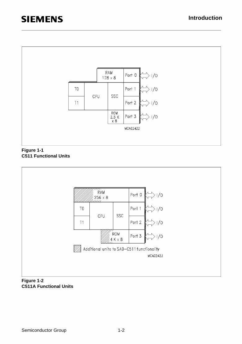
According table 1-1, figure 1-1 to figure 1-4 show the functional units of the members of the C511/513 family microcontrollers.
Device ROM Size
EEPROM Size
RAM Size
XRAM Size
Timers 1) USART 2) SSC 3)
C511 2.5 KB – 128 B – T0, T1 –
C511A 4 KB – 256 B – T0, T1 –
C513 8 KB – 256 B – T0, T1, T2
C513A 12/16 KB – 256 B 256 B T0, T1, T2
C513A-H – 12 KB 256 B 256 B T0, T1, T2
Semiconductor Group 1-1
Introduction
Figure 1-1C511 Functional Units
Figure 1-2C511A Functional Units
Semiconductor Group 1-2

Introduction
Figure 1-3C513 Functional Units
Figure 1-4C513A / C513A-H Functional Units
Semiconductor Group 1-3

Introduction
Listed below is a summary of the main features of the C511/513 family members:
– Fully software compatible to standard 8051/8052 microcontrollers
– Up to 12 MHz operating frequency
– Up to 12 K×8 ROM / EEPROM
– Up to 256×8 RAM
– Up to 256x8 XRAM
– Four 8-bit ports
– Up to three 16-bit Timers / Counters (Timer 2 with Up/Down and 16-bit autoreload feature)
– Synchronous Serial Channel (SSC)
– Optional USART
– Up to seven interrupt sources, two priority levels
– Power Saving Modes
– P-LCC-44 package (C513A also in P-MQFP-44 package)
– Temperature ranges: SAB-C511 / 511A / 513 / 513A / C513A-H TA : 0 °C to 70 °CSAF-C513A TA : -40 °C to 85 °C
Figure 1-5C511/C513 Logic Symbol
If the C513A-H is used in programming mode, its logic symbol is different from figure 1-5 (seefigure 9-1).
Semiconductor Group 1-4

Introduction
Pin Configuration(top view)
Figure 1-6P-LCC-44 Package Pin Configuration (Top View)
Semiconductor Group 1-5

Introduction
Figure 1-7 P-MQFP-44 Package Pin Configuration of the C513A (Top View)
If the C513A-H is used in programming mode, the pin configuration is different to figure 1-6 orfigure 1-7. (see figure 9-2)
If the C513A-H is used in programming mode, the pin definitions and functions are different to table1-2 (see table 9-1).
Semiconductor Group 1-6

Introduction
Table 1-2Pin Definitions and Functions
Symbol Pin Number I/O*) Function
P-LCC-44
P-MQFP-44
P1.7-P1.0 9-2
23
4
567
3-1, 44-40
4041
42
43441
I/O Port 1is a bidirectional I/O port with internal pull-up resistors. Port 1 pins that have 1s written to them are pulled high by the internal pullup resistors, and in that state can be used as inputs. As inputs, port 1 pins being externally pulled low will source current (IIL, in the DC characteristics) because of the internal pullup resistors. Port 1 also contains the timer 2 and SSC pins as secondary function. In general the output latch corresponding to a secondary function must be programmed to a one (1) for that function to operate.For the outputs of the SSC (SCLK, STO) special circuitry is implemented, providing true push-pull capability. The STO output in addition will have true tristate capability.When used for SSC inputs, the pull-up resistors will be switched off and the inputs will float (high ohmic inputs).
The alternate functions are assigned to port 1, as follows:
P1.0 T2 Input to counter 2 1)
P1.1 T2EX Capture -Reload trigger of timer 2 1)
Up-Down countP1.2 SCLK SSC Master Clock Output
SSC Slave Clock InputP1.3 SRI SSC Receive InputP1.4 STO SSC Transmit OutputP1.5 SLS Slave Select Input
1) not available in the C511/511A
*) I = InputO = Output
Semiconductor Group 1-7

Introduction
P3.0-P3.7 11,13-19
11
13
1415161718
19
5, 7-13
5
7
89101112
13
I/O Port 3is a bidirectional I/O port with internal pull-up resistors. Port 3 pins that have 1s written to them are pulled high by the internal pullup resistors, and in that state can be used as inputs. As inputs, port 3 pins being externally pulled low will source current (IIL, in the DC characteristics) because of the internal pullup resistors. Port 3 also contains the interrupt, timer, serial port and external memory strobe pins that are used by various options. The output latch corresponding to a secondary function must be programmed to a one (1) for that function to operate.
The secondary functions are assigned to the pins of port 3 as follows:
P3.0 RXD Receiver data input (asynchronous) or data input/output (synchronous)of serial interface (USART) 1)
P3.1 TXD Transmitter data output (USART) 1)
(asynchronous) or clock output(synchronous) of serial interface
P3.2 INT0 Interrupt 0 input / timer 0 gate controlP3.3 INT1 Interrupt 1 input / timer 1 gate controlP3.4 T0 Counter 0 inputP3.5 T1 Counter 1 inputP3.6 WR Write control signal : latches the data
byte from port 0 into the externaldata memory
P3.7 RD Read control signal : enables theexternal data memory to port 0
1) not available in the C511/511A
XTAL2 20 14 – XTAL2Output of the inverting oscillator amplifier.
*) I = InputO = Output
Table 1-2Pin Definitions and Functions (cont’d)
Symbol Pin Number I/O*) Function
P-LCC-44
P-MQFP-44
Semiconductor Group 1-8

Introduction
XTAL1 21 15 – XTAL1Input to the inverting oscillator amplifier and input to the internal clock generator circuits.To drive the device from an external clock source, XTAL1 should be driven, while XTAL2 is left unconnected. There are no requirements on the duty cycle of the external clock signal, since the input to the internal clocking circuitry is divided down by a divide-by-two flip-flop. Minimum and maximum high and low times as well as rise/fall times specified in the AC characteristics must be observed.
P2.0-P2.7 24-31 18-25 I/O Port 2is a bidirectional I/O port with internal pullup resistors. Port 2 pins that have 1s written to them are pulled high by the internal pullup resistors, and in that state can be used as inputs. As inputs, port 2 pins being externally pulled low will source current (IIL, in the DC characteristics) because of the internal pullup resistors. Port 2 emits the high-order address byte during fetches from external program memory and during accesses to external data memory that use 16-bit addresses (MOVX @DPTR). In this application it uses strong internal pullup resistors when issuing 1s. During accesses to external data memory that use 8-bit addresses (MOVX @Ri), port 2 issues the contents of the P2 special function register.
PSEN 32 26 O The Program Store Enableoutput is a control signal that enables the external program memory to the bus during external fetch operations. It is activated every six oscillator periodes except during external data memory accesses. Remains high during internal program execution.
RESET 10 4 I RESETA high level on this pin for two machine cycles while the oscillator is running resets the device. An internal resistor to VSS permits power-on reset using only an external capacitor to VCC.
*) I = InputO = Output
Table 1-2Pin Definitions and Functions (cont’d)
Symbol Pin Number I/O*) Function
P-LCC-44
P-MQFP-44
Semiconductor Group 1-9

Introduction
ALE 33 27 O The Address Latch Enableoutput is used for latching the low-byte of the address into external memory during normal operation. It is activated every six oscillator periodes except during an external data memory access.If no external memory is used, the ALE signal generation can be inhibited, reducing system RFI, by clearing register bit EALE in the SYSCON register.
EA 35 29 I External Access EnableWhen held at high level, instructions are fetched from the internal ROM when the PC is less than the size of the internal ROM : C511 0A00H
C511A 1000HC513 2000HC513A/A-H 3000HC513A-2R 4000H
When held at low level, the microcontroller fetches all instructions from external program memory.
P0.0-P0.7 43-36 37-30 I/O Port 0is an 8-bit open-drain bidirectional I/O port. Port 0 pins that have 1s written to them float, and in that state can be used as high-impendance inputs. Port 0 is also the multiplexed low-order address and data bus during accesses to external program or data memory. In this application it uses strong internal pullup transistors when issuing 1s. External pullup resistors are required during program verification.
VSS 22 16 – Circuit ground potential
VCC 44 38 – Power Supply terminal for all operating modes
N.C. 1, 12,23, 34
6, 17,28, 39
– No connection, do not connect externally
*) I = InputO = Output
Table 1-2Pin Definitions and Functions (cont’d)
Symbol Pin Number I/O*) Function
P-LCC-44
P-MQFP-44
Semiconductor Group 1-10

Fundamental Structure
2 Fundamental Structure
The SAB-C511/513 family microcontrollers are based on the SAB-C501 architecture. Thereforethey are also fully compatible to the standard 8051 microcontroller family.
The completely new units compared to the SAB-C501 are the synchronous serial channel, theXRAM, and the EEPROM code memory.
Figure 2-8 shows a block diagram of the SAB-C511/513 family microcontrollers.
Figure 2-8Block Diagram of the SAB-C511/513
Semiconductor Group 2-1

Fundamental Structure
2.1 CPU
The SAB-C511/513 microcontrollers are efficient both as a controller and as an arithmeticprocessor. It have extensive facilities for binary and BCD arithmetic and excels in its bit-handlingcapabilities. Efficient use of program memory results from an instruction set consisting of 44% one-byte, 41% two-byte, and 15% three-byte instructions. With an 8 MHz clock, 58% of the instructionsare executed in 1.5 µs.
The CPU (Central Processing Unit) of the SAB-C511/513 consists of the instruction decoder, thearithmetic section and the program control section. Each program instruction is decoded by theinstruction decoder. This unit generates the internal signals controlling the functions of the individualunits within the CPU. They have an effect on the source and destination of data transfers, andcontrol the ALU processing.
The arithmetic section of the processor performs extensive data manipulation and is comprised ofthe arithmetic/logic unit (ALU), an A register, B register and PSW register.
The ALU accepts 8-bit data words from one or two sources and generates an 8-bit result under thecontrol of the instruction decoder. The ALU performs the arithmetic operations add, substract,multiply, divide, increment, decrement, BDC-decimal-add-adjust and compare, and the logicoperations AND, OR, Exclusive OR, complement and rotate (right, left or swap nibble (left four)).Also included is a Boolean processor performing the bit operations as set, clear, completement,jump-if-not-set, jump-if-set-and-clear and move to/from carry. Between any addressable bit (or itscomplement) and the carry flag, it can perform the bit operations of logical AND or logical OR withthe result returned to the carry flag.
The program control section controls the sequence in which the instructions stored in programmemory are executed. The 16-bit program counter (PC) holds the address of the next instruction tobe executed. The conditional branch logic enables internal and external events to the processor tocause a change in the program execution sequence.
Accumulator
ACC is the symbol for the accumulator register. The mnemonics for accumulator-specificinstructions, however, refer to the accumulator simply as A.
Program Status Word
The Program Status Word (PSW) contains several status bits that reflect the current state of theCPU.
Semiconductor Group 2-2

Fundamental Structure
Special Function Register PSW (Address D0H) Reset Value : 00H
B Register
The B register is used during multiply and divide and serves as both source and destination. Forother instructions it can be treated as another scratch pad register.
Stack Pointer
The stack pointer (SP) register is 8 bits wide. It is incremented before data is stored during PUSHand CALL executions and decremented after data is popped during a POP and RET (RETI)execution, i.e. it always points to the last valid stack byte. While the stack may reside anywhere inthe on-chip RAM, the stack pointer is initialized to 07H after a reset. This causes the stack to begina location = 08H above register bank zero. The SP can be read or written under software control.
Bit Function
CY Carry Flag
AC Auxiliary Carry Flag (for BCD operations)
F0 General Purpose Flag
RS1 RS00 00 11 01 1
Register Bank select control bitsBank 0 selected, data address 00H-07HBank 1 selected, data address 08H-0FHBank 2 selected, data address 10H-17HBank 3 selected, data address 18H-1FH
OV Overflow Flag
F1 General Purpose Flag
P Parity FlagSet/cleared by hardware each instruction cycle to indicate an odd/even number of "one" bits in the accumulator, i.e. even parity.
CY AC F0 RS1D0H PSW
Bit No. 7 6 5 4 3 2 1 0MSB LSB
RS0 OV F1 P
Semiconductor Group 2-3

Fundamental Structure
2.2 CPU Timing
A machine cycle consists of 6 states (12 oscillator periods). Each state is devided into a phase 1half, during which the phase 1 clock is active, and a phase 2 half, during which the phase 2 clock isactive. Thus, a machine cycle consists of 12 oscillator periods, numbered S1P1 (state 1, phase 1)through S6P2 (state 6, phase 2). Each state lasts for two oscillator periods. Typically, arithmetic andlogical operations take place during phase 1 and internal register-to-register transfers take placeduring phase 2.
The diagrams in figure 2-2-9 show the fetch/execute timing related to the internal states andphases. Since these internal clock signals are not user-accessible, the XTAL2 oscillator signals andthe ALE (address latch enable) signal are shown for external reference. ALE is normally activatedtwice during each machine cycle: once during S1P2 and S2P1, and again during S4P2 and S5P1.
Executing of a one-cycle instruction begins at S1P2, when the op-code is latched into the instructionregister. If it is a two-byte instruction, the second reading takes place during S4 of the samemachine cycle. If it is a one-byte instruction, there is still a fetch at S4, but the byte read (which wouldbe the next op-code) is ignored (discarded fetch), and the program counter is not incremented. Inany case, execution is completed at the end of S6P2.
Figures 2-2-9 a) and b) show the timing of a 1-byte, 1-cycle instruction and for a 2-byte, 1-cycleinstruction.
Most SAB-C511/513 instructions are executed in one cycle. MUL (multiply) and DIV (divide) are theonly instructions that take more than two cycles to complete; they take four cycles. Normally twocode bytes are fetched from the program memory during every machine cycle. The only exceptionto this is when a MOVX instruction is executed. MOVX is a one-byte, 2-cycle instruction thataccesses external data memory. During a MOVX, the two fetches in the second cycle are skippedwhile the external data memory is being addressed and strobed. Figure 2-2-9 c) and d) show thetiming for a normal 1-byte, 2-cycle instruction and for a MOVX instruction.
Semiconductor Group 2-4

Fundamental Structure
Figure 2-9Fetch Execute Sequence
Semiconductor Group 2-5

Memory Organization
3 Memory Organization
The C511/513 CPU manipulates operands in the following four address spaces:
– up to 64 Kbyte of external program memory– up to 16 Kbyte of internal program memory– up to 64 Kbyte of external data memory– up to 256 bytes of internal data memory (includes bitaddressable area of 128 bits)– 256 bytes additional internal data memory (XRAM)– a 128 byte special function register area with 16 bitaddressable registers (128 bits)
Figure 3-10 illustrates the memory address spaces of the C511/513.
Figure 3-10Memory Map
Semiconductor Group 3-1

Memory Organization
3.1 Program Memory
The C511/513 family members have up to 12 Kbytes of on-chip read-only program memory(depending on version). The program memory can be externally expanded up to 64 Kbytes. If theEA pin is held high, the C511/513 executes out of internal ROM unless the address exceeds theupper limit of the on-chip program memory (upper limit table see figure 3-10). Instructions ataddresses above this limit are then fetched from the external program memory. If the EA pin is heldlow, the C511/513 fetches all instructions from the external program memory.
3.2 Data Memory
The data memory address space consists of an internal and an external memory space. Thedifferent versions of the C511/513 microcontroller family provide 128 (C511 only) or 256 byte (allother members) of internal data memory.
The C513A/A-H contain another 256 byte of on-chip RAM additional to its 256 byte internal RAM.This RAM is referenced as XRAM (‘eXtended RAM’).
3.2.1 Internal Data Memory
The internal data memory is divided into four physically separate and distinct blocks:
– the lower 128 byte of RAM including four register banks containing eight registers each– the upper 128 byte of RAM– the 128 byte special function register area– a 256 byte XRAM area which is accessed like external RAM (MOVX-instructions), but is
implemented on-chip (C513A/A-H only).
3.2.2 External Data Memory
Up to 64 Kbyte external data memory can be addressed by instructions that use 8-bit or 16-bitindirect addressing. A 16-bit external memory addressing mode is supported by the MOVXinstructions using the 16-bit datapointer DPTR for addressing. For 8-bit addressing MOVXinstructions in combination with registers R0 and R1 can be used.
Note that there are restrictions with the C513A/A-H and 8-bit addressing mode when accessingexternal data memory (details see chapters 3.3.2 and 3.3.3).
Semiconductor Group 3-2

Memory Organization
3.3 XRAM Operation (C513A/A-H only)
The XRAM is a memory area that is logically located in the external memory space, but is integratedon the chip. Because the XRAM is used in the same way as external data memory the sameinstruction types must be used for accessing the XRAM. The XRAM can be enabled and disabledby the XMAP bit in the SYSCON register (see chapter 4.4).
3.3.1 Reset Operation of the XRAM
The content of the XRAM is not affected by a reset. After power-up the content is undefined, whileit remains unchanged during and after a reset as long as the power supply is not turned off.
If a reset occurs during a write operation to XRAM, the content of a XRAM memory locationdepends on the cycle which the reset is detected at (MOVX is a 2-cycle instruction):
Reset during 1st cycle : The new value will not be written to XRAM. The old value is not affected.Reset during 2nd cycle : The old value in XRAM is overwritten by the new value.
After reset the XRAM is disabled.
3.3.2 Accesses to XRAM using the DPTR (16-bit Addressing Mode)
There are a read and a write instruction to access the XRAM which use the 16-bit DPTR for indirectaddressing. The instructions are :
– MOVX A, @DPTR (Read)– MOVX @DPTR, A (Write)
Use of these instructions normally implies, that port 0 is used as address low/data bus, port 2 forhigh address output and parts of port 3 for control to access upto 64 KB of external memory. If theXRAM is disabled, this will happen as with the other members of the C511/513 family. If it is enabledand if the effective address is in the range of 0000H to FEFFH, these instruction also will accessexternal memory.
If XRAM is enabled and if the address is within FF00H to FFFFH, the physically internal XRAM ofthe C513A/A-H will be accessed. Physically external memory in this address range cannot beaccessed in this case, because no external bus cycles will generated. Therefore port 0, 2 and 3 canbe used as general purpose I/O if only the XRAM memory space is addressed by the user program.
3.3.3 Accesses to XRAM using the Registers R0/R1 (8-bit Addressing Mode)
The C511/513 architecture provides also instructions for accesses to external data memory whichuse only an 8-bit address (indirect addressing with registers R0 or R1). These instructions are :
– MOVX A, @Ri (Read)– MOVX @Ri, A (Write)
Use of these instructions implies, that port 0 is used as address/data bus, port 2 for high addressoutput and parts of port 3 for control. Normally these instructions are used to access up to 256 byteof external memory.
If the XRAM is disabled, this will happen as with the other members of the C511/513 componentsand the external memory is accessed.
Semiconductor Group 3-3

Memory Organization
If the XRAM is enabled these instruction will only access the internal XRAM. External memorycannot be accessed in this case because no external bus cycle will be generated. Therefore, port0 and 3 can be used as standard I/O, if only the internal XRAM is used.
3.4 General Purpose Registers
The lower 32 locations of the internal RAM are assigned to four banks with eight general purposeregisters (GPRs) each. Only one of these banks may be enabled at a time. Two bits in the programstatus word PSW, RS1 and RS0, select the active register bank (see description of the PSW inchapter 2.1). This allows fast context switching, which is useful when entering subroutines orinterrupt service routines. After reset register bank 0 is selected.
The 8 general purpose registers of the selected register bank may be accessed by registeraddressing. With register addressing the instruction opcode indicates which register is to be used.For indirect addressing R0 and R1 are used as pointer or index register to address internal orexternal memory (e.g. MOV @R0).
Reset initializes the stack pointer to location 07H and increments it once to start from location 08Hwhich is also the first register (R0) of register bank 1. Thus, if one is going to use more than oneregister bank, the SP should be initialized to a different location of the RAM which is not used fordata storage.
3.5 Special Function Registers
All registers except the program counter and the four general purpose register banks reside in thespecial function register area.
The 34 special function registers (SFR) include pointers and registers that provide an interfacebetween the CPU and the other on-chip peripherals. There are also 128 directly addressable bitswithin the SFR area.
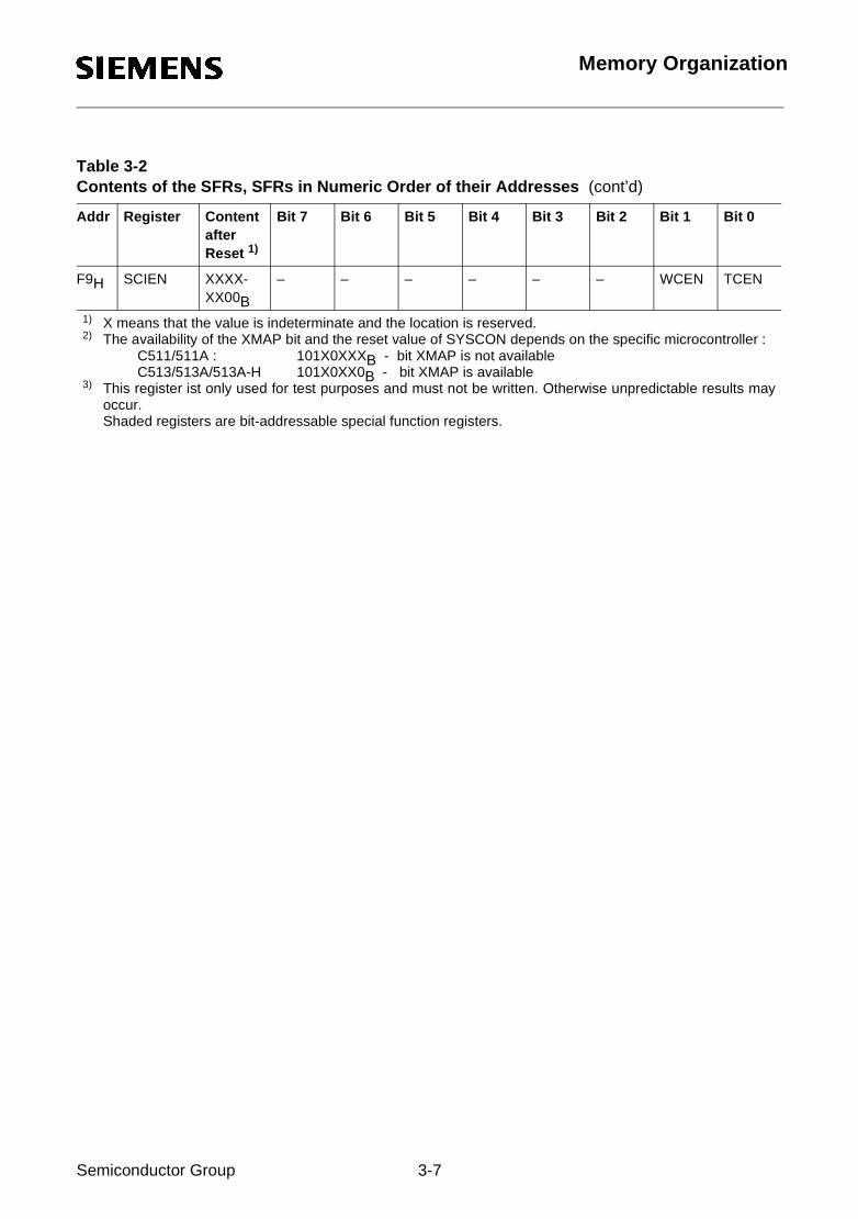
All SFRs are listed in table 3-1 and table 3-2. In table 3-1 they are organized in groups which referto the functional blocks of the C511/513. Table 3-2 illustrates the contents of the SFRs, e.g. the bitsof the SFRs.
Table 3-2 Contents of the SFRs, SFRs in Numeric Order of their Addresses
Addr Register Content after Reset 1)
Bit 7 Bit 6 Bit 5 Bit 4 Bit 3 Bit 2 Bit 1 Bit 0
80H P0 FFH .7 .6 .5 .4 .3 .2 .1 .0
81H SP 07H .7 .6 .5 .4 .3 .2 .1 .0
82H DPL 00H .7 .6 .5 .4 .3 .2 .1 .0
83H DPH 00H .7 .6 .5 .4 .3 .2 .1 .0
Semiconductor Group 3-4

Memory Organization
Table 3-1SFRs - Functional Blocks
Block Symbol Name Address Contents afterReset
CPU ACCBDPHDPLPSWSPSYSCON
AccumulatorB-RegisterData Pointer, High ByteData Pointer, Low ByteProgram Status WordStack PointerSystem Control Reg. C511/C511A
C513/C513A/C513A-H
E0H 1)
F0H 1)
83H82HD0H
1) 81HB1HB1H
00H00H00H00H00H07H101X0XXXB
3)
101X0XX0B 3)
InterruptSystem
IEIP
Interrupt Enable RegisterInterrupt Priority Register
A8H1)
B8H 1)
00HX0000000B
3)
Ports P0
P1P2P3
Port 0Port 1Port 2Port 3
80H 1)
90H 1)
A0H 1)
B0H 1)
FFHFFHFFHFFH
SSC SSCCONSTBSRBSCFSCIENSSCMOD
SSC Control RegisterSSC Transmit BufferSSC Receive RegisterSSC Flag RegisterSSC Interrupt Enable RegisterSSC Mode Test Register
E8H 1)
E9HEAHF8H
1)
F9HEBH
07HXXH
3)XXH
3)XXXXXX00B
3) XXXXXX00B
3) 00H
USART PCON 2)
SBUFSCON
Power Control RegisterSerial Channel Buffer RegisterSerial Channel 1 Control Register
87H99H98H 1)
0XXX0000B 3)
XXH 3)
00HTimer 0 /Timer 1
TCONTMODTL0TL1TH0TH1
Timer Control RegisterTimer Mode RegisterTimer 0, Low ByteTimer 1, Low ByteTimer 0, High ByteTimer 1, High Byte
88H 1)
89H8AH8BH8CH8DH
00H00H00H00H00H00H
Timer 2 T2CONT2MODRC2LRC2HTL2TH2
Timer 2 Control RegisterTimer 2 Mode RegisterTimer 2 Reload/Capture Register, Low ByteTimer 2 Reload/Capture Register, High ByteTimer 2 Low ByteTimer 2 High Byte
C8H 1)
C9HCAHCBHCCHCDH
00HXXXXXXX0B
3)
00H00H00H00H
Power Save Mode
PCON 2) Power Control Register 87H 0XXX0000B 3)
1) Bit-addressable special function registers2) This special function register is listed repeatedly since some bits of it also belong to other functional blocks.3) X means that the value is indeterminate and the location is reserved
Semiconductor Group 3-5

Memory Organization
87H PCON 0XXX-0000B
SMOD – – – GF1 GF0 PDE IDLE
88H TCON 00H TF1 TR1 TF0 TR0 IE1 IT1 IE0 IT0
89H TMOD 00H GATE C/T M1 M0 GATE C/T M1 M0
8AH TL0 00H .7 .6 .5 .4 .3 .2 .1 .0
8BH TL1 00H .7 .6 .5 .4 .3 .2 .1 .0
8CH TH0 00H .7 .6 .5 .4 .3 .2 .1 .0
8DH TH1 00H .7 .6 .5 .4 .3 .2 .1 .0
90H P1 FFH – – SLS STO SRI SCLK T2EX T2
98H SCON 00H SM0 SM1 SM2 REN TB8 RB8 TI RI
99H SBUF XXH .7 .6 .5 .4 .3 .2 .1 .0
A0H P2 FFH .7 .6 .5 .4 .3 .2 .1 .0
A8H IE 00H EAL ESSC ET2 ES0 ET1 EX1 ET0 EX0
B0H P3 FFH RD WR T1 T0 INT1 INT0 TxD RxD
B1H SYSCON 2) 1 0 EALE – 0 – – XMAP2)
B8H IP X000-0000B
– PSSC PT2 PS PT1 PX1 PT0 PX0
C8H T2CON 00H TF2 EXF2 RCLK TCLK EXEN2 TR2 C/T2 CP/RL2
C9H T2MOD XXXX-XXX0B
– – – – – – – DCEN
CAH RC2L 00H .7 .6 .5 .4 .3 .2 .1 .0
CBH RC2H 00H .7 .6 .5 .4 .3 .2 .1 .0
CCH TL2 00H .7 .6 .5 .4 .3 .2 .1 .0
CDH TH2 00H .7 .6 .5 .4 .3 .2 .1 .0
D0H PSW 00H CY AC F0 RS1 RS0 OV F1 P
E0H ACC 00H .7 .6 .5 .4 .3 .2 .1 .0
E8H SSCCON 07H SCEN TEN MSTR CPOL CPHA BRS2 BRS1 BRS0
E9H STB XXH .7 .6 .5 .4 .3 .2 .1 .0
EAH SRB XXH .7 .6 .5 .4 .3 .2 .1 .0
EBH SSCMOD 00H 3)
0 0 0 0 0 0 0 0
F0H B 00H .7 .6 .5 .4 .3 .2 .1 .0
F8H SCF XXXX-XX00B
– – – – – – WCOL TC
Table 3-2 Contents of the SFRs, SFRs in Numeric Order of their Addresses (cont’d)
Addr Register Content after Reset 1)
Bit 7 Bit 6 Bit 5 Bit 4 Bit 3 Bit 2 Bit 1 Bit 0
Semiconductor Group 3-6
Memory Organization
F9H SCIEN XXXX-XX00B
– – – – – – WCEN TCEN
1) X means that the value is indeterminate and the location is reserved.2) The availability of the XMAP bit and the reset value of SYSCON depends on the specific microcontroller :
C511/511A : 101X0XXXB - bit XMAP is not availableC513/513A/513A-H 101X0XX0B - bit XMAP is available
3) This register ist only used for test purposes and must not be written. Otherwise unpredictable results mayoccur.Shaded registers are bit-addressable special function registers.
Table 3-2 Contents of the SFRs, SFRs in Numeric Order of their Addresses (cont’d)
Addr Register Content after Reset 1)
Bit 7 Bit 6 Bit 5 Bit 4 Bit 3 Bit 2 Bit 1 Bit 0
Semiconductor Group 3-7

External Bus Interface
4 External Bus Interface
The SAB-C511/513 microcontrollers allow external memory expansion. The functionality andimplementation of the external bus interface is identical to the common interface for the 8051architecture with one exception : if the SAB-C511/513 is used in systems with no external memorythe generation of the ALE signal can be suppressed. Resetting bit EALE in SFR SYSCON register,the ALE signal will be gated and no more generated externally. This feature reduces RFI emmisionsof the system.
4.1 Accessing External Memory
It is possible to distinguish between accesses to external program memory and external datamemory or other peripheral components respectively. This distinction is made by hardware.Accesses to external program memory use the signal PSEN (program store enable) as a readstrobe. Accesses to external data memory use RD and WR (alternate functions of P3.7 and P3.6)to strobe the memory. Port 0 and port 2 (with exceptions) are used to provide data and addresssignals. In this section only the port 0 and port 2 functions relevant to external memory accesses aredescribed.
Fetches from external program memory always use a 16-bit address. Accesses to external datamemory can use either a 16-bit address (MOVX @DPTR) or an 8-bit address (MOVX @Ri).
4.1.1 Role of P0 and P2 as Data/Address Bus
When used for accessing external memory, port 0 provides the data byte time-multiplexed with thelow byte of the address. In this state, port 0 is disconnected from its own port latch and the address/data signal drives both FETs in the port 0 output buffers. Thus, in this application the port 0 pins arenot open-drain outputs and do not require external pullup resistors.
During any access to external memory, the CPU writes FFH to the port 0 latch (the special functionregister), thus obliterating whatever information the port 0 SFR may have been holding.
Whenever a 16-bit address is used (MOVX @DPTR), the high byte of the address comes out onport 2, where it is held for the duration of the read or write cycle. During this time, the port 2 lines aredisconnected from the port 2 latch (the special function register). Thus the port 2 latch does not haveto contain 1s, and the contents of the port 2 SFR are not modified. If the XRAM is enabled (onlySAB-C513A/A-H) at 16-bit address accesses with an address value within the XRAM addressspace, no external bus cycle will be seen, but the internal XRAM will be accessed.
If an 8-bit address is used (MOVX @Ri), the contents of the port 2 SFR remain at the port 2 pinsthroughout the external memory cycle. This will facilitate paging. It should be noted that, if a port 2pin outputs an address bit that is a 1, strong pullups will be used for the entire read/write cycle andnot only for two oscillator periods. If the XRAM is enabled at the SAB-C513A/A-H no external buscycle will be seen regardless of the address.
Semiconductor Group 4-1

External Bus Interface
Figure 4-11External Program Memory Execution
Semiconductor Group 4-2

External Bus Interface
4.1.2 Timing
The timing of the external bus interface, in particular the relationship between the control signalsALE, PSEN, RD, WR and information on port 0 and port 2, is illustrated in figure 4-11 a) and b).
Data memory: in a write cycle, the data byte to be written appears on port 0 just before WR isactivated and remains there until after WR is deactivated. In a read cycle, theincoming byte is accepted at port 0 before the read strobe is deactivated.
Program memory: Signal PSEN functions as a read strobe.
4.1.3 External Program Memory Access
The external program memory is accessed under two conditions:
– whenever signal EA is active or– whenever EA is high and the program counter (PC) contains an address that is higher than the
internal ROM size.
This requires ROM-less versions of the SAB-C511/513 family components to have EA wired toground to allow the program to be fetched from external memory only.
When the CPU is executing out of external program memory, all 8 bits of port 2 are dedicated to anaddress output function and may not be used for general-purpose I/O. The contents of the port 2SFR however is not affected. During external program memory fetches port 2 lines output the highbyte of the PC, and during accesses to external data memory they output either DPH or the port 2SFR (depending on whether the external data memory access is a MOVX @DPTR or a MOVX@Ri).
4.2 PSEN - Program Store Enable
The read strobe for external fetches is PSEN. PSEN is not activated for internal fetches. When theCPU is accessing external program memory, PSEN is activated twice every cycle (except during aMOVX instruction) no matter whether or not the byte fetched is actually needed for the currentinstruction. When PSEN is activated its timing is not the same as for RD. A complete RD cycle,including activation and deactivation of ALE and RD, takes 12 oscillator periods. A complete PSENcycle, including activation and deactivation of ALE and PSEN takes 6 oscillator periods. Theexecution sequence for these two types of read cycles is shown in figure 4-11 a) and b).
4.3 ALE - Address Latch Enable
The main function of ALE is to provide a properly timed signal to latch the low byte of an addressfrom P0 into an external latch during fetches from external memory. The address byte is valid at thenegative transition of ALE. For that purpose, ALE is activated twice every machine cycle. Thisactivation takes place even if the cycle involves no external fetch. The only time no ALE pulsecomes out is during an access to external data memory when RD/WR signals are active. The firstALE of the second cycle of a MOVX instruction is missing (see figure 4-11 b). Consequently, in anysystem that does not use data memory, ALE is activated at a constant rate of 1/6 of the oscillatorfrequency and can be used for external clocking or timing purposes. In systems that do not useexternal memory at all and do not use ALE as clock, external ALE generation can be suppressed byresetting the EALE bit in the SYSCON register. This can help to reduce system RFI. Because ALE
Semiconductor Group 4-3

External Bus Interface
can be enabled/disabled dynamically, it is also possible to enable ALE only when external memoryis accessed. This can be useful, if the external memory is accessed very seldom only.
4.4 XRAM Access Enable (SAB-C513A/A-H only)
The SAB-C513A/A-H maps 256 bytes of the external data space into the on-chip XRAM. Especiallywhen using the 8-bit addressing modes this could prevent access to the external memory extensionand might induce problems when porting software. Therefore it is possible to enable and disable theon-chip XRAM. When the XRAM is disabled (default after reset) all accesses will go to the externalmemory/IO.
Special Function Registers SYSCON (Address B1H)
Reset Value (C513/513A/A-H) : 101X0XX0BReset Value (C511/C511A/C513) : 101X0XXXB
4.5 Overlapping External Data and Program Memory Spaces
In some applications it is desirable to execute a program from the same physical memory that isused for storing data. In the SAB-C511/C513 the external program and data memory spaces can becombined by AND-ing PSEN and RD. A positive logic AND of these two signals produces an activelow read strobe that can be used for the combined physical memory. Since the PSEN cycle is fasterthan the RD cycle, the external memory needs to be fast enough to adapt to the PSEN cycle.
Bit Function
– Not implemented. Reserved for future use.
7, 6, 3 Reserved bits; these bits must be always written with the values shown above.
XMAP Enable XRAM (SAB-C513A/A-H only).XMAP=0 : XRAM disabled.XMAP=1 : XRAM enabled.Note: This bit is don’t care for the other members of the
SAB-C511/513 family, but should be written with “0“ for compatibility reasons when writing to the SYSCON register. When reading the bit in non-SAB-C513A versions, it will be undefined.
EALE Enable ALE generation.If EALE=0, ALE signal will not be generated.If EALE=1, ALE signal will be generated.
1 0 EALE –B1H SYSCON
Bit No. 7 6 5 4 3 2 1 0MSB LSB
0 – – XMAP
Semiconductor Group 4-4

System Reset
5 System Reset
5.1 Hardware Reset
The hardware reset function built in the SAB-C511/513 microcontrollers allows for an easyautomatic start-up at a minimum of additional hardware and forces the controller to a predefineddefault state. The hardware reset function can also be used during normal operation in order torestart the device. This is particularly done when the power-down mode is to be terminated (seepower-down description chapter 8).
The reset input is an active high input. An internal Schmitt trigger is used at the input for noiserejection. Since the reset is synchronized internally, the RESET pin must be held high for at leasttwo machine cycles (12 oscillator periods) while the oscillator is running. With the oscillator runningthe internal reset is executed during the second machine cycle and is repeated every cycle untilRESET goes low again.
During RESET active, the pins ALE and PSEN are configured as inputs and should not be activedriven externally. An external stimulation at these lines during reset activates several test modeswhich are reserved for test purposes. This in turn may cause unpredictable output operations atseveral port pins.
At the RESET pin a pulldown resistor is internally connected to VSS to allow a power-up resetoperation with an external capacitor only. An automatic reset can be obtained when power supplyis applied by connecting the reset pin via an external capacitor to VCC. After the power supply hasbeen turned on, the capacitor must hold the voltage level at the reset pin for a specified time to effecta complete reset.
A correct reset leaves the processor in a defined state. The program execution starts at location0000H. After reset is internally accomplished the port latches of ports 0, 1, 2 and 3 default in FFH.This leaves port 0 floating, since it is an open drain port when not used as data/address bus. Allother I/O port lines (ports 1, 2 and 3) output a one (1).
The contents of the internal RAM (conventional and XRAM) of the SAB-C511/513 is not affected bya reset. After power-up the contents is undefined, while it remains unchanged during a reset if thepower supply is not turned off.
Note:
For the SAB-C513A-H (EEPROM version) the RESET signal has to be activated for at least 10 msif power is applied to the device. The reason for this is that the reference voltage generator of theEEPROM device needs some time to come up from power-down state. In the power-on behaviourthere are no differences between the EEPROM and ROM versions.
This reset behaviour of the EEPROM version has to be taken into account for systems that also willuses ROM versions of the SAB-C511/513 family and that use its software power down features.
Semiconductor Group 5-1

System Reset
5.2 Hardware Reset Timing
This section describes the timing of the hardware reset signal.
The input pin RESET is sampled once during each machine cycle. This happens in state 5 phase2. Thus, the external reset signal is synchronized to the internal CPU timing. When the reset isfound active (low level) the internal reset procedure is started. It needs two complete machinecycles to put the complete device to its correct reset state, i.e. all special function registers containtheir default values, the port latches contain 1’s etc. The RESET signal must be active for at leasttwo machine cycles; after this time the SAB-C511/513 remains in its reset state as long as the signalis active. When the signal goes inactive this transition is recognized in the following state 5 phase2 of the machine cycle. Then the processor starts its address output (when configured for externalROM) in the following state 5 phase 1. One phase later (state 5 phase 2) the first falling edge at pinALE occurs.
Figure 5-12 shows this timing for a configuration with EA = 0 (external program memory). Thus,between the release of the RESET signal and the first falling edge at ALE there is a time period ofat least one machine cycle but less than two machine cycles.
Figure 5-12CPU Timing after Reset
MCT02092
S4 S5 S6 S1 S2 S3 S4 S5 S6 S1 S2 S3 S4 S5 S6 S1 S2
P1 P2
PCLOUT
PCHOUT
PCHOUT
One Machine Cycle
RESET
P0
P2
ALE
Inst.in OUT
PCL
Semiconductor Group 5-2
On-Chip Peripheral Units
6 On-Chip Peripheral Components
6.1 Parallel I/O
The SAB-C511/513 has four 8-bit I/O ports. Port 0 is an open-drain bidirectional I/O port, whileports 1 to 3 are quasi-bidirectional I/O ports with internal pullup resistors. That means, whenconfigured as inputs, ports 1 to 3 will be pulled high and will source current when externally pulledlow. Port 0 will float when configured as input.
The output drivers of port 0 and 2 and the input buffers of port 0 are also used for accessing externalmemory. In this application, port 0 outputs the low byte of the external memory address, timemultiplexed with the byte being written or read. Port 2 outputs the high byte of the external memoryaddress when the address is 16 bits wide. Otherwise, the port 2 pins continue emitting the P2 SFRcontents. In this function, port 0 is not an open-drain port, but uses a strong internal pullup FET.
Port 1 pins used for SSC outputs are true push-pull outputs. When used as SSC inputs they float(no pull-up).
6.1.1 Port Structures
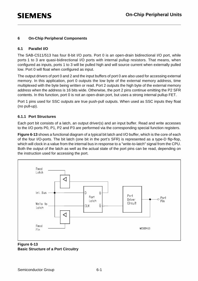
Each port bit consists of a latch, an output driver(s) and an input buffer. Read and write accessesto the I/O ports P0, P1, P2 and P3 are performed via the corresponding special function registers.
Figure 6-13 shows a functional diagram of a typical bit latch and I/O buffer, which is the core of eachof the four I/O-ports. The bit latch (one bit in the port’s SFR) is represented as a type-D flip-flop,which will clock in a value from the internal bus in response to a "write-to-latch" signal from the CPU.Both the output of the latch as well as the actual state of the port pins can be read, depending onthe instruction used for accessing the port.
Figure 6-13Basic Structure of a Port Circuitry
Semiconductor Group 6-1

On-Chip Peripheral Units
Port 1, 2 and 3 output drivers have internal pullup FET’s (see figure 6-6-14). Each I/O line can beused independently as an input or output. To be used as an input, the port bit must contain a one(1) (that means for figure 6-2: Q=0), which turns off the output driver FET n1. Then, for ports 1, 2and 3, the pin is pulled high by the internal pullups, but can be pulled low by an external source.When externally pulled low the port pins source current (IIL or ITL). For this reason these ports aresometimes called "quasi-bidirectional".
Figure 6-14Basic Output Driver Circuit of Ports 1, 2 and 3
Semiconductor Group 6-2

On-Chip Peripheral Units
In fact, the pullups mentioned before and included in figure 6-2 are pullup arrangements shown infigure 6-6-15a. One n-channel pulldown FET and three pullup FETs are used:
Figure 6-15aOutput Driver Circuit of Ports 1, 2 and 3 (except P1.2, P1.3, P1.4 and P1.5)
– The pulldown FET n1 is of n-channel type. It is a very strong driver transistor which is capableof sinking high currents (IOL); it is only activated if a "0" is programmed to the port pin. A shortcircuit to VCC must be avoided if the transistor is turned on, since the high current might destroythe FET. This also means that no ”0“ must be programmed into the latch of a pin that is usedas input.
– The pullup FET p1 is of p-channel type. It is activated for two oscillator periods (S1P1 andS1P2) if a 0-to-1 transition is programmed to the port pin, i.e. a "1" is programmed to the portlatch which contained a "0". The extra pullup can drive a similar current as the pulldown FETn1. This provides a fast transition of the logic levels at the pin.
– The pullup FET p2 is of p-channel type. It is always activated when a "1" is in the port latch,thus providing the logic high output level. This pullup FET sources a much lower current thanp1; therefore the pin may also be tied to ground, e.g. when used as input with logic low inputlevel.
– The pullup FET p3 is of p-channel type. It is only activated if the voltage at the port pin ishigher than approximately 1.0 to 1.5 V. This provides an additional pullup current if a logichigh level shall be output at the pin (and the voltage is not forced lower than approximately1.0 to 1.5 V). However, this transistor is turned off if the pin is driven to a logic low level, e.gwhen used as input. In this configuration only the weak pullup FET p2 is active, which sourcesthe current IIL . If, in addition, the pullup FET p3 is activated, a higher current can be sourced(ITL). Thus, an additional power consumption can be avoided if port pins are used as inputswith a low level applied. However, the driving capability is stronger if a logic high level isoutput.
Semiconductor Group 6-3
On-Chip Peripheral Units
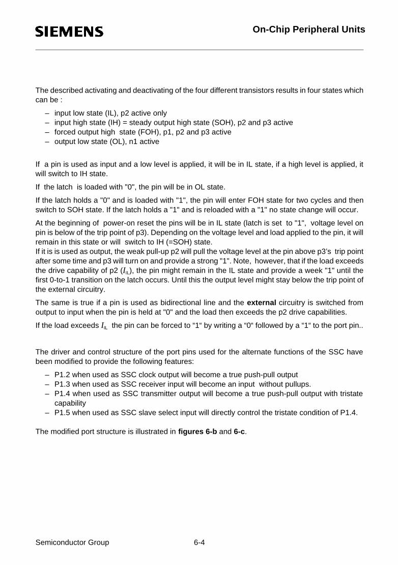
The described activating and deactivating of the four different transistors results in four states whichcan be :
– input low state (IL), p2 active only– input high state (IH) = steady output high state (SOH), p2 and p3 active– forced output high state (FOH), p1, p2 and p3 active – output low state (OL), n1 active
If a pin is used as input and a low level is applied, it will be in IL state, if a high level is applied, itwill switch to IH state.
If the latch is loaded with "0", the pin will be in OL state.
If the latch holds a "0" and is loaded with "1", the pin will enter FOH state for two cycles and thenswitch to SOH state. If the latch holds a "1" and is reloaded with a "1" no state change will occur.
At the beginning of power-on reset the pins will be in IL state (latch is set to "1", voltage level onpin is below of the trip point of p3). Depending on the voltage level and load applied to the pin, it willremain in this state or will switch to IH (=SOH) state. If it is is used as output, the weak pull-up p2 will pull the voltage level at the pin above p3’s trip pointafter some time and p3 will turn on and provide a strong "1". Note, however, that if the load exceedsthe drive capability of p2 (IIL), the pin might remain in the IL state and provide a week "1" until thefirst 0-to-1 transition on the latch occurs. Until this the output level might stay below the trip point ofthe external circuitry.
The same is true if a pin is used as bidirectional line and the external circuitry is switched fromoutput to input when the pin is held at "0" and the load then exceeds the p2 drive capabilities.
If the load exceeds IIL the pin can be forced to “1“ by writing a “0“ followed by a “1“ to the port pin..
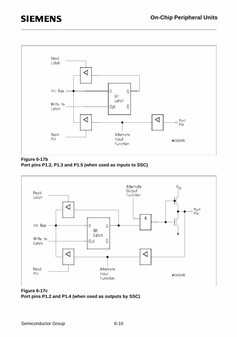
The driver and control structure of the port pins used for the alternate functions of the SSC havebeen modified to provide the following features:
– P1.2 when used as SSC clock output will become a true push-pull output – P1.3 when used as SSC receiver input will become an input without pullups.– P1.4 when used as SSC transmitter output will become a true push-pull output with tristate
capability– P1.5 when used as SSC slave select input will directly control the tristate condition of P1.4.
The modified port structure is illustrated in figures 6-b and 6-c.
Semiconductor Group 6-4

On-Chip Peripheral Units
Figure 6-15bDriver Circuit of Port 1 pins P1.2 and P1.4 (when used for SLCK and STO)
Pin Control for SCLK
When the SSC is disabled, both Enable Push-pull and Tristate will be inactive, the pin behaves likea standard IO pin.
In master mode and with SSC enabled, Enable Push-pull will be active and Tristate will be inactive.
In slave mode and with SSC enabled, Enable Push-pull will be inactive and Tristate will be active.
Pin Control for STO
When the SSC is disabled, both Enable Push-pull and Tristate will be inactive.
In master mode and SSC enabled, Enable Push-pull will be active and Tristate will be inactive.
In slave mode and SSC enabled, Enable Push-pull will be active. If the transmitter is enabled (SLS and TEN active), Tristate will be inactive.If the transmitter is disabled (either SLS or TEN inactive), Tristate will be active.
Semiconductor Group 6-5

On-Chip Peripheral Units
Figure 6-15cDriver Circuit of Port 1 pins P1.3 and P1.5 (when used for SRI and SLS)
When enabling the SSC, inputs used for the SSC will be switched into a high-impedance mode.
For P1.3/SRI, Tristate will be enabled, when the SSC is enabled.
For P1.5/SLS, Tristate will be enabled, when the SSC is enabled and is switched to slave mode. Inmaster mode this pin will remain a regular I/O pin.
Semiconductor Group 6-6

On-Chip Peripheral Units
Port 0, in contrast to ports 1, 2 and 3, is considered as "true" bidirectional, because the port 0 pinsfloat when configured as inputs. Thus, this port differs in not having internal pullups. The pullup FETin the P0 output driver (see figure 6-16a) is used only when the port is emitting 1 s during theexternal memory accesses. Otherwise, the pullup is always off. Consequently, P0 lines that areused as output port lines are open drain lines. Writing a "1" to the port latch leaves both output FETsoff and the pin floats. In that condition it can be used as high-impedance input. If port 0 is configuredas general I/O port and has to emit logic high-level (1), external pullups are required.
Figure 6-16aPort 0 Circuitry
Semiconductor Group 6-7

On-Chip Peripheral Units
6.1.2 Port 0 and Port 2 used as Address/Data Bus
As shown in figure 6-16a and below in figure 6-16b , the output drivers of ports 0 and 2 can beswitched to an internal address or address/data bus for use in external memory accesses. In thisapplication they cannot be used as general purpose I/O, even if not all address lines are usedexternally. The switching is done by an internal control signal dependent on the input level at theEA pin and/or the contents of the program counter. If the ports are configured as an address/databus, the port latches are disconnected from the driver circuit. During this time, the P2 SFR remainsunchanged while the P0 SFR has 1’s written to it. Being an address/data bus, port 0 uses a pullupFET as shown in figure 6-16a . When a 16-bit address is used, port 2 uses the additional strongpullups p1 to emit 1’s for the entire external memory cycle instead of the weak ones (p2 and p3)used during normal port activity.
Figure 6-16bPort 2 Circuitry
MCS02123
D
CLK
BitLatch
Q
Q
ControlAddr.
MUX
InternalPull UpArrangement
VCC
PortPin
Int. Bus
Write to
PinRead
Latch
LatchRead
=1
Semiconductor Group 6-8

On-Chip Peripheral Units
6.1.3 Alternate Functions
The pins of ports 1 and 3 are multifunctional. They are port pins and also serve to implementalternate functions (special inputs/outputs for on-chip peripherals) as listed in table 6-6-3.
Figure 6-17a shows a functional diagram of a port latch with alternate function. To pass thealternate function to the output pin and vice versa, however, the gate between the latch and drivercircuit must be open. Thus, to use the alternate input or output functions, the corresponding bit latchin the port SFR has to contain a one (1); otherwise the pulldown FET is on and the port pin is stuckat 0. After reset all port latches contain ones (1).
Figure 6-17aPorts 1 and 3
For port pins P1.2 to P1.5 different structures apply, see figures 6-17b and 6-17c.
MCS01827
D
CLK
BitLatch
Q
Q
InternalPull UpArrangement
Pin
ReadLatch
toLatch
ReadPin
Write
VCC
Int. Bus
AlternateOutput
Function
AlternateInput
Function
&
Semiconductor Group 6-9
On-Chip Peripheral Units
Figure 6-17bPort pins P1.2, P1.3 and P1.5 (when used as inputs to SSC)
Figure 6-17cPort pins P1.2 and P1.4 (when used as outputs by SSC)
Semiconductor Group 6-10

On-Chip Peripheral Units
Ports 1 and 3 provide several alternate functions as listed in table 6-3:
Table 6-3Alternate Functions of Port 1 and 3
Port Symbol Function
P1.0P1.1
P1.2P1.3P1.4P1.5P3.0
P3.1
P3.2P3.3P3.4P3.5P3.6P3.7
T2T2EX
SCLKSRISTOSLSRXD
TXD
INT0INT1T0T1WRRD
Input to counter 2 (SAB-C513/513A/C513A-H only)Capture-reload trigger of timer 2 / up-down count (SAB-C513/513A/C513A-H only)SSC master clock output, slave clock inputSSC serial data inSSC serial data outSSC slave selectSerial port’s receiver data input (asynchronous) or data input/output (synchronous, not available at SAB-C511/C511A)Serial port’s transmitter data output (asynchronous) or data clock output (synchronous, not available at SAB-C511/C511A)External interrupt 0 input, timer 0 gate controlExternal interrupt 1 input, timer 1 gate controlTimer 0 external counter inputTimer 1 external counter inputExternal data memory write strobeExternal data memory read strobe
Semiconductor Group 6-11

On-Chip Peripheral Units
6.1.4 Port Handling
6.1.4.1 Port Timing
When executing an instruction that changes the value of a port latch, the new value arrives at thelatch during S6P2 of the final cycle of the instruction. However, port latches are only sampled bytheir output buffers during phase 1 of any clock period (during phase 2 the output buffer holds thevalue it noticed during the previous phase 1). Consequently, the new value in the port latch will notappear at the output pin until the next phase 1, which will be at S1P1 of the next machine cycle.
When an instruction reads a value from a port pin (e.g. MOV A, P1) the port pin is actually sampledin state 5 phase 1 or phase 2 depending on port and alternate functions. Figure 6-18 illustrates thisport timing. It must be noted that this mechanism of sampling once per machine cycle is also usedif a port pin is to detect an "edge", e.g. when used as counter input. In this case an "edge" isdetected when the sampled value differs from the value that was sampled the cycle before.Therefore, there must be met certain requirements on the pulse length of signals in order to avoidsignal "edges" not being detected. The minimum time period of high and low level is one machinecycle, which guarantees that this logic level is noticed by the port at least once.
Figure 6-18Port Timing
Semiconductor Group 6-12

On-Chip Peripheral Units
6.1.4.2 Port Loading and Interfacing
The output buffers of ports 1, 2 and 3 can drive TTL inputs directly. The maximum port load whichstill guarantees correct logic output levels can be be seen in the Data Sheet of the SAB-C511/513family members. The corresponding DC parameters are VOL and VOH.
The same applies to port 0 output buffers. They do, however, require external pullups to drivefloating inputs, except when being used as the address/data bus.
When used as inputs it must be noted that the ports 1, 2 and 3 are not floating but have internalpullup transistors. The driving devices must be capable of sinking a sufficient current if a logic lowlevel shall be applied to the port pin (the parameters ITL and IIL in the DC characteristics specifythese currents). Port 0 has floating inputs when used for digital input.
6.1.4.3 Read-Modify-Write Feature of Ports 1, 2 and 3
Some port-reading instructions read the latch and others read the pin (see figure 6-13). Theinstructions reading the latch rather than the pin read a value, possibly change it, and then rewriteit to the latch. These are called "read-modify-write"- instructions, which are listed in table 6-4. If thedestination is a port or a port pin, these instructions read the latch rather than the pin. Note that allother instructions which can be used to read a port, exclusively read the port pin. In any case,reading from latch or pin, resp., is performed by reading the SFR P0, P1, P2 and P3; for example,"MOV A, P1" reads the value from port 3 pins, while "ANL P1, #0AAH" reads from the latch, modifiesthe value and writes it back to the latch.
It is not obvious that the last three instructions in table 6-4 are read-modify-write instructions, butthey are. The reason is that they read the port byte, all 8 bits, modify the addressed bit, then writethe complete byte back to the latch.
Table 6-4"Read-Modify-Write"-Instructions
Instruction Function
ANL Logic AND; e.g. ANL P1, A
ORL Logic OR; e.g. ORL P2, A
XRL Logic exclusive OR; e.g. XRL P3, A
JBC Jump if bit is set and clear bit; e.g. JBC P1.1, LABEL
CPL Complement bit; e.g. CPL P3.0
INC Increment byte; e.g. INC P1
DEC Decrement byte; e.g. DEC P1
DJNZ Decrement and jump if not zero; e.g. DJNZ P3, LABEL
MOV Px.y,C Move carry bit to bit y of port x
CLR Px.y Clear bit y of port x
SETB Px.y Set bit y of port x
Semiconductor Group 6-13

On-Chip Peripheral Units
The reason why read-modify-write instructions are directed to the latch rather than the pin is to avoida possible misinterpretation of the voltage level at the pin. For example, a port bit might be used todrive the base of a transistor. When a "1" is written to the bit, the transistor is turned on. If the CPUthen reads the same port bit at the pin rather than the latch, it will read the base voltage of thetransistor (approx. 0.7 V, i.e. a logic low level!) and interpret it as "0". For example, when modifyinga port bit by a SETB or CLR instruction, another bit in this port with the above mentionedconfiguration might be changed if the value read from the pin were written back to the latch.However, reading the latch rater than the pin will return the correct value of "1".
Semiconductor Group 6-14

On-Chip Peripheral Units
6.2 Timers/Counters
The SAB-C511/513 microcontrollers contains two (SAB-C511/C511A) or three (SAB-C513/C513A/C513A-H) 16-bit timers/counters which are useful in many applications for timing and countingfunctions.
In timer function, the register is incremented every machine cycle. Thus one can think of it ascounting machine cycles. Since a machine cycle consists of 12 oscillator periods, the counter rateis 1/12 of the oscillator frequency.
In counter function, the register is incremented in response to a 1-to-0 transition (falling edge) atits corresponding external input pin, T0 or T1 (alternate functions of P3.4 and P3.5, resp.). In thisfunction the external input is sampled during S5P2 of every machine cycle. When the samples showa high in one cycle and a low in the next cycle, the counter is incremented. The new count valueappears in the register during S3P1 of the cycle following the one in which the transition wasdetected. Since it takes two machine cycles (24 oscillator periods) to recognize a 1-to-0 transition,the maximum count rate is 1/24 of the oscillator frequency. There are no restrictions on the dutycycle of the external input signal, but to ensure that a given level is sampled at least once before itchanges, it must be held for at least one full machine cycle.
Semiconductor Group 6-15

On-Chip Peripheral Units
6.2.1 Timer/Counter 0 and 1
Timer / counter 0 and 1 of the SAB-C511/513 family components are fully compatible with timer /counter 0 and 1 of the 8051 microcontroller and can be used in the same four operating modes:
Mode 0: 8-bit timer/counter with a divide-by-32 prescaler
Mode 1: 16-bit timer/counter
Mode 2: 8-bit timer/counter with 8-bit auto-reload
Mode 3: Timer/counter 0 is split into one 8-bit timer/counter and one 8-bit timer when programmedto this mode. Timer/counter 1 set to this mode will simply hold its count. The effect is thesame as setting TR1 = 0, disabling the counter.
The external inputs INT0 and INT1 can be programmed to function as a gate for timer/counters 0and 1 to facilitate pulse width measurements.
Each timer consists of two 8-bit registers (TH0 and TL0 for timer/counter 0, TH1 and TL1 for timer/counter 1) which may be combined to one timer configuration depending on the mode that isestablished. The functions of the timers are controlled by two special function registers TCON andTMOD.
In the following descriptions the symbols TH0 and TL0 are used to specify the high-byte and thelow-byte of timer 0 (TH1 and TL1 for timer 1, respectively). The operating modes are described andshown for timer 0. If not explicity noted, this applies also to timer 1.
Special Function Register TCON (Address 88H) Reset Value : 00H
Bit Function
TR0 Timer 0 run control bit.Set/cleared by software to turn timer/counter 0 ON/OFF.
TF0 Timer 0 overflow flag. Set by hardware on timer/counter overflow.Cleared by hardware when processor vectors to interrupt routine.
TR1 Timer 1 run control bit.Set/cleared by software to turn timer/counter 1 ON/OFF.
TF1 Timer 1 overflow flag. Set by hardware on timer/counter overflow.Cleared by hardware when processor vectors to interrupt routine.
TF1 TR1 TF0 TR088H TCON
Bit No. 7 6 5 4 3 2 1 0MSB LSB
IE1 IT1 IE0 IT0
These bits are not used in controlling timer/counter 0 and 1.
Semiconductor Group 6-16

On-Chip Peripheral Units
Special Function Register TMOD (Address 89H) Reset Value : 00H
Bit Function
Gate Gating control.When set, timer/counter "x" is enabled only while "INTx" pin is high and "TRx" control bit is set.When cleared timer "x" is enabled whenever "TRx" control bit is set.
C/T Counter or timer select bit.Set for counter operation (input from "Tx" input pin).Cleared for timer operation (input from internal system clock).
M1 M00 0
Timer modes select bits8-bit timer/counter."THx" operates as 8-bit timer/counter"TLx" serves as 5-bit prescaler.
0 1 16-bit timer/counter."THx" and "TLx" are cascaded; there is no prescaler.
1 0 8-bit auto-reload timer/counter."THx" holds a value which is to be reloaded into "TLx" each time it overflows.
1 1 Timer 0:TL0 is an 8-bit timer/counter controlled by the standard timer 0 control bits. TH0 is an 8-bit timer only controlled by timer 1 control bits.
1 1 Timer 1:Timer/counter 1 stops
Gate C/T M1 M089H TMOD
Bit No. 7 6 5 4 3 2 1 0MSB LSB
Gate C/T M1 M0
Timer 1 Control Timer 0 Control
Semiconductor Group 6-17

On-Chip Peripheral Units
6.2.1.1 Mode 0
Putting either timer/counter 0,1 into mode 0 configures it as an 8-bit timer/counter with a divide-by-32 prescaler. Figure 6-19 shows the mode 0 operation.
In this mode, the timer register is configured as a 13-bit register. As the count rolls over from all 1’sto all 0’s, it sets the timer overflow flag TF0. The overflow flag TF0 then can be used to request aninterrupt. The counted input is enabled to the timer when TR0 = 1 and either Gate = 0 or INT0 = 1(setting Gate = 1 allows the timer to be controlled by external input INT0, to facilitate pulse widthmeasurements). TR0 is a control bit in the special function register TCON; Gate is in TMOD.
The 13-bit register consists of all 8 bits of TH0 and the lower 5 bits of TL0. The upper 3 bits of TL0are indeterminate and should be ignored. Setting the run flag (TR0) does not clear the registers.
Mode 0 operation is the same for timer 0 as for timer 1. Substitute TR0, TF0, TH0, TL0 and INT0for the corresponding timer 1 signals in figure 6-19. There are two different gate bits, one for timer1 (TMOD.7) and one for timer 0 (TMOD.3).
Figure 6-19Timer/Counter 0, Mode 0: 13-Bit Timer/Counter
MCS02143
1
&
OSC
C/T = 0TL0 TH0 TF0
C/T = 1(8 Bits)
TR0Gate
P3.2/INTO
Control
Interrupt
P3.4/T0
(5 Bits)
÷ 12
_<
=1
Semiconductor Group 6-18

On-Chip Peripheral Units
6.2.1.2 Mode 1
Mode 1 is the same as mode 0, except that the timer register is running with all 16 bits. Mode 1 isshown in figure 6-20.
Figure 6-20Timer/Counter 0, Mode 1: 16-Bit Timer/Counter
MCS02095
1
&
OSC
C/T = 0TL0 TH0 TF0
C/T = 1
(8 Bits)
TR0Gate
P3.2/INTO
Control
Interrupt
P3.4/T0
(8 Bits)
_<
÷ 12
=1
Semiconductor Group 6-19

On-Chip Peripheral Units
6.2.1.3 Mode 2
Mode 2 configures the timer register as an 8-bit counter (TL0) with automatic reload, as shown infigure 6-21. Overflow from TL0 not only sets TF0, but also reloads TL0 with the contents of TH0,which is preset by software. The reload leaves TH0 unchanged.
Mode 2 operation is the same for timer 0 as for timer 1. Substitute TR0, TF0, TH0, TL0 and INT0for the corresponding timer 1 signals in figure 6-21. There are two different gate bits, one for timer1 (TMOD.7) and one for timer 0 (TMOD.3).
Figure 6-21Timer/Counter 0, Mode 2: 8-Bit Timer/Counter with Auto-Reload
Semiconductor Group 6-20

On-Chip Peripheral Units
6.2.1.4 Mode 3
Mode 3 has different effects on timer 0 and timer 1. Timer 1 in mode 3 simply holds its count andstops counting. The effect is the same as setting TR1=0. Timer 0 in mode 3 establishes TL0 andTH0 as two seperate counters. The logic for mode 3 on timer 0 is shown in figure 6-22. TL0 usesthe timer 0 control bits: C/T, Gate, TR0, INT0 and TF0. TH0 is locked into a timer function (countingmachine cycles) and takes over the use of TR1 and TF1 from timer 1. Thus, TH0 now controls the"timer 1" interrupt.
Mode 3 is provided for applications requiring an extra 8-bit timer or counter. When timer 0 is inmode 3, timer 1 can be turned on and off by switching it out of and into its own mode 3, or can stillbe used by the serial channel as a baud rate generator, or in fact, in any application not requiringan interrupt from timer 1 itself.
Figure 6-22Timer/Counter 0, Mode 3: Two 8-Bit Timers/Counters
MCS02096
1
&
OSC
C/T = 0TL0 TF0
C/T = 1
(8 Bits)
TR1Gate
P3.2/INT0
Control
Interrupt
(8 Bits)
TH0Interrupt
TF1
ControlTR1
/12f OSC
OSCf /12
P3.4/T0
÷ 12
=1
<_
Semiconductor Group 6-21

On-Chip Peripheral Units
6.2.2 Timer/Counter 2 (SAB-C513/C513A/C513A-H only)
Timer 2 is a 16-bit timer / counter which can operate as timer or counter. It has 3 operating modes :
– 16-bit auto-reload mode (up or down counting)– 16-bit capture mode– Baudrate generator (see chapter 6.3.3.2)
The modes are selected by bits in the SFR T2CON (C8H) as shown in table 6-5.
Table 6-5Timer/Counter 2 - Operating Modes
Timer 2 consists of two 8-bit registers, TH2 and TL2. In the timer function, the TL2 register isincremented every machine cycle. Since a machine cycle consists of 12 oscillator periods, the countrate is 1/12 of the oscillator frequency.
In the counter function, the register is incremented in response to a 1-to-0 transition at itscorresponding external input pin T2 (P1.0). In this function, the external input is sampled duringS5P2 of every machine cycle. When the samples show a high in one cycle and a low in the nextcycle, the count is incremented. The new value appears in the register during S3P1 of the cyclefollowing the one in which the transition was detected. Since it takes two machine cycles torecognize a 1-to-0 transition, the maximum count rate is 1/24 of the oscilllator frequency. To ensurethat a given level is sampled at least once before it changes, it should be held for at least one fullmachine cycle.
RCLK + TCLK CP/RL2 TR2 Mode
0 0 1 16-bit auto-reload
0 1 1 16-bit capture
1 X 1 Baud rate generator
X X 0 (OFF)
Semiconductor Group 6-22

On-Chip Peripheral Units
Special Function Register T2CON (Address C8H) Reset Value : 00H
Bit Function
TF2 Timer 2 Overflow Flag.Set by a timer 2 overflow. Must be cleared by software. TF2 will not be set when either RCLK = 1 or TCLK = 1.
EXF2 Timer 2 External Flag.Set when either a capture or reload is caused by a negative transition on T2EX and EXEN2 = 1. When timer 2 interrupt is enabled, EXF2 = 1 will cause the CPU to vector to the timer 2 interrupt routine. EXF2 must be cleared by software. EXF2 does not cause an interrupt in up/down counter mode (DCEN = 1, SFR T2MOD)
RCLK Receive Clock Enable.When set, causes the serial port to use timer 2 overflow pulses for its receive clock in serial port modes 1 and 3. RCLK = 0 causes timer 1 overflows to be used for the receive clock.
TCLK Transmit Clock Enable.When set, causes the serial port to use timer 2 overflow pulses for its transmit clock in serial port modes 1 and 3. TCLK = 0 causes timer 1 overflow to be used for the transmit clock.
EXEN2 Timer 2 External Enable.When set, allows a capture or reload to occur as a result of a negative transition on pin T2EX (P1.1) if timer 2 is not being used to clock the serial port. EXEN2 = 0 causes timer 2 to ignore events at T2EX.
TR2 Start / Stop Control for Timer 2.TR2 = 1 starts timer 2.
C/T2 Timer or Counter Select for Timer 2.C/T2 = 0 for timer function. C/T2 = 1 for external event counter (falling edge triggered).
CP/RL2 Capture / Reload Select.CP/RL2 = 1 causes captures to occur an negative transitions at pin T2EX if EXEN2 = 1. CP/RL2 = 0 causes automatic reloads to occur when timer 2 overflows or negative transitions occur at pin T2EX when EXEN2 = 1. When either RCLK = 1 or TCLK = 1, this bit is ignored and the timer is forced to auto-reload on timer 2 overflow.
TF2 EXF2 RCLK TCLKC8H T2CON
Bit No. 7 6 5 4 3 2 1 0MSB LSB
EXEN2 TR2 C/T2 CP/RL2
Semiconductor Group 6-23

On-Chip Peripheral Units
6.2.2.1 Auto-Reload Mode (Up or Down Counter)
Timer 2 can be programmed to count up or down when configured in its 16-bit auto-reload mode.This feature is invoked by a bit named DCEN (Down Counter Enable), which is located in SFRT2MOD. When DCEN is set, timer 2 can count up or down depending on the value of pin T2EX(P1.1).
Special Function Register T2MOD (Address C9H) Reset Value : XXXXXXX0B
Figure 6-23 shows timer 2 automatically counting up when DCEN=0. In this mode there are twooptions selectable by bit EXEN2 in SFR T2CON.
Figure 6-23Timer 2 Auto-Reload Mode (DCEN = 0)
Bit Function
– Not implemented, reserved for future use.
DCEN When set, this bit allows timer 2 to be configured as an up/down counter. With T2EX=0 down-counting is selected, with DCEN=1 up-counting is enabled.
– – – –C9H T2MOD
Bit No. 7 6 5 4 3 2 1 0MSB LSB
– – – DCEN
Semiconductor Group 6-24

On-Chip Peripheral Units
If EXEN2 = 0, timer 2 counts up to FFFFH and then sets the TF2 bit upon overflow. The overflowalso causes the timer registers to be reloaded with the 16-bit value in RC2H and RC2L. The valuesin RC2H and RC2L are preset by software.
If EXEN2 = 1, a 16-bit reload can be triggered either by an overflow or by a 1-to-0 transition at theexternal input T2EX (P1.1). This transition also sets the EXF2 bit. Both the TF2 and EXF2 bits cangenerate an timer 2 interrupt if enabled.
Setting the DCEN bit enables timer 2 to count up or down as shown in figure 6-24. In this mode theT2EX pin controls the direction of count.
Figure 6-24Timer 2 Auto-Reload Mode (DCEN = 1)
A logic 1 at T2EX makes timer 2 count up. The timer will overflow at FFFFH and set the TF2 bit.This overflow also causes the 16-bit value in RC2H and RC2L to be reloaded into the timerregisters, TH2 and TL2, respectively.
A logic 0 at T2EX makes timer 2 count down. Now the timer underflows when TH2 and TL2 equalthe values stored in RC2H and RC2L. The underflow sets the TF2 bit and causes FFFFH to bereloaded into the timer registers. The EXF2 bit toggles whenever timer 2 overflows or underflows.This bit can be used as a 17th bit of resolution if desired. In this operating mode, EXF2 does notflag an interrupt.
Semiconductor Group 6-25

On-Chip Peripheral Units
Note: P1.1/T2EX is sampled during S5P2 of every machine cycle. The next increment/decrementof timer 2 will be done during S3P1 in the next cycle.
6.2.2.2 Capture Mode
In the capture mode there are two options selected by bit EXEN2 in SFR T2CON.
If EXEN2 = 0, timer 2 is a 16-bit timer or counter which upon overflow sets bit TF2 in SFR T2CON.This bit can be used to generate an interrupt.
If EXEN2 = 1, timer 2 still does the above, but with added feature that a 1-to-0 transition at externalinput T2EX causes the current value in TH2 and TL2 to be captured into RC2H and RC2L,respectively. In addition, the transition at T2EX causes bit EXF2 in SFR T2CON to be set. The EXF2bit, like TF2, can generate an interrupt. The capture mode is illustrated in figure 6-25.
Figure 6-25Timer 2 in Capture Mode
The baud rate generator mode is selected by RCLK = 1 and/or TCLK = 1 in SFR T2CON. It will bedescribed in conjunction with the serial port.
Semiconductor Group 6-26

On-Chip Peripheral Units
6.3 General Purpose Serial Interface USART (SAB-C513/C513AC513A-H only)
The serial port is full duplex, meaning it can transmit and receive simultaneously. It is also receive-buffered, meaning it can commence reception of a second byte before a previously received bytehas been read from the receive register. However, if the first byte still hasn’t been read by the timereception of the second byte is complete, the first byte will be lost. The serial port receive andtransmit registers are both accessed at special function register SBUF. Writing to SBUF loads thetransmit register, and reading SBUF accesses a physically separate receive register.
The serial port can operate in 4 modes (one synchronous mode, three asynchronous modes):
Mode 0, Shift Register (Synchronous) Mode:
Serial data enters and exits through RXD. TXD outputs the shift clock. 8 data bits are transmitted/received (LSB first). The baud rate is fixed at 1/12 of the oscillator frequency. See section 6.3.4 formore detailed information.
Mode 1, 8-Bit USART, Variable Baud Rate:
10 bits are transmitted (through TXD) or received (through RXD): a start bit (0), 8 data bits (LSBfirst), and a stop bit (1). On receive, the stop bit goes into RB8 in special function register SCON.The baud rate is variable. See section 6.3.5 for more detailed information.
Mode 2, 9-Bit USART, Fixed Baud Rate:
11 bits are transmitted (through TXD) or received (through RXD): a start bit (0), 8 data bits (LSBfirst), a programmable 9th data bit, and a stop bit (1). On transmit, the 9th data bit (TB8 in SCON)can be assigned to the value of 0 or 1. Or, for example, the parity bit (P, in the PSW) could be movedinto TB8. On receive, the 9th data bit goes into RB8 in special function register SCON, while thestop bit is ignored. The baud rate is programmable to either 1/32 or 1/64 of the oscillator frequency.See section 6.3.6 for more detailed information.
Mode 3, 9-Bit USART, Variable Baud Rate:
11 bits are transmitted (through TXD) or received (through RXD): a start bit (0), 8 data bits (LSBfirst), a programmable 9th data bit, and a stop bit (1). In fact, mode 3 is the same as mode 2 in allrespects except the baud rate. The baud rate in mode 3 is variable. See section 6.3.6 for moredetailed information.
In all four modes, transmission is initiated by any instruction that uses SBUF as a destinationregister. Reception is initiated in mode 0 by the condition RI = 0 and REN = 1. Reception is initiatedin the other modes by the incomming start bit if REN = 1.
Semiconductor Group 6-27

On-Chip Peripheral Units
6.3.1 Multiprocessor Communications
Modes 2 and 3 have a special provision for multiprocessor communications. In these modes, 9 databits are received. The 9th data bit goes into RB8. Then comes a stop bit. The port can beprogrammed such that when the stop bit is received, the serial port interrupt will be activated onlyif RB8 = 1. This feature is enabled by setting bit SM2 in SCON. A way to use this feature inmultiprocessor systems is as follows.
When the master processor wants to transmit a block of data to one of several slaves, it first sendsout an address byte which identifies the target slave. An address byte differs from a data byte inthat the 9th bit is 1 in an address byte and 0 in a data byte. With SM2 = 1, no slave will be interruptedby a data byte. An address byte, however, will interrupt all slaves, so that each slave can examinethe received byte and see if it is beeing addressed. The addressed slave will clear its SM2 bit andprepare to receive the data bytes that will be coming. The slaves that weren’t being addressed leavetheir SM2s set and go on about their business, ignoring the incoming data bytes.
SM2 has no effect in mode 0, and in mode 1 can be used to check the validity of the stop bit. In amode 1 reception, if SM2 = 1, the receive interrupt will not be activated unless a valid stop bit isreceived.
Semiconductor Group 6-28

On-Chip Peripheral Units
6.3.2 Serial Port Control Register
The serial port control and status register is the special function register SCON. This registercontains not only the mode selection bits, but also the 9th data bit for transmit and receive (TB8 andRB8) and the serial port interrupt bits (TI and RI).
Special Function Register SCON (Address 98H) Reset Value : 00H
Bit Function
SM0 SM10 00 11 01 1
Serial Mode Select BitsSerial mode 0: Shift register, fixed baud rate (fOSC/12)Serial mode 1: 8-bit UART, variable baud rateSerial mode 2: 9-bit UART, fixed baud rate (fOSC/64 or fOSC/32)Serial mode 3: 9-bit UART, variable baud rate
SM2 Multiprocessor Communication SelectEnables the multiprocessor communication feature in modes 2 and 3. In mode 2 or 3, if SM2 is set to 1 then RI will not be activated if the received 9th data bit (RB8) is 0. In mode 1, if SM2 = 1 then RI will not be activated if a valid stop bit was not received. In mode 0, SM2 should be 0.
REN Receiver Enable Enables serial reception. Set by software to enable reception. Clear by software to disable reception.
TB8 Transmit Bit 8Is the 9th data bit that will be transmitted in modes 2 and 3. Set or clear by software as desired.
RB8 Receive Bit 8In modes 2 and 3, is the 9th data bit that was received. In mode 1, if SM2 = 0, RB8 is the stop bit that was received. In mode 0, RB8 is not used.
TI Transmit Interrupt FlagIs transmit interupt flag. Set by hardware at the end of the 8th bit time in mode 0, or at the beginning of the stop bit in the other modes, in any serial transmission. Must be cleared by software.
RI Receive Interrupt FlagIs receive interrupt flag. Set by hardware at the end of the 8th bit time in mode 0, or halfway through the stop bit time in the other modes, in any serial reception (except see SM2). Must be cleared by software.
SM0 SM1 SM2 REN98H SCON
Bit No. 7 6 5 4 3 2 1 0MSB LSB
TB8 RB8 TI RI
Semiconductor Group 6-29

On-Chip Peripheral Units
6.3.3 Baud Rates
There are several possibilities to generate the baud rate clock for the serial interface depending onthe mode in which it is operated.
To clearify the terminology, something should be mentioned about the differences between "baudrate clock" and "baud rate".
The serial interface requires a clock rate which is 16 times the baud rate for the internalsynchronization. Therefore, the baud rate generators have to provide a "baud rate clock" to theserial interface which - there divided by 16 - results in the actual "baud rate".
However, all formulas given in the following chapter already includes the factor and calculate thefinal baud rate.
Mode 0
The baud rate in mode 0 is fixed:
Mode 0 baud rate = oscillator frequency/12 = fOSC/12
Mode 2
The baud rate in mode 2 depends on the value of bit SMOD in special function register PCON(87H). If SMOD = 0 (which is the value on reset), the baud rate is fOSC/64. If SMOD = 1, the baudrate is fOSC/32.
Mode 2 baud rate = 2SMOD/64×(fOSC)
Modes 1 and 3
The baud rates in mode 1 and 3 are determined by the timer overflow rate. These baud rates canbe determined by timer 1 or by timer 2 or by both (one for transmit and the other for receive).
Semiconductor Group 6-30

On-Chip Peripheral Units
6.3.3.1 Using Timer 1 to Generate Baud Rates
When timer 1 is used as the baud rate generator, the baud rates in modes 1 and 3 are determinedby the timer 1 overflow rate and the value of SMOD as follows:
Modes 1,3 baud rate = 2SMOD/32×(timer 1 overflow rate)
The timer 1 interrupt should be disabled in this application. The timer itself can be configured foreither "timer" or "counter" operation, and in any of its 3 running modes. In the most typicalapplications, it is configured for "timer" operation, in the auto-reload mode (high nibble ofTMOD=0010B). In that case, the baud rate is given by the formula
Modes 1,3 baud rate = (2SMOD/32) × (fOSC/(12×(256–TH1)))
One can achieve very low baud rates with timer 1 by leaving the timer 1 interrupt enabled, andconfiguring the timer to run as a 16-bit timer (high nibble of TMOD = 0001B), and using the timer 1interrupt to do a 16-bit software reload.
Table 6-7 lists commonly used baud rates and how they can be obtained from timer 1.
Table 6-7Timer 1 Generated Commonly Used Baud Rates
Baud Rate fOSC SMOD Timer 1
C/T Mode Reload Value
Mode 0 max: 640 kHzMode 2 max: 240 KModes 1, 3: 40 K19.2 K9.6 K4.8 K2.4 K1.2 K
Mode 0 max : 1 MHzMode 2 max : 375 KMode 1,3 : 62.5 K19,2 K9.6 K4.8 K2.4 K1.2 K110110
7.68 MHz7.68 MHz7.68 MHz7.68 MHz7.68 MHz7.68 MHz7.68 MHz7.68 MHz
12 MHz12 MHz12 MHz11.059 MHz11.059 MHz11.059 MHz11.059 MHz11.059 MHz6 MHz12 MHz
X1100000
X111000000
XX000000
XX00000000
XX222222
XX22222221
XXFFHFFHFEHFCHF8HEAH
XXFFHFDHFDHFAHF4HE8H72HFEEBH
Semiconductor Group 6-31

On-Chip Peripheral Units
6.3.3.2 Using Timer 2 to Generate Baud Rates
Timer 2 is selected as the baud rate generator by setting TCLK and/or RCLK in T2CON. Note thenthe baud rates for transmit and receive can be simultaneously different. Setting RCLK and/or TCLKputs timer 2 into its baud rate generator mode, as shown in figure 6-6-26.
Figure 6-26Timer 2 in Baud Rate Generator Mode
The baud rate generator mode is similar to the auto-reload mode, in that rollover in TH2 causes thetimer 2 registers to be reloaded with the 16-bit value in registers RC2H and RC2L, which are presetby software.
Semiconductor Group 6-32

On-Chip Peripheral Units
Now the baud rates in modes 1 and 3 are determined by timer 2’s overflow rate as follows:
Modes 1, 3 baud rate = timer 2 overflow rate/16
The timer can be configured for either "timer" or "counter" operation: In the most typical applications,it is configured for "timer" operation (C/T2 = 0). "Timer" operation is a little different for timer 2 whenit’s being used as a baud rate generator. Normally, as a timer it would increment every machinecycle (thus at fOSC/12). As a baud rate generator, however, it increments every state time (fOSC/2). Inthat case the baud rate is given by the formula :
Modes 1,3 baud rate = fOSC/32×[65536 – (RC2H, RC2L)]
where (RC2H, RC2L) is the content of RC2H and RC2L taken as a 16-bit unsigned integer.
Note that the rollover in TH2 does not set TF2, and will not generate an interrupt. Therefore, thetimer 2 interrupt does not have to be disabled when timer 2 is in the baud rate generator mode. Notetoo, that if EXEN2 is set, a 1-to-0 transition in T2EX can be used as an extra external interrupt, ifdesired.
It should be noted that when timer 2 is running (TR2 = 1) in "timer" function in the baud rategenerator mode, one should not try to read or write TH2 or TL2. Under these conditions the timeris being incremented every state time, and the results of a read or write may not be accurate. TheRC2H/RC2L registers may be read, but shouldn’t be written to, because a write might overlap areload and cause write and/or reload errors. Turn the timer off (clear TR2) before accessing thetimer 2 or RC2H/RC2L registers, in this case.
Semiconductor Group 6-33

On-Chip Peripheral Units
6.3.4 Details about Mode 0
Serial data enters and exists through RXD. TXD outputs the shift clock. 8 data bits are transmitted/received: (LSB first). The baud rate is fixed at fOSC/12.
Figure 6-15a shows a simplyfied functional diagram of the serial port in mode 0. The associatedtiming is illustrated in figure 6-b.
Transmission is initiated by any instruction that uses SBUF as a destination register. The "WRITEto SBUF" signal at S6P2 also loads a 1 into the 9th position of the transmit shift register and tellsthe TX control block to commence a transmission. The internal timing is such that one full machinecycle will elapse between "WRITE to SBUF", and activation of SEND.
SEND enables the output of the shift register to the alternate output function line of P3.0, and alsoenables SHIFT CLOCK to the alternate output function line of P3.1. SHIFT CLOCK is low duringS3, S4, and S5 of every machine cycle, and high during S6, S1 and S2. At S6P2 of every machinecycle in which SEND is active, the contents of the transmit shift register are shifted to the right oneposition.
As data bits shift out to the right, zeroes come in from the left. When the MSB of the data byte is atthe output position of the shift register, then the 1 that was initialy loaded into the 9th position, is justto the left of the MSB, and all positions to the left of that contain zeroes. This condition flags the TXcontrol block to do one last shift and then deactivate SEND and set TI. Both of these actions occurat S1P1 of the 10th machine cycle after "WRITE to SBUF".
Reception is initiated by the condition REN = 1 and R1 = 0. At S6P2 of the next machine cycle, theRX control unit writes the bits 1111 1110 to the receive shift register, and in the next clock phaseactivates RECEIVE.
RECEIVE enables SHIFT CLOCK to the alternate output function line of P3.1. SHIFT CLOCKmakes transitions at S3P1 and S6P1 of every machine cycle. At S6P2 of every machine cycle inwhich RECEIVE is active, the contents of the receive shift register are shifted to the left one position.The value that comes in from the right is the value that was sampled at the P3.0 pin at S5P2 of thesame machine cycle.
As data bit comes in from the right, 1s shift out to the left. When the 0 that was initially loaded intothe rightmost position arrives at the leftmost position in the shift register, it flags the RX control blockto do one last shift and load SBUF. At S1P1 of the 10th machine cycle after the write to SCON thatcleared RI, RECEIVE is cleared and RI is set.
Semiconductor Group 6-34

On-Chip Peripheral Units
Figure 6-27aSerial Interface, Mode 0, Functional Diagram
MCS02101
Internal Bus
1
SBUF
Zero Detector
D
S
CLK
Q
Shift
Send
1
TX Control
Start
TX Clock TI
RX Control
Start RI Receive
Shift
SerialPort
Interrupt
Input Shift Register
SBUF
Internal Bus
Writeto
SBUF
ShiftLoadSBUF
ReadSBUF
RXDP3.0 Alt.OutputFunction
FunctionOutputP3.1 Alt.TXD1
ShiftClock
&
REN
RI
S6
RX Clock
FunctionInputP3.0 Alt.RXD
01 1 1 1 1 1 1
&
&
Shift
BaudRateClock
_<
_<
Semiconductor Group 6-35

On-Chip Peripheral Units
Figure 6-27bSerial Interface, Mode 0, Timing
S 12S
3S4S
5S6S
S 6S 5
S 4S 3
S 21S
S 6S 5
S 4S 3
S 21S
S 6S 5
S 4S 3
S 21S
S 6S 5
S 4S 3
S 21S
S 6S 5
S 4S 3
S 21S
S 6S 5
S 4S 3
S 21S
S 6S 5
S 4S 3
S 21S
S 6S 5
S 4S 3
S 21S
S 6S 5
S 4S 3
S 21S
D0D1
D2D3
D4D5
D6D7
ALE
Writ
e to
SBU
F
Send
Shift
RXD
(Dat
a O
ut)
S6P2
TXD
(Shi
ft Cl
ock)
S3P1
S6P1
Writ
e to
SCO
N (C
lear
RI)
Shift
Rece
ive
RI RXD
(Dat
a In
)
TXD
(Shi
ft Cl
ock)
D0D1
D2D3
D4D5
D6D7
S5P
TI
MCT
0210
2
ReceiveTransmit
Semiconductor Group 6-36

On-Chip Peripheral Units
6.3.5 Details about Mode 1
Ten bits are transmitted (through TXD), or received (through RXD): a start bit (0), 8 data bits (LSBfirst), and a stop bit (1). On receive, the stop bit goes into RB8 in SCON. The baud rate isdetermined either by the timer 1 overflow rate, or the timer 2 overflow rate, or both (one for transmitand the other for receive).
Figure 6-6-28a shows a simplified functional diagram of the serial port in mode 1. The assiociatedtimings for transmit receive are illustrated in figure 6-b.
Transmission is initiated by an instruction that uses SBUF as a destination register. The "WRITE toSBUF" signal also loads a 1 into the 9th bit position of the transmit shift register and flags the TXcontrol unit that a transmission is requested. Transmission actually commences at S1P1 of themachine cycle following the next rollover in the divide-by-16 counter. (Thus, the bit times aresynchronized to the divide-by-16 counter, not to the "WRITE to SBUF" signal).
The transmission begins with activation of SEND, which puts the start bit at TXD. One bit time later,DATA is activated, which enables the output bit of the transmit shift register to TXD. The first shiftpulse occurs one bit time after that.
As data bits shift out to the right, zeroes are clocked in from the left. When the MSB of the data byteis at the output position of the shift register, then the 1 that was initially loaded into the 9th positionis just to the left of the MSB, and all positions to the left of that contain zeroes. This condition flagsthe TX control unit to do one last shift and then deactivate SEND and set TI. This occurs at the 10thdivide-by-16 rollover after "WRITE to SBUF".
Reception is initiated by a detected 1-to-0 transition at RXD. For this purpose RXD is sampled at arate of 16 times whatever baud rate has been established. When a transition is detected, the divide-by-16 counter is immediately reset, and 1FFH is written into the input shift register, and receptionof the rest of the frame will proceed.
The 16 states of the counter divide each bit time into 16ths. At the 7th, 8th and 9th counter statesof each bit time, the bit detector samples the value of RXD. The value accepted is the value thatwas seen in at latest 2 of the 3 samples. This is done for the noise rejection. If the value acceptedduring the first bit time is not 0, the receive circuits are reset and the unit goes back to looking foranother 1-to-0 transition. This is to provide rejection or false start bits. If the start bit proves valid, itis shifted into the input shift register, and reception of the rest of the frame will proceed.
As data bits come in from the right, 1s shift out to the left. When the start bit arrives at the leftmostposition in the shift register, (which in mode 1 is a 9-bit register), it flags the RX control block to doone last shift, load SBUF and RB8, and set RI. The signal to load SBUF and RB8, and to set RI, willbe generated if, and only if, the following conditions are met at the time the final shift pulse isgenerated.
1) RI = 0, and2) Either SM2 = 0, or the received stop bit = 1
If either of these two condtions is not met, the received frame is irretrievably lost. If both conditionsare met, the stop bit goes into RB8, the 8 data bit goes into SBUF, and RI is activated. At this time,whether the above conditions are met or not, the unit goes back to looking for a 1-to-0 transition inRXD.
Semiconductor Group 6-37

On-Chip Peripheral Units
Figure 6-28aSerial Interface, Mode 1, Functional Diagram
MCS02103
Internal Bus
1
SBUF
Zero Detector
D
S
CLK
Q
Data
Send
1-to-0TransitionDetector
TX Control
ShiftStart
TX Clock
RX ControlStart
Load
Shift
SBUF
Sample
BitDetector
(9Bits)Input Shift Register
1FF
SBUF
Internal Bus
Writeto
SBUF
TXD
BaudRateClock
RXDShift
LoadSBUF
ReadSBUF
1&
÷ 16
÷ 16
RX
InterruptPort
Serial 1
TI
RI
H
_<
_<
Semiconductor Group 6-38

On-Chip Peripheral Units
Figure 6-28bSerial Interface, Mode 1, Timing
MCT
0210
4
to S
BUF
D7St
op B
itD6
D5D4
D3D2
D1D0
Star
t Bit
TITXD
Shift
Data
S1P1
Send
D0St
art B
itD1
D2D3
D4D5
D6D7
Stop
Bit
÷ 16
Res
et
Receive
Transmit
Writ
e
TX Cloc
k
Cloc
kRX RX
D
Sam
ple
Tim
esBi
t Det
ecto
r
Shift
RI
Semiconductor Group 6-39

On-Chip Peripheral Units
6.3.6 Details about Modes 2 and 3
Eleven bits are transmitted (through TXD), or received (through RXD): a start bit (0), 8 data bits(LSB first), a programmable 9th data bit, and a stop bit (1). On transmit, the 9th data bit (TB8) canbe assigned the value of 0 or 1. On receive, the 9th data bit goes into RB8 in SCON. The baud rateis programmable to either 1/32 or 1/64 the oscillator frequency in mode 2 (When bit SMOD in SFRPCON (87H) is set, the baud rate is fOSC/32). Mode 3 may have a variable baud rate generated fromeither timer 1 or 2 depending on the state of TCLK and RCLK (SFR T2CON).
Figure 6-6-29a shows a functional diagram of the serial port in modes 2 and 3. The receive portionis exactly the same as in mode 1. The transmit portion differs from mode 1 only in the 9th bit of thetransmit shift register. The associated timings for transmit/receive are illustrated in figure 6-b.
Transmission is initiated by any instruction that uses SBUF as a destination register. The "WRITEto SBUF" signal also loads TB8 into the 9th bit position of the transmit shift register and flags theTX control unit that a transmission is requested. Transmission commences at S1P1 of the machinecycle following the next rollover in the divide-by-16 counter. (Thus, the bit times are synchronizedto the divide-by-16 counter, not to the "WRITE to SBUF" signal.)
The transmision begins with activation of SEND, which puts the start bit at TXD. One bit time later,DATA is activated, which enables the output bit of the transmit shift register to TXD. The first shiftpulse occurs one bit time after that. The first shift clocks a 1 (the stop bit) into the 9th bit position ofthe shift register. Thereafter, only zeroes are clocked in. Thus, as data bits shift out to the right,zeroes are clocked in from the left. When TB8 is at the output position of the shift register, then thestop bit is just to the left of TB8, and all positions to the left of that contain zeroes. This conditonflags the TX control unit to do one last shift and then deactivate SEND and set TI. This occurs atthe 11th divide-by-16 rollover after "WRITE to SBUF".
Reception is initiated by a detected 1-to-0 transition at RXD. For this purpose RXD is sampled at arate of 16 times whatever baud rate has been established. When a transition is detected, the divide-by-16 counter is immediately reset, and 1FFH is written to the input shift register.
At the 7th, 8th and 9th counter states of each bit time, the bit detector samples the value of RXD.The value accepted is the value that was seen in at least 2 of the 3 samples. If the value acceptedduring the first bit time is not 0, the receive circuits are reset and the unit goes back to looking foranother 1-to-0 transition. If the start bit proves valid, it is shifted into the input shift register, andreception of the rest of the frame will proceed.
As data bit come from the right, 1s shift out to the left. When the start bit arrives at the leftmostposition in the shift register (which in modes 2 and 3 is a 9-bit register), it flags the RX control blockto do one last shift, load SBUF and RB8, and to set RI. The signal to load SBUF and RB8, and toset RI, will be generated if, and only if, the following conditions are met at the time the final shiftpulse is generated:
1) RI = 0, and2) Either SM2 = 0 or the received 9th data bit = 1
If either of these conditions is not met, the received frame is irretrievably lost, and RI is not set. Ifboth conditions are met, the received 9th data bit goes into RB8, and the first 8 data bit goes intoSBUF. One bit time later, whether the above conditions were met or not, the unit goes back tolooking for a 1-to-0 transition at the RXD input.
Note that the value of the received stop bit is irrelevant to SBUF, RB8 or RI.
Semiconductor Group 6-40

On-Chip Peripheral Units
Figure 6-29aSerial Interface, Mode 2 and 3, Functional Diagram
MCS02105
Internal Bus
TB8
SBUF
Zero Detector
D
S
CLK
Q
Data
Send
1-to-0TransitionDetector
1
÷ 16
TX Control
ShiftStart
TX Clock TI
RX ControlStart
RI Load
Shift
SBUFRX Clock
SerialPort
Interrupt
Sample
BitDetector
(9Bits)Input Shift Register
1FF
SBUF
Internal Bus
Writeto
SBUF
TXD
BaudRateClock
RXDShift
LoadSBUF
ReadSBUF
&1
÷ 16
Stop BitGeneration
_<
_<
Semiconductor Group 6-41

On-Chip Peripheral Units
Figure 6-29bSerial Interface, Mode 2 and 3, Timing
Semiconductor Group 6-42

On-Chip Peripheral Units
6.4 Synchronous Serial Channel (SSC)
The SAB-C511/513 microcontrollers provide a Synchronous Serial Channel unit, the SSC. Thisinterface is compatible to the popular SPI serial bus interface. It can be used for simple I/Oexpansion via shift registers, for connection of a variety of peripheral components, such as A/Dconverters, EEPROMs etc., or for allowing several microcontrollers to be interconnected in amaster/slave structure. It supports full-duplex or half-duplex operation and can run in a master or aslave mode.
6.4.1 SSC Block Diagram
Figure 6-6-30 shows the block diagram of the SSC. The central element of the SSC is an 8-bitshift register. The input and the output of this shift register are each connected via a control logic tothe pin P1.3/SRI (SSC Receiver In) and P1.4/STO (SSC Transmitter Out). This shift register canbe written to (SFR STB) and can be read through the Receive Buffer Register SRB.
Figure 6-30SSC Blockdiagram
Clock Divider
Clock Selection
Receive Buffer Register
Int. Enable Reg.
Control Register
. . .
fOSC 2
Shift Register
STB
SRB
PinControlLogic
Pin
Pin
Pin
Pin
P1.2 / SCLK
P1.3 / SRI
P1.4 / STO
P1.5 / SLS
SCIEN
SSCCON SCF
Status Register
Control Logic
Interrupt
Internal Bus
MCB02438
Semiconductor Group 6-43

On-Chip Peripheral Units
As the SSC is a synchronous serial interface, for each transfer a dedicated clock signal sequencemust be provided. The SSC has implemented a clock control circuit, which can generate the clockvia a baud rate generator in the master mode, or receive the transfer clock in the slave mode. Theclock signal is fully programmable for clock polarity and phase. The pin used for the clock signal isP1.2 / SCLK.
When operating in slave mode, a slave select input SLS is provided which enables the SSCinterface and also will control the transmitter output. The pin used for this is P1.5 / SLS. In additionto this there is an additional option for controlling the transmitter output by software.
The SSC control block is responsible for controlling the different modes and operation of the SSC,checking the status, and generating the respective status and interrupt signals.
6.4.2 General Operation of the SSC
After initialization of the SSC, the data to be transmitted has to be written into the shift registerSTB.
In master mode this will initiate the transfer by resetting the baudrate generator and starting theclock generation. The control bits CPOL and CPHA in the SSCCON register determine the idlepolarity of the clock (polarity between transfers) and which clock edges are used for shifting andsampling data (see figure 6-6-32).While the transmit data in the shift register is shifted out bit per bit starting with the MSB, theincoming receive data are shifted in, synchronized with the clock signal at pin SCLK. When the eightbits are shifted out (and the same number is of course shifted in), the contents of the shift registeris transferred to the receive buffer register SRB, and the transmission complete flag TC is set. Ifenabled an interrupt request will be generated. After the last bit has been shifted out and was stable for one bit time, the STO output will be switchedto "1" (forced "1"), the idle state of STO. This allows connection of standard asynchronous receiversto the SSC in master mode.
In slave mode the device will wait for the slave select input SLS to be activated (=low) and then willshift in the data provided on the receive input according to the clock provided at the SCLK input andthe setting of the CPOL ad CPHA bits. After eight bits have been shifted in, the content of the shiftregister is transferred to the receive buffer register and the transmission complete flag TC is set. Ifthe transmitter is enabled in slave mode (TEN bit set to 1), the SSC will shift out at STO at the sametime the data currently contained in the shift register. If the transmitter is disabled, the STO outputwill remain in the tristate state. This allows more than one slave to share a common select line.
If SLS is inactive the SSC will be inactive and the content of the shift register will not be modified.
6.4.3 Enable/Disable Control
Bit SSCEN of the SSCCON register globally enables or disables the synchronous serial interface.Setting SSCEN to “0” stops the baud rate generator and all internal activities of the SSC. Currenttransfers are aborted. The alternate output functions at pins P1.3/SRI, P1.4/STO, P1.5/SLS, andP1.2/SCLK return to their primary I/O port function. These pins can now be used for generalpurpose I/O.
Semiconductor Group 6-44

On-Chip Peripheral Units
When the SSC is enabled and in master mode, pins P1.3/SRI, P1.4/STO, and P1.2/SCLK will beswitched to the SSC control function. P1.4/STO and P1.2/SCLK actively will drive the lines. P1.5/SLS will remain a regular I/O pin.
The output latches of port pins dedicated to alternate functions must be programmed to logic 1 (= state after reset).
In slave mode all four control pins will be switched to the alternate function. However, STO will stayin the tristate state until the transmitter is enabled by SLS input being low and the TEN control bit isset to 1. This allows for more than one slave to be connected to one select line and the finalselection of the slave will be done by a software protocol.
6.4.4 Baudrate Generation (Master Mode only)
The baudrate clock is generated out of the processor clock (fosc divided by 2). This clock is fed intoa resetable divider with seven outputs for different baudrate clocks (fosc/8 to fosc/512). One of thiseight clocks is selected by the bits BRS2,1, 0 in SSCCON and provided to the shift control logic.
Whenever the shift register is loaded with a new value, the baudrate generation is restarted with thetrailing edge of the write signal to the shift register. In the case of CPHA = 0 the baudrate generatorwill be restarted in a way, that the first SCLK clock transisition will not occur before one half transmitclock cycle time after the register load. This ensures that there is sufficient setup time between MSBvalid on the data output and the first sample clock edge and that the MSB has the same length thanthe other bits. (No special care is necessary in case of CPHA=1, because here the first clock edgewill be used for shifting).
6.4.5 Write Collision Detection
When an attempt is made to write data to the shift register while a transfer is in progress, the WCOLbit in the status register will be set. The transfer in progress continues uninterrupted, the write willnot access the shift register and will not corrupt data.However, the data written erroneously will be stored in a shadow register and can be read byreading the STB register.
Depending on the operation mode there are different definitions for a transfer being considered tobe in progress:
Master Mode
CPHA=0: from the trailing edge of the write into STB until the last sample clock edgeCPHA=1: from the first SCLK clock edge until the last sample clock edge
Note, that this also means, that writing new data into STB immediately after the transfercomplete flag has been set (also initiated with the last sample clock edge) will not generate awrite collision. However, this may shorten the lenght of the last bit (especially at slow baudrates)and prevent STO from switching to the forced "1" between transmissions.
Slave Mode
CPHA=0: while SLS is activeCPHA=1: from the first SCLK clock edge until the last sample clock edge
Semiconductor Group 6-45

On-Chip Peripheral Units
6.4.6 Master/Slave Mode Selection
The selection whether the SSC operates in master mode or in slave mode has to be madedepending on the hardware configuration before the SSC will be enabled.
Normally a specific device will operate either as master or as slave unit. The SSC has no on-chipsupport for multimaster configurations (switching between master and slave mode operation).Operating the SSC as a master in a multimaster environment requires external circuitry forswapping transmit and receive lines.
Figure 6-31Typical SSC System Configuration
Semiconductor Group 6-46

On-Chip Peripheral Units
6.4.7 Data/Clock Timing Relationships
The SSC provides four different clocking schemes for clocking the data in and out of the shiftregister. Controlled by two bits in SSCCON, the clock polarity (idle state of the clock, control registerbit CPOL) and the clock/data relationship (phase control, control register bit CPHA), i.e. which clockedges will be used for sample and shift. The following figures show the various possibilities.
6.4.7.1 Master Mode Operation
Figure 6-6-32 shows the clock/data/control relationship of the SSC in master mode. When CPHAis set to 1, the MSB of the data that was written into the shift register will be provided on thetransmitter output after the first clock edge, the receiver input will sample with the next clock edge.The direction (rising or falling) of the respective clock edge is depending on the clock polarityselected. After the last bit has been shifted out, the data output STO will go to the high output level(logic 1) and remain there until the next transmission is started. However, when enabling the SSCafter reset, the logic level of STO will be undefined, until the first transmission starts.
When CPHA is 0, the MSB will output immediately after the data was written into the shift register.The first clock edge of SCLK will be used for sampling the input data, the next to shift out the nextbit. Between transmissons the data output STO will be "1".
Figure 6-32Master Mode Operation of SSC
Semiconductor Group 6-47

On-Chip Peripheral Units
6.4.7.2 Slave Mode Operation
Figure 6-6-33 shows the clock/data/control relationship of the SSC in slave mode. When SLS isactive (low) and CPHA is 1, the MSB of the data that was written into the shift register will beprovided on the transmitter output after the first clock edge (if the transmitter was enabled by settingthe TEN bit to 1), the receiver input will sample the input data with the next clock edge. The direction(rising or falling) of the respective clock edge is depending on the clock polarity selected. In thiscase (CPHA = 1) the SLS input may stay active during the transmission of consecutive bytes.
When CPHA = 0 and the transmitter is enabled, the MSB of the shift register is providedimmediately after the SLS input is pulled to active state (low). The receiver will sample the input withthe first clock edge, and the transmitter will shift out the next bit with the following clock edge. If thetransmitter is disabled the output will remain in the high impedancec state. In this case (CPHA=0),correct operation requires that the SLS input to go inactive between consecutive bytes.
When SLS is inactive the internal shift clock is disabled and the content of the shift register will notbe modified. This also means that SLS must stay active until the transmission is completed.If during a transmission SLS goes inactive before all eight bits are received, the reception processwill be aborted and the internal frame counter will be reset. TC will not be set in this case. With thenext activation of SLS a new reception process will be started.
Figure 6-33Slave Mode Operation of SSC
Semiconductor Group 6-48

On-Chip Peripheral Units
6.4.8 Register Description
6.4.8.1 SSC Control Register SSCCON
The bit addressable register SSCCON provides the basic control of the SSC functions like generalenable/disable, mode selections and transmitter control.
Special Function Registers SSCCON (Address E8H) Reset Value : 07H
Bit Function
SCEN SSC System EnableSCEN =0 : SSC subsystem is disabled, related pins are available as general I/O.SCEN=1 : SSC subsystem is enabled.
TEN Slave Mode - Transmitter enableTEN =0 : Transmitter output STO will remain in tristate state,
regardless of the state of SLS.TEN=1 and SLS =0 : Transmitter will drive the STO output.In master mode the transmitter will be enabled all the time, regardless of the setting of TEN.
MSTR Master Mode SelectMSTR=0 : Slave mode is selectedMSTR=1 : Master mode is selectedThis bit has to be set to the correct value depending on the hardware setup of the system before the SSC will be enabled. It must not be modified afterwards. There is no on-chip support for dynamic switching between master and slave mode operation.
CPOL Clock PolarityThis bit controls the polarity of the shift clock and in conjunction with the CPHA bit which clock edges are used for sample and shift.CPOL=0 : SCLK idle state is low.CPOL=1 : SCLK idle state is high.
SCEN TEN MSTR CPOLE8H SSCCON
Bit No. 7 6 5 4 3 2 1 0MSB LSB
CPHA BRS2 BRS1 BRS0
Semiconductor Group 6-49

On-Chip Peripheral Units
Note: SSCCON must be programmed only when the SSC is idle. Modifying the contents ofSSCCON while a transmission is in progress will corrupt the current transfer and will lead tounpredictable results.
CPHA Clock PhaseThis bit controls in conjunction with the CPOL bit controls which clock edges are used for sample and shiftCPHA=0 : The first clock edge of SCLK is used to sample the data, the second
to shift the next bit out at STO. In master mode the transmitter will provide the first data bit on STO immediately after the data was written into the STB register. In slave mode the transmitter (if enabled via TEN) will shift out the first data bit with the falling edge of SLS .
CPHA=1 : The first data bit is shifted out with the first clock edge of SCLK and sampled with the second clock edge
BRS2, BRS1, BRS0
Baudrate Selection BitsThese bits select one of the possible divide factors for generating the baudrate out of the micrcontroller clock rate fosc . The baudrate is defined by .
for BRS (2-0) ≠ 0
Bit Function
Baudratefosc
Dividefactor--------------------------------
fosc
4 2• BRS 2 0–( )------------------------------------= =
BRS(2-0) DivideFactor
Example: Baudrate for fosc = 7.68 MHz
0 reserved reserved
1 8 960 kBaud
2 16 480 kBaud
3 32 240 kBaud
4 64 120 kBaud
5 128 60 kBaud
6 256 30 kBaud
7 512 15 kBaud
Semiconductor Group 6-50

On-Chip Peripheral Units
6.4.8.2 SSC Interrupt Enable Register SCIEN
This byte addressable register enables or diasables interrupt request for the status bits.This register must only be written when the SSC interrupts are disabled in the general interruptenable register IE (A8H), otherwise unexpected interrupt requests may occur.
Special Function Registers SCIEN (Address F9H) Reset Value : XXXXXX00B
Note: The SSC interupt behaviour is in addition affected by bit ESSC in the interrupt enable registerIE and by bit PSSC of the interrupt priority register IP.
Bit Function
– Not implemented. Reserved for future use. During reads these bits will be undefined.
WCEN Write Collision Interrupt EnableWCEN =0 : No interrupt request will be generated if the WCOL bit in the status
register SCF is set.WCEN=1 : An interrupt is generated if the WCOL bit in the status register SCF is
set.
TCEN Transfer Completed Interrupt EnableTCEN =0 : No interrupt request will be generated if the TC bit in the status
register SCF is set.TCEN=1 : An interrupt is generated if the TC bit in the status register SCF is set.
– – – –F9H SCIEN
Bit No. 7 6 5 4 3 2 1 0MSB LSB
– – WCEN TCEN
Semiconductor Group 6-51

On-Chip Peripheral Units
6.4.8.3 Status Register SCF
This bit addressable register contains the status bits.
Special Function Registers SCF (Address F8H) Reset Value : XXXXXX00B
Bit Function
– Not implemented. Reserved for future use. During reads these bits will be undefined.
WCOL Write Collision DetectIf WCOL is set it indicates that an attempt was made to write to the shift register STB while a data transfer was in progress and not fully completed. This bit will be set at the trailing edge of the write signal during the erronous write attempt.This bit can be reset in two different ways : 1. writing a "0" to the bit (bit access, byte access or read-modify-
write access);2. by reading the bit or the status register, followed by a write
access to STB.If bit WCEN in the SCIEN register is set, an interrupt request will be generated if WCOL is set.
TC Transfer CompletedIf TC is set it indicates that the last transfer has been completed. It is set with the last sample clock edge of a reception process.This bit can be reset in two different ways:1. writing a "0" to the bit (bit access, byte access or read-modify-
write access) after the receive buffer register SRB has been read;2. by reading the bit or the status register, followed by a read
access to SRB.If bit TCEN in the SCIEN register is set, an interrupt request will be generated if TC is set.
– – – –F8H SCF
Bit No. 7 6 5 4 3 2 1 0MSB LSB
– – WCOL TC
Semiconductor Group 6-52

On-Chip Peripheral Units
6.4.8.4 Data Registers STB and SRB
The register STB holds the data to be transmitted while SRB contains the data which was receivedduring the last transfer. A write to the STB places the data directly into the shift register fortransmission. Only in master mode this also will initiate the transmission/reception process. Whena write collision occurs STB will hold the value written erroneously. This value can be read byreading from STB.
A read from the receive buffer register SRB will transfer the data of the last transfer completed. Thisregister must be read before the next transmission completes or the data will be lost. There is noindication for this overrun condition.
After reset the contents of the shift register and the receive buffer register are undefined.
6.4.8.5 Mode Test Register SSCMOD
The register SSCMOD is used to enable test modes during factory test. It must not be written ormodified during normal operation of the SAB-C511/513.
Special Function Registers SSCMOD (Address EBH) Reset Value : 00H
Bit Function
7-0 All bits of this register are set to 0 after reset and must not be modified !
0 0 0 0EBH SSCMOD
Bit No. 7 6 5 4 3 2 1 0MSB LSB
0 0 0 0
Semiconductor Group 6-53

On-Chip Peripheral Units
6.4.8.6 Location of Bitaddressable Control and Status Bits
Table 6-8 shows the addresses of the control and status bits in the bit-addressable special functionregisters used for the SSC.
Table 6-8Location of SSC Control and Status Bits
Control or Status Bit SFR Register Address Bit-Addr.
Baudrate Select 0, BRS0Baudrate Select 1, BRS1Baudrate Select 2, BRS2Clock Phase Select, CPHAClock Polarity Control, CPOLMaster/Slave Mode Select, MSTRTransmitter Enable, TENSSC System Enable, SCENTransmit Complete Flag TCWrite Collision Flag WCOL
SSCCONSSCCONSSCCONSSCCONSSCCONSSCCONSSCCONSSCCONSCFSCF
E8HE8HE8HE8HE8HE8HE8HE8HF8HF8H
E8HE9HEAHEBHECHEDHEEHEFHF8HF9H
Semiconductor Group 6-54

Interrupt System
7 Interrupt System
The C511/513 provides 7 interrupt sources with two priority levels. Five interrupts can be generatedby the on-chip peripherals (timer 0, timer 1, timer 2, USART and SSC) and three interrupts may betriggered externally (P1.1/T2EX, P3.2/INT0 and P3.3/INT1).
Short Description of the Interrupt Structure for Advanced C511/1513 Users
The interrupt structure of the C500 architecture has been mainly adapted from the 8052microcontroller. Thus, each interrupt source has its dedicated interrupt vector and can be enabled/disabled individually. There are also two priority levels available.
Figure 7-1 gives a general overview of the interrupt sources and illustrates the request and controlflags described in the next sections.
Semiconductor Group 7-1

Interrupt System
Figure 7-1Interrupt Request Sources
Semiconductor Group 7-2

Interrupt System
7.1 Interrupt Structure
A common mechanism is used to generate the various interrupts, each source having its ownrequest flag(s) located in a special function register (e.g. TCON, T2CON, SCON). When theperipheral or external source meets the condition for an interrupt, the dedicated request flag is set,whether an interrupt is enabled or not. For example, each timer 0 overflow sets the correspondingrequest flag TF0. If it is already set, it retains a one (1). But the interrupt is not necessarily serviced.
Now each interrupt requested by the corresponding flag can individually be enabled or disabled bythe enable bits in SFR IE. This determines whether the interrupt will actually be performed. Inaddition, there is a global enable bit for all interrupts which, when cleared, disables all interruptsindependent of their individual enable bits.
Table 8-1Interrupt Sources and Vectors
Source (Request Flags) Vector Vector Address
IE0TF0IE1TF1RI + TI
TF2 + EXF2
SSCI
External interrupt 0Timer 0 interruptExternal interrupt 1Timer 1 interruptUSART serial port interrupt,
(C513/C513A/C513A-H only)Timer 2 interrupt
(C513/C513A/C513A-H only)Synchronous serial channel
interrupt (SSC)
0003H000BH0013H001BH0023H
002BH
0043H
Semiconductor Group 7-3

Interrupt System
7.2 Interrupt Control Bits
7.2.1 Interrupt Enables
Each interrupt vector can be individually enabled or disabled by setting or clearing thecorresponding bit in the SFR IE (Interrupt Enable). This register also contains the global disable bitEA, which can be cleared/set to disable/enable all interrupts at once.
Special Function Registers IE (Address A8H) Reset Value : 00H
Bit Function
EA Disables all Interrupts.If EA=0, no interrupt will be acknowledged.If EA=1, each interrupt source is individually enabled or disabled by setting or clearing its enable bit.
ESSC SSC Interrupt EnableIf ESSC = 0 the interrupt of the synchronous serial channel is disabled
ET2 Timer 2 Interrupt Enable.If ET2 = 0, the timer 2 interrupt is disabled.
ES USART Serial Channel Interrupt Enable (C513/C513A/C513A-H only)If ES = 0, the serial channel interrupt is disabled.
ET1 Timer 1 Overflow Interrupt Enable.If ET1 = 0, the timer 1 interrupt is disabled.
EX1 External Interrupt 1 Enable.If EX1 = 0, the external interrupt 1 is disabled.
ET0 Timer 0 Overflow Interrupt Enable.If ET0 = 0, the timer 0 interrupt is disabled.
EX0 External Interrupt 0 Enable.If EX0 = 0, the external interrupt 0 is disabled.
EA ESSC ET2 ESA8H IE
Bit No. 7 6 5 4 3 2 1 0MSB LSB
ET1 EX1 ET0 EX0
Semiconductor Group 7-4

Interrupt System
7.2.2 Interrupt Priorities
Each interrupt source can also be individually programmed to one of two priority levels by setting orclearing a bit in the SFR IP (Interrupt Priority, 0: low priority, 1: high priority).
Special Function Registers IP (Address B8H) Reset Value : X0000000B
Bit Function
– Not implemented, reserved for future use. Will be read as “1“.
PSSC SSC Priority LevelIf PSSC = 0, the SSC interrupt has a low priority.
PT2 Timer 2 Interrupt Priority Level.If PT2 = 0, the timer 2 interrupt has a low priority.
PS Serial Channel (USART) Interrupt Priority Level (C513//C513A/C513A-H only)If PS = 0, the serial channel interrupt has a low priority.
PT1 Timer 1 Overflow Interrupt Priority Level.If PT1 = 0, the timer 1 interrupt has a low priority.
PX1 External Interrupt 1 Priority Level.If PX1 = 0, the external interrupt 1 has a low priority.
PT0 Timer 0 Overflow Interrupt Priority Level.If PT0 = 0, the timer 0 interrupt has a low priority.
PX0 External Interrupt 0 Priority Level.If PX0 = 0, the external interrupt 0 has a low priority.
– PSSC PT2 PSB8H IP
Bit No. 7 6 5 4 3 2 1 0MSB LSB
PT1 PX1 PT0 PX0
Semiconductor Group 7-5

Interrupt System
If two interrupt requests of different priority level are received simultaneously, the request of higherpriority is serviced. If requests of the same priority are received simultaneously, an internal pollingsequence determines which request is serviced. Thus within each priority level there is a secondpriority structure determined by the polling sequence as shown in table 7-1.
A low-priority interrupt in service can itself be interrupted by a high-priority interrupt, but not byanother low-priority interrupt. A high-priority interrupt in service cannot be interrupted by any otherinterrupt source.
The interrupt request flags are located in bit-addressable SFR’s as listed in table 7-2.
Table 7-1Priority-within-Level Structure
Interrupt Source Priority
External Interrupt 0, IE0Synchronous Serial Channel SSCTimer 0 Interrupt, TF0External Interrupt 1, IE1Timer 1 Interrupt, TF1Universal Serial Channel, RI or TITimer 2 Interrupt, TF2 or EXF2
High
↓
Low
Table 7-2Location of Interrupt Sources Request Flags
Interrupt Request Flag SFR Address Bit-Addr.
External Interrupt 0, IE0Timer 0 Interrupt, TF0External Interrupt 1, IE1Timer 1 Interrupt, TF1Universal Serial Channel, RI (C513/C513A/
C513A-H only)Universal Serial Channel, TI (C513/C513A/
C513A-H only)Timer 2 Interrupt, TF2Timer 2 Interrupt, EXF2Synchr. Serial Channel TCSynchr. Serial Channel WCOL
TCONTCONTCONTCONSCON
SCON
T2CONT2CONSCFSCF
88H88H88H88H98H
98H
C8HC8HF8HF8H
89H8DH8BH8FH98H
99H
CFHCEHF8HF9H
Semiconductor Group 7-6

Interrupt System
7.3 How Interrupts are Handled
The interrupt flags are sampled at S5P2 in each machine cycle. The sampled flags are polled duringthe following machine cycle. If one of the flags was in a set condition at S5P2 of the preceedingcycle, the polling cycle will find it and the interrupt system will generate a LCALL to the appropriateservice routine, provided this hardware-generated LCALL is not blocked by any of the followingconditions:
1) An interrupt of equal or higher priority is already in progress.2) The current (polling) cycle is not in the final cycle of the instruction in progress.3) The instruction in progress is RETI or any write access to registers IE or IP.
Any of these three conditions will block the generation of the LCALL to the interrupt service routine.Condition 2 ensures that the instruction in progress is completed before vectoring to any serviceroutine. Condition 3 ensures that if the instruction in progress is RETI or any write access toregisters IE or IP, then at least one more instruction will be executed before any interrupt is vectoredtoo; this delay guarantees that changes of the interrupt status can be observed by the CPU.
The polling cycle is repeated with each machine cycle and the values polled are the values thatwere present at S5P2 of the previous machine cycle. Note that if any interrupt flag is active but notbeing responded to for one of the conditions already mentioned, or if the flag is no longer activewhen the blocking condition is removed, the denied interrupt will not be serviced. In other words, thefact that the interrupt flag was once active but not serviced is not remembered. Every polling cycleinterrogates only the pending interrupt requests.
The polling cycle/LCALL sequence is illustrated in figure 7-2.
Figure 7-2Interrupt Response Timing Diagram
MCT01859
S5P2
Interruptis latched
Interruptsare polled Vector Address
Long Call to InterruptRoutineInterrupt
C2C1 C3 C4 C5
Semiconductor Group 7-7

Interrupt System
Note that if an interrupt of a higher priority level goes active prior to S5P2 in the machine cyclelabeled C3 in figure 7-2 then, in accordance with the above rules, it will be vectored to during C5and C6 without any instruction for the lower priority routine to be executed.
Thus, the processor acknowledges an interrupt request by executing a hardware-generated LCALLto the appropriate servicing routine. In some cases it also clears the flag that generated theinterrupt, while in other cases it does not. Then this has to be done by the user’s software. Thehardware clears the external interrupt flags IE0 and IE1 only if they were transition-activated. Thehardware-generated LCALL pushes the contents of the program counter onto the stack (but it doesnot save the PSW) and reloads the program counter with an address that depends on the source ofthe interrupt being vectored too.
Execution proceeds from that location until the RETI instruction is encountered. The RETIinstruction informs the processor that the interrupt routine is no longer in progress, then pops thetwo top bytes from the stack and reloads the program counter. Execution of the interrupted programcontinues from the point where it was stopped. Note that the RETI instruction is very importantbecause it informs the processor that the program left the current interrupt priority level. A simpleRET instruction would also have returned execution to the interrupted program, but it would haveleft the interrupt control system thinking an interrupt was still in progress. In this case no interrupt ofthe same or lower priority level would be acknowledged.
7.4 External Interrupts
The external interrupts 0 and 1 can be programmed to be level-activated or negative-transitionactivated by setting or clearing bit IT0 or IT1, respectively, in register TCON. If ITx = 0 (x = 0 or 1),external interrupt x is triggered by a detected low level at the INTx pin. If ITx = 1, external interruptx is negative edge-triggered. In this mode, if successive samples of the INTx pin show a high in onecycle and a low in the next cycle, interrupt request flag IEx in TCON is set. Flag bit IEx then requeststhe interrupt.
If the external interrupt 0 or 1 is level-activated, the external source has to hold the request activeuntil the requested interrupt is actually generated. Then it has to deactivate the request before theinterrupt service routine is completed, or else another interrupt will be generated.
The external timer 2 reload trigger interrupt request flag EXF2 will be activated by a negativetransition at pin P1.1/T2EX but only if bit EXEN2 is set.
Since the external interrupt pins are sampled once in each machine cycle, an input low should beheld for at least 12 oscillator periods to ensure sampling. If the external interrupt is transition-activated, the external source has to hold the request pin high for at least one cycle, and then holdit low for at least one cycle to ensure that the transition is recognized so that the correspondinginterrupt request flag will be set (see figure 7-2). The external interrupt request flags willautomatically be cleared by the CPU when the service routine is called.
Semiconductor Group 7-8

Interrupt System
Figure 7-3External Interrupt Detection
7.5 Response Time
If an external interrupt is recognized, its corresponding request flag is set at S5P2 in every machinecycle. The value is not polled by the circuitry until the next machine cycle. If the request is active andconditions are right for it to be acknowledged, a hardware subroutine call to the requested serviceroutine will be next instruction to be executed. The call itself takes two cycles. Thus a minimum ofthree complete machine cycles will elapse between activation and external interrupt request and thebeginning of execution of the first instruction of the service routine.
A longer response time would be obtained if the request was blocked by one of the three previouslylisted conditions. If an interrupt of equal or higher priority is already in progress, the additional waittime obviously depends on the nature of the other interrupt’s service routine. If the instruction inprogress is not in its final cycle, the additional wait time cannot be more than 3 cycles since thelongest instructions (MUL and DIV) are only 4 cycles long; and, if the instruction in progress is RETIor a write access to registers IE or IP the additional wait time cannot be more than 5 cycles (amaximum of one more cycle to complete the instruction in progress, plus 4 cycles to complete thenext instruction, if the instruction is MUL or DIV).
Thus a single interrupt system, the response time is always more than 3 cycles and less than9 cycles.
Semiconductor Group 7-9

Power Saving Mode
8 Power Saving Modes
The C511/513 microcontroller provide two power saving modes:
– Idle mode– Power-down mode.
In the idle mode only the CPU will be deactivated, whereas in the power-down mode all operationswill be stopped.
The bits PDE and IDLE, located in SFR PCON, select the power-down mode or the idle mode,respectively.
If the power-down mode and the idle mode are set at the same time, power-down takesprecedence.
Furthermore, register PCON contains two general purpose flags. For example, the flag bits GF0and GF1 can be used to give an indication if an interrupt occurred during normal operation or duringthe idle mode. An instruction that activates the idle mode also can set one or both flag bits. Whenidle is terminated by an interrupt, the interrupt service routine can examine the flag bits.
Special Function Register (Address 87H) Reset Value : 0XXX0000B
Symbol Position Function
SMOD PCON.7 Baud rate doubledWhen set, the baud rate of the serial channel in mode 1,2,3 is doubled.
– PCON.6-4 Not implemented. Reserved for future use.
GF1 PCON.3 General purpose flag
GF0 PCON.2 General purpose flag
PDE PCON.1 Power-down enable bitWhen set, power-down mode is entered.
IDLE PCON.0 Idle mode enable bitWhen set, idle mode is entered.
SMOD – – –87H PCON
Bit No. 7 6 5 4 3 2 1 0MSB LSB
GF1 GF0 PDE IDLE
Semiconductor Group 8-1

Power Saving Mode
8.1 Idle Mode
In the idle mode the oscillator of the C511/513 continues to run, but the CPU is gated off from theclock signal. However, the interrupt system, the serial port, and all timers are further provided withthe clock. The CPU status is preserved in its entirety: the stack pointer, program counter, programstatus word, accumulator, and all other registers maintain their data during idle mode.
The reduction of power consumption, which can be achieved by this feature depends on the numberof peripherals running.
If all timers are stopped and the serial interface is not running, the maximum power reduction canbe achieved. This state is also the test condition for the idle mode ICC.
So the user has to take care which peripheral should continue to run and which has to be stoppedduring idle mode. Also the state of all port pins – either the pins controlled by their latches orcontrolled by their secondary functions – depends on the status of the controller when entering idlemode.
Normally the port pins hold the logical state they had at the time idle mode was activated. If somepins are programmed to serve their alternate functions they still continue to drive the output duringidle mode if the assigned function is on. This applies also to the serial interface in case it cannotfinish reception or transmission during normal operation. The control signals ALE and PSEN areheld at logic high levels.
Table 8-1Status of External Pins During Idle and Power-Down Mode
Outputs Last Instruction Executed from Internal Code Memory
Last Instruction Executed from External Code Memory
Idle Power-Down Idle Power-Down
ALE High Low High Low
PSEN High Low High Low
Port 0 Data Data Address Float
Port 1 Data/alternateoutputs
Data/alternateoutputs
Data/alternateoutputs
Data/alternateoutputs
Port 2 Data Data Address Data
Port 3 Data/alternateoutputs
Data/last output Data/alternateoutputs
Data/last output
Semiconductor Group 8-2
Power Saving Mode
As in normal operation mode, the ports can be used as inputs during idle mode. Thus a capture orreload operation can be triggered, the timers can be used to count external events, and externalinterrupts will be detected.
The idle mode is a useful feature which makes it possible to "freeze" the processor’s status - eitherfor a predefined time, or until an external event reverts the controller to normal operation, asdiscussed below.
The idle mode is entered by setting the IDLE bit. Because PCON is not a bit-addressable register,the setting of the bit has to be obtained by byte-handling instructions, e.g. by:
ORL PCON,#00000001B ;Set IDLE bit
The instruction that sets bit IDLE is the last instruction executed before going into idle mode.
There are two ways to terminate the idle mode:
– The idle mode can be terminated by activating any enabled interrupt. This interrupt will beserviced and the instruction to be executed following the RETI instruction will be the onefollowing the instruction that sets the bit IDLE.
– The other way to terminate the idle mode, is a hardware reset. Since the oscillator is stillrunning, the hardware reset must be held active at least for two machine cycles for a completereset.
Semiconductor Group 8-3

Power Saving Mode
8.2 Power-Down Mode
In the power-down mode, the on-chip oscillator is stopped. Therefore all functions are stopped; onlythe contents of the on-chip RAM and the SFR’s are maintained. The port pins controlled by their portlatches output the values that are held by their SFR’s. The port pins which serve the alternate outputfunctions show the values they had at the end of the last cycle of the instruction which initiated thepower-down mode. ALE and PSEN hold at logic low level (see table 8-1).
The power-down mode is entered by setting the PDE bit. Because PCON is not a bit-addressableregister, the setting of the bit has to be obtained by byte-handling instructions, e.g. by:
ORL PCON,#00000010B ;Set PDE bit
The instruction that sets bit PDE is the last instruction executed before going into power-downmode.
The only way to exit from power-down mode is a hardware reset. This reset will redefine all SFR’s,but will not change the contents of the internal RAM.
In the power-down mode, VCC can be reduced up to a minimum of 2 V to minimize powerconsumption. It must be ensured, however, that VCC is not reduced before the power-down mode isinvoked, and that VCC is restored to its normal operating level, before the power-down mode isterminated. The reset signal that terminates the power-down mode also restarts the oscillator. Thereset should not be activated before VCC is restored to its normal operating level and must be heldactive long enough to allow the oscillator to restart and stabilize (as with power-on reset).
Semiconductor Group 8-4

EEPROM Programming InterfaceSAB-C513A-H
9 EEPROM Programming Interface of the SAB-C513A-H
The SAB-C513A-H is the EEPROM MCU version in the SAB-C511/513 microcontroller family.Except the type of program memory, its functionality is equal to the SAB-C513A functionality.Therefore, the SAB-C513A-H can be used in a prototype system design as a replacement for allSAB-C511/513 family ROM-based microcontrollers.
This chapter describes in detail how the SAB-C513A-H is handled in the programmimg mode.
9.1 Programming Configuration
During normal program execution the SAB-C513A-H behaves like the SAB-C513A. Forprogramming of the device, the SAB-C513A-H must be put into a programming mode. This typicallyis done not in-system but in a special programming hardware. In the programming mode theSAB-C513A-H operates as a typical peripheral device which allows the user to access it with itsspecific control and data registers.
In the programming mode the programming interface is accessed via a multiplexed address databus (port 0) and via control lines at port 3. All other units of the microcontroller (CPU, timers, serialinterfaces etc.) except the clock generator are disabled in the programming mode. The clock isneeded for the operation of the charge pump which generates on-chip the necessary programmingvoltage for the EEPROM.
Figure 9-9-1 shows the pins of the SAB-C513A-H which are required to control the device in theprogramming mode. Figure 9-9-2 shows the detailed pin configuration of the SAB-C513A-H.
Figure 9-1SAB-C513A-H Logic Symbol in Programming Mode
Semiconductor Group 9-1

EEPROM Programming InterfaceSAB-C513A-H
Figure 9-2SAB-C513A-H Pin Configuration in Programming Mode
Table 9-1Pin Definitions and Functions in Programming Mode
Symbol Pin Number I/O*) Function
P-LCC-44
PRES 15 I Programming Interface ResetA high level on this input resets the programming interface and its registers to their initial state.
AD0 - AD7 43 - 36 I/O Bidirectional Address/Data BusAD0-7 is used to transfer data to and from the registers of theprogramming interface and to read the data of the memory fieldduring EEPROM verification.
PALE 16 I Programming Address Latch EnableThis input is used to latch address information at AD0-7. The trailing edge of PALE is used to latch the register addresses. Each read or write access in programming mode must be initiated by a PALE high pulse.
PRD 18 I Programming Read ControlA low level at this pin (and PCS=low) enables the AD0-7 buffers for reading of the data or control registers of the programming interface.
*) I = InputO = Output
Semiconductor Group 9-2

EEPROM Programming InterfaceSAB-C513A-H
PWR 19 I Programming Write ControlA low level at this pin (and PCS=low and PRD=high) causes the data at AD0-7 to be written into the data or control registers of the programming interface.
PCS 17 I Programming Chip SelectA low level at this pin enables the access to the registers of the programming interface. If PCS is active, either PRD or PWR control whether data is read or written into the registers. PCS should always be deactivated between subsequent accesses to the programming interface.
XTAL2 20 – XTAL2Output of the inverting oscillator amplifier.
XTAL1 21 – XTAL1Input to the inverting oscillator amplifier and input to the internal clock generator circuits.To drive the device from an external clock source, XTAL1 should be driven, while XTAL2 is left unconnected. During the device programming a clock must be always supplied.
PMS0PMS1PMS2PMS3
35333210
I Programming Mode SelectPMS0-3 are used to put the SAB-C513A-H into the program-ming mode. In normal mode the programming mode select pins have the meaning as shown in the table below. PMS0-3 must be set to the logic level as described in the table below.
VSS 22 – Circuit ground potential
VCC 44 – Power supply terminal for all operating modes
N.C. 1-9, 11-14, 23-31, 24
– No connectionThese pins must not be connected.
*) I = InputO = Output
Table 9-1Pin Definitions and Functions in Programming Mode (cont’d)
Symbol Pin Number I/O*) Function
P-LCC-44
Normal ModePin Names
Progr. ModePin Names
RequiredLogic Level
EA PMS0 0
ALE PMS1 1
PSEN PMS2 0
RESET PMS3 1
Semiconductor Group 9-3

EEPROM Programming InterfaceSAB-C513A-H
9.2 Programming Interface
The programming interface of the SAB-C513A-H allows to erase, write and read the contents of theEEPROM. In the programming mode the device provides access to the programming interfaceregisters via the multiplexed address/data bus, which is provided at the port 0 lines. Four lines areused for controlling of the access to the registers of the programming interface. The programminginterface contains registers which hold the address and data of the EEPROM location(s) to beaccessed and control registers to control the operating modes and the access.
Figure 9-3Block Diagram of the SAB-C513A-H Programming Interface
Semiconductor Group 9-4

EEPROM Programming InterfaceSAB-C513A-H
9.2.1 Selection of the Programming Mode
The programming mode is selected by applying specific logic levels to the four PMS0-3 pins of theSAB-C513A-H.
Table 9-2Programming Mode Selection Pins
Note that PMS3 has to be active (’1’) during the whole programming mode operation. During normaloperation PMS2 and PMS1 are outputs (PSEN, ALE) and no external driving circuitry should beconnected to these pins.
It should be also noted, that always a clock has to be supplied in programming mode and that theoperating voltage is restricted to 5 V ± 10%.
9.2.2 Resetting the Programming Interface
By applying a high level to the PRES pin the contents of the programming interface registers will beset to their initial values. When entering the programming mode, PRES should be held high.
The programming interface must not be reset while programming or erasing the EEPROM (PROGbit =1). The program or erase cycle should be finished properly before resetting the interface.
9.2.3 Interface Bus Operation
The programming interface with its registers can be accessed via a Intel type multiplexed businterface. Figures 9-9-4 and 9-9-5 illustrate a read and a write access to the registers. To enableaccess to the programming interface the enable input PCS must be active during the entire accesscycle (from leading edge of ALE until trailing edge of RD or WR). PCS should always be deactivatedbetween subsequent accesses to the programming interface. With the falling edge of ALE theaddress of the register to be accessed is latched. The read signal puts the contents of the selectedregister onto the bus. During write cycles the write signal latches the data bus content into theselected register. Each read and write cycle must be initiated by a PALE high pulse.
Mode PMS3(RESET)
PMS2 (PSEN)
PMS1 (ALE)
PMS0(EA)
Normal Mode 1 or 0 none none 0 or 1
Programming Mode 1 0 1 0
Semiconductor Group 9-5

EEPROM Programming InterfaceSAB-C513A-H
Figure 9-4Program Interface Read Cycle
Figure 9-5Program Interface Write Cycle
Semiconductor Group 9-6

EEPROM Programming InterfaceSAB-C513A-H
9.2.4 Programming Interface Registers
The programming interface contains five 8-bit registers, two for control and memory select modes,two for holding the address of the EEPROM cell or EEPROM block to be accessed and one for thedata to be transferred.
Table 9-3Programming Registers
Register Address Description
PCNTRL 00H Programming control register
PMSEL 01H Memory select register
PDATA 02H Read/write data register
PADDRL 03H LSB of memory address
PADDRH 04H MSB of memory address
Semiconductor Group 9-7

EEPROM Programming InterfaceSAB-C513A-H
9.2.4.1 Programming Control Register PCNTRL
This register holds the bits to control the access to the EEPROM memory and the programmingprocess.
Programming Interface Register PCNTRL (Address 00H) Reset Value : 0XXX0000B
Bit Function
ADRI Address Increment EnableIf ADRI=1, the address in the address registers PADRH/PADRL is incremented when a read operation of PDATA is performed.If ADRI=0, the address is not modified.
– Reserved BitsThese bits must be written with ’0’. During reads these bits will be undefined.
EOM 2 - EOM 0 EEPROM Operation ModeThese bits define the operation to be performed on the selected memory byte or memory block.
All other combinations of EOM2-0 are not allowed. Their use might lead to unpredictable results.
PROG Program Voltage EnableIf PROG=1, the programming voltage is turned on if EOM2-0=001B or 010B. If EOM2-0 is set to any other value, the programming voltage is inhibited.If PROG=0, the programming voltage is turned off.
ADRI – – –00H PCNTRL
Bit No. 7 6 5 4 3 2 1 0MSB LSB
EOM2 EOM1 EOM0 PROG
EOM2 EOM1 EOM0 Operation
0 0 0 NOP
0 0 1 Erase (clear) selected memory bytes/blocks
0 1 0 Write selected byte(s) with the content of PDATA
1 0 0 Read content of the addressed memory byte(address in PADRH/PADRL)
Semiconductor Group 9-8

EEPROM Programming InterfaceSAB-C513A-H
9.2.4.2 Memory Select Register PMSEL
This register specifies which EEPROM memory cells or memory blocks will be accessed during awrite or delete operation. The smallest amount of memory that can be accessed at a time is onebyte, the largest is the whole memory. For read operations the settings of this register have noeffect.
Programming Interface Register PMSEL (Address 01H) Reset Value : XXX00000B
Bit Function
– Reserved BitsThese bits must be written with ’0’. During reads these bits will be undefined.
SEL4 - 0 Select Mode BitsThese bits allow to define various granularities for writing or deleting specific memory areas. Single byte, 64 byte or 1KB byte blocks as well as even/odd addresses in 64 byte/1K byte blocks can be selected according the table below.
All other combination of SEL4-0 are not defined and might lead to unpredictable results.
– – – SEL401H PMSEL
Bit No. 7 6 5 4 3 2 1 0MSB LSB
SEL3 SEL2 SEL1 SEL0
SEL4 - 0 Mode
0 0 0 0 0 The address in PADRH/PADRL specifies the byte to be accessed.
0 0 0 0 1 The complete 1KB block which contains the byte addressed by PADRH/PADRL is selected.
0 0 0 1 0 The complete 64 byte block which contains the byte addressed by PADRH/PADRL is selected.
0 0 1 0 1 If A0=0 all even addressed bytes, if A0=1 all odd addressed bytes of the1KB block which contains the byte addressed by PADRH/PADRL are selected.
0 0 1 1 0 If A0=0 all even addressed bytes, if A0=1 all odd addressed bytes of the 64 byte block which contains the byte addressed by PADRH/PADRL are selected.
1 1 0 0 1 With this combination of SEL4-0 the total 12K memory is selected.This combination is useful for fast erase/fill operations of the EEPROM memory.
1 1 1 0 1 If A0=0 all even addressed bytes, if A0=1 all odd addressed bytes of the total 12K memory are selected.
Semiconductor Group 9-9

EEPROM Programming InterfaceSAB-C513A-H
9.2.4.3 Data Register PDATA
This register contains the data to be written into the selected memory bytes during write operations.When reading from this address, the contents of the memory byte selected by PADRH/PADRL willbe put onto the data bus. The written content of PDATA will not be disturbed by reading PDATA.
Programming Interface Register PDATA (Address 02H) Reset Value : XXH
9.2.4.4 Address Low Register PADRL and PADRH
The PADRH/PADRL registers contain the 14-bit address of the EEPROM byte to be accessedduring read or write operations. The LSB part of the address is stored in PADRL and the MSB partof the address is stored in PADRH. PADRL is combined with PADRH to form the complete 14-bitaddress.
Depending on the settings in the register PMSEL (SEL4-0 bits) the combined address also mayspecify memory blocks for write/erase operations. If automatic address increment is selected thecombined address will be incremented by 1 after every read access.
Reading the PARDH/PADRL registers will put its actual value onto the data bus. Bits 6 and 7 ofPADRH must be written with ’0’. During reads these bits will be undefined.
Programming Interface Registers PADRL/PADRH (Address 03H/04H) Reset Values : XXH
D7 D6 D5 D402H PDATA
Bit No. 7 6 5 4 3 2 1 0MSB LSB
D3 D2 D1 D0
A7 A6 A5 A403H PADRL
Bit No. 7 6 5 4 3 2 1 0MSB LSB
A3 A2 A1 A0
– – A13 A1204H PADRHA11 A10 A9 A8
Semiconductor Group 9-10

EEPROM Programming InterfaceSAB-C513A-H
9.2.5 EEPROM Access Operations
Three different operations are provided for programming and verifying the EEPROM memorycontents:
- Erase (delete, clear) memory content(s)
- Write (program) memory content(s)
- Read memory content.
All operations are byte oriented, however, for deleting and writing the memory more than one bytecan be selected (see PMSEL register description). This allows quick erasure of memory blocks orthe complete memory as well as efficient testing of the memory. Read operations only will operateon single bytes.
9.2.5.1 Erase Operation
The erase operation clears the total EEPROM memory or a selected area of it to an initial state. Inthis initial state all memory locations have a FFH as content. As in an EPROM, a program operationcan only write a “0” to a bit of an EEPROM cell, not vice versa. Therefore, before programming ofthe EEPROM, the bytes to be programmed should be erased.
At the erase operation the following steps must be executed:
1. Selection of the memory area (block or single byte) to be erased by programming PMSEL.2. Writing the address of the byte/block to be cleared into PADRH and PADRL.3. Set EEPROM operation mode bits in PCNTRL to EOM2-0=001B and the PROG bit to 1.4. Wait at least 10 ms.5. Reset the PROG bit to 0 with still EOM2-0=001B.6. Wait 20 µs (guard time for discharging high voltage generator).7. Set EOM2-0=000B and PROG=0.
The steps of the erase operation are illustrated in figure 9-9-6.
Figure 9-6Erase Sequence
After erasing a memory byte contains FFH.
Semiconductor Group 9-11

EEPROM Programming InterfaceSAB-C513A-H
9.2.5.2 Write Operation
The following sequence of operations is necessary for writing (programming) bytes or memoryblocks:
1. Writing the data byte to be programmed into the register PDATA.2. Selection of the memory area (block or single byte) to be written by programming PMSEL.3. Writing the address of the byte/block to be programmed into PADRH and PADRL.4. Set EEPROM operation mode bits in PCNTRL to EOM2-0=010B and the PROG bit to 1.5. Wait at least 10 ms.6. Reset the PROG bit to 0 with still EOM2-0=010B.7. Wait 20 µs (guard time for discharging high voltage generator).8. Set EOM2-0=000B and PROG=0.
The steps of the program operation are illustrated in figure 9-9-7.
Figure 9-7Write (Programming) Sequence
Before writing (programming) a memory location it should be erased (=FFH), otherwise the old datawould be “and-ed’ with the new data and the result being programmed.
9.2.5.3 Read Operation
The following sequence of operations is necessary for reading of a byte:
1. Writing the address of the byte to be read into PADRH and PADRL.2. Set EEPROM operation mode bits in PCNTRL to EOM2-0=100B and select whether automatic
address increment should be performed (ADRI=1) or not (ADRI=0)3. Perform a read from register PDATA. The content of the selected memory location will be
transferred during this read.
Read operations can be done on the byte selected by PADRH/PADRL only. A requested blockoperation (SEL bits in PMSEL) will be ignored.
The automatic address increment mode reduces the overhead when reading out the memory butalso when programming subsequent locations: when doing the read for verifying correctprogramming, the address is automatically incremented and points to the next location to beprogrammed.
Semiconductor Group 9-12

Device Specifications
10 Device Specifications
10.1 Absolute Maximum Ratings
Ambient temperature under bias (TA) .............................................................. 0 ˚C to + 70 ˚CStorage temperature (TST)................................................................................– 65 ˚C to + 150 ˚C
Voltage on VCC pins with respect to ground (VSS) ............................................– 0.5 V to 6.5 VVoltage on any pin with respect to ground (VSS) ..............................................– 0.5 V to VCC + 0.5 V
Input current on any pin during overload condition..........................................– 10 mA to + 10 mAAbsolute sum of all input currents during overload condition ..........................| 100 mA |
Power dissipation.............................................................................................TBD
Note: Stresses above those listed under “Absolute Maximum Ratings” may cause permanentdamage of the device. This is a stress rating only and functional operation of the device atthese or any other conditions above those indicated in the operational sections of thisspecification is not implied. Exposure to absolute maximum rating conditions for longerperiods may affect device reliability. During overload conditions (VIN > VCC or VIN < VSS) theVoltage on VCC pins with respect to ground (VSS) must not exceed the values defined by theabsolute maximum ratings.
Semiconductor Group 10-1

Device Specifications
10.2 DC Characteristics
VCC = 5 V + 10 %, – 15 %; VSS = 0 V; TA = 0 to + 70 ˚C
Parameter Symbol Limit Values Unit Test Condition
min. max.
Input low voltage(except EA, RESET)
VIL – 0.5 0.2 VCC
– 0.1V –
Input low voltage (EA) VIL1 – 0.5 0.2 VCC
– 0.3V –
Input low voltage (RESET) VIL2 – 0.5 0.2 VCC
+ 0.1V –
Input high voltage(except EA, RESET, XTAL1)
VIH 0.2 VCC
+ 0.9VCC + 0.5 V –
Input high voltage to XTAL1 VIH1 0.7 VCC VCC + 0.5 V
Input high voltage to EA, RESET VIH2 0.6 VCC VCC + 0.5 V –
Output low voltagePorts 1, 2, 3 (except P1.2, P1.4)Port 0, ALE, PSENP1.2 / P1.4 pull-down transistorresistance
VOL
VOL1
RDSon
–––
0.450.45120
VVΩ
IOL = 1.6 mA 1)
IOL = 3.2 mA 1)
VOL = 0.45 V
Output high voltagePorts 1, 2, 3
Port 0 in ext. bus mode, ALE,PSENP1.2 / P1.4 pull-up transistorresistance
VOH
VOH1
RDSon
2.40.9 VCC
2.40.9 VCC
–
––––120
VVVVΩ
IOH = – 80 µAIOH = – 10 µAIOH = – 800 µAIOH = – 80 µAVOH = 0.9 VCC
Logic 0 input current(Ports 1, 2, 3)
I IL – 10 – 50 µA VIN = 0.45 V
Logical 1-to-0 transition current(Ports 1, 2, 3)
ITL – 65 – 650 µA VIN = 2 V
Maximum output low current perpin (Ports 0, 1, 2, 3)
IOLM – 5 mA VOL ≤ 1 V
Maximum output low current perport
IPL – 30 mA –
Input leakage currentPort 0 (if EA=0), EA,P1.2, P1.3, P1.5 as SSC inputs
ILI – ± 1 µA 0.45 < VIN < VCC
Pin capacitance 7) CIO – 10 pF fC = 1 MHz,TA = 25 ˚C
Semiconductor Group 10-2
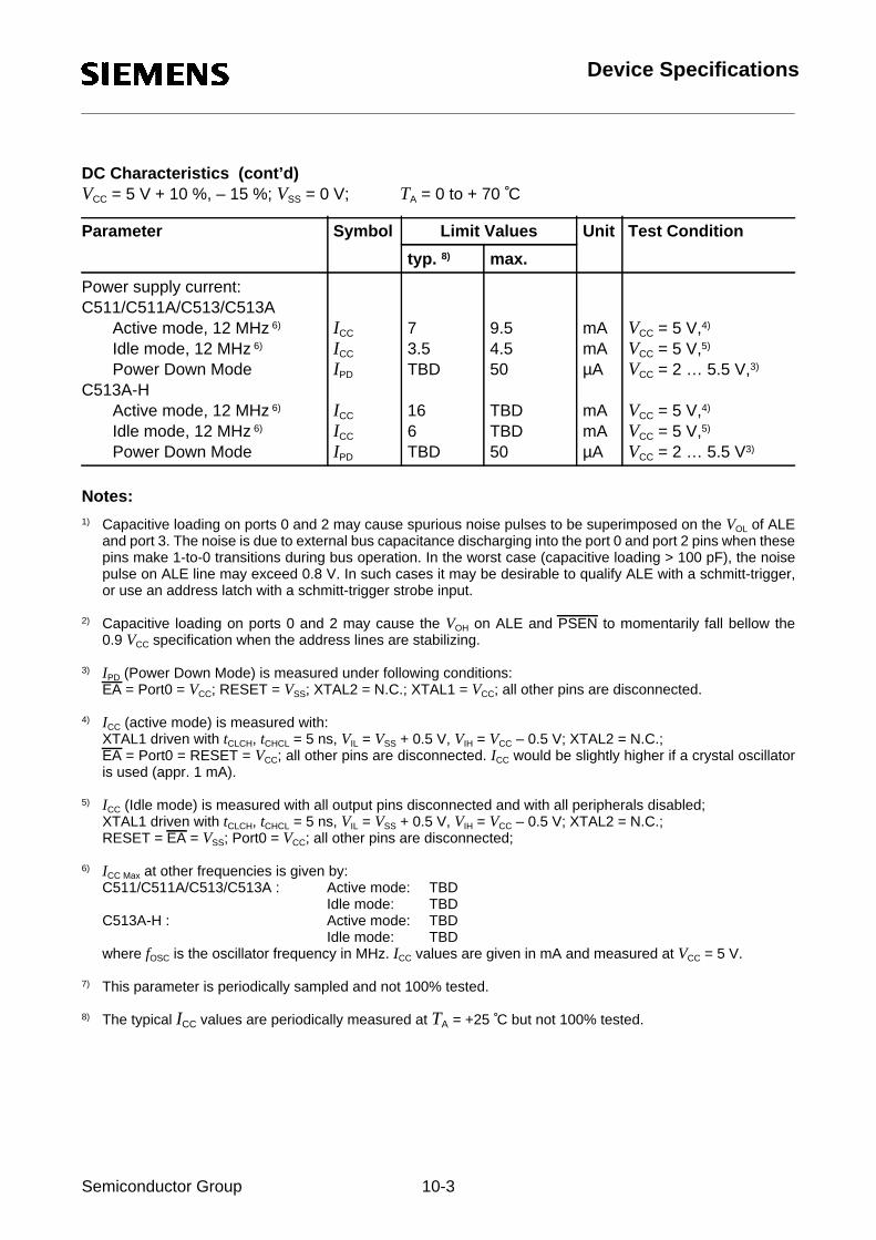
Device Specifications
Notes:1) Capacitive loading on ports 0 and 2 may cause spurious noise pulses to be superimposed on the VOL of ALE
and port 3. The noise is due to external bus capacitance discharging into the port 0 and port 2 pins when thesepins make 1-to-0 transitions during bus operation. In the worst case (capacitive loading > 100 pF), the noisepulse on ALE line may exceed 0.8 V. In such cases it may be desirable to qualify ALE with a schmitt-trigger,or use an address latch with a schmitt-trigger strobe input.
2) Capacitive loading on ports 0 and 2 may cause the VOH on ALE and PSEN to momentarily fall bellow the0.9 VCC specification when the address lines are stabilizing.
3) IPD (Power Down Mode) is measured under following conditions:EA = Port0 = VCC; RESET = VSS; XTAL2 = N.C.; XTAL1 = VCC; all other pins are disconnected.
4) ICC (active mode) is measured with:XTAL1 driven with tCLCH, tCHCL = 5 ns, VIL = VSS + 0.5 V, VIH = VCC – 0.5 V; XTAL2 = N.C.;EA = Port0 = RESET = VCC; all other pins are disconnected. ICC would be slightly higher if a crystal oscillatoris used (appr. 1 mA).
5) ICC (Idle mode) is measured with all output pins disconnected and with all peripherals disabled;XTAL1 driven with tCLCH, tCHCL = 5 ns, VIL = VSS + 0.5 V, VIH = VCC – 0.5 V; XTAL2 = N.C.;RESET = EA = VSS; Port0 = VCC; all other pins are disconnected;
6) ICC Max at other frequencies is given by:C511/C511A/C513/C513A : Active mode: TBD
Idle mode: TBDC513A-H : Active mode: TBD
Idle mode: TBDwhere fOSC is the oscillator frequency in MHz. ICC values are given in mA and measured at VCC = 5 V.
7) This parameter is periodically sampled and not 100% tested.
8) The typical ICC values are periodically measured at TA = +25 ˚C but not 100% tested.
DC Characteristics (cont’d)VCC = 5 V + 10 %, – 15 %; VSS = 0 V; TA = 0 to + 70 ˚C
Parameter Symbol Limit Values Unit Test Condition
typ. 8) max.
Power supply current:C511/C511A/C513/C513A
Active mode, 12 MHz 6)
Idle mode, 12 MHz 6)
Power Down ModeC513A-H
Active mode, 12 MHz 6)
Idle mode, 12 MHz 6)
Power Down Mode
ICC
ICC
IPD
ICC
ICC
IPD
73.5TBD
166TBD
9.54.550
TBDTBD50
mAmAµA
mAmAµA
VCC = 5 V,4)
VCC = 5 V,5)
VCC = 2 … 5.5 V,3)
VCC = 5 V,4)
VCC = 5 V,5)
VCC = 2 … 5.5 V3)
Semiconductor Group 10-3

Device Specifications
10.3 AC Characteristics (applies to all C511/513 Family Microcontrollers)
VCC = 5 V + 10 %, – 15 %; VSS = 0 V TA = 0 C to + 70 C
(CL for port 0, ALE and PSEN outputs = 100 pF; CL for all other outputs = 80 pF)
10.3.1 Program Memory Characteristics
*) Interfacing the C511/513 microcontrollers to devices with float times up to 75 ns is permissible. This limitedbus contention will not cause any damage to port 0 drivers.
Parameter Symbol Limit Values Unit
12 MHzClock
Variable Clock1/tCLCL = 3.5 MHz to 12 MHz
min. max. min. max.
ALE pulse width tLHLL 127 – 2tCLCL – 40 – ns
Address setup to ALE tAVLL 43 – tCLCL – 40 – ns
Address hold after ALE tLLAX 60 – tCLCL – 23 – ns
ALE low to valid instr in tLLIV – 233 – 4tCLCL – 100 ns
ALE to PSEN tLLPL 58 – tCLCL – 25 – ns
PSEN pulse width tPLPH 215 – 3tCLCL – 35 – ns
PSEN to valid instr in tPLIV – 150 – 3tCLCL – 100 ns
Input instruction hold after PSEN tPXIX 0 – 0 – ns
Input instruction float after PSEN tPXIZ*) – 63 – tCLCL – 20 ns
Address valid after PSEN tPXAV*) 75 – tCLCL – 8 – ns
Address to valid instr in tAVIV – 302 – 5tCLCL – 115 ns
Address float to PSEN tAZPL 0 – 0 – ns
Semiconductor Group 10-4

Device Specifications
10.3.2 External Data Memory Characteristics
Parameter Symbol Limit Values Unit
12 MHzClock
Variable Clock1/tCLCL = 3.5 MHz to 12 MHz
min. max. min. max.
RD pulse width tRLRH 400 – 6tCLCL – 100 – ns
WR pulse width tWLWH 400 – 6tCLCL – 100 – ns
Address hold after ALE tLLAX2 132 – 2tCLCL – 35 – ns
RD to valid data in tRLDV – 252 – 5tCLCL – 165 ns
Data hold after RD tRHDX 0 – 0 – ns
Data float after RD tRHDZ – 97 – 2tCLCL – 70 ns
ALE to valid data in tLLDV – 517 – 8tCLCL – 150 ns
Address to valid data in tAVDV – 585 – 9tCLCL – 165 ns
ALE to WR or RD tLLWL 200 300 3tCLCL – 50 3tCLCL + 50 ns
Address valid to WR or RD tAVWL 203 – 4tCLCL – 130 – ns
WR or RD high to ALE high tWHLH 43 123 tCLCL – 40 tCLCL + 40 ns
Data valid to WR transition tQVWX 33 – tCLCL – 50 – ns
Data setup before WR tQVWH 433 – 7tCLCL – 150 – ns
Data hold after WR tWHQX 33 – tCLCL – 50 – ns
Address float after RD tRLAZ – 0 – 0 ns
Semiconductor Group 10-5

Device Specifications
10.3.3 SSC Interface Characteristics
10.3.4 External Clock Characteristics
Parameter Symbol Limit Values Unit
12 MHz Clock
min. max.
Clock Cycle Time : Master ModeSlave Mode
tSCLK
tSCLK
666600
––
nsns
Clock high time tSCH 250 – ns
Clock low time tSCL 250 – ns
Data output delay tD – 100 ns
Data output hold tHO 0 – ns
Data input setup tS 100 – ns
Data input hold tHI 100 – ns
TC bit set delay tDTC – 16 tCLCL ns
Parameter Symbol Limit Values Unit
Variable ClockFreq. = 3.5 MHz to 12 MHz
min. max.
Oscillator period tCLCL 83.3 285 ns
High time tCHCX 20 tCLCL – tCLCX ns
Low time tCLCX 20 tCLCL – tCHCX ns
Rise time tCLCH – 20 ns
Fall time tCHCL – 20 ns
Semiconductor Group 10-6

Device Specifications
Figure 10-1Program Memory Read Cycle
Figure 10-2Data Memory Read Cycle
MCT00096
ALE
PSEN
Port 2
LHLLt
A8 - A15 A8 - A15
A0 - A7 Instr.IN A0 - A7Port 0
t AVLL PLPHtt LLPL
t LLIV
t PLIV
t AZPL
t LLAX t PXIZ
t PXIX
t AVIV
t PXAV
MCT00097
ALE
PSEN
Port 2
WHLHt
Port 0
RD
t LLDV
t RLRHt LLWL
t RLDV
t AVLLt LLAX2
t RLAZ
t AVWL
t AVDV
t RHDX
t RHDZ
A0 - A7 fromRi or DPL from PCL
A0 - A7 Instr.INData IN
A8 - A15 from PCHP2.0 - P2.7 or A8 - A15 from DPH
Semiconductor Group 10-7

Device Specifications
Figure 10-3Data Memory Write Cycle
MCT00098
ALE
PSEN
Port 2
WHLHt
Port 0
WR
t WLWHt LLWL
tQVWX
t AVLLt LLAX2
tQVWH
t AVWL
tWHQX
A0 - A7 fromRi or DPL from PCL
A0 - A7 Instr.INData OUT
A8 - A15 from PCHP2.0 - P2.7 or A8 - A15 from DPH
Semiconductor Group 10-8

Device Specifications
Figure 10-4SSC Timing
Figure 10-5External Clock Drive at XTAL1
Notes: Shown is the data/clock relationship for CPOL = CPHA = 1. The timing diagram isvalid for the other cases accordingly.
In the case of slave mode and CPHA = 0, the output delay for the MSB applies to thefalling edge of SLS (if transmitter is enabled).
In the case of master mode and CPHA = 0, the MSB becomes valid after the data hasbeen written into the shift register, i.e. at least one half SCLK clock cycle before thefirst clock transition.
MCT00033t CHCXt CLCX
CHCLtCLCHt
VCC
t CLCL
- 0.5V
0.45V
CC0.7 V
V - 0.1CC0.2
Semiconductor Group 10-9

Device Specifications
10.3.5 ROM Verification Characteristics (only C511/C511A/C513/C513A)
Figure 10-6ROM Verification Timing
Parameter Symbol Limit Values Unit
min. max.
Address to valid data tAVQV – 48tCLCL ns
ENABLE to valid data tELQV – 48tCLCL ns
Data float after ENABLE tEHQZ 0 48tCLCL ns
Oscillator frequency 1/tCLCL 4 6 MHz
Device Type ROM Size Active AddressLines at Port 2
Inactive AddressLines at Port 2
C511 2.5 KB P2.0 - P2.3 = A8 - A11 P2.4 - P2.6 = VSS
C511A 4 KB P2.0 - P2.3 = A8 - A11 P2.4 - P2.6 = VSS
C513 8 KB P2.0 - P2.4 = A8 - A12 P2.5 - P2.6 = VSS
C513A 12/16 KB P2.0 - P2.5 = A8 - A13 P2.6 = VSS
MCT00049
t AVQV
t EHQZt ELQV
Address
Data OUT
P1.0 - P1.7P2.0 - P2.4
Port 0
P2.7
ENABLE
Inputs: P2.5 - P2.6, PSEN =ALE, EA =RESET =P0.0 - P0.7 = D0 - D7Data:
P2.0 - P2.4 = A8 - A12Address: P1.0 - P1.7 = A0 - A7
V IH
SSV
VSS
Semiconductor Group 10-10

Device Specifications
10.4 AC Characteristics of C513A-H Programming Interface
VCC = 5 V + 10 %, – 15 %; VSS = 0 V; TA = +25 C 10 C; 1/tCLCL = 8 MHz
Parameter Symbol Limit Values Unit
min. max.
ALE pulse width tPLL 60 – ns
Address setup to ALE tPAL 20 – ns
Address hold after ALE tPLA 20 – ns
Address to valid data out tPAD – 230 ns
PRD/PWR pulse width tPCC 250 – ns
PRD to valid data out tPRDV – 200 ns
Data hold after PWR tPWDH 0 – ns
Data float after PRD tPDZ – 40 ns
Chip select setup to ALE active tPCS 0 – ns
Chip select hold after PRD/PWR inactive tPCH 0 – ns
ALE to PWR or PRD tPLC 90 – ns
PWR or PRD high to ALE high tPCL 20 – ns
Data setup before PWR rising edge tPWDS 50 – ns
Data hold after PWR rising edge tPWDH 0 – ns
Data float after PCS tPDF – 40 ns
Semiconductor Group 10-11

Device Specifications
Figure 10-7C513A-H Programming Interface Read Cycle
Figure 10-8C513A-H Programming Interface Write Cycle
Semiconductor Group 10-12

Device Specifications
10.4.1 Reset Characteristics (C513A-H only)
Figure 10-9C513A-H Reset Pulse
Parameter Symbol Limit Values Unit
12 MHzClock
Variable Clock1/tCLCL = 3.5 MHz to 12 MHz
min. max. min. max.
RESET pulse width tRLRH 10 – 10 – ms
t RES
RESET
MCT02420
Semiconductor Group 10-13

Device Specifications
Figure 10-10AC Testing: Input, Output Waveforms
Figure 10-11AC Testing: Float Waveforms
Figure 10-12Recommended Oscillator Circuits for Crystal Oscillator
AC Inputs during testing are driven at VCC - 0.5 V for a logic ’1’ and 0.45 V for a logic ’0’.Timing measurements are made at VIHmin for a logic ’1’ and VILmax for a logic ’0’.
For timing purposes a port pin is no longer floating when a 100 mV change from load voltageoccurs and begins to float when a 100 mV change from the loaded VOH/VOL level occurs.IOL/IOH ≥ ± 20 mA
Semiconductor Group 10-14

Device Specifications
10.5 Package Outlines
Dimensions in mm
Plastic Package, P-LCC-44-2 – SMD(Plastic Leaded Chip-Carrier)
Sorts of PackingPackage outlines for tubes, trays etc. are contained in ourData Book “Package Information”
Dimensions in mmSMD = Surface Mounted Device
Semiconductor Group 10-15

Device Specifications
Dimensions in mm
Plastic Package, P-MQFP-44 – SMD(Plastic Metric Quad Flat Package)
Sorts of PackingPackage outlines for tubes, trays etc. are contained in ourData Book “Package Information”
Dimensions in mmSMD = Surface Mounted Device
Semiconductor Group 10-16