c5545 boosterpack schematic - texas instruments translated to 3.3v and connected to clr# pin of u27...
TRANSCRIPT

5
5
4
4
3
3
2
2
1
1
D D
C C
B B
A A
PAGE CONTENTS
POWER FLOW DIAGRAM
TABLE OF CONTENTS01
REVISION HISTORY02
03
04
REV C
VER 1.4
C5545 BoosterPack
TABLE OF CONTENTS
BLOCK DIAGRAM
POWER ANALYSIS
I2C TREE
06
05
POWER UP SEQUENCE
07
08 C5545 PART A
C5545 POWER09
10
11
OLED , uSD CARD & SPI FLASH
AUDIO CODEC
CC2650 MCU
FT223213
14
POWER15
LAUCHPAD HEADERS12
Title
Size Document Number Rev
Date: Sheet of
Project : Designed for TI by Mistral Solutions Pvt Ltd
BOOST5545ULPMS_TI_C5545BP_SCH_REVC_PRODUCTION C
TABLE OF CONTENTS
C
Friday, September 16, 2016 151
Title
Size Document Number Rev
Date: Sheet of
Project : Designed for TI by Mistral Solutions Pvt Ltd
BOOST5545ULPMS_TI_C5545BP_SCH_REVC_PRODUCTION C
TABLE OF CONTENTS
C
Friday, September 16, 2016 151
Title
Size Document Number Rev
Date: Sheet of
Project : Designed for TI by Mistral Solutions Pvt Ltd
BOOST5545ULPMS_TI_C5545BP_SCH_REVC_PRODUCTION C
TABLE OF CONTENTS
C
Friday, September 16, 2016 151

5
5
4
4
3
3
2
2
1
1
D D
C C
B B
A A
INITIAL DRAFT Mistral Design Team
AUTHORDATEVER # DESCRIPTION OF CHANGES
0.1
REVISION HISTORY
27th APR 2016
0.2 3rd MAY 2016
APPROVED BY
AJIT MB
U19 changed to 4 bit Level translator, RESET_ANDlevel translated to 3.3V and connected to CLR# pin of U27 Mistral Design Team AJIT MB
Mistral Design Team AJIT MBREVIEWED & BASELINED 6th MAY 20161.0
Boosterpack Pin Map Diagram added & Launchpad Header section moved to new sheet
Mistral Design Team AJIT MB1.1 25th AUG 2016
REVIEWED & BASELINED Mistral Design Team AJIT MB1.2 25th AUG 2016
1.4REVIEWED & BASELINED Mistral Design Team AJIT MB
1.3 16th SEP 2016 BoosterPack Pin Map Color code updated as per the customer review comments
Mistral Design Team AJIT MB
16th SEP 2016
Title
Size Document Number Rev
Date: Sheet of
Project : Designed for TI by Mistral Solutions Pvt Ltd
BOOST5545ULPMS_TI_C5545BP_SCH_REVC_PRODUCTION C
REVISION HISTORY
C
Friday, September 16, 2016 152
Title
Size Document Number Rev
Date: Sheet of
Project : Designed for TI by Mistral Solutions Pvt Ltd
BOOST5545ULPMS_TI_C5545BP_SCH_REVC_PRODUCTION C
REVISION HISTORY
C
Friday, September 16, 2016 152
Title
Size Document Number Rev
Date: Sheet of
Project : Designed for TI by Mistral Solutions Pvt Ltd
BOOST5545ULPMS_TI_C5545BP_SCH_REVC_PRODUCTION C
REVISION HISTORY
C
Friday, September 16, 2016 152
5
5
4
4
3
3
2
2
1
1
D D
C C
B B
A A
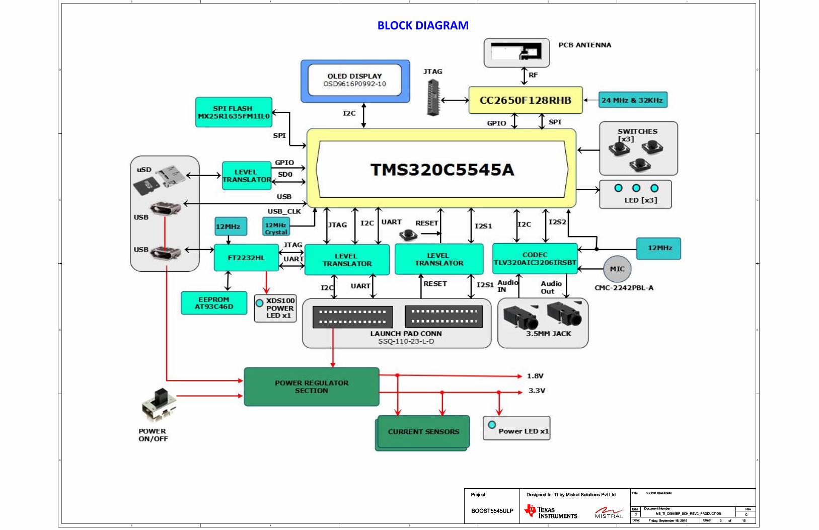
BLOCK DIAGRAM
Title
Size Document Number Rev
Date: Sheet of
Project : Designed for TI by Mistral Solutions Pvt Ltd
BOOST5545ULPMS_TI_C5545BP_SCH_REVC_PRODUCTION C
BLOCK DIAGRAM
C
Friday, September 16, 2016 153
Title
Size Document Number Rev
Date: Sheet of
Project : Designed for TI by Mistral Solutions Pvt Ltd
BOOST5545ULPMS_TI_C5545BP_SCH_REVC_PRODUCTION C
BLOCK DIAGRAM
C
Friday, September 16, 2016 153
Title
Size Document Number Rev
Date: Sheet of
Project : Designed for TI by Mistral Solutions Pvt Ltd
BOOST5545ULPMS_TI_C5545BP_SCH_REVC_PRODUCTION C
BLOCK DIAGRAM
C
Friday, September 16, 2016 153

5
5
4
4
3
3
2
2
1
1
D D
C C
B B
A A
POWER DISTRIBUTION DIAGRAM
Title
Size Document Number Rev
Date: Sheet of
Project : Designed for TI by Mistral Solutions Pvt Ltd
BOOST5545ULPMS_TI_C5545BP_SCH_REVC_PRODUCTION C
POWER DISTRIBUTION DIAGRAM
C
Friday, September 16, 2016 154
Title
Size Document Number Rev
Date: Sheet of
Project : Designed for TI by Mistral Solutions Pvt Ltd
BOOST5545ULPMS_TI_C5545BP_SCH_REVC_PRODUCTION C
POWER DISTRIBUTION DIAGRAM
C
Friday, September 16, 2016 154
Title
Size Document Number Rev
Date: Sheet of
Project : Designed for TI by Mistral Solutions Pvt Ltd
BOOST5545ULPMS_TI_C5545BP_SCH_REVC_PRODUCTION C
POWER DISTRIBUTION DIAGRAM
C
Friday, September 16, 2016 154

5
5
4
4
3
3
2
2
1
1
D D
C C
B B
A A
POWER ANALYSIS
Title
Size Document Number Rev
Date: Sheet of
Project : Designed for TI by Mistral Solutions Pvt Ltd
BOOST5545ULPMS_TI_C5545BP_SCH_REVC_PRODUCTION C
POWER ANALYSIS
C
Friday, September 16, 2016 155
Title
Size Document Number Rev
Date: Sheet of
Project : Designed for TI by Mistral Solutions Pvt Ltd
BOOST5545ULPMS_TI_C5545BP_SCH_REVC_PRODUCTION C
POWER ANALYSIS
C
Friday, September 16, 2016 155
Title
Size Document Number Rev
Date: Sheet of
Project : Designed for TI by Mistral Solutions Pvt Ltd
BOOST5545ULPMS_TI_C5545BP_SCH_REVC_PRODUCTION C
POWER ANALYSIS
C
Friday, September 16, 2016 155

5
5
4
4
3
3
2
2
1
1
D D
C C
B B
A A
POWER UP SEQUENCE
Note:-180ms delay added for OLED Reset to meet the specifications
USB POWER SEQUENCE
Title
Size Document Number Rev
Date: Sheet of
Project : Designed for TI by Mistral Solutions Pvt Ltd
BOOST5545ULPMS_TI_C5545BP_SCH_REVC_PRODUCTION C
POWER UP SEQUENCE
C
Friday, September 16, 2016 156
Title
Size Document Number Rev
Date: Sheet of
Project : Designed for TI by Mistral Solutions Pvt Ltd
BOOST5545ULPMS_TI_C5545BP_SCH_REVC_PRODUCTION C
POWER UP SEQUENCE
C
Friday, September 16, 2016 156
Title
Size Document Number Rev
Date: Sheet of
Project : Designed for TI by Mistral Solutions Pvt Ltd
BOOST5545ULPMS_TI_C5545BP_SCH_REVC_PRODUCTION C
POWER UP SEQUENCE
C
Friday, September 16, 2016 156

5
5
4
4
3
3
2
2
1
1
D D
C C
B B
A A
I2C TREE
Audio Codec 0x18
I2C DEVICES 7 BIT ADDRESS
OLED Display
0x40 ,0x41, 0x44, 0x48INA Devices
I2C ADDRESS TABLE
0x3C
Title
Size Document Number Rev
Date: Sheet of
Project : Designed for TI by Mistral Solutions Pvt Ltd
BOOST5545ULPMS_TI_C5545BP_SCH_REVC_PRODUCTION C
I2C TREE
C
Friday, September 16, 2016 157
Title
Size Document Number Rev
Date: Sheet of
Project : Designed for TI by Mistral Solutions Pvt Ltd
BOOST5545ULPMS_TI_C5545BP_SCH_REVC_PRODUCTION C
I2C TREE
C
Friday, September 16, 2016 157
Title
Size Document Number Rev
Date: Sheet of
Project : Designed for TI by Mistral Solutions Pvt Ltd
BOOST5545ULPMS_TI_C5545BP_SCH_REVC_PRODUCTION C
I2C TREE
C
Friday, September 16, 2016 157

5
5
4
4
3
3
2
2
1
1
D D
C C
B B
A A
RESET CIRCUIT
Micro USB Device
C5545 PART A
RTC POWERDSP CLOCK SELECTION
USB POWER LOAD SWITCH
Jumper
Internal
External ClockNo Jumper
Jumper
CLOCK Selection
RESET#_AND
PWRST
DSP_USB_DMDSP_USB_DP
LDO_EN
BG_CAP
CONN_USB_VBUS
DSP_RTC_XO
DSP_RTC_XIDSP_RTC_XO
DSP_RTC_XI
CVDDRTC
USB_MXI
DSP_USB_DPDSP_USB_DM
DSP_USB_VBUS
USB_R1USB_VSSREF
USB_VDDOSCUSB_VDDOSC
USB_VDDOSCINT0#INT1#
DSP_EMU1DSP_EMU0
CLKOUTDSP_CLKSEL
DSP_I2C_SCLDSP_I2C_SDA
DSP_SPI_CS3
DSP_SPI_CS3
CVDDRTC
CVDDRTC
DSP_CLKSEL
DSP_USB_VBUSCONN_USB_VBUS
GPAIN3GPAIN2GPAIN1
DSP_SD0_CMD
USB_MXI
USB_MXO
USB_MXO
DGND
VCC1V8VCC1V8
DGND
DGND
DGNDDGND
DGND GNDUSB1
DGND
DGND GNDUSB1
DGND
DC_5V_IN
VCC1V8
DGND
DGND
VCC1V8VCC1V8
AGND
VCC1V8
DGND
DGNDDGND
VCC3V3_USB
DGND
VCC1V8VCC1V3
VCC1V8
DGND
DGNDDGND
DGND DGND
VCC3V3_USB_LDSWVCC3V3VCC3V3_USB
DGND
DGND
AGND
VCC1V3_USB_EN
VCC1V8
DGND
DGND
DGND
VCC1V8
VSSRTC
VSSRTC
USB_VSSOSC
USB_VSSOSC
USB_VSSOSC
LP_RSTOUT 12
DSP_I2C_SCL 9,10,14
DSP_I2C_SDA 9,10,14
DSP_SPI_TX 11,14DSP_SPI_RX 11,14
DSP_SPI_CS2 11DSP_SPI_CS0 14
DSP_UART_TX 9DSP_SPI_CLK 11,14
DSP_UART_RX 9DSP_SDCD 14
LED3 10
DSP_I2S2_CLK 10DSP_I2S2_FS 10
DSP_I2S2_RX 10DSP_I2S2_DX 10
SWITCH2 10SWITCH3 10SWITCH4 10
LED1 10LED2 10
DSP_TRSTN13DSP_TCK13DSP_TMS13
DSP_TDI13
DSP_12MHz10
DSP_SD0_DAT014DSP_SD0_DAT114DSP_SD0_DAT214DSP_SD0_DAT314DSP_SD0_CMD14DSP_SD0_CLK14
DSP_I2S1_CLK12
DSP_I2S1_FS12
DSP_I2S1_RX12
DSP_I2S1_DX12
CC2650_PWRMGT111CC2650_PWRMGT211
LP_BUFF_SOFT_RST 121V3_PWRGD 15
VCC_SEL_LDOI9
DSP_TDO13
CC2650_RESET# 11
RESET#_AND10,11,13,14
FT2232_RTS_RESET 13
Title
Size Document Number Rev
Date: Sheet of
Project : Designed for TI by Mistral Solutions Pvt Ltd
BOOST5545ULPMS_TI_C5545BP_SCH_REVC_PRODUCTION C
C5545 PART A
C
Friday, September 16, 2016 158
Title
Size Document Number Rev
Date: Sheet of
Project : Designed for TI by Mistral Solutions Pvt Ltd
BOOST5545ULPMS_TI_C5545BP_SCH_REVC_PRODUCTION C
C5545 PART A
C
Friday, September 16, 2016 158
Title
Size Document Number Rev
Date: Sheet of
Project : Designed for TI by Mistral Solutions Pvt Ltd
BOOST5545ULPMS_TI_C5545BP_SCH_REVC_PRODUCTION C
C5545 PART A
C
Friday, September 16, 2016 158
R14 0E_1%
R118 0E_1%
R94 10K_1%
R142
6.2K_1%
DNI
C145
1uF
FL5
600E
1 2
D11SS416
2 1
C47
0.1uF
R123 0EDNI
C310.1uF
R20
4.7K
D9
TPD1E10B06DPY
21
C10.01uF
R124 0E
C51
10uF
R147 0E_1%DNI
R21
4.7K
R18
10K_1%
R134
10K_1%
R11 0E_1%
U25
TPS22913BYZVT
VOUTA1
VINA2
GND
B1
ONB2
C60
0.1uF
R1484.7K
R4100K
C30.1uF
R135
10K_1%
R5100K
R23
10K_1%
R17 10K_1%DNI
U24
TPS22913BYZVT
VOUTA1
VINA2
GND
B1
ONB2
C8 22pF
C156
22pF
U143
SN74LVC1G08
1
24
35
U1A
TMS320C5545AZQW 10
INT0B12
INT1C11
TDIB4
TDOD1
SCLB11
SDAD11
CLKINE12
CLKOUTC12
CLK_SELD12
RTC_XIF11
RTC_XOE11
RESETA11
TMSD3
TCKC1
TRSTF2
USB_MXIL9
USB_MXOK9
SD0_D0/I2S0_DX/GP[2]D5
SD0_D1/I2S0_RX/GP[3]G2
SD0_D2/GP[4]M3
SD0_D3/GP[5]G3
SD0_CMD/I2S0_FS/GP[1]J2
SD0_CLK/I2S0_CLK/GP[0]E5
SD1_D0/I2S1_DX/GP[8]L3
SD1_D1/I2S1_RX/GP[9]H3
SD1_D2/GP[10]M4
SD1_D3/GP[11]G5
SD1_CMD/I2S1_FS/GP[7]L4
SD1_CLK/I2S1_CLK/GP[6]H5
CVDDRTCD10
BG_CAPJ11
DSP_LDO_ENM12
USB_VBUSK5
USB_DPL6
USB_R1K7USB_DMM6
LCD_D[2]/GP[12]E2
LCD_D[3]/GP[13]E1
LCD_D[4]/GP[14]F1
LCD_D[5]/GP[15]G1
LCD_D[6]/GP[16]E3
LCD_D[7]/GP[17]J1
LCD_D[8]/I2S2_CLK/GP[18]/SPI_CLKH1
LCD_D[9]/I2S2_FS/GP[19]/SPI_CS0K1
LCD_D[10]/I2S2_RX/GP[20]/SPI_RXF5
LCD_D[11]/I2S2_DX/GP[27]/SPI_TXK2
LCD_D[12]/UART_RTS/GP[28]/I2S3_CLKJ3
LCD_D[13]/UART_CTS/GP[29]/I2S3_FSM1
LCD_D[14]/UART_RXD/GP[30]/I2S3_RXL1
LCD_D[15]/UART_TXD/GP[31]/I2S3_DXL2
LCD_EN_RDB/SPI_CLKA1
LCD_CS0_E0/SPI_CS0A2
LCD_RW_WRB_SPI_CS2B2
LCD_RS/SPI_CS3A3
LCD_D[0]/SPI_RXA4
LCD_D[1]/SPI_TXC2
GPAIN1F8
GPAIN2F10
GPAIN3J12
RSV0L12
RSV4H10
RSV5J10
RSV3K11
RSV17M5
EMU0B3
EMU1B1
USB_VSSREFH8
USB_VSSOSCM9
USB_VDDOSCK8
VSSRTCG12
DVDDRTCF12
D2
RB578VAM100TR
21
Y612.000MHz
1
42
3
R74.7K
C7 22pF
R117
10K_1%
R13 0E_1%
R84.7K
R10 0E_1%
R136
10K_1%
Y1
32.768 Khz
12
J1
CON_MUSB-B_5_F
VBUS1
D+3 D-2
ID4
SH1
6
GND5
SH49
SH38
SH2
7SH6
11
SH5
10
C157
22pF
J2
HDR_1X2
12
TP1SMD
R15 0E_1%
C4
0.1uF
R1100K
R371K
D-
D+
D8
TPD2EUSB30DRTR
3
21
R9210K_1%
C23 0.01uF
SW1
PTS820 J20M SMTR LFS
1 23 4
5 6
R16 0E_1%
R98 47E_1%
C48
0.1uF
R2100KC1580.01uF
R2220K_1%
R6710K_1%
C2
0.1uF
R12 0E_1%
R9 8.06K_1%
C5
10uF
C6
0.1uF
U26
SN74LVC1G11DCKR
1
2
34
5
6
FB1
120E
R196.8K_1%
C141
1uF

5
5
4
4
3
3
2
2
1
1
D D
C C
B B
A A
C5545 POWER
I2C LEVEL TRANSLATOR
UART JUMPER SELECTION
Launch Pad & CC2650
B/W Pin 1 & 3 FT2232 & C5545
Jumper Connected Devices
UART JUMPER SELECTION
B/W Pin 2 & 4
B/W Pin 1 & 2FT2232 & CC2650
B/W Pin 3 & 4Launch Pad & C5545
Header
JP2 & JP3
JP2 & JP3
JP2
JP3
JP2
JP3
B/W Pin 3 & 4
B/W Pin 1 & 2
I2C Address : 0x40
I2C Address : 0x48 I2C Address : 0x44
I2C Address : 0x41
USB_VDDA1P3
USB_VDD1P3
USB_VDDA3P3
USB_VDDPLL
I2C_LVL_EN
USB_VDD1P3
ANA_1V3
USB_VDDA3P3
USB_VDDPLLUSB_VDDA1P3
LDOI
3V3_I2C1_SDA
DGND
DGND
DSP_LDOOUSB_LDOO
ANA_LDOO
CVDD
DGND
CVDD
USB_LDOO
DGND
DSP_LDOO
DGND
ANA_1V3
DGNDDGND
DGND
DGND
DGND
VCC1V8 VCC3V3
VCC3V3
VCC3V3
DGND
DGND
CVDD
VCC3V3
DGND
DGND
DSP_DVDDIO
DSP_DVDDIO VCC1V8
DSP_DVDDIO
AGNDAGND
AGND
AGND
AGND
DGNDAGND
AGND
VCC1V3
DSP_LDOO
VCC1V3
USB_LDOO
ANA_LDOO
VCC1V3
VCC3V3_USB
VCC1V3_USB_EN
VCC1V8 VCC1V8
VCC1V8 VCC1V8
VCC3V3
DGND
DGND
VCC3V3_USB VCC3V3_USB_LDSW
VCC3V3
DGND
DGND
VCC1V8
VCC3V3
DGNDDGND
VCC3V3
DSP_I2C_SCL8,10,14
DSP_I2C_SDA8,10,14 3V3_I2C1_SDA 9,12
3V3_I2C1_SCL 9,12
FT2232_BUFF_UART_TX13
DSP_UART_RX8 LP_BUFF_UART_TX 12
LP_BUFF_UART_RX 12DSP_UART_TX8
FT2232_BUFF_UART_RX13
3V3_I2C1_SDA9,123V3_I2C1_SCL9,12 3V3_I2C1_SDA9,12
3V3_I2C1_SCL9,12
CC2650_UART_TX 11
CC2650_UART_RX 11
3V3_I2C1_SDA9,123V3_I2C1_SCL9,12
3V3_I2C1_SCL 9,123V3_I2C1_SDA 9,12
VCC_SEL_LDOI8
Title
Size Document Number Rev
Date: Sheet of
Project : Designed for TI by Mistral Solutions Pvt Ltd
BOOST5545ULPMS_TI_C5545BP_SCH_REVC_PRODUCTION C
C5545 POWER
C
Friday, September 16, 2016 159
Title
Size Document Number Rev
Date: Sheet of
Project : Designed for TI by Mistral Solutions Pvt Ltd
BOOST5545ULPMS_TI_C5545BP_SCH_REVC_PRODUCTION C
C5545 POWER
C
Friday, September 16, 2016 159
Title
Size Document Number Rev
Date: Sheet of
Project : Designed for TI by Mistral Solutions Pvt Ltd
BOOST5545ULPMS_TI_C5545BP_SCH_REVC_PRODUCTION C
C5545 POWER
C
Friday, September 16, 2016 159
C17
0.1uF
C52
0.1uFC18
0.1uF
C10
0.01uF
JP3
HDR_2X2
1 23 4
C37
0.1uF
C35
1uF
R27
4.7K
C32
1uF
C9
1uF
R133 0E
C540.01uF
C26
0.01uF
C25
1uF
C20
10uF
C38
0.1uF
C22
10uF
FL6
600E
1 2
C12
0.01uF
R139
1E_1%
C28
0.01uF
FL4
600E
1 2
U30
INA219AIDCNR
VIN+
1
VIN-
2
GND3
VS4
SCL
5
SDA
6
A0
7
A1
8
C44
1uF
C49
0.1uF
C13
0.01uF
FL3
600E
1 2
FL1
600E
1 2
C29
0.01uF
C41
10uF
C45
0.1uF
C33
0.01uF
U4
INA219AIDCNR
VIN+
1VIN-
2
GND3
VS4
SCL
5SDA
6
A0
7A1
8
C46
0.1uF
U23
INA219AIDCNR
VIN+
1VIN-
2
GND3
VS4
SCL
5SDA
6
A0
7A1
8
FL2
600E
1 2
C530.01uF
C14
0.01uF
R128 0E
DNI
R137
1E_1%R1300E
DNI
C24
0.1uFC148
0.1uF
U5
INA219AIDCNR
VIN+
1VIN-
2
GND3
VS4
SCL
5SDA
6
A0
7A1
8
R129 0ER25
1E_1%
R24
1E_1%
C15
0.01uF
R38100K
R1310ER29 0E
R121100K
R36100K
C42
0.1uF
C36
0.1uF
U1B
TMS320C5545AZQW 10
CVDDA9
CVDDB5
CVDDB8
CVDDC6
CVDDE6
CVDDG7
CVDDJ9
DVDDIOB10
DVDDIOD2
DVDDIOH2
DVDDIOM2
VDDA_PLLE10
VDDA_ANAG11
USB_VDDPLLM7
USB_VDDA1P3K6
USB_VDDA3P3L7
USB_VDD1P3L5
USB_VDD1P3M8
LDOIG10
LDOIL10
LDOIL11
DSP_LDOOM11
USB_LDOOM10
ANA_LDOOH11
VSSA5
VSSA6
VSSA7
VSSA8
VSSA10
VSSA12
VSSB6
VSSB7
VSSB9
VSSC4
VSSC7
VSSC9
VSSF3
VSSF7
VSSG6
VSSG8
VSSK4
VSSA_PLLE8
VSSA_ANAH12
VSSA_ANAK12
USB_VSSA3P3H7
USB_VSS1P3H6
USB_VSSPLLL8
C16
0.01uF
R59100K
C43
0.1uF
C34
0.01uF
R132 0E
DNI
C11
0.01uF
JP2
HDR_2X2
1 23 4
C39
1uF
C30
0.1uF
R28
10K_1%
R350E
DNI
U6
TCA9517DGKR
VCCA
1
SCLA2
SDAA3
GND
4
EN5
SDAB6
SCLB7
VCCB
8
R26
4.7K
C27
0.01uF

5
5
4
4
3
3
2
2
1
1
D D
C C
B B
A A
AUDIO CODEC
Head phone
Stereo Line IN
Mic
SWITCHES & LEDs
GREEN GREENGREEN
I2C Address : 0x18
12MHz_AUD_MCLK
FLY_NFLY_P
VNEG
REF
IN3_RHP_MIC GPIO_AUD
IN1_LIN1_R
AVDD_1V8
MICBIAS_RMICBIAS
IN1_L
IN1_R
HPLHPR
GND_SENSE
GND_SENSE
MICBIAS
MIC
MIC
SWITCH2
12MHz_AUD_MCLKSTDBY_OSC1V8
SWITCH4SWITCH3
MICBIAS_R
MICBIAS_R
HPR
HPL
HP_MICMICBIAS
GND_SENSE
DGND DGND AUD_AGNDAUD_AGND
AUD_AGND DGND
VCC1V8
DGNDDGNDAUD_AGND
AUD_AGND
AUD_AGNDAUD_AGND
DGND DGND DGND
VCC1V8 VCC1V8 VCC1V8
DGND
VCC1V8
DGND
VCC1V8VCC1V8
VCC1V8
VCC3V3 VCC3V3 VCC3V3
AUD_AGND
DGND
AUD_AGND
DSP_I2S2_RX 8DSP_I2S2_DX 8
DSP_I2S2_CLK8DSP_I2S2_FS8
DSP_I2C_SDA8,9,14
RESET#_AND8,11,13,14
DSP_12MHz 8
SWITCH2 8SWITCH3 8SWITCH4 8
LED18 LED28 LED38
DSP_I2C_SCL8,9,14
Title
Size Document Number Rev
Date: Sheet of
Project : Designed for TI by Mistral Solutions Pvt Ltd
BOOST5545ULPMS_TI_C5545BP_SCH_REVC_PRODUCTION C
AUDIO CODEC , SWITCHES & LEDs
C
Friday, September 16, 2016 1510
Title
Size Document Number Rev
Date: Sheet of
Project : Designed for TI by Mistral Solutions Pvt Ltd
BOOST5545ULPMS_TI_C5545BP_SCH_REVC_PRODUCTION C
AUDIO CODEC , SWITCHES & LEDs
C
Friday, September 16, 2016 1510
Title
Size Document Number Rev
Date: Sheet of
Project : Designed for TI by Mistral Solutions Pvt Ltd
BOOST5545ULPMS_TI_C5545BP_SCH_REVC_PRODUCTION C
AUDIO CODEC , SWITCHES & LEDs
C
Friday, September 16, 2016 1510
U9
TLV320AIC3206IRSBT
DVSS
1
DVSS
2
IOVSS
11
AVSS
21
EP
41
IOVDD
10
AVDD
29
DRVDD_HP
32
DVDD_CP
39
DVDD
40
RESET3
GPIO/MFP54
MCLK5
BCLK6
WCLK7
DIN/MFP18
DOUT/MFP29
SCLK/MFP312
MISO/MFP415
GND_SENSE28
DVSS_CP
37
SPI/SELECT16
IN1_L17
IN1_R18
IN2_L19
IN2_R20
REF22
MICBIAS23
IN3_L24
IN3_R25
VSYS
30
MICDET34
VNEG35
FLY_N36
FLY_P38
SDA/MOSI14 SCL/SSZ13
LOL26
LOR27
HPL31
HPR33
R5810K_1%
R138 2.7K
C76
0.1uF
C74
0.1uF
R47
10K_1%
C79 2.2uF
Q3
BSS138
3
1
2
R41 0E_1%
SW4
PTS820 J20M SMTR LFS
1 23 4
5 6
FB4
220E
12
R491K
C82
2.2uF
C96
0.1uF
R44 2.7K
R43 0E_1%
R5610K_1%
FB5
120E
LD1
SML-P11MTT86
2 1
Q2
BSS138
3
1
2
R501K
FB8
120E
SW2
PTS820 J20M SMTR LFS
1 23 4
5 6
LD2
SML-P11MTT86
2 1
R511K
C1500.1uF
LD3
SML-P11MTT86
2 1
R48 0E_1%
C75
10uF
R5410K_1%
MK1
CMC-2242PBL-A
12
Q1
BSS138
3
1
2 R5710K_1%
J6
CON_AUDIOJACK4_SJ-43514
4
3
2
1
R39 2.7K
C143 0.47uF
R5310K_1%
C132
0.1uF
C71 0.1uF
C73 0.1uF
C144 0.47uF
C69
10uF
C70
0.1uF
C830.1uF
R42 0E_1%
R46 0E_1%
SW3
PTS820 J20M SMTR LFS
1 23 4
5 6
C800.01uF
TP2SMD
C78
0.1uF
U10
12.00MHz
STANDBY1
GND
2
OUTPUT3V
DD
4
R5210K_1%
C81 10uF
J5
CON_AUDIOJACK4_SJ-43514
4
3
2
1
R451K
R40 0E_1%
C149 0.1uF

5
5
4
4
3
3
2
2
1
1
D D
C C
B B
A A
R91 and C140 forantenna matching
CC2650 MCU
JTAG HEADER
2.4GHz
X24M_P
X24M_N
X32K_Q1
X32K_Q2
CC2650_TDOCC2650_TDI
DCOUPL
X24M_NX24M_P
X32K_Q1X32K_Q2
CC2650_TMSCC2650_TCK
RF_PRF_N
RF_P
RF_N
CC2650_SPI_TX
CC2650_SPI_CS
CC2650_SPI_RXCC2650_SPI_SCK
CC2650_TMSCC2650_TCK
CC2650_TDICC2650_TDO
RESET_JTAG
RESET_NRESET_JTAG
DGND DGND
DGND
VCC1V8
DGND
VCC1V8_CC2650
DGND
VCC1V8_CC2650
DGND DGND
DGND DGND DGND
DGND
VCC1V8
DGND
VCC1V8
DGND
VCC1V8
CC2650_PWRMGT1 8CC2650_PWRMGT2 8
CC2650_UART_RX 9
CC2650_UART_TX 9
DSP_SPI_CS2 8DSP_SPI_CLK 8,14DSP_SPI_TX 8,14DSP_SPI_RX 8,14
RESET#_AND8,10,13,14CC2650_RESET#8
Title
Size Document Number Rev
Date: Sheet of
Project : Designed for TI by Mistral Solutions Pvt Ltd
BOOST5545ULPMS_TI_C5545BP_SCH_REVC_PRODUCTION C
CC2650 MCU
C
Friday, September 16, 2016 1511
Title
Size Document Number Rev
Date: Sheet of
Project : Designed for TI by Mistral Solutions Pvt Ltd
BOOST5545ULPMS_TI_C5545BP_SCH_REVC_PRODUCTION C
CC2650 MCU
C
Friday, September 16, 2016 1511
Title
Size Document Number Rev
Date: Sheet of
Project : Designed for TI by Mistral Solutions Pvt Ltd
BOOST5545ULPMS_TI_C5545BP_SCH_REVC_PRODUCTION C
CC2650 MCU
C
Friday, September 16, 2016 1511
C85
0.1uF
C140
DNI
J12
HDR_2X5
246810
13579
R91 0E
C840.01uF
R14110K_1%
Y2
24.0000MHz
1
4 2
3
C87
0.1uF
C1371.2pF
Y3
32.768KHz
12
C95
1uF
C88
10uF
L315nH
R85 100E
C1461.2pF
C89
0.1uF
R65
10K_1%
C93 15pF
U11
CC2650F128RHBT
EP
33
DIO_06
DIO_17
DIO_28
DIO_39
DIO_410
DIO_515
DIO_616
DIO_720
DIO_821
DIO_922
DIO_1023
DIO_1124
DIO_1225
DIO_1326
DIO_1427
VDDS2
11
DCOUPL12
DCDC_SW
17
VDDS_DCDC
18
VDDS
28
VDDR
29
VDDR_RF
32
RF_P1
RF_N2
RX_TX3
X32K_Q14
X32K_Q25
JTAG_TMSC13
JTAG_TCKC14
RESET_N19
X24M_N30
X24M_P31
C94 15pF
U31
SN74LVC1G11DCKR
1
2
3 4
5
6
C139 12pFL4
2nH
C86
0.1uF
FL7
1.5KE
1 2

5
5
4
4
3
3
2
2
1
1
D D
C C
B B
A A
LAUNCH PAD HEADERS
SIGNAL DIRECTION SIGNAL DIRECTION
1A ------> 1B
2A <------ 2B
1A <------ 1B
2A <------ 2B
I2S1_BUFF_1DIR
LP_AUD_DINLP_AUD_DOUTLP_AUD_CLKLP_AUD_SYNC
LP_UART_TXLP_AUD_DOUTLP_UART_RXLP_AUD_DIN
I2S1_BUFF_1DIRI2S1_BUFF_2DIR
LP_3V3
LP_AUD_CLKLP_AUD_SYNC
I2S1_BUFF_2DIR
LP_SOFT_RST
LP_5V
LP_SOFT_RST
LP_GND
LP_UART_RXLP_UART_TX
LP_I2C_SDALP_I2C_SCL
LP_GND
DC_5V_IN
DGNDDGND
DGND DGND
DGND
VCC1V8 VCC3V3_LP
DGND
VCC1V8 VCC3V3_LPVCC1V8
DGNDDGND
VCC3V3_LP
DGND
VCC1V8
VCC3V3_LP
VCC3V3_LP
DGND
VCC1V8
DGND
DGND LP_GND
LP_BUFF_UART_TX 9DSP_I2S1_FS8
DSP_I2S1_CLK8DSP_I2S1_RX 8
3V3_I2C1_SDA93V3_I2C1_SCL9
LP_BUFF_SOFT_RST8
LP_RSTOUT 8
LP_BUFF_UART_RX 9DSP_I2S1_DX 8
Title
Size Document Number Rev
Date: Sheet of
Project : Designed for TI by Mistral Solutions Pvt Ltd
BOOST5545ULPMS_TI_C5545BP_SCH_REVC_PRODUCTION C
LAUNCHPAD HEADERS
C
Friday, September 16, 2016 1512
Title
Size Document Number Rev
Date: Sheet of
Project : Designed for TI by Mistral Solutions Pvt Ltd
BOOST5545ULPMS_TI_C5545BP_SCH_REVC_PRODUCTION C
LAUNCHPAD HEADERS
C
Friday, September 16, 2016 1512
Title
Size Document Number Rev
Date: Sheet of
Project : Designed for TI by Mistral Solutions Pvt Ltd
BOOST5545ULPMS_TI_C5545BP_SCH_REVC_PRODUCTION C
LAUNCHPAD HEADERS
C
Friday, September 16, 2016 1512
R126
10K_1%
DNI
J8
RECP_2X10
135791113151719
2468101214161820
R127
10K_1%
R63 0E_1%
U12
SN74AVC4T245RSVR
VCCA
3
VCCB
2
GND1
10
GND2
11
1DIR4
2DIR5
1A16
1A27
2A18
2A29
1OE1
2OE16
1B115
1B214
2B113
2B212
FB6
120E
R6110K_1%
R6010K_1%
R6410K_1%
R6610K_1%
U13
SN74AVC4T245RSVR
VCCA
3
VCCB
2
GND1
10
GND2
11
1DIR4
2DIR5
1A16
1A27
2A18
2A29
1OE1
2OE16
1B115
1B214
2B113
2B212
D3
RB578VAM100TR
2 1
C99
0.1uF
R140100K
J7
RECP_2X10
135791113151719
2468101214161820
C100
0.1uFC97
0.1uF
C98
0.1uF
R62 0E_1%

5
5
4
4
3
3
2
2
1
1
D D
C C
B B
A A
Micro USB DEBUG
FT2232 JTAG/DEBUG
LEVEL TRANSLATOR
GREEN
SIGNAL DIRECTION SIGNAL DIRECTION
A ------> B 1A <------ 1B2A <------ 2B
TCKTDI
TMSTRSTN
TDO
12MHz_FT2232STDBY_OSC3V3
12MHz_FT2232
FT2232_USB_DPFT2232_USB_DM
FT2232_USB_VBUS
FT2232_REF
FT2232_EECSFT2232_EEDATA
FT2232_EECLK
RTCK FT2232_TCK
FT2232_TRSTN
DIS
SRST_N_OUT
PWR_DETSRST_N_IN
FT2232_RESET
FT2232_RESETPWR_RST
FT2232_EECSFT2232_EECLK
FT2232_DOFT2232_EEDATA
PWR_DET
PWR_RST
FT2232_USB_DPFT2232_USB_DM
PWRSAV#
FT2232_USB_VBUS
PWRSAV#
UNUSED_2B2
UNUSED_2B2
DGND
DGND
VCC3V3
DGND
DGND
DGND
DGNDGNDUSB2
DGND GNDUSB2
DGND
VCC1V8_FT2232
VCC1V8_FT2232
DGND
VPHY_FT2232
VPLL_FT2232
VPHY_FT2232VPLL_FT2232
DGND
DGND
VCC1V8_FT2232
DGND
DGND
DGND DGND
DGNDDGND
VCC1V8
DC_5V_IN
VCC1V8
DGND
DGND
VCC3V3VCC3V3
VCC3V3
VCC3V3
VCC3V3
VCC3V3
VCC3V3
VCC3V3
VCC3V3
DGND
DGND
VCC3V3
DGND
VCC3V3
DGND
VCC3V3
DGND
DGND
VCC3V3
DGND
DGND
DGND
VCC3V3
DGND
DGND
DGND
FT2232_TCK 13
FT2232_TMS 13FT2232_TRSTN 13
FT2232_TCK13
FT2232_TMS13FT2232_TRSTN13
DSP_TCK 8DSP_TDI 8DSP_TMS 8DSP_TRSTN 8
FT2232_UART_RX 13
FT2232_UART_TX 13
FT2232_UART_TX13 FT2232_BUFF_UART_TX 9 FT2232_UART_RX13 FT2232_BUFF_UART_RX 9DSP_TDO 8
FT2232_TDI 13FT2232_TDO 13
FT2232_TDI13
FT2232_TDO13
RESET#_AND_CLR#13
FT2232_RTS 13
FT2232_RTS13 FT2232_RTS_RESET 8 RESET#_AND 8,10,11,14RESET#_AND_CLR#13
Title
Size Document Number Rev
Date: Sheet of
Project : Designed for TI by Mistral Solutions Pvt Ltd
BOOST5545ULPMS_TI_C5545BP_SCH_REVC_PRODUCTION C
FT2232 JTAG & UART
C
Friday, September 16, 2016 1513
Title
Size Document Number Rev
Date: Sheet of
Project : Designed for TI by Mistral Solutions Pvt Ltd
BOOST5545ULPMS_TI_C5545BP_SCH_REVC_PRODUCTION C
FT2232 JTAG & UART
C
Friday, September 16, 2016 1513
Title
Size Document Number Rev
Date: Sheet of
Project : Designed for TI by Mistral Solutions Pvt Ltd
BOOST5545ULPMS_TI_C5545BP_SCH_REVC_PRODUCTION C
FT2232 JTAG & UART
C
Friday, September 16, 2016 1513
C115
0.1uF
C131
0.1uF
C104
0.1uF
U19
SN74AVC4T245RSVR
VCCA
3
VCCB
2
GND1
10
GND2
11
1DIR4
2DIR5
1A16
1A27
2A18
2A29
1OE1
2OE16
1B115
1B214
2B113
2B212
C118 0.1uF
C130
0.1uF
R82 0E_1%
C107
0.1uF
FL9
220E
1 2
U18
SN74AVC8T245RHL
VCCA
1
DIR2
A13
A24
A35
A46
A57
A68
A79
A810
OE22
VCCB1
23
VCCB2
24
B121
B220
B319
B418
B517
B616
B715
B814
GND1
11
GND2
12
GND3
13
EP
25
R7447E_1%DNI
R99 10K_1%
R79
10K_1%
FL10
220E
1 2D4
RB578VAM100TR
2 1
C133 0.1uF
R7147E_1%
C119
0.1uF
U17
12.00MHz
STANDBY1
GND
2
OUTPUT3V
DD
4
C1513.3uF
C116 0.1uF
U16
AT93C46DY6-YH-T
CS1 SK2
DI3
DO4
ORG6
NC7
VCC
8GND
5
EP
9
R7547E_1%DNI
R8710K_1%
R89
47E_1%
R111
10K_1%
C112
0.1uF
R7810K_1%
R83
10K_1%
R144
10K_1%
R104
10K_1%
FB7
120E
R7710K_1%
C120 0.1uF
C113
0.1uF
R1434.7K
D-
D+
D7
TPD2EUSB30DRTR
3
21
R6947E_1%
U15
FT2232HL
OSCI2
OSCO3
VPHY
4
VPLL
9
VCORE
12
TEST13
RESET#14
SUSPEND#36
VCORE
37
VREGOUT
49
VREGIN
50
PWREN#60
EEDATA61
EECLK62
EECS63
VCCIO
20
VCCIO
31
VCCIO
42
VCCIO
56
VCORE
64
GND
1
GND
5
GND
11
GND
15
GND
25
GND
35
GND
47
GND
51
AGND
10
REF6
DM7
DP8
ADBUS016
ADBUS117
ADBUS218
ADBUS319
ADBUS421
ADBUS522
ADBUS623
ADBUS724
ACBUS026
ACBUS127
ACBUS228
ACBUS329
ACBUS430
ACBUS532
ACBUS633
ACBUS734
BDBUS038
BDBUS139
BDBUS240
BDBUS341
BDBUS443
BDBUS544
BDBUS645
BDBUS746
BCBUS048
BCBUS152
BCBUS253
BCBUS354
BCBUS455
BCBUS557
BCBUS658
BCBUS759
R76 12K_1%
RA9 0E1234 5
678
R80
10K_1%
C103
4.7uF
R7047E_1%
U27
SN74AUP1G74RSER
PRE1
CLR2
Q3
GND
4
Q5
D6
CLK7 V
CC
8
C1210.1uF
C114
0.1uF
R10110K_1%
R8810K_1%
J9
CON_MUSB-B_5_F
VBUS1
D+3D-2
ID4
SH1
6
GND5
SH49
SH38
SH2
7
SH6
11
SH5
10
C102
0.1uF
D10
TPD1E10B06DPY
21
C105
4.7uF
C108
0.1uF
R7247E_1%
LD4
SML-P11MTT86
21
C101
10uF
C1170.01uF
R7347E_1%
C106
0.1uF
R90 0E_1%
DNI
C109
0.1uF
R681K
R81 2.2K_1%

5
5
4
4
3
3
2
2
1
1
D D
C C
B B
A A
MICRO SD CARD & LEVEL TRANSLATOR
SPI FLASH
OLED DISPLAY
OSD9616P0992-10
Note:-Supervisory Circuit added for meeting OLED specificationsCheck power up sequence shown in page 6
I2C Address : 0x3C
C2PC2NC1PC1N
IREFVCOMH
VCC
SD0_DAT2SD0_DAT3SD0_CMD
SD0_CLK
SD0_DAT0SD0_DAT1
RESET#_OLED
SD0_DAT3SD0_DAT2
SD0_CMDSD0_CLK
SD0_DAT1SD0_DAT0
SD_TLR_EN
GND_SDCDDGND
GND_SDCD
DGND
DGND
VCC3V3
DGND
VCC3V3
DGND
DGND DGND DGND
VCC1V8
VCC1V8
DGND
DGND
VCC1V8
DGND
VCC1V8
VCC1V8
DGNDDGND
VCC1V8
DGND
DGNDDGNDDGND
VCC3V3VCC1V8
DGND DGND
VCC1V8
DSP_I2C_SCL8,9,10DSP_I2C_SDA8,9,10
DSP_SPI_TX8,11
DSP_SPI_CLK8,11
DSP_SPI_RX8,11
DSP_SPI_CS08
RESET#_AND 8,10,11,13
DSP_SDCD8
DSP_SD0_DAT28DSP_SD0_DAT38DSP_SD0_CMD8DSP_SD0_CLK8
DSP_SD0_DAT08DSP_SD0_DAT18
Title
Size Document Number Rev
Date: Sheet of
Project : Designed for TI by Mistral Solutions Pvt Ltd
BOOST5545ULPMS_TI_C5545BP_SCH_REVC_PRODUCTION C
OLED, MICROSD CARD & SPI FLASH
C
Friday, September 16, 2016 1514
Title
Size Document Number Rev
Date: Sheet of
Project : Designed for TI by Mistral Solutions Pvt Ltd
BOOST5545ULPMS_TI_C5545BP_SCH_REVC_PRODUCTION C
OLED, MICROSD CARD & SPI FLASH
C
Friday, September 16, 2016 1514
Title
Size Document Number Rev
Date: Sheet of
Project : Designed for TI by Mistral Solutions Pvt Ltd
BOOST5545ULPMS_TI_C5545BP_SCH_REVC_PRODUCTION C
OLED, MICROSD CARD & SPI FLASH
C
Friday, September 16, 2016 1514
C66
1uF
R34
100K
DNI
D6
TPD1E10B06DPY
21
R9710K_1%
R116820K_1%
C64
0.1uF
R105
10K_1%
U8
MX25R1635FM1IL0
CS1
SO/SIO12
WP/SIO23
GND
4
SI/SIO05
SCLK6 RESET/SIO3/HOLD/SIO3
7
VCC
8
C650.1uF
R109 10K_1%
C147
0.1uF
C57
4.7uF
C63
1uF
C56
0.1uF
U29
TPS3125J18DBVT
RESET1
GND
2
RESET3
MR4
VDD
5
C135 1uF
C72 0.1uF
J11
CON_FLEX_1X14_10051922
11
22
33
44
55
66
77
88
99
1010
1111
1212
1313
1414
C59 0.1uF
J3
CON_SDCARD_8_DM3AT-SF-PEJM5
CMD3
VDD4
CLK5
VSS6
DAT07
DAT18
DAT21
CD/DAT32
CD19
CD212
1010
1111
1313
1414
R119
10K_1%
R321K
R107
10K_1%
FB3
120E
R10810K_1%
U142
TXS0108EPWR
VCCA
2
OE10
GND
11
VCCB
19
A11
A23
A34
A45
A56
A67
A78
A89
B120
B218
B317
B416
B515
B614
B713
B812
C68
2.2uF
R31100K
C67
0.1uF
R30100K
C136
4.7uF
C134 1uF

5
5
4
4
3
3
2
2
1
1
D D
C C
B B
A A
5V TO 1.8V SUPPLY
5V TO 3.3V SUPPLY
ON / OFF Switch
3.3V TO 1.3V SUPPLY
GREEN
PG_3P3
SW_LC_3V3
EN_1P8
SW_LC_1V8
PG_1P8
FB_1P3
PG_1P8
VCC3V3
VCC1V8VCC5V0
DGNDDGNDDGNDDGND DGND DGND
DGNDDGNDDGNDDGNDDGNDDGND
DC_5V_IN
VCC5V0
VCC5V0
DGNDDGND DGND
VCC3V3VCC1V3
DGNDDGNDDGND
VCC1V8
DGND
1V3_PWRGD 8
Title
Size Document Number Rev
Date: Sheet of
Project : Designed for TI by Mistral Solutions Pvt Ltd
BOOST5545ULPMS_TI_C5545BP_SCH_REVC_PRODUCTION C
POWER SUPPLY
C
Friday, September 16, 2016 1515
Title
Size Document Number Rev
Date: Sheet of
Project : Designed for TI by Mistral Solutions Pvt Ltd
BOOST5545ULPMS_TI_C5545BP_SCH_REVC_PRODUCTION C
POWER SUPPLY
C
Friday, September 16, 2016 1515
Title
Size Document Number Rev
Date: Sheet of
Project : Designed for TI by Mistral Solutions Pvt Ltd
BOOST5545ULPMS_TI_C5545BP_SCH_REVC_PRODUCTION C
POWER SUPPLY
C
Friday, September 16, 2016 1515
L12.2uH
R125
100K
SW6
EG-1218
31 2
TP5
U21
TPS62161DSGT
PGND
1
VIN2
EN3
AGND
4
FB5
VOS6
SW7
PG8
EP
9
R1451K
TP9SMD
C142
0.1uF
C125
0.1uF
C123
0.1uF
LD5
SML-P11MTT86
21
TP3
TP7
TP8
R120169K_1%
L22.2uH
TP4
C122
10uF
C127
0.1uF
TP6
U20
TPS62162DSGT
PGND
1
VIN2
EN3
AGND
4
FB5
VOS6
SW7
PG8
EP
9
R12210.7K_1%
C126
10uF
C129
0.1uF
C124
22uF
C128
22uF
R112 100K
U22
TPS76601DGND
3
EN4
IN15
IN26
OUT17
OUT28
PG2
NC/FB1
C62
4.7uF R9510K_1%
R110 100K
C61
4.7uF
R113
10K_1%

STANDARD TERMS AND CONDITIONS FOR EVALUATION MODULES1. Delivery: TI delivers TI evaluation boards, kits, or modules, including demonstration software, components, and/or documentation
which may be provided together or separately (collectively, an “EVM” or “EVMs”) to the User (“User”) in accordance with the termsand conditions set forth herein. Acceptance of the EVM is expressly subject to the following terms and conditions.1.1 EVMs are intended solely for product or software developers for use in a research and development setting to facilitate feasibility
evaluation, experimentation, or scientific analysis of TI semiconductors products. EVMs have no direct function and are notfinished products. EVMs shall not be directly or indirectly assembled as a part or subassembly in any finished product. Forclarification, any software or software tools provided with the EVM (“Software”) shall not be subject to the terms and conditionsset forth herein but rather shall be subject to the applicable terms and conditions that accompany such Software
1.2 EVMs are not intended for consumer or household use. EVMs may not be sold, sublicensed, leased, rented, loaned, assigned,or otherwise distributed for commercial purposes by Users, in whole or in part, or used in any finished product or productionsystem.
2 Limited Warranty and Related Remedies/Disclaimers:2.1 These terms and conditions do not apply to Software. The warranty, if any, for Software is covered in the applicable Software
License Agreement.2.2 TI warrants that the TI EVM will conform to TI's published specifications for ninety (90) days after the date TI delivers such EVM
to User. Notwithstanding the foregoing, TI shall not be liable for any defects that are caused by neglect, misuse or mistreatmentby an entity other than TI, including improper installation or testing, or for any EVMs that have been altered or modified in anyway by an entity other than TI. Moreover, TI shall not be liable for any defects that result from User's design, specifications orinstructions for such EVMs. Testing and other quality control techniques are used to the extent TI deems necessary or asmandated by government requirements. TI does not test all parameters of each EVM.
2.3 If any EVM fails to conform to the warranty set forth above, TI's sole liability shall be at its option to repair or replace such EVM,or credit User's account for such EVM. TI's liability under this warranty shall be limited to EVMs that are returned during thewarranty period to the address designated by TI and that are determined by TI not to conform to such warranty. If TI elects torepair or replace such EVM, TI shall have a reasonable time to repair such EVM or provide replacements. Repaired EVMs shallbe warranted for the remainder of the original warranty period. Replaced EVMs shall be warranted for a new full ninety (90) daywarranty period.
3 Regulatory Notices:3.1 United States
3.1.1 Notice applicable to EVMs not FCC-Approved:This kit is designed to allow product developers to evaluate electronic components, circuitry, or software associated with the kitto determine whether to incorporate such items in a finished product and software developers to write software applications foruse with the end product. This kit is not a finished product and when assembled may not be resold or otherwise marketed unlessall required FCC equipment authorizations are first obtained. Operation is subject to the condition that this product not causeharmful interference to licensed radio stations and that this product accept harmful interference. Unless the assembled kit isdesigned to operate under part 15, part 18 or part 95 of this chapter, the operator of the kit must operate under the authority ofan FCC license holder or must secure an experimental authorization under part 5 of this chapter.3.1.2 For EVMs annotated as FCC – FEDERAL COMMUNICATIONS COMMISSION Part 15 Compliant:
CAUTIONThis device complies with part 15 of the FCC Rules. Operation is subject to the following two conditions: (1) This device may notcause harmful interference, and (2) this device must accept any interference received, including interference that may causeundesired operation.Changes or modifications not expressly approved by the party responsible for compliance could void the user's authority tooperate the equipment.
FCC Interference Statement for Class A EVM devicesNOTE: This equipment has been tested and found to comply with the limits for a Class A digital device, pursuant to part 15 ofthe FCC Rules. These limits are designed to provide reasonable protection against harmful interference when the equipment isoperated in a commercial environment. This equipment generates, uses, and can radiate radio frequency energy and, if notinstalled and used in accordance with the instruction manual, may cause harmful interference to radio communications.Operation of this equipment in a residential area is likely to cause harmful interference in which case the user will be required tocorrect the interference at his own expense.
SPACER
SPACER
SPACER
SPACER
SPACER
SPACER
SPACER
SPACER

FCC Interference Statement for Class B EVM devicesNOTE: This equipment has been tested and found to comply with the limits for a Class B digital device, pursuant to part 15 ofthe FCC Rules. These limits are designed to provide reasonable protection against harmful interference in a residentialinstallation. This equipment generates, uses and can radiate radio frequency energy and, if not installed and used in accordancewith the instructions, may cause harmful interference to radio communications. However, there is no guarantee that interferencewill not occur in a particular installation. If this equipment does cause harmful interference to radio or television reception, whichcan be determined by turning the equipment off and on, the user is encouraged to try to correct the interference by one or moreof the following measures:
• Reorient or relocate the receiving antenna.• Increase the separation between the equipment and receiver.• Connect the equipment into an outlet on a circuit different from that to which the receiver is connected.• Consult the dealer or an experienced radio/TV technician for help.
3.2 Canada3.2.1 For EVMs issued with an Industry Canada Certificate of Conformance to RSS-210
Concerning EVMs Including Radio Transmitters:This device complies with Industry Canada license-exempt RSS standard(s). Operation is subject to the following two conditions:(1) this device may not cause interference, and (2) this device must accept any interference, including interference that maycause undesired operation of the device.
Concernant les EVMs avec appareils radio:Le présent appareil est conforme aux CNR d'Industrie Canada applicables aux appareils radio exempts de licence. L'exploitationest autorisée aux deux conditions suivantes: (1) l'appareil ne doit pas produire de brouillage, et (2) l'utilisateur de l'appareil doitaccepter tout brouillage radioélectrique subi, même si le brouillage est susceptible d'en compromettre le fonctionnement.
Concerning EVMs Including Detachable Antennas:Under Industry Canada regulations, this radio transmitter may only operate using an antenna of a type and maximum (or lesser)gain approved for the transmitter by Industry Canada. To reduce potential radio interference to other users, the antenna typeand its gain should be so chosen that the equivalent isotropically radiated power (e.i.r.p.) is not more than that necessary forsuccessful communication. This radio transmitter has been approved by Industry Canada to operate with the antenna typeslisted in the user guide with the maximum permissible gain and required antenna impedance for each antenna type indicated.Antenna types not included in this list, having a gain greater than the maximum gain indicated for that type, are strictly prohibitedfor use with this device.
Concernant les EVMs avec antennes détachablesConformément à la réglementation d'Industrie Canada, le présent émetteur radio peut fonctionner avec une antenne d'un type etd'un gain maximal (ou inférieur) approuvé pour l'émetteur par Industrie Canada. Dans le but de réduire les risques de brouillageradioélectrique à l'intention des autres utilisateurs, il faut choisir le type d'antenne et son gain de sorte que la puissance isotroperayonnée équivalente (p.i.r.e.) ne dépasse pas l'intensité nécessaire à l'établissement d'une communication satisfaisante. Leprésent émetteur radio a été approuvé par Industrie Canada pour fonctionner avec les types d'antenne énumérés dans lemanuel d’usage et ayant un gain admissible maximal et l'impédance requise pour chaque type d'antenne. Les types d'antennenon inclus dans cette liste, ou dont le gain est supérieur au gain maximal indiqué, sont strictement interdits pour l'exploitation del'émetteur
3.3 Japan3.3.1 Notice for EVMs delivered in Japan: Please see http://www.tij.co.jp/lsds/ti_ja/general/eStore/notice_01.page 日本国内に
輸入される評価用キット、ボードについては、次のところをご覧ください。http://www.tij.co.jp/lsds/ti_ja/general/eStore/notice_01.page
3.3.2 Notice for Users of EVMs Considered “Radio Frequency Products” in Japan: EVMs entering Japan may not be certifiedby TI as conforming to Technical Regulations of Radio Law of Japan.
If User uses EVMs in Japan, not certified to Technical Regulations of Radio Law of Japan, User is required by Radio Law ofJapan to follow the instructions below with respect to EVMs:1. Use EVMs in a shielded room or any other test facility as defined in the notification #173 issued by Ministry of Internal
Affairs and Communications on March 28, 2006, based on Sub-section 1.1 of Article 6 of the Ministry’s Rule forEnforcement of Radio Law of Japan,
2. Use EVMs only after User obtains the license of Test Radio Station as provided in Radio Law of Japan with respect toEVMs, or
3. Use of EVMs only after User obtains the Technical Regulations Conformity Certification as provided in Radio Law of Japanwith respect to EVMs. Also, do not transfer EVMs, unless User gives the same notice above to the transferee. Please notethat if User does not follow the instructions above, User will be subject to penalties of Radio Law of Japan.
SPACER
SPACER
SPACER
SPACER
SPACER

【無線電波を送信する製品の開発キットをお使いになる際の注意事項】 開発キットの中には技術基準適合証明を受けていないものがあります。 技術適合証明を受けていないもののご使用に際しては、電波法遵守のため、以下のいずれかの措置を取っていただく必要がありますのでご注意ください。1. 電波法施行規則第6条第1項第1号に基づく平成18年3月28日総務省告示第173号で定められた電波暗室等の試験設備でご使用
いただく。2. 実験局の免許を取得後ご使用いただく。3. 技術基準適合証明を取得後ご使用いただく。
なお、本製品は、上記の「ご使用にあたっての注意」を譲渡先、移転先に通知しない限り、譲渡、移転できないものとします。上記を遵守頂けない場合は、電波法の罰則が適用される可能性があることをご留意ください。 日本テキサス・イ
ンスツルメンツ株式会社東京都新宿区西新宿6丁目24番1号西新宿三井ビル
3.3.3 Notice for EVMs for Power Line Communication: Please see http://www.tij.co.jp/lsds/ti_ja/general/eStore/notice_02.page電力線搬送波通信についての開発キットをお使いになる際の注意事項については、次のところをご覧ください。http://www.tij.co.jp/lsds/ti_ja/general/eStore/notice_02.page
SPACER4 EVM Use Restrictions and Warnings:
4.1 EVMS ARE NOT FOR USE IN FUNCTIONAL SAFETY AND/OR SAFETY CRITICAL EVALUATIONS, INCLUDING BUT NOTLIMITED TO EVALUATIONS OF LIFE SUPPORT APPLICATIONS.
4.2 User must read and apply the user guide and other available documentation provided by TI regarding the EVM prior to handlingor using the EVM, including without limitation any warning or restriction notices. The notices contain important safety informationrelated to, for example, temperatures and voltages.
4.3 Safety-Related Warnings and Restrictions:4.3.1 User shall operate the EVM within TI’s recommended specifications and environmental considerations stated in the user
guide, other available documentation provided by TI, and any other applicable requirements and employ reasonable andcustomary safeguards. Exceeding the specified performance ratings and specifications (including but not limited to inputand output voltage, current, power, and environmental ranges) for the EVM may cause personal injury or death, orproperty damage. If there are questions concerning performance ratings and specifications, User should contact a TIfield representative prior to connecting interface electronics including input power and intended loads. Any loads appliedoutside of the specified output range may also result in unintended and/or inaccurate operation and/or possiblepermanent damage to the EVM and/or interface electronics. Please consult the EVM user guide prior to connecting anyload to the EVM output. If there is uncertainty as to the load specification, please contact a TI field representative.During normal operation, even with the inputs and outputs kept within the specified allowable ranges, some circuitcomponents may have elevated case temperatures. These components include but are not limited to linear regulators,switching transistors, pass transistors, current sense resistors, and heat sinks, which can be identified using theinformation in the associated documentation. When working with the EVM, please be aware that the EVM may becomevery warm.
4.3.2 EVMs are intended solely for use by technically qualified, professional electronics experts who are familiar with thedangers and application risks associated with handling electrical mechanical components, systems, and subsystems.User assumes all responsibility and liability for proper and safe handling and use of the EVM by User or its employees,affiliates, contractors or designees. User assumes all responsibility and liability to ensure that any interfaces (electronicand/or mechanical) between the EVM and any human body are designed with suitable isolation and means to safelylimit accessible leakage currents to minimize the risk of electrical shock hazard. User assumes all responsibility andliability for any improper or unsafe handling or use of the EVM by User or its employees, affiliates, contractors ordesignees.
4.4 User assumes all responsibility and liability to determine whether the EVM is subject to any applicable international, federal,state, or local laws and regulations related to User’s handling and use of the EVM and, if applicable, User assumes allresponsibility and liability for compliance in all respects with such laws and regulations. User assumes all responsibility andliability for proper disposal and recycling of the EVM consistent with all applicable international, federal, state, and localrequirements.
5. Accuracy of Information: To the extent TI provides information on the availability and function of EVMs, TI attempts to be as accurateas possible. However, TI does not warrant the accuracy of EVM descriptions, EVM availability or other information on its websites asaccurate, complete, reliable, current, or error-free.
SPACER
SPACER
SPACER
SPACER
SPACER
SPACER

SPACER6. Disclaimers:
6.1 EXCEPT AS SET FORTH ABOVE, EVMS AND ANY WRITTEN DESIGN MATERIALS PROVIDED WITH THE EVM (AND THEDESIGN OF THE EVM ITSELF) ARE PROVIDED "AS IS" AND "WITH ALL FAULTS." TI DISCLAIMS ALL OTHERWARRANTIES, EXPRESS OR IMPLIED, REGARDING SUCH ITEMS, INCLUDING BUT NOT LIMITED TO ANY IMPLIEDWARRANTIES OF MERCHANTABILITY OR FITNESS FOR A PARTICULAR PURPOSE OR NON-INFRINGEMENT OF ANYTHIRD PARTY PATENTS, COPYRIGHTS, TRADE SECRETS OR OTHER INTELLECTUAL PROPERTY RIGHTS.
6.2 EXCEPT FOR THE LIMITED RIGHT TO USE THE EVM SET FORTH HEREIN, NOTHING IN THESE TERMS ANDCONDITIONS SHALL BE CONSTRUED AS GRANTING OR CONFERRING ANY RIGHTS BY LICENSE, PATENT, OR ANYOTHER INDUSTRIAL OR INTELLECTUAL PROPERTY RIGHT OF TI, ITS SUPPLIERS/LICENSORS OR ANY OTHER THIRDPARTY, TO USE THE EVM IN ANY FINISHED END-USER OR READY-TO-USE FINAL PRODUCT, OR FOR ANYINVENTION, DISCOVERY OR IMPROVEMENT MADE, CONCEIVED OR ACQUIRED PRIOR TO OR AFTER DELIVERY OFTHE EVM.
7. USER'S INDEMNITY OBLIGATIONS AND REPRESENTATIONS. USER WILL DEFEND, INDEMNIFY AND HOLD TI, ITSLICENSORS AND THEIR REPRESENTATIVES HARMLESS FROM AND AGAINST ANY AND ALL CLAIMS, DAMAGES, LOSSES,EXPENSES, COSTS AND LIABILITIES (COLLECTIVELY, "CLAIMS") ARISING OUT OF OR IN CONNECTION WITH ANYHANDLING OR USE OF THE EVM THAT IS NOT IN ACCORDANCE WITH THESE TERMS AND CONDITIONS. THIS OBLIGATIONSHALL APPLY WHETHER CLAIMS ARISE UNDER STATUTE, REGULATION, OR THE LAW OF TORT, CONTRACT OR ANYOTHER LEGAL THEORY, AND EVEN IF THE EVM FAILS TO PERFORM AS DESCRIBED OR EXPECTED.
8. Limitations on Damages and Liability:8.1 General Limitations. IN NO EVENT SHALL TI BE LIABLE FOR ANY SPECIAL, COLLATERAL, INDIRECT, PUNITIVE,
INCIDENTAL, CONSEQUENTIAL, OR EXEMPLARY DAMAGES IN CONNECTION WITH OR ARISING OUT OF THESETERMS ANDCONDITIONS OR THE USE OF THE EVMS PROVIDED HEREUNDER, REGARDLESS OF WHETHER TI HASBEEN ADVISED OF THE POSSIBILITY OF SUCH DAMAGES. EXCLUDED DAMAGES INCLUDE, BUT ARE NOT LIMITEDTO, COST OF REMOVAL OR REINSTALLATION, ANCILLARY COSTS TO THE PROCUREMENT OF SUBSTITUTE GOODSOR SERVICES, RETESTING, OUTSIDE COMPUTER TIME, LABOR COSTS, LOSS OF GOODWILL, LOSS OF PROFITS,LOSS OF SAVINGS, LOSS OF USE, LOSS OF DATA, OR BUSINESS INTERRUPTION. NO CLAIM, SUIT OR ACTION SHALLBE BROUGHT AGAINST TI MORE THAN ONE YEAR AFTER THE RELATED CAUSE OF ACTION HAS OCCURRED.
8.2 Specific Limitations. IN NO EVENT SHALL TI'S AGGREGATE LIABILITY FROM ANY WARRANTY OR OTHER OBLIGATIONARISING OUT OF OR IN CONNECTION WITH THESE TERMS AND CONDITIONS, OR ANY USE OF ANY TI EVMPROVIDED HEREUNDER, EXCEED THE TOTAL AMOUNT PAID TO TI FOR THE PARTICULAR UNITS SOLD UNDERTHESE TERMS AND CONDITIONS WITH RESPECT TO WHICH LOSSES OR DAMAGES ARE CLAIMED. THE EXISTENCEOF MORE THAN ONE CLAIM AGAINST THE PARTICULAR UNITS SOLD TO USER UNDER THESE TERMS ANDCONDITIONS SHALL NOT ENLARGE OR EXTEND THIS LIMIT.
9. Return Policy. Except as otherwise provided, TI does not offer any refunds, returns, or exchanges. Furthermore, no return of EVM(s)will be accepted if the package has been opened and no return of the EVM(s) will be accepted if they are damaged or otherwise not ina resalable condition. If User feels it has been incorrectly charged for the EVM(s) it ordered or that delivery violates the applicableorder, User should contact TI. All refunds will be made in full within thirty (30) working days from the return of the components(s),excluding any postage or packaging costs.
10. Governing Law: These terms and conditions shall be governed by and interpreted in accordance with the laws of the State of Texas,without reference to conflict-of-laws principles. User agrees that non-exclusive jurisdiction for any dispute arising out of or relating tothese terms and conditions lies within courts located in the State of Texas and consents to venue in Dallas County, Texas.Notwithstanding the foregoing, any judgment may be enforced in any United States or foreign court, and TI may seek injunctive reliefin any United States or foreign court.
Mailing Address: Texas Instruments, Post Office Box 655303, Dallas, Texas 75265Copyright © 2016, Texas Instruments Incorporated
spacer

IMPORTANT NOTICE
Texas Instruments Incorporated and its subsidiaries (TI) reserve the right to make corrections, enhancements, improvements and otherchanges to its semiconductor products and services per JESD46, latest issue, and to discontinue any product or service per JESD48, latestissue. Buyers should obtain the latest relevant information before placing orders and should verify that such information is current andcomplete. All semiconductor products (also referred to herein as “components”) are sold subject to TI’s terms and conditions of salesupplied at the time of order acknowledgment.TI warrants performance of its components to the specifications applicable at the time of sale, in accordance with the warranty in TI’s termsand conditions of sale of semiconductor products. Testing and other quality control techniques are used to the extent TI deems necessaryto support this warranty. Except where mandated by applicable law, testing of all parameters of each component is not necessarilyperformed.TI assumes no liability for applications assistance or the design of Buyers’ products. Buyers are responsible for their products andapplications using TI components. To minimize the risks associated with Buyers’ products and applications, Buyers should provideadequate design and operating safeguards.TI does not warrant or represent that any license, either express or implied, is granted under any patent right, copyright, mask work right, orother intellectual property right relating to any combination, machine, or process in which TI components or services are used. Informationpublished by TI regarding third-party products or services does not constitute a license to use such products or services or a warranty orendorsement thereof. Use of such information may require a license from a third party under the patents or other intellectual property of thethird party, or a license from TI under the patents or other intellectual property of TI.Reproduction of significant portions of TI information in TI data books or data sheets is permissible only if reproduction is without alterationand is accompanied by all associated warranties, conditions, limitations, and notices. TI is not responsible or liable for such altereddocumentation. Information of third parties may be subject to additional restrictions.Resale of TI components or services with statements different from or beyond the parameters stated by TI for that component or servicevoids all express and any implied warranties for the associated TI component or service and is an unfair and deceptive business practice.TI is not responsible or liable for any such statements.Buyer acknowledges and agrees that it is solely responsible for compliance with all legal, regulatory and safety-related requirementsconcerning its products, and any use of TI components in its applications, notwithstanding any applications-related information or supportthat may be provided by TI. Buyer represents and agrees that it has all the necessary expertise to create and implement safeguards whichanticipate dangerous consequences of failures, monitor failures and their consequences, lessen the likelihood of failures that might causeharm and take appropriate remedial actions. Buyer will fully indemnify TI and its representatives against any damages arising out of the useof any TI components in safety-critical applications.In some cases, TI components may be promoted specifically to facilitate safety-related applications. With such components, TI’s goal is tohelp enable customers to design and create their own end-product solutions that meet applicable functional safety standards andrequirements. Nonetheless, such components are subject to these terms.No TI components are authorized for use in FDA Class III (or similar life-critical medical equipment) unless authorized officers of the partieshave executed a special agreement specifically governing such use.Only those TI components which TI has specifically designated as military grade or “enhanced plastic” are designed and intended for use inmilitary/aerospace applications or environments. Buyer acknowledges and agrees that any military or aerospace use of TI componentswhich have not been so designated is solely at the Buyer's risk, and that Buyer is solely responsible for compliance with all legal andregulatory requirements in connection with such use.TI has specifically designated certain components as meeting ISO/TS16949 requirements, mainly for automotive use. In any case of use ofnon-designated products, TI will not be responsible for any failure to meet ISO/TS16949.
Products ApplicationsAudio www.ti.com/audio Automotive and Transportation www.ti.com/automotiveAmplifiers amplifier.ti.com Communications and Telecom www.ti.com/communicationsData Converters dataconverter.ti.com Computers and Peripherals www.ti.com/computersDLP® Products www.dlp.com Consumer Electronics www.ti.com/consumer-appsDSP dsp.ti.com Energy and Lighting www.ti.com/energyClocks and Timers www.ti.com/clocks Industrial www.ti.com/industrialInterface interface.ti.com Medical www.ti.com/medicalLogic logic.ti.com Security www.ti.com/securityPower Mgmt power.ti.com Space, Avionics and Defense www.ti.com/space-avionics-defenseMicrocontrollers microcontroller.ti.com Video and Imaging www.ti.com/videoRFID www.ti-rfid.comOMAP Applications Processors www.ti.com/omap TI E2E Community e2e.ti.comWireless Connectivity www.ti.com/wirelessconnectivity
Mailing Address: Texas Instruments, Post Office Box 655303, Dallas, Texas 75265Copyright © 2016, Texas Instruments Incorporated