c5nr03159a 12205..12214 - university of texas at...
TRANSCRIPT

Nanoscale
PAPER
Cite this: Nanoscale, 2015, 7, 12205
Received 14th May 2015,Accepted 10th June 2015
DOI: 10.1039/c5nr03159a
www.rsc.org/nanoscale
Engineering of parallel plasmonic–photonicinteractions for on-chip refractive index sensors†
Linhan Lin and Yuebing Zheng*
Ultra-narrow linewidth in the extinction spectrum of noble metal nanoparticle arrays induced by the
lattice plasmon resonances (LPRs) is of great significance for applications in plasmonic lasers and plasmo-
nic sensors. However, the challenge of sustaining LPRs in an asymmetric environment greatly restricts
their practical applications, especially for high-performance on-chip plasmonic sensors. Herein, we fully
study the parallel plasmonic–photonic interactions in both the Au nanodisk arrays (NDAs) and the core/
shell SiO2/Au nanocylinder arrays (NCAs). Different from the dipolar interactions in the conventionally
studied orthogonal coupling, the horizontal propagating electric field introduces the out-of-plane “hot
spots” and results in electric field delocalization. Through controlling the aspect ratio to manipulate the
“hot spot” distributions of the localized surface plasmon resonances (LSPRs) in the NCAs, we demonstrate
a high-performance refractive index sensor with a wide dynamic range of refractive indexes ranging from
1.0 to 1.5. Both high figure of merit (FOM) and high signal-to-noise ratio (SNR) can be maintained under
these detectable refractive indices. Furthermore, the electromagnetic field distributions confirm that the
high FOM in the wide dynamic range is attributed to the parallel coupling between the superstrate diffrac-
tion orders and the height-induced LSPR modes. Our study on the near-field “hot-spot” engineering and
far-field parallel coupling paves the way towards improved understanding of the parallel LPRs and the
design of high-performance on-chip refractive index sensors.
Introduction
Various Au or Ag nanostructures have been widely studied influorescence enhancement,1–3 photovoltaics,4–7 bio-sensing,8–17
and cancer phototherapy18,19 due to their characteristic opticalresponses supported by the localized surface plasmon reson-ances (LSPRs),20–23 which originate from the light-inducedcoherent oscillation of surface electrons. When these nano-particles are placed in close proximity, interactions betweenthe particles will take place and the hybrid modes can be gen-erated.24 Specifically, when the particles are placed in the regu-larly distributed arrays with the period comparable to thewavelength of the incident light, the light-particle interactioncauses multiple scattering and leads to propagating waves inthe plane of the nanoparticle arrays, which are known as thediffraction waves. Once the wavelength of the diffractionwaves overlaps with the resonance wavelength of the LSPRs, astrong coherent interaction dramatically modifies the optical
responses of the nanoparticle arrays, which is called latticeplasmon resonances (LPRs) or collective resonances.25–33
The collective behavior of these nanoparticle arrays wasmathematically demonstrated using the coupled dipole (CD)method.34–39 Each nanoparticle is treated as a dipole with Pi =αiEi, in which αi is the polarizability of the ith particle, and Eiis the sum of the incident field and the retarded field of theother particles at the location of the ith particle. In the infinitearrays of particles, the polarizability of each particle is thesame, and the effective polarizability of each nanoparticle andthe extinction cross section can be written as
αeff ¼ 1ð1=αs � SÞ ð1Þ
and
Cext ¼ 4πNk ImðαeffÞ ð2Þ
where αs is the polarizability of an isolated particle, S is thesum of retarded dipoles from other particles, N is the numberof particles in the arrays, and k is the wave number of the inci-dent light. When S equals to 1/αs, the extinction cross sectionis infinite and the resonance takes place. This model predictsa sharp and narrow linewidth in the Au or Ag nanoparticlearrays, which is caused by the suppression of radiative
†Electronic supplementary information (ESI) available. See DOI: 10.1039/c5nr03159a
Department of Mechanical Engineering, Materials Science & Engineering Program,
and Texas Materials Institute, The University of Texas at Austin, Austin, TX 78712,
USA. E-mail: [email protected]
This journal is © The Royal Society of Chemistry 2015 Nanoscale, 2015, 7, 12205–12214 | 12205

damping. The narrow linewidth is attractive for the appli-cations of the arrays in plasmonic lasers,40–42 and plasmonicsensors with an improved figure of merit (FOM).43–48
However, the generation of LPRs requires a homogeneousenvironment to support the plasmonic–photonic couplingbetween the LSPRs and the diffraction orders, which makes itdifficult to experimentally obtain the LPRs for the on-chip plas-monic sensors due to the presence of the substrate, which cutsoff the diffraction orders at the interface.49 This problem isusually solved by introducing an index matching layer on thetop of the particles to achieve a quasi-symmetric environ-ment.25,26 However, this has greatly restricted the sensing appli-cations because the detectable refractive index of the targetanalytes is limited, which was close to that of the sub-strates.43,44,48 Therefore, the high FOM is maintained in anarrow effective range of detected refractive indices. Beyond thisrange, the plasmonic–photonic coupling becomes weak or evenvanishes, and the FOM will be determined by the LSPRs instead,whose FOM is not more than 5 as reported.50 So far, it has beenchallenging to develop the plasmonic sensors with both a highFOM and a wide working range of refractive indices. Anothersystem based on the coupling between the surface plasmonpolaritons (SPPs) and the diffraction orders in the metallic nano-hole arrays has been demonstrated to achieve the high FOM inthe refractive index sensors. However, the signal-to-noise ratio(SNR) in such a system (−23 dB)51 is much lower than that inthe LPR-based sensors due to the capability of the latter toconfine light at the subwavelength scale with highly concen-trated electromagnetic fields and the strong optical response.
A recent study of the parallel coupling in the Au nanoparticlearrays has shown that a narrow linewidth exists in the extinctionspectra when the LSPRs couple with the superstrate diffractionorders, revealing its potential applications for the high-FOMsensors.29,52 The coupling mechanism in the parallel couplingis still unclear and no study has been carried out on the appli-cation of parallel coupling in refractive index sensing. In thispaper, we apply finite-difference time-domain (FDTD, LumericalInc.) simulations to comparatively study the parallel plasmonic–photonic coupling in the two-dimensional (2D) Au nanodiskarrays (NDAs) and core/shell SiO2/Au nanocylinder arrays (NCAs)for the sensing applications. We managed to address threequestions in this paper: (1) What is the difference between theorthogonal coupling and parallel coupling? (2) How to achieve arefractive index sensor with a wide working range of refractiveindices based on parallel coupling? (3) How to maintain a highFOM in a wide range of working refractive indices? We expectthat the study in this paper can be helpful for an improvedunderstanding of the plasmonic–photonic coupling mechanismand the design of high-performance refractive index sensors.
Results and discussionOrthogonal and parallel coupling in the Au NDAs
Most of the work in the LPMs was carried out in the Au NDAswith ak = a⊥,
26,30,42,48 which makes the coupling mechanism
unclear and the origins of the enhanced “hot spot” locationsand intensity inscrutable. In order to reveal the different coup-ling behaviors of the Au nanoparticle arrays, both orthogonaland parallel couplings in the Au NDAs are simulated here.Fig. 1a schematically displays the structure of the Au NDAsand the different photonic diffraction orders, or the RayleighAnomalies (RA), which is due to the passing-off of a spectraldiffraction order when it grazes the surface of the gratings orthe nanoparticle arrays. Orthogonal and parallel couplings areachieved when the polarization of the incident light is verticalor parallel to the propagation direction of the diffractionwaves, respectively. With x-polarized light, the (0, ±1) diffrac-tion orders were generated by tuning a⊥ to scatter the incidentlight along the y-axis in the xy plane, with two lobes in the Hz
components distributed in a unit cell. The standing waveswith alternating positive and negative Hz components resultfrom the in-plane scattering after the light–particle inter-actions and the interference from the travelling waves in oppo-site directions. These diffraction waves couple with theplasmonic “hot spots” on both sides of the nanodisks andenhance the dipole intensity as predicted by the CD theory.The number of lobes in a unit cell depends on the diffractionorders, i.e., the second diffraction orders would show fourlobes in a unit cell. According to the dual principle, the (±1, 0)diffraction orders are generated by tuning ak to scatter theincident light along the x-axis in the xy plane, and the twolobes in the Ez components are observed. In contrast to theorthogonal coupling, the Ez component cannot couple withthe dipolar “hot spots” because of the different oscillationdirections. Instead these Ez components couple with the out-of-plane “hot spots” at the top of the nanodisks as shown inFig. 1a. For normal incidence, the wavelength of the diffractionorders can be determined when the out-of-plane wave number(k⊥i, j) becomes zero.
k?i;j ¼ffiffiffiffiffiffiffiffiffiffiffiffiffiffiffiffiffiffiffiffiffiffiffiffiffiffiffiffiffiffin2πλ
� �2
�kk 2i; j
s¼ 2π
ffiffiffiffiffiffiffiffiffiffiffiffiffiffiffiffiffiffiffiffiffiffiffiffiffiffiffiffiffin2
λ2� i2
ax2� j2
ay2
sð3Þ
where n is the refractive index of the media surrounding thestructure, λ is the wavelength of incident light in vacuum, kki, jis the in-plane wavelength number, ax and ay indicate thelattice constants along the x and y axis, which corresponds toak and a⊥ indicated in Fig. 1, and i and j are the integerswhich determine different diffraction orders. The crossoverfrom an imaginary to a real value of k⊥i, j causes a transitionfrom evanescent to radiative order, allowing the far-field radia-tive interaction between the nanoparticles.
The transmission spectra of the Au NDAs with a diameterof 240 nm, height of 70 nm, ak = 400 nm and a⊥ ranging from400 to 1200 nm are shown in Fig. 1b, which reveal the ortho-gonal coupling behavior. ak = 400 nm is adopted here to avoidthe parallel coupling. When the (0, ±1) substrate diffractionorders λsub(0, ±1) cross the resonance peak of the single nanodisk,a sharp and narrow transmission dip is obtained, which con-firms the strong plasmonic–photonic coupling and the dra-matically improved extinction efficiency. A weak interaction
Paper Nanoscale
12206 | Nanoscale, 2015, 7, 12205–12214 This journal is © The Royal Society of Chemistry 2015

between λsub(0, ±2) and the LSPR is also observed here. However,no orthogonal coupling takes place between the (0, ±1) super-strate diffraction order λsup(0, ±1) and the LSPR. A similar couplingbehavior between the LSPR and the substrate diffractionorders is observed for the parallel coupling (Fig. 1c). However,an additional coupling between the (±1, 0) superstrate diffrac-tion order λsup(±1, 0) and the LSPR is obtained. Two transmissiondips co-exist when ak changes from 600 nm to 800 nm, whichis attributed to the coupling between the LSPR and twodifferent diffraction orders, respectively, i.e., λsup(±1, 0) for theshorter wavelength dip and λsub(±1, 0) for the one at longer wave-length. It should be noted that the parallel coupling cannot besimply explained by the CD model, in which the polarizationof the incident light is vertical to the propagation direction ofthe diffraction waves. In order to gain an insight into thedifference between the orthogonal and parallel coupling, theelectromagnetic field distributions are examined.
Electromagnetic field distributions in Au NDAs
Fig. 2a–f demonstrate the plasmonic–photonic coupling in theelectromagnetic field distributions for different configurations.Due to the dipolar interaction, the orthogonal coupling greatlyenhances the near-field intensity, as shown in Fig. 2a and b.Therefore, the “hot spots” on both sides of the nanodisk
exhibit enhanced intensity compared with the isolated Aunanodisk. The in-plane propagating magnetic field, which isenhanced by the scattering of each nanodisk in the arrays, isresponsible for the diffraction orders. This propagating mag-netic field introduces a retarded electric field with the polari-zation consistent with the incident electric field (x-polarized),enhancing both the intensity of the near-field “hot spots” andthe extinction efficiency. Fig. 2c and d show the field distri-butions when the LSPR is coupled with λsub(±1, 0). In contrast, theintensity of Ex is much lower than that of the orthogonal LPR,indicating that the parallel coupling does not arise from thedipolar interaction among the nanodisks. In addition, a de-localization of the total electric field intensity is revealed inFig. 2d, where the “hot spots” at the bottom of the nanodiskcouple with the enhanced in-plane propagating electric field.Fig. 2e and f show the field distributions when the LSPR iscoupled with λsup(±1, 0). Besides the “hot spots” at the interfacesbetween the nanodisks and the substrate, an additional pair of“hot spots” at the top side of the nanodisks is observed in the|Ex|
2 distribution (Fig. 2e). The delocalization of electric fieldinto the superstrate confirms the energy transfer between thenear-field “hot spots” and the far-field photonic diffractionorders (Fig. 2f). These different near-field electromagnetic dis-tributions between the orthogonal and parallel couplings are
Fig. 1 Orthogonal and parallel couplings in the Au NDAs. Schematic of the Au NDAs when the LSPRs couple (a) orthogonally with λsub(±1, 0) and paral-lelly with λsup(±1, 0), respectively. The diameter of the Au nanodisks is fixed at 240 nm. a⊥ and ak indicate the lattice constants that are vertical and paral-lel to the polarization of the incident light, respectively. h is the height of the nanodisks (70 nm). The x-polarized light is launched from the top ofthe NDAs. The cross sections show the real part of Hz for λsub(±1, 0) and the real part of Ez for λ
sup(±1, 0) through the center of the nanodisks, respectively.
The simulated transmission spectra for the Au NDAs with the lattice constants of (b) ak = 400 nm, a⊥ ranging from 400 nm to 1200 nm and(c) a⊥ = 400 nm, ak ranging from 400 nm to 1200 nm. The diffraction orders are indicated as dotted lines.
Nanoscale Paper
This journal is © The Royal Society of Chemistry 2015 Nanoscale, 2015, 7, 12205–12214 | 12207

caused by the different electromagnetic field components inthe diffraction orders. Instead of Hz as in the case of ortho-gonal LPRs, the in-plane propagating Ez in parallel LPRs directlyintroduces the out-of-plane oscillations of the surface elec-trons, leading to the out-of-plane “hot spots” as shown inFig. 2d and f. When λsub(±1, 0) or λsup(±1, 0) overlaps with the reson-ance wavelength of the LSPRs, both the in-plane scatteringand the intensity of the diffraction orders are enhanced. Fur-thermore, due to the collective interactions between these out-of-plane “hot spots” and the radiative diffraction orders, theintensity of the out-of plane “hot spots” is much higher thanthat of the LSPRs as confirmed in Fig. 2.
Refractive index sensing in the Au NDAs
According to eqn (3), λsup(±1, 0) is proportional to the superstraterefractive index, implying the possibility of developing theplasmonic sensors based on the parallel coupling. To esti-mate the sensing performance of the Au NDAs, we simulatedthe transmission spectra of the Au NDAs with a⊥ = 400 nm
and ak = 600 nm as a function of the superstrate refractiveindex (Fig. 2g). The two transmission dips at 600 nm and850 nm are attributed to the parallel LPRs associated withλsup(±1, 0) and λsub(±1, 0), respectively. Because λsub(±1, 0) is independentof the superstrate refractive index, the dip at 850 nm remainsunchanged when the superstrate refractive index is increased.The improved extinction efficiency is due to the reduceddifference in the refractive index between the superstrate andthe substrate. However, the LPR at 600 nm is highly sensitiveto the superstrate refractive index, with a wavelength sensi-tivity of 588 nm per refractive index unit (RIU). Takingthe full width at half maximum (FWHM) at a refractive indexof 1.2, a FOM of 13.07 is obtained, which is much higherthan the FOM of single nanoparticles. However, the linewidthin the transmission spectra of the Au NDAs is still too broadfor the high-performance sensors. Next, we propose the newstructure, i.e., core/shell SiO2/Au NCAs, to further reducethe linewidth and enhance the FOM in the wide dynamicrange.
Fig. 2 (a)–(f ) Distributions of |E|2 and |Ex|2 in the xz plane and |H|2 in the yz plane through the center of the nanodisk. The Au NDAs have a diameter
of 240 nm, height of 70 nm, (a) and (b) ak = 400 nm, a⊥ = 670 nm, λ = 940 nm, (c) and (d) a⊥ = 400 nm, ak = 540 nm, λ = 762 nm, (e) and (f ) a⊥ =400 nm, ak = 660 nm, λ = 662 nm. (g) The transmission spectra of the Au NDAs as a function of the superstrate refractive index, which is changedfrom 1.0 to 1.5. The NDAs have lattice constants of a⊥ = 400 nm and ak = 600 nm.
Paper Nanoscale
12208 | Nanoscale, 2015, 7, 12205–12214 This journal is © The Royal Society of Chemistry 2015

Parallel coupling in core/shell NCAs
In order to improve the FOM of the plasmonic sensors basedon the parallel coupling, one needs to eliminate the inter-action between the substrate and the plasmonic–photoniccoupling.53,54 Here, we propose to employ the core/shell SiO2/Au NCAs to manipulate the plasmonic “hot spots” in the nano-cylinders (NCs) in a way that they will be shifted away from thesubstrates to minimize the interactions, which both narrowthe linewidth and increase the sensitivity to superstrate refrac-tive index for an enhanced FOM. The NCAs are schematicallyillustrated in Fig. 3a. The diameter of the NC core is fixed at200 nm and the thickness of the Au shell is 20 nm, resultingin a total diameter of 240 nm. The height of the NCs changesfrom 50 nm to 400 nm to increase the height-to-diameteraspect ratio. a⊥ = 400 nm is fixed and ak is varied from 400 to1200 nm in order to observe the parallel coupling behavior inthe NCAs.
The transmission spectra as a function of the wavelengthand ak are displayed in Fig. 3b–e, where the height of the NCsis changed from 100 to 400 nm. The NCAs with a height of50 nm show similar transmission spectra as that of the AuNDAs (see Fig. S1 in the ESI†). The LSPR at 950 nm (indicatedas the D1 mode in Fig. 3b–e), which is a dipole bonding modewith the “hot spots” located at the interface between the NCsand the substrate, is similar to that in the Au NDAs. However,the interaction between the charges in the inner and outerparts of the Au nanoshells causes the redshift of the resonancewavelength. The increase of height introduces another dipole
bonding mode (D2 mode) and a quadrupole mode (Qmodes),32 which promotes the “hot spots” toward the upperside of the NCs (see Fig. 4a and c). In contrast to the D1 mode,these height-induced modes are sensitive to the variation ofthe height, i.e., the resonance wavelength redshifts when theheight increases.
Parallel plasmonic–photonic coupling between the height-induced LSPRs and λsup(±1, 0) is observed. In Fig. 3b and c, λsup(±1, 0)
begins to couple with the D2 mode at ak = 600 nm, and afurther increase of ak leads to the coupling between λsup(±1, 0) andthe D1 mode. As shown in Fig. 3d and e, a co-couplingbetween λsup(±1, 0) and two modes of LSPRs occurs, i.e., λsup(±1, 0)
couples with both the D1 and D2 modes because the D2 modepartially overlaps with the D1 mode. This is confirmed in theelectromagnetic field distributions as discussed in the nextsub-section. The Q mode located at the shorter wavelengthcould also weakly couple with λsup(±1, 0) (Fig. 3d), and this coup-ling strengthens when the height of the NCAs is furtherincreased (Fig. 3e). It should be noted that the behavior of par-allel coupling between these LSPRs and λsup(±1, 0) is quitedifferent from that of orthogonal coupling. For the latter,λsup(0, ±1) can only couple with the D2 mode and no couplingbetween λsup(0, ±1) and the D1/Q mode is obtained.32
Electromagnetic field distributions in the core/shell NCAs
We further study the electromagnetic field distributions tobetter understand the parallel coupling in the NCAs. Fig. 4ashows the near-field distributions of |Ex|
2 for the Q mode, in
Fig. 3 (a) Schematic of the core/shell SiO2/Au NCAs. The diameter of the NCs is fixed at 200 nm, a⊥ and ak indicate the lattice constants thatare vertical and parallel to the polarization direction of the incident light, respectively. h is the height of the NCs, which ranges from 50 to 400 nm.The thickness of the Au shell is 20 nm. The x-polarized light is launched from the top of the NCAs. The inset in (a) shows the cross sectionof a single core/shell NC. (b)–(e) The simulated transmission spectra of the NCAs as a function of ak, which ranges from 400 nm to 1200 nm. TheNCAs have the lattice constants of a⊥ = 400 nm and (b) h = 100 nm, (c) h = 200 nm, (d) h = 300 nm, (e) h = 400 nm. The parallel diffraction ordersλsub(±1, 0) and λsup(±1, 0) are indicated with the dotted lines.
Nanoscale Paper
This journal is © The Royal Society of Chemistry 2015 Nanoscale, 2015, 7, 12205–12214 | 12209
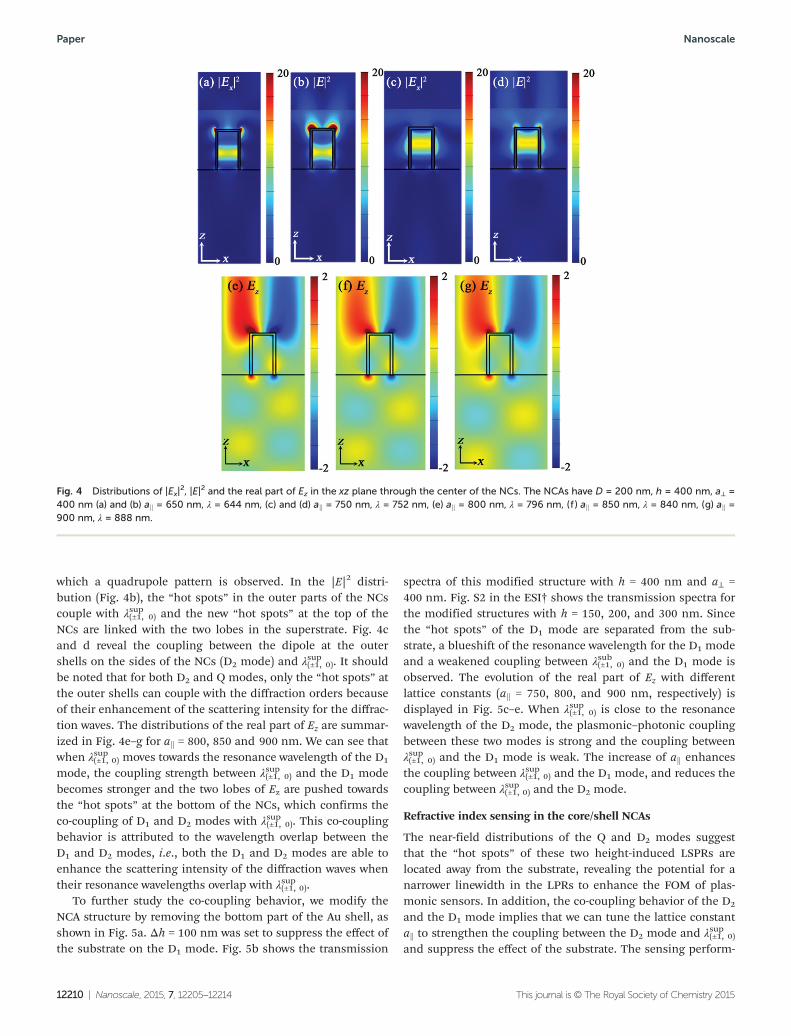
which a quadrupole pattern is observed. In the |E|2 distri-bution (Fig. 4b), the “hot spots” in the outer parts of the NCscouple with λsup(±1, 0) and the new “hot spots” at the top of theNCs are linked with the two lobes in the superstrate. Fig. 4cand d reveal the coupling between the dipole at the outershells on the sides of the NCs (D2 mode) and λsup(±1, 0). It shouldbe noted that for both D2 and Q modes, only the “hot spots” atthe outer shells can couple with the diffraction orders becauseof their enhancement of the scattering intensity for the diffrac-tion waves. The distributions of the real part of Ez are summar-ized in Fig. 4e–g for ak = 800, 850 and 900 nm. We can see thatwhen λsup(±1, 0) moves towards the resonance wavelength of the D1
mode, the coupling strength between λsup(±1, 0) and the D1 modebecomes stronger and the two lobes of Ez are pushed towardsthe “hot spots” at the bottom of the NCs, which confirms theco-coupling of D1 and D2 modes with λsup(±1, 0). This co-couplingbehavior is attributed to the wavelength overlap between theD1 and D2 modes, i.e., both the D1 and D2 modes are able toenhance the scattering intensity of the diffraction waves whentheir resonance wavelengths overlap with λsup(±1, 0).
To further study the co-coupling behavior, we modify theNCA structure by removing the bottom part of the Au shell, asshown in Fig. 5a. Δh = 100 nm was set to suppress the effect ofthe substrate on the D1 mode. Fig. 5b shows the transmission
spectra of this modified structure with h = 400 nm and a⊥ =400 nm. Fig. S2 in the ESI† shows the transmission spectra forthe modified structures with h = 150, 200, and 300 nm. Sincethe “hot spots” of the D1 mode are separated from the sub-strate, a blueshift of the resonance wavelength for the D1 modeand a weakened coupling between λsub(±1, 0) and the D1 mode isobserved. The evolution of the real part of Ez with differentlattice constants (ak = 750, 800, and 900 nm, respectively) isdisplayed in Fig. 5c–e. When λsup(±1, 0) is close to the resonancewavelength of the D2 mode, the plasmonic–photonic couplingbetween these two modes is strong and the coupling betweenλsup(±1, 0) and the D1 mode is weak. The increase of ak enhancesthe coupling between λsup(±1, 0) and the D1 mode, and reduces thecoupling between λsup(±1, 0) and the D2 mode.
Refractive index sensing in the core/shell NCAs
The near-field distributions of the Q and D2 modes suggestthat the “hot spots” of these two height-induced LSPRs arelocated away from the substrate, revealing the potential for anarrower linewidth in the LPRs to enhance the FOM of plas-monic sensors. In addition, the co-coupling behavior of the D2
and the D1 mode implies that we can tune the lattice constantak to strengthen the coupling between the D2 mode and λsup(±1, 0)
and suppress the effect of the substrate. The sensing perform-
Fig. 4 Distributions of |Ex|2, |E|2 and the real part of Ez in the xz plane through the center of the NCs. The NCAs have D = 200 nm, h = 400 nm, a⊥ =
400 nm (a) and (b) ak = 650 nm, λ = 644 nm, (c) and (d) ak = 750 nm, λ = 752 nm, (e) ak = 800 nm, λ = 796 nm, (f ) ak = 850 nm, λ = 840 nm, (g) ak =900 nm, λ = 888 nm.
Paper Nanoscale
12210 | Nanoscale, 2015, 7, 12205–12214 This journal is © The Royal Society of Chemistry 2015

ances based on the core/shell SiO2/Au NCAs are summarizedin Fig. 6. Firstly, we examine the sensing performance of theSiO2/Au NCAs with a low aspect ratio, which, however, couldbe optimized to achieve high FOM in a quasi-symmetricenvironment. We take the NCAs with h = 100 nm, a⊥ = 400 nm,and ak = 600 nm as an exemplary structure. Fig. 6a shows thetransmission spectra as a function of the superstrate refractiveindex, which ranges from 1.0 to 1.5. The D2 mode is weakwhen h = 100 nm (also see Fig. 3b). For a lower refractiveindex, λsup(±1, 0) is away from the resonance wavelength of the D1
mode and the coupling is also weak. However, when the refrac-tive index reaches 1.4, a narrow and sharp transmission dip isobserved. This resonance dip with a high quality factor isattributed to the wavelength matching between λsup(±1, 0) and theD1 mode in a quasi-symmetric environment. The FWHM of<10 nm is estimated based on the spectrum with a refractiveindex of 1.5. Considering that the refractive index ranges from1.4 to 1.5, a high FOM of 59 is achieved. This is consistentwith the previously reported LPR-based plasmonic sensors,which exhibited high FOMs when the refractive index of thetarget analyte was close to that of the substrate. However, thecore/shell SiO2/Au NCAs show a much higher FOM than thatreported in the square or hexagonal Au nanoparticlearrays.44,48 It should be noted that LPR is a coupling mode,which requires a good wavelength matching between the
LSPRs and the diffraction orders to achieve a high qualityfactor. Since the wavelength sensitivity of the LSPRs to therefractive index of the target analyte is quite different fromthat of the diffraction orders, the change of the refractive indexwill lead to a deviation between the plasmonic mode and thephotonic mode, resulting in a weak coupling and a low FOM.This explains why the detected range of the analyte refractiveindex is limited in the conventional LPR-based plasmonicsensors. To our benefit, optimization of the aspect ratio in thecore/shell NCAs provides a mechanism to maintain the highFOM for a wide range of the analyte refractive indices.
Fig. 6b shows the sensing performance of the core/shellNCAs with a⊥ = 400 nm, ak = 650 nm, and h = 400 nm. Com-pared with the results in the Au NDAs, a narrower linewidthand a concomitant higher FOM are obtained. To clearlydemonstrate the spectral shift of the LPR dips, we have plottedthe normalized transmission spectra in Fig. 6c. As shown inFig. 3e, λsup(±1, 0) is able to couple with the Q, D1 and D2 modes,respectively, when it crosses over the spectral region of theseLSPRs. This is the basic concept we employ to maintain thehigh FOM over a wide range of analyte refractive index. Thenarrow linewidth at around 700 nm indicates the couplingbetween λsup(±1, 0) and the Q mode. The linewidth at a refractiveindex of 1.1 is much broader than that in other transmissiondips because λsup(±1, 0) at 715 nm weakly couples with the Q mode
Fig. 5 (a) Cross section of the modified core/shell NC with the bottom part of the Au nanoshell removed, the distance between the bottom of theAu nanoshell and the SiO2 substrate is indicated as Δh, which is 100 nm. (b) Transmission spectra of the modified NCAs as a function of ak. The NCAshave D = 200 nm, h = 400 nm and a⊥ = 400 nm. (c)–(e) Distributions of the real part of Ez in the xz plane through the center of the NCs. The NCAshave (c) ak = 750 nm, λ = 752 nm, (d) ak = 800 nm, λ = 796 nm, (e) ak = 900 nm, λ = 880 nm.
Nanoscale Paper
This journal is © The Royal Society of Chemistry 2015 Nanoscale, 2015, 7, 12205–12214 | 12211
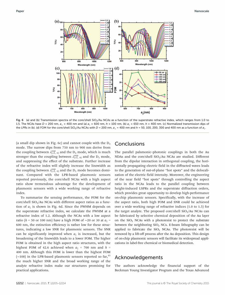
(a small dip shown in Fig. 6c) and cannot couple with the D2
mode. The narrow dips from 750 nm to 900 nm derive fromthe coupling between λsup(±1, 0) and the D2 mode, which is muchstronger than the coupling between λsup(±1, 0) and the D1 mode,and suppressing the effect of the substrate. Further increaseof the refractive index will slightly increase the linewidth asthe coupling between λsup(±1, 0) and the D1 mode becomes domi-nant. Compared with the LPR-based plasmonic sensorsreported previously, the core/shell NCAs with a high aspectratio show tremendous advantage for the development ofplasmonic sensors with a wide working range of refractiveindex.
To summarize the sensing performance, the FOM for thecore/shell SiO2/Au NCAs with different aspect ratios as a func-tion of ak is shown in Fig. 6d. Since the FWHM depends onthe superstrate refractive index, we calculate the FWHM at arefractive index of 1.2. Although the NCAs with a low aspectratio (h = 50 or 100 nm) have a high FOM of ∼20 or 30 at ak =600 nm, the extinction efficiency is rather low for these struc-tures, indicating a low SNR for plasmonic sensors. The SNRcan be significantly improved when ak is increased, but thebroadening of the linewidth leads to a lower FOM. The higherFOM is obtained in the high aspect ratio structures, with thehighest FOM of 42.6 achieved when ak = 700 nm and h =400 nm. Although this FOM is lower than the highest FOM(∼108) in the LPR-based plasmonic sensors reported so far,45
the much higher SNR and the broad working range of theanalyte refractive index make our structures promising forpractical applications.
Conclusions
The parallel palsmonic–photonic couplings in both the AuNDAs and the core/shell SiO2/Au NCAs are studied. Differentfrom the dipolar interaction in orthogonal coupling, the hori-zontally propagating electric field in the diffracted waves leadsto the generation of out-of-plane “hot spots” and the delocali-zation of the electric field intensity. Moreover, the engineeringof the near field “hot spots” through controlling the aspectratio in the NCAs leads to the parallel coupling betweenheight-induced LSPRs and the superstrate diffraction orders,which provides great opportunity to develop high-performanceon-chip plasmonic sensors. Specifically, with the increase ofthe aspect ratio, both high FOM and SNR could be achievedover a wide working range of refractive indices (1.0 to 1.5) forthe target analyte. The proposed core/shell SiO2/Au NCAs canbe fabricated by selective chemical deposition of the Au layeron the SiO2 NCAs with a photoresist to protect the substratebetween the neighboring SiO2 NCs. E-beam lithography can beapplied to fabricate the SiO2 NCAs. The photoresist will beremoved by a lift-off process after the Au deposition. This designof on-chip plasmonic sensors will facilitate its widespread appli-cations in label-free chemical or biomedical detection.
Acknowledgements
The authors acknowledge the financial support of theBeckman Young Investigator Program and the Texas Advanced
Fig. 6 (a) and (b) Transmission spectra of the core/shell SiO2/Au NCAs as a function of the superstrate refractive index, which ranges from 1.0 to1.5. The NCAs have D = 200 nm, a⊥ = 400 nm and (a) ak = 600 nm, h = 100 nm, (b) ak = 650 nm, h = 400 nm. (c) Normalized transmission dips ofthe LPRs in (b). (d) FOM for the core/shell SiO2/Au NCAs with D = 200 nm, a⊥ = 400 nm and h = 50, 100, 200, 300 and 400 nm as a function of ak.
Paper Nanoscale
12212 | Nanoscale, 2015, 7, 12205–12214 This journal is © The Royal Society of Chemistry 2015
Computing Center (TACC) at The University of Texas at Austinfor providing HPC resources that have contributed to theresearch results reported within this paper. URL: http://www.tacc.utexas.edu. We thank B. Bangalore Rajeeva, X. Peng,M. Wang, and Z. Wu for helpful discussions on the simulationresults and proofreading the manuscript.
Notes and references
1 K. Tanaka, E. Plum, J. Y. Ou, T. Uchino and N. I. Zheludev,Phys. Rev. Lett., 2010, 105, 227403.
2 N. Gandra, C. Portz, L. Tian, R. Tang, B. Xu, S. Achilefu andS. Singamaneni, Angew. Chem., Int. Ed., 2014, 53, 866–870.
3 D. Lu, J. J. Kan, E. E. Fullerton and Z. Liu, Nat. Nanotech-nol., 2014, 9, 48–53.
4 X. Dang, J. Qi, M. T. Klug, P.-Y. Chen, D. S. Yun, N. X. Fang,P. T. Hammond and A. M. Belcher, Nano Lett., 2013, 13,637–642.
5 O. Neumann, C. Feronti, A. D. Neumann, A. Dong,K. Schell, B. Lu, E. Kim, M. Quinn, S. Thompson, N. Grady,P. Nordlander, M. Oden and N. J. Halas, Proc. Natl. Acad.Sci. U. S. A., 2013, 110, 11677–11681.
6 S. Mubeen, J. Lee, W.-r. Lee, N. Singh, G. D. Stucky andM. Moskovits, ACS Nano, 2014, 8, 6066–6073.
7 H. A. Atwater and A. Polman, Nat. Mater., 2010, 9, 205–213.8 Y. B. Zheng, B. Kiraly, P. S. Weiss and T. J. Huang, Nano-
medicine, 2012, 7, 751–770.9 Y. B. Zheng, J. L. Payton, T.-B. Song, B. K. Pathem, Y. Zhao,
H. Ma, Y. Yang, L. Jensen, A. K. Y. Jen and P. S. Weiss, NanoLett., 2012, 12, 5362–5368.
10 L. Scarabelli, M. Coronado-Puchau, J. J. Giner-Casares,J. Langer and L. M. Liz-Marzán, ACS Nano, 2014, 8, 5833–5842.
11 K. A. Willets and R. P. Van Duyne, Annu. Rev. Phys. Chem.,2007, 58, 267–297.
12 C. Zhao, Y. Liu, J. Yang and J. Zhang, Nanoscale, 2014, 6,9103–9109.
13 L. L. Zhao, L. Jensen and G. C. Schatz, Nano Lett., 2006, 6,1229–1234.
14 W. Wan, W. Zheng, Y. Chen and Z. Liu, Nanoscale, 2014, 6,9093–9102.
15 L. Shao, Q. Ruan, R. Jiang and J. Wang, Small, 2014, 10,802–811.
16 L. Tong, H. Wei, S. Zhang and H. Xu, Sensors, 2014, 14,7959–7973.
17 H. Wei and H. Xu, Nanoscale, 2013, 5, 10794–10805.18 R. Bardhan, S. Lal, A. Joshi and N. J. Halas, Acc. Chem. Res.,
2011, 44, 936–946.19 C. Ayala-Orozco, C. Urban, M. W. Knight, A. S. Urban,
O. Neumann, S. W. Bishnoi, S. Mukherjee, A. M. Goodman,H. Charron, T. Mitchell, M. Shea, R. Roy, S. Nanda,R. Schiff, N. J. Halas and A. Joshi, ACS Nano, 2014, 8, 6372–6381.
20 T. Klar, M. Perner, S. Grosse, G. von Plessen, W. Spirkl andJ. Feldmann, Phys. Rev. Lett., 1998, 80, 4249–4252.
21 R. Bukasov, T. A. Ali, P. Nordlander and J. S. Shumaker-Parry, ACS Nano, 2010, 4, 6639–6650.
22 N. J. Halas, S. Lal, W. S. Chang, S. Link and P. Nordlander,Chem. Rev., 2011, 111, 3913–3961.
23 K. H. Fung, A. Kumar and N. X. Fang, Phys. Rev. B: Condens.Matter, 2014, 89, 045408.
24 E. Prodan, C. Radloff, N. J. Halas and P. Nordlander,Science, 2003, 302, 419–422.
25 B. Auguie and W. L. Barnes, Phys. Rev. Lett., 2008, 101,143902.
26 Y. Chu, E. Schonbrun, T. Yang and K. B. Crozier, Appl. Phys.Lett., 2008, 93, 181108.
27 V. G. Kravets, F. Schedin and A. N. Grigorenko, Phys. Rev.Lett., 2008, 101, 087403.
28 H. Gao, J. M. McMahon, M. H. Lee, J. Henzie, S. K. Gray,G. C. Schatz and T. W. Odom, Opt. Express, 2009, 17, 2334–2340.
29 A. Vitrey, L. Aigouy, P. Prieto, J. M. García-Martín andM. U. González, Nano Lett., 2014, 14, 2079–2085.
30 A. G. Nikitin, T. Nguyen and H. Dallaporta, Appl. Phys. Lett.,2013, 102, 221116.
31 A. G. Nikitin, Appl. Phys. Lett., 2014, 104, 061107.32 L. Lin and Y. Yi, Opt. Lett., 2014, 39, 4823–4826.33 L. Lin and Y. Zheng, Opt. Lett., 2015, 40, 2060–2063.34 V. A. Markel, J. Mod. Opt., 1993, 40, 2281–2291.35 S. L. Zou, N. Janel and G. C. Schatz, J. Chem. Phys., 2004,
120, 10871–10875.36 S. L. Zou and G. C. Schatz, J. Chem. Phys., 2004, 121,
12606–12612.37 V. A. Markel, J. Phys. B: At., Mol. Opt. Phys., 2005, 38, L115–
L121.38 M. Meier, A. Wokaun and P. F. Liao, J. Opt. Soc. Am. B,
1985, 2, 931–949.39 L. L. Zhao, K. L. Kelly and G. C. Schatz, J. Phys. Chem. B,
2003, 107, 7343–7350.40 J. Y. Suh, C. H. Kim, W. Zhou, M. D. Huntington, D. T. Co,
M. R. Wasielewski and T. W. Odom, Nano Lett., 2012, 12,5769–5774.
41 F. van Beijnum, P. J. van Veldhoven, E. J. Geluk, M. J. A. deDood, G. W. t. Hooft and M. P. van Exter, Phys. Rev. Lett.,2013, 110, 206802.
42 W. Zhou, M. Dridi, J. Y. Suh, C. H. Kim, D. T. Co,M. R. Wasielewski, G. C. Schatz and T. W. Odom, Nat.Nanotechnol., 2013, 8, 506–511.
43 J. Henzie, M. H. Lee and T. W. Odom, Nat. Nanotechnol.,2007, 2, 549–554.
44 A. I. Kuznetsov, A. B. Evlyukhin, M. R. Goncalves,C. Reinhardt, A. Koroleva, M. L. Arnedillo, R. Kiyan,O. Marti and B. N. Chichkov, ACS Nano, 2011, 5, 4843–4849.
45 Y. Shen, J. Zhou, T. Liu, Y. Tao, R. Jiang, M. Liu, G. Xiao,J. Zhu, Z.-K. Zhou, X. Wang, C. Jin and J. Wang, Nat.Commun., 2013, 4, 2381.
46 B. Spackova and J. Homola, Opt. Express, 2013, 21, 27490–27502.
47 Y. Du, L. Shi, M. Hong, H. Li, D. Li and M. Liu, Opt.Commun., 2013, 298, 232–236.
Nanoscale Paper
This journal is © The Royal Society of Chemistry 2015 Nanoscale, 2015, 7, 12205–12214 | 12213

48 P. Offermans, M. C. Schaafsma, S. R. K. Rodriguez,Y. Zhang, M. Crego-Calama, S. H. Brongersma andJ. G. Rivas, ACS Nano, 2011, 5, 5151–5157.
49 B. Auguie, X. M. Bendana, W. L. Barnes and F. J. Garcia deAbajo, Phys. Rev. B: Condens. Matter, 2010, 82,155447.
50 K. M. Mayer and J. H. Hafner, Chem. Rev., 2011, 111, 3828–3857.
51 K. A. Tetz, L. Pang and Y. Fainman, Opt. Lett., 2006, 31,1528–1530.
52 L. Lin and Y. Yi, Opt. Express, 2015, 23, 130–142.53 L. J. Sherry, S. H. Chang, G. C. Schatz, R. P. Van Duyne,
B. J. Wiley and Y. N. Xia, Nano Lett., 2005, 5, 2034–2038.54 A. Dmitriev, C. Hägglund, S. Chen, H. Fredriksson,
T. Pakizeh, M. Käll and D. S. Sutherland, Nano Lett., 2008,8, 3893–3898.
Paper Nanoscale
12214 | Nanoscale, 2015, 7, 12205–12214 This journal is © The Royal Society of Chemistry 2015