cache memory cse 675.02 slides from dan garcia, ucb
TRANSCRIPT

Cache Memory
CSE 675.02
Slides from Dan Garcia, UCB

The Big Picture
Processor (active)
Computer
Control(“brain”)Datapath(“brawn”)
Memory(passive)(where programs, data live whenrunning)
DevicesInput
Output
Keyboard, Mouse
Display, Printer
Disk,Network

Memory Hierarchy (1/3)
•Processor• executes instructions on order of nanoseconds to picoseconds
• holds a small amount of code and data in registers
•Memory• More capacity than registers, still limited
• Access time ~50-100 ns
•Disk• HUGE capacity (virtually limitless)• VERY slow: runs ~milliseconds

The Levels in Memory Hierarchy
• Higher the level, smaller and faster the memory. • Try to keep most of the action in the higher levels.
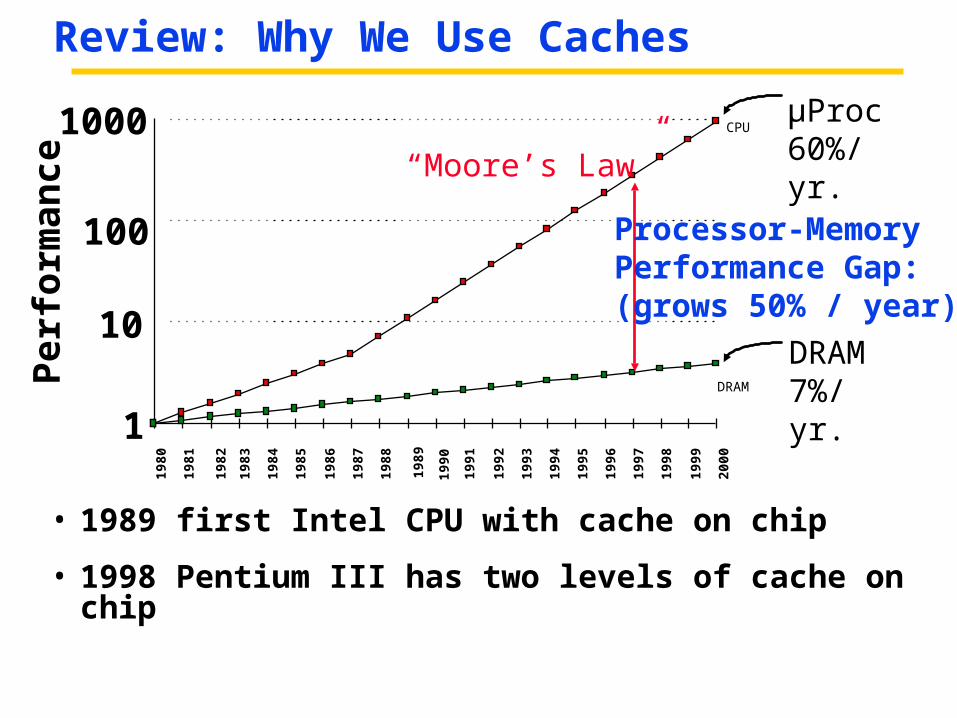
Review: Why We Use Caches
µProc60%/yr.
DRAM7%/yr.
1
10
100
10001980
1981
1983
1984
1985
1986
1987
1988
1989
1990
1991
1992
1993
1994
1995
1996
1997
1998
1999
2000
DRAM
CPU
1982
Processor-MemoryPerformance Gap:(grows 50% / year)
Per
form
ance “Moore’s Law”
• 1989 first Intel CPU with cache on chip
• 1998 Pentium III has two levels of cache on chip

Memory Hierarchy (2/3) Processor
Size of memory at each level
Increasing Distance
from Proc.,Decreasing
speed
Level 1
Level 2
Level n
Level 3
. . .
Higher
Lower
Levels in memory
hierarchy
As we move to deeper levels the latency goes up and price per bit goes down.
Q: Can $/bit go up as move deeper?

Memory Hierarchy (3/3)• If level closer to Processor, it must be:
• smaller
• faster
• subset of lower levels (contains most recently used data)
•Lowest Level (usually disk) contains all available data
•Other levels?

Memory Caching
•We’ve discussed three levels in the hierarchy: processor, memory, disk
•Mismatch between processor and memory speeds leads us to add a new level: a memory cache
• Implemented with SRAM technology: faster but more expensive than DRAM memory.
• “S” = Static, no need to refresh, ~10ns
• “D” = Dynamic, need to refresh, ~60ns• arstechnica.com/paedia/r/ram_guide/ram_guide.part1-1.html

Memory Hierarchy Analogy: Library (1/2)•You’re writing a term paper (Processor) at a table in SEL
•SEL Library is equivalent to disk• essentially limitless capacity
• very slow to retrieve a book
•Table is memory• smaller capacity: means you must return book when table fills up
• easier and faster to find a book there once you’ve already retrieved it

Memory Hierarchy Analogy: Library (2/2)•Open books on table are cache
• smaller capacity: can have very few open books fit on table; again, when table fills up, you must close a book
• much, much faster to retrieve data
• Illusion created: whole library open on the tabletop
• Keep as many recently used books open on table as possible since likely to use again
• Also keep as many books on table as possible, since faster than going to library
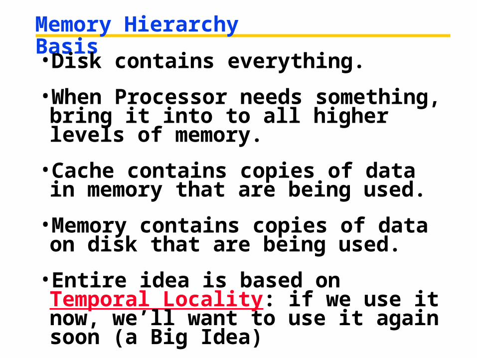
Memory Hierarchy Basis•Disk contains everything.
•When Processor needs something, bring it into to all higher levels of memory.
•Cache contains copies of data in memory that are being used.
•Memory contains copies of data on disk that are being used.
•Entire idea is based on Temporal Locality: if we use it now, we’ll want to use it again soon (a Big Idea)

Cache Design•How do we organize cache?
•Where does each memory address map to?
(Remember that cache is subset of memory, so multiple memory addresses map to the same cache location.)
•How do we know which elements are in cache?
•How do we quickly locate them?

Direct-Mapped Cache (1/2)• In a direct-mapped cache, each memory address is associated with one possible block within the cache
• Therefore, we only need to look in a single location in the cache for the data if it exists in the cache
• Block is the unit of transfer between cache and memory
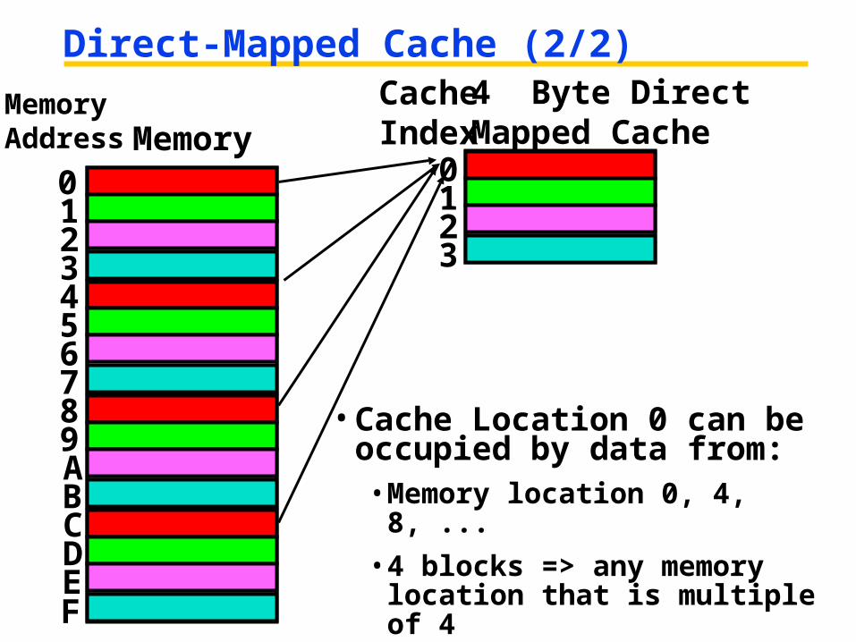
Direct-Mapped Cache (2/2)
• Cache Location 0 can be occupied by data from:• Memory location 0, 4, 8, ...
• 4 blocks => any memory location that is multiple of 4
MemoryMemory Address
0123456789ABCDEF
4 Byte Direct Mapped Cache
Cache Index
0123
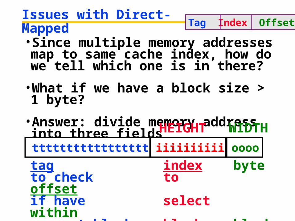
Issues with Direct-Mapped•Since multiple memory addresses map to same cache index, how do we tell which one is in there?
•What if we have a block size > 1 byte?
•Answer: divide memory address into three fields
ttttttttttttttttt iiiiiiiiii oooo
tag index byteto check to offsetif have select withincorrect block block block
WIDTHHEIGHT
Tag Index Offset
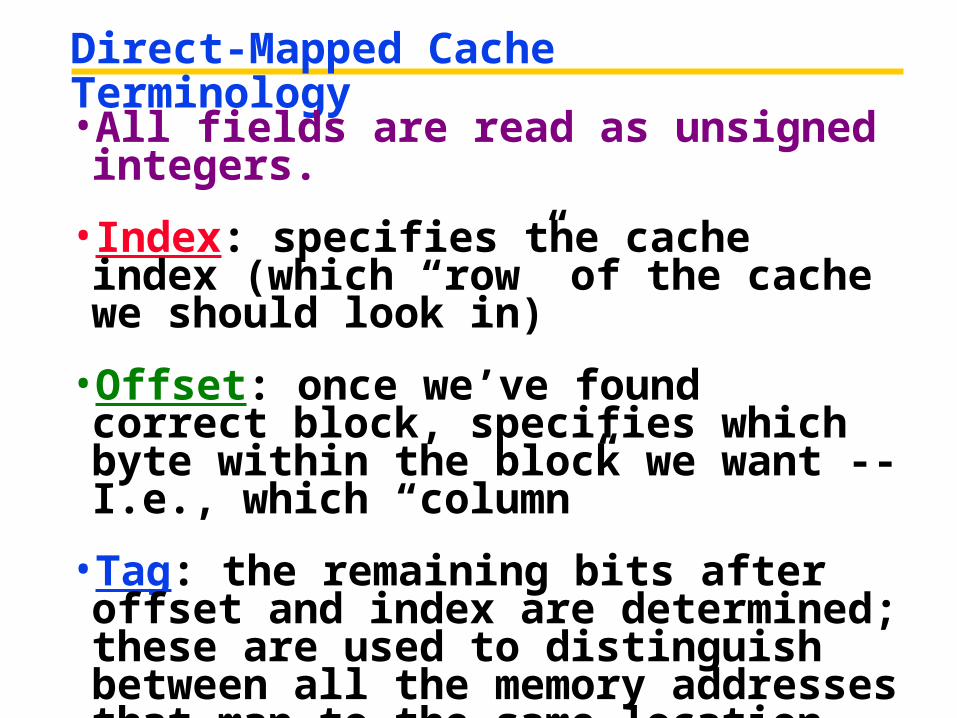
Direct-Mapped Cache Terminology•All fields are read as unsigned integers.
• Index: specifies the cache index (which “row” of the cache we should look in)
•Offset: once we’ve found correct block, specifies which byte within the block we want -- I.e., which “column”
•Tag: the remaining bits after offset and index are determined; these are used to distinguish between all the memory addresses that map to the same location

TIO Dan’s great cache mnemonic
AREA (cache size, B)= HEIGHT (# of blocks) * WIDTH (size of one block, B/block)
WIDTH (size of one block, B/block)
HEIGHT(# of blocks)
AREA(cache size, B)
2(H+W) = 2H * 2W
Tag Index Offset
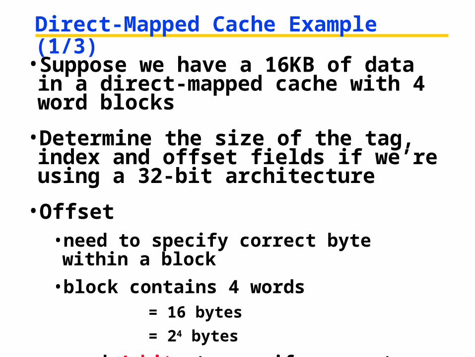
Direct-Mapped Cache Example (1/3)•Suppose we have a 16KB of data in a direct-mapped cache with 4 word blocks
•Determine the size of the tag, index and offset fields if we’re using a 32-bit architecture
•Offset• need to specify correct byte within a block
• block contains 4 words = 16 bytes
= 24 bytes
• need 4 bits to specify correct byte

Direct-Mapped Cache Example (2/3)• Index: (~index into an “array of blocks”)
• need to specify correct row in cache
• cache contains 16 KB = 214 bytes
• block contains 24 bytes (4 words)
• # blocks/cache = bytes/cache
bytes/block
= 214 bytes/cache 24 bytes/block
= 210 blocks/cache
• need 10 bits to specify this many rows

Direct-Mapped Cache Example (3/3)•Tag: use remaining bits as tag• tag length = addr length - offset - index
= 32 - 4 - 10 bits = 18 bits
• so tag is leftmost 18 bits of memory address
•Why not full 32 bit address as tag?• All bytes within block need same address (4b)
• Index must be same for every address within a block, so its redundant in tag check, thus can leave off to save memory (10 bits in this example)

Caching Terminology• When we try to read memory,
3 things can happen:
1. cache hit: cache block is valid and contains proper address, so read desired word
2. cache miss: nothing in cache in appropriate block, so fetch from memory
3. cache miss, block replacement: wrong data is in cache at appropriate block, so discard it and fetch desired data from memory (cache always copy)

Accessing data in a direct mapped cache• Ex.: 16KB of data, direct-mapped, 4 word blocks
• Read 4 addresses1. 0x000000142. 0x0000001C3. 0x000000344. 0x00008014
• Memory values on right:
• only cache/ memory level of hierarchy
Address (hex)Value of WordMemory
0000001000000014000000180000001C
abcd
... ...
0000003000000034000000380000003C
efgh
0000801000008014000080180000801C
ijkl
... ...
... ...
... ...

Accessing data in a direct mapped cache•4 Addresses:•0x00000014, 0x0000001C, 0x00000034, 0x00008014
•4 Addresses divided (for convenience) into Tag, Index, Byte Offset fields
000000000000000000 0000000001 0100
000000000000000000 0000000001 1100
000000000000000000 0000000011 0100
000000000000000010 0000000001 0100
Tag Index Offset
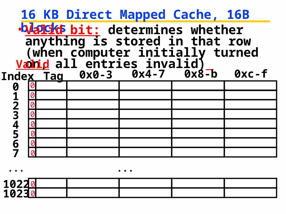
16 KB Direct Mapped Cache, 16B blocks• Valid bit: determines whether anything is stored in that row (when computer initially turned on, all entries invalid)
...
ValidTag 0x0-3 0x4-7 0x8-b 0xc-f
01234567
10221023
...
Index00000000
00
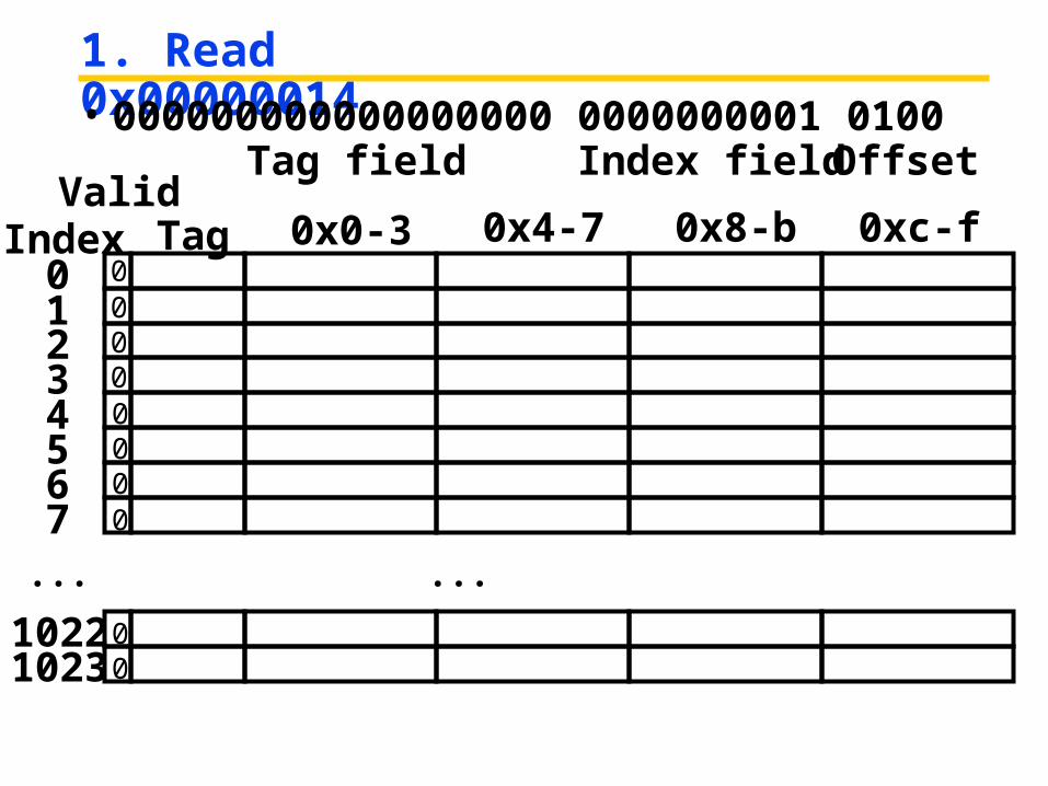
1. Read 0x00000014
...
ValidTag 0x0-3 0x4-7 0x8-b 0xc-f
01234567
10221023
...
• 000000000000000000 0000000001 0100
Index
Tag field Index field Offset
00000000
00

So we read block 1 (0000000001)
...
ValidTag 0x0-3 0x4-7 0x8-b 0xc-f
01234567
10221023
...
• 000000000000000000 0000000001 0100
Index
Tag field Index field Offset
00000000
00
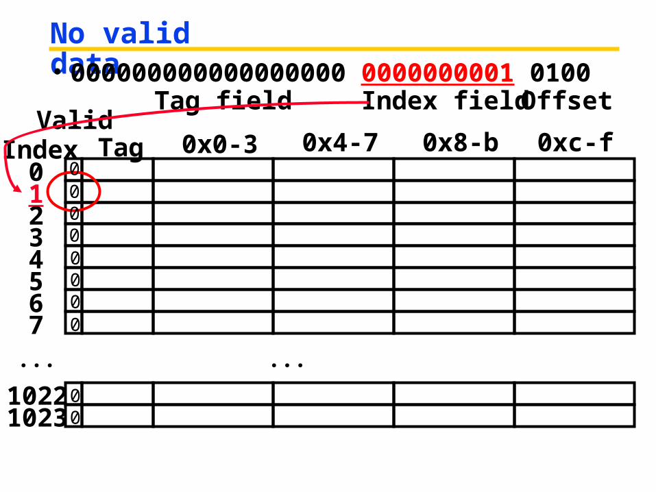
No valid data
...
ValidTag 0x0-3 0x4-7 0x8-b 0xc-f
01234567
10221023
...
• 000000000000000000 0000000001 0100
Index
Tag field Index field Offset
00000000
00

So load that data into cache, setting tag, valid
...
ValidTag 0x0-3 0x4-7 0x8-b 0xc-f
01234567
10221023
...
1 0 a b c d
• 000000000000000000 0000000001 0100
Index
Tag field Index field Offset
0
000000
00
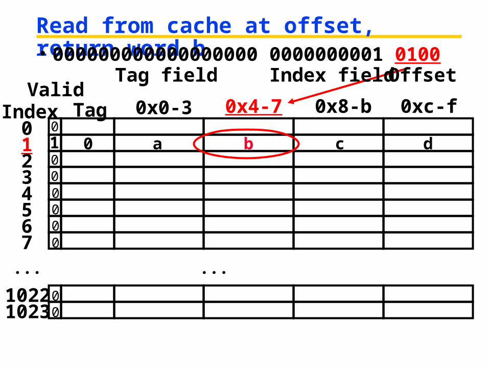
Read from cache at offset, return word b• 000000000000000000 0000000001 0100
...
ValidTag 0x0-3 0x4-7 0x8-b 0xc-f
01234567
10221023
...
1 0 a b c d
Index
Tag field Index field Offset
0
000000
00

2. Read 0x0000001C = 0…00 0..001 1100
...
ValidTag 0x0-3 0x4-7 0x8-b 0xc-f
01234567
10221023
...
1 0 a b c d
• 000000000000000000 0000000001 1100
Index
Tag field Index field Offset
0
000000
00

Index is Valid
...
ValidTag 0x0-3 0x4-7 0x8-b 0xc-f
01234567
10221023
...
1 0 a b c d
• 000000000000000000 0000000001 1100
Index
Tag field Index field Offset
0
000000
00

Index valid, Tag Matches
...
ValidTag 0x0-3 0x4-7 0x8-b 0xc-f
01234567
10221023
...
1 0 a b c d
• 000000000000000000 0000000001 1100
Index
Tag field Index field Offset
0
000000
00

Index Valid, Tag Matches, return d
...
ValidTag 0x0-3 0x4-7 0x8-b 0xc-f
01234567
10221023
...
1 0 a b c d
• 000000000000000000 0000000001 1100
Index
Tag field Index field Offset
0
000000
00

3. Read 0x00000034 = 0…00 0..011 0100
...
ValidTag 0x0-3 0x4-7 0x8-b 0xc-f
01234567
10221023
...
1 0 a b c d
• 000000000000000000 0000000011 0100
Index
Tag field Index field Offset
0
000000
00
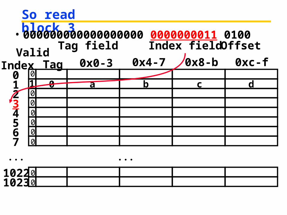
So read block 3
...
ValidTag 0x0-3 0x4-7 0x8-b 0xc-f
01234567
10221023
...
1 0 a b c d
• 000000000000000000 0000000011 0100
Index
Tag field Index field Offset
0
000000
00

No valid data
...
ValidTag 0x0-3 0x4-7 0x8-b 0xc-f
01234567
10221023
...
1 0 a b c d
• 000000000000000000 0000000011 0100
Index
Tag field Index field Offset
0
000000
00

Load that cache block, return word f
...
ValidTag 0x0-3 0x4-7 0x8-b 0xc-f
01234567
10221023
...
1 0 a b c d
• 000000000000000000 0000000011 0100
1 0 e f g h
Index
Tag field Index field Offset
0
0
0000
00

4. Read 0x00008014 = 0…10 0..001 0100
...
ValidTag 0x0-3 0x4-7 0x8-b 0xc-f
01234567
10221023
...
1 0 a b c d
• 000000000000000010 0000000001 0100
1 0 e f g h
Index
Tag field Index field Offset
0
0
0000
00

So read Cache Block 1, Data is Valid
...
ValidTag 0x0-3 0x4-7 0x8-b 0xc-f
01234567
10221023
...
1 0 a b c d
• 000000000000000010 0000000001 0100
1 0 e f g h
Index
Tag field Index field Offset
0
0
0000
00

Cache Block 1 Tag does not match (0 != 2)
...
ValidTag 0x0-3 0x4-7 0x8-b 0xc-f
01234567
10221023
...
1 0 a b c d
• 000000000000000010 0000000001 0100
1 0 e f g h
Index
Tag field Index field Offset
0
0
0000
00

Miss, so replace block 1 with new data & tag
...
ValidTag 0x0-3 0x4-7 0x8-b 0xc-f
01234567
10221023
...
1 2 i j k l
• 000000000000000010 0000000001 0100
1 0 e f g h
Index
Tag field Index field Offset
0
0
0000
00
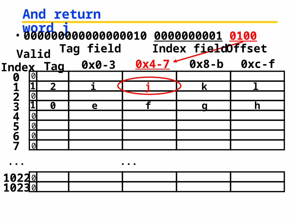
And return word j
...
ValidTag 0x0-3 0x4-7 0x8-b 0xc-f
01234567
10221023
...
1 2 i j k l
• 000000000000000010 0000000001 0100
1 0 e f g h
Index
Tag field Index field Offset
0
0
0000
00
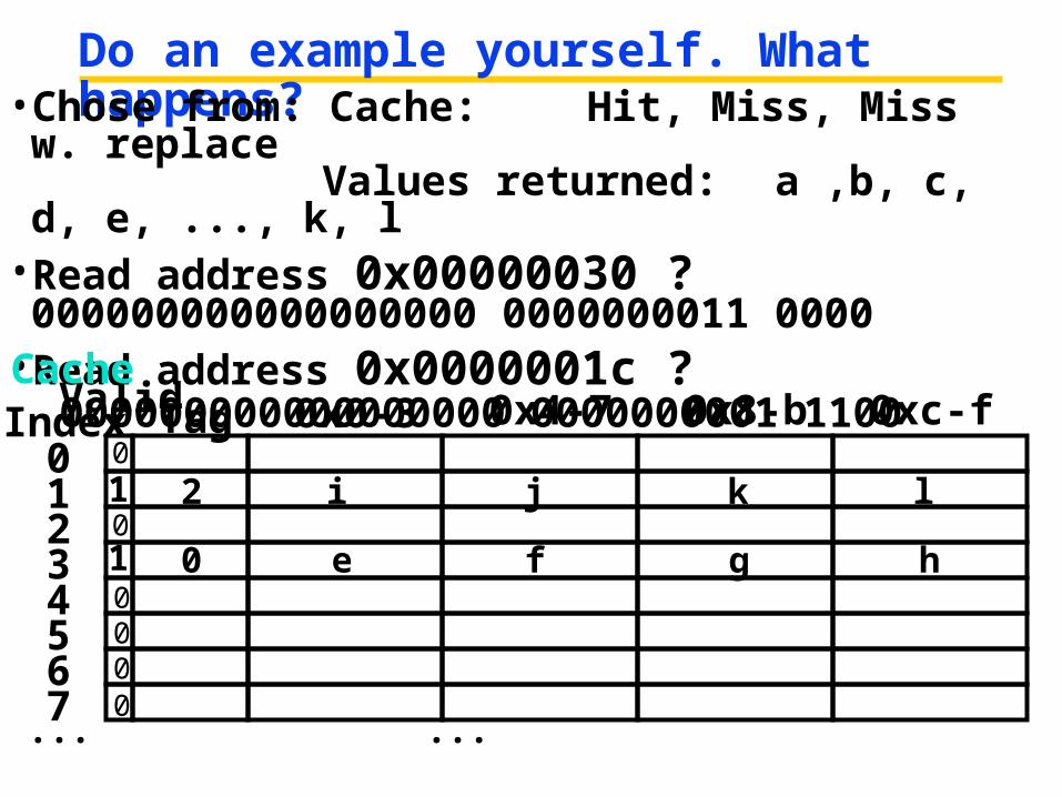
Do an example yourself. What happens?• Chose from: Cache: Hit, Miss, Miss w. replace
Values returned: a ,b, c, d, e, ..., k, l• Read address 0x00000030 ? 000000000000000000 0000000011 0000• Read address 0x0000001c ? 000000000000000000 0000000001 1100
...
ValidTag 0x0-3 0x4-7 0x8-b 0xc-f01234567...
1 2 i j k l
1 0 e f g h
Index0
0
0000
Cache
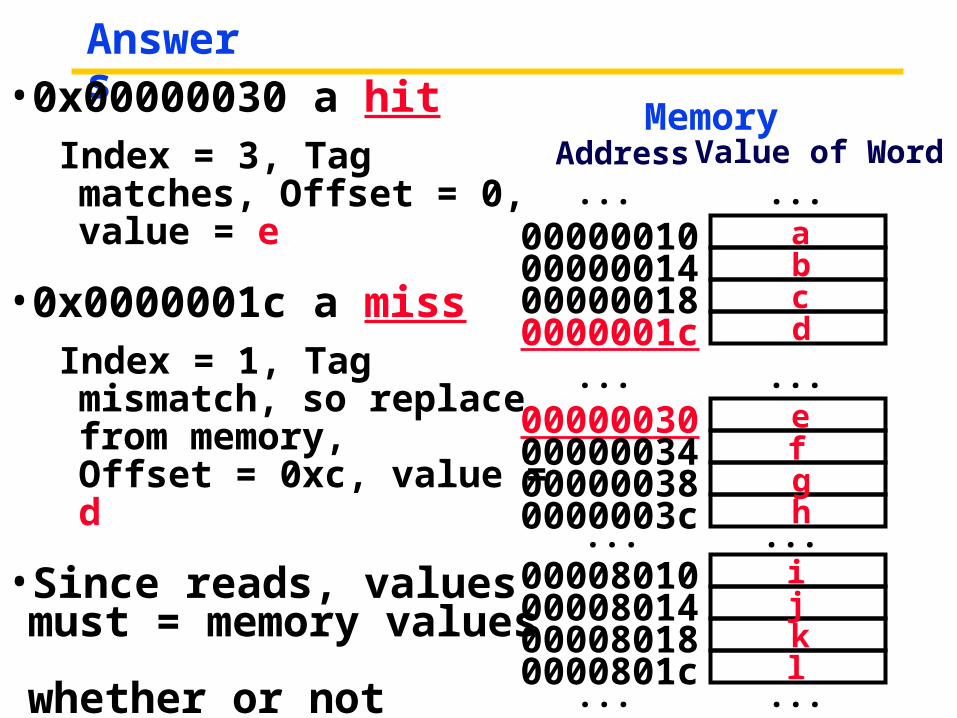
Answers•0x00000030 a hit
Index = 3, Tag matches, Offset = 0, value = e
•0x0000001c a missIndex = 1, Tag mismatch, so replace from memory, Offset = 0xc, value = d
•Since reads, values must = memory values whether or not cached:
• 0x00000030 = e
• 0x0000001c = d
Address Value of WordMemory
0000001000000014000000180000001c
abcd
... ...
0000003000000034000000380000003c
efgh
0000801000008014000080180000801c
ijkl
... ...
... ...
... ...

Peer Instruction
A. Mem hierarchies were invented before 1950. (UNIVAC I wasn’t delivered ‘til 1951)
B. If you know your computer’s cache size, you can often make your code run faster.
C. Memory hierarchies take advantage of spatial locality by keeping the most recent data items closer to the processor.
ABC1: FFF2: FFT3: FTF4: FTT5: TFF6: TFT7: TTF8: TTT

Peer Instructions
1. All caches take advantage of spatial locality.
2. All caches take advantage of temporal locality.
3. On a read, the return value will depend on what is in the cache.
ABC1: FFF2: FFT3: FTF4: FTT5: TFF6: TFT7: TTF8: TTT

And in Conclusion (1/2)•We would like to have the capacity of disk at the speed of the processor: unfortunately this is not feasible.
•So we create a memory hierarchy:• each successively lower level contains “most used” data from next higher level
• exploits temporal locality
• do the common case fast, worry less about the exceptions (design principle of MIPS)
•Locality of reference is a Big Idea

And in Conclusion (2/2)
•Mechanism for transparent movement of data among levels of a storage hierarchy
• set of address/value bindings• address index to set of candidates• compare desired address with tag• service hit or miss
- load new block and binding on miss
ValidTag 0x0-3 0x4-7 0x8-b 0xc-f
0123...
1 0 a b c d
000000000000000000 0000000001 1100address: tag index offset

Block Size Tradeoff (1/3)•Benefits of Larger Block Size
• Spatial Locality: if we access a given word, we’re likely to access other nearby words soon
• Very applicable with Stored-Program Concept: if we execute a given instruction, it’s likely that we’ll execute the next few as well
• Works nicely in sequential array accesses too

Block Size Tradeoff (2/3)• Drawbacks of Larger Block Size
• Larger block size means larger miss penalty- on a miss, takes longer time to load a new block from
next level
• If block size is too big relative to cache size, then there are too few blocks
- Result: miss rate goes up
• In general, minimize Average Memory Access Time (AMAT)
= Hit Time + Miss Penalty x Miss Rate

Block Size Tradeoff (3/3)•Hit Time = time to find and retrieve data from current level cache
•Miss Penalty = average time to retrieve data on a current level miss (includes the possibility of misses on successive levels of memory hierarchy)
•Hit Rate = % of requests that are found in current level cache
•Miss Rate = 1 - Hit Rate

Extreme Example: One Big Block
•Cache Size = 4 bytes Block Size = 4 bytes• Only ONE entry in the cache!
• If item accessed, likely accessed again soon• But unlikely will be accessed again immediately!
•The next access will likely to be a miss again• Continually loading data into the cache butdiscard data (force out) before use it again
• Nightmare for cache designer: Ping Pong Effect
Cache DataValid BitB 0B 1B 3
TagB 2

Block Size Tradeoff ConclusionsMissPenalty
Block Size
Increased Miss Penalty& Miss Rate
AverageMemoryAccess
Time
Block Size
Exploits Spatial Locality
Fewer blocks: compromisestemporal locality
MissRate
Block Size

Types of Cache Misses (1/2)
•“Three Cs” Model of Misses
•1st C: Compulsory Misses• occur when a program is first started
• cache does not contain any of that program’s data yet, so misses are bound to occur
• can’t be avoided easily, so won’t focus on these in this course

Types of Cache Misses (2/2)• 2nd C: Conflict Misses
• miss that occurs because two distinct memory addresses map to the same cache location
• two blocks (which happen to map to the same location) can keep overwriting each other
• big problem in direct-mapped caches
• how do we lessen the effect of these?
• Dealing with Conflict Misses• Solution 1: Make the cache size bigger
- Fails at some point
• Solution 2: Multiple distinct blocks can fit in the same cache Index?

Fully Associative Cache (1/3)•Memory address fields:
• Tag: same as before
• Offset: same as before
• Index: non-existant
•What does this mean?• no “rows”: any block can go anywhere in the cache
• must compare with all tags in entire cache to see if data is there

Fully Associative Cache (2/3)•Fully Associative Cache (e.g., 32 B block)
• compare tags in parallel
Byte Offset
:
Cache Data
B 0
0431
:
Cache Tag (27 bits long)
Valid
:
B 1B 31 :
Cache Tag
=
==
=
=:

Fully Associative Cache (3/3)•Benefit of Fully Assoc Cache
• No Conflict Misses (since data can go anywhere)
•Drawbacks of Fully Assoc Cache• Need hardware comparator for every single entry: if we have a 64KB of data in cache with 4B entries, we need 16K comparators: infeasible

Third Type of Cache Miss•Capacity Misses
• miss that occurs because the cache has a limited size
• miss that would not occur if we increase the size of the cache
• sketchy definition, so just get the general idea
•This is the primary type of miss for Fully Associative caches.

N-Way Set Associative Cache (1/4)•Memory address fields:
• Tag: same as before
• Offset: same as before
• Index: points us to the correct “row” (called a set in this case)
•So what’s the difference?• each set contains multiple blocks
• once we’ve found correct set, must compare with all tags in that set to find our data

N-Way Set Associative Cache (2/4)•Summary:
• cache is direct-mapped w/respect to sets
• each set is fully associative
• basically N direct-mapped caches working in parallel: each has its own valid bit and data
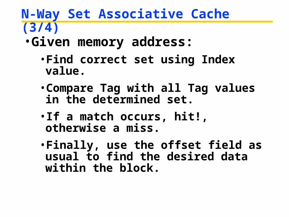
N-Way Set Associative Cache (3/4)•Given memory address:
• Find correct set using Index value.
• Compare Tag with all Tag values in the determined set.
• If a match occurs, hit!, otherwise a miss.
• Finally, use the offset field as usual to find the desired data within the block.

N-Way Set Associative Cache (4/4)•What’s so great about this?
• even a 2-way set assoc cache avoids a lot of conflict misses
• hardware cost isn’t that bad: only need N comparators
• In fact, for a cache with M blocks,• it’s Direct-Mapped if it’s 1-way set assoc
• it’s Fully Assoc if it’s M-way set assoc
• so these two are just special cases of the more general set associative design

Associative Cache Example
• Recall this is how a simple direct mapped cache looked.
• This is also a 1-way set-associative cache!
MemoryMemory Address
0123456789ABCDEF
4 Byte Direct Mapped Cache
Cache Index
0123

Associative Cache Example
• Here’s a simple 2 way set associative cache.
MemoryMemory Address
0123456789ABCDEF
Cache Index
0011

Block Replacement Policy (1/2)•Direct-Mapped Cache: index completely specifies which position a block can go in on a miss
•N-Way Set Assoc: index specifies a set, but block can occupy any position within the set on a miss
•Fully Associative: block can be written into any position
•Question: if we have the choice, where should we write an incoming block?

Block Replacement Policy (2/2)
• If there are any locations with valid bit off (empty), then usually write the new block into the first one.
• If all possible locations already have a valid block, we must pick a replacement policy: rule by which we determine which block gets “cached out” on a miss.

Block Replacement Policy: LRU•LRU (Least Recently Used)
• Idea: cache out block which has been accessed (read or write) least recently
• Pro: temporal locality recent past use implies likely future use: in fact, this is a very effective policy
• Con: with 2-way set assoc, easy to keep track (one LRU bit); with 4-way or greater, requires complicated hardware and much time to keep track of this

Block Replacement Example•We have a 2-way set associative cache
with a four word total capacity and one word blocks. We perform the following word accesses (ignore bytes for this problem):
0, 2, 0, 1, 4, 0, 2, 3, 5, 4
How many hits and how many misses will there be for the LRU block replacement policy?
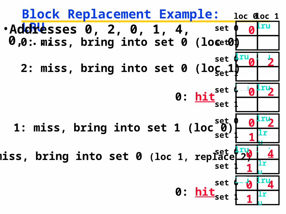
Block Replacement Example: LRU•Addresses 0, 2, 0, 1, 4, 0, ... 0 lru
2
1 lru
loc 0 loc 1
set 0
set 1
0 2lruset 0
set 1
0: miss, bring into set 0 (loc 0)
2: miss, bring into set 0 (loc 1)
0: hit
1: miss, bring into set 1 (loc 0)
4: miss, bring into set 0 (loc 1, replace 2)
0: hit
0set 0
set 1
lrulru
0 2set 0
set 1
lru lru
set 0
set 1
01
lru
lru24lru
set 0
set 1
0 41
lru
lru lru

Big Idea
•How to choose between associativity, block size, replacement policy?
•Design against a performance model• Minimize: Average Memory Access Time
= Hit Time + Miss Penalty x Miss Rate
• influenced by technology & program behavior
• Note: Hit Time encompasses Hit Rate!!!
•Create the illusion of a memory that is large, cheap, and fast - on average

Example
•Assume • Hit Time = 1 cycle
• Miss rate = 5%
• Miss penalty = 20 cycles
• Calculate AMAT…
•Avg mem access time = 1 + 0.05 x 20
= 1 + 1 cycles
= 2 cycles

Ways to reduce miss rate
•Larger cache• limited by cost and technology
• hit time of first level cache < cycle time
•More places in the cache to put each block of memory – associativity
• fully-associative- any block any line
• N-way set associated- N places for each block
- direct map: N=1

Improving Miss Penalty
•When caches first became popular, Miss Penalty ~ 10 processor clock cycles
•Today 2400 MHz Processor (0.4 ns per clock cycle) and 80 ns to go to DRAM 200 processor clock cycles!
Proc $2
DR
AM
$
MEM
Solution: another cache between memory and the processor cache: Second Level (L2) Cache

Analyzing Multi-level cache hierarchy
Proc $2
DR
AM
$
L1 hit time
L1 Miss RateL1 Miss Penalty
Avg Mem Access Time = L1 Hit Time + L1 Miss Rate * L1 Miss Penalty
L1 Miss Penalty = L2 Hit Time + L2 Miss Rate * L2 Miss Penalty
Avg Mem Access Time = L1 Hit Time + L1 Miss Rate * (L2 Hit Time + L2 Miss Rate * L2 Miss Penalty)
L2 hit time L2 Miss Rate
L2 Miss Penalty

Typical Scale
•L1 • size: tens of KB• hit time: complete in one clock cycle
• miss rates: 1-5%
•L2:• size: hundreds of KB• hit time: few clock cycles
• miss rates: 10-20%
•L2 miss rate is fraction of L1 misses that also miss in L2
• why so high?

Example: with L2 cache
•Assume • L1 Hit Time = 1 cycle
• L1 Miss rate = 5%
• L2 Hit Time = 5 cycles
• L2 Miss rate = 15% (% L1 misses that miss)
• L2 Miss Penalty = 200 cycles
•L1 miss penalty = 5 + 0.15 * 200 = 35
•Avg mem access time = 1 + 0.05 x 35= 2.75 cycles

Example: without L2 cache
•Assume • L1 Hit Time = 1 cycle
• L1 Miss rate = 5%
• L1 Miss Penalty = 200 cycles
•Avg mem access time = 1 + 0.05 x 200= 11 cycles
•4x faster with L2 cache! (2.75 vs. 11)

C P U
C a c h e
B u s
M e m o r y
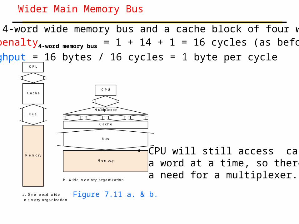
One-Word-Wide Memory Bus
Although caches are interested in low–latency main memory, it is generally easier to improvememory bandwidth with new organization thanit is to reduce latency.
Let us assume the performance of the mainmemory to be:– 1 clock cycle to send address,– 14 clock cycles for the access time per word,– 1 clock cycle to send word of data.
Given a cache block of 1 word (1 word=4 bytes):Miss penalty = 1+14+1 = 16 cyclesThroughput = 4 bytes / 16 cycles = ¼ bytes per cycle
C P U
C a c h e
B u s
M e m o ry
a . O n e - w o rd - w i d e
m e m o ry o r g a n iz a t io n
C P U
B u s
b . W id e m e m o ry o rg a n iz a t io n
M e m o r y
M u lt ip le x o r
C a c h e
Wider Main Memory Bus
• CPU will still access cache a word at a time, so there is a need for a multiplexer.
Given 4-word wide memory bus and a cache block of four words:Miss penalty4-word memory bus = 1 + 14 + 1 = 16 cycles (as before)
Throughput = 16 bytes / 16 cycles = 1 byte per cycle
Figure 7.11 a. & b.

Wider Main Memory Bus & Level 2 Cache
C P U
B u s
M e m o r y
M u l t ip le x o r
C a c h e
– But the multiplexer may be on the critical timing path.– Here, the second level cache can help since multiplexing can be between first- and second-level caches, not on critical timing path.

C P U
C a c h e
B u s
M e m o r y
b a n k 1
M e m o r y
b a n k 2
M e m o r y
b a n k 3
M e m o r y
b a n k 0
Interleaved Memory Organization
The example assumes word addressing. With byte addressing and 4 bytes per word,each of addresses would be multiple of 4.
Memory bus width is 1 word.
Assuming cache block of four words:Miss penalty = 1 + 14 + 4×1 = 19 cycles,Throughput = 16 bytes / 19 cycles = 0.84 bytes per cycle
One address is sent to all banks, and each bank sends its data inits clock cycle.
This is four-way interleaved memory.

What to do on a write hit?•Write-through
• update the word in cache block and corresponding word in memory
•Write-back• update word in cache block• allow memory word to be “stale”
add ‘dirty’ bit to each block indicating that memory needs to be updated when block is replaced
OS flushes cache before I/O…
•Performance trade-offs?

Peer Instructions
1. In the last 10 years, the gap between the access time of DRAMs & the cycle time of processors has decreased. (I.e., is closing)
2. A 2-way set-associative cache can be outperformed by a direct-mapped cache.
3. Larger block size lower miss rate
ABC1: FFF2: FFT3: FTF4: FTT5: TFF6: TFT7: TTF8: TTT

Generalized Caching•We’ve discussed memory caching in detail. Caching in general shows up over and over in computer systems
• Filesystem cache• Web page cache• Game Theory databases / tablebases• Software memoization• Others?
•Big idea: if something is expensive but we want to do it repeatedly, do it once and cache the result.
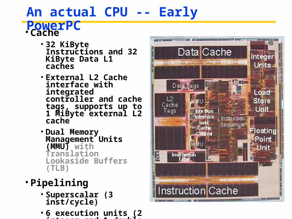
An actual CPU -- Early PowerPC• Cache
• 32 KiByte Instructions and 32 KiByte Data L1 caches
• External L2 Cache interface with integrated controller and cache tags, supports up to 1 MiByte external L2 cache
• Dual Memory Management Units (MMU) with Translation Lookaside Buffers (TLB)
• Pipelining• Superscalar (3
inst/cycle)• 6 execution units (2
integer and 1 double precision IEEE floating point)
Cache Things to Remember• Caches are NOT mandatory:• Processor performs arithmetic, memory stores data• Caches simply make data transfers go faster
• Each Memory Hiererarchy level subset of next higher level
• Caches speed up due to temporal locality: store data used recently
• Block size > 1 wd spatial locality speedup:Store words next to the ones used recently
• Cache design choices:• size of cache: speed v. capacity• direct-mapped v. associative• choice of N for N-way set assoc• block replacement policy• 2nd level cache? 3rd level cache?• Write through v. write back?
• Use performance model to pick between choices, depending on programs, technology, budget, ...