california state university, northridge modeling of
TRANSCRIPT

CALIFORNIA STATE UNIVERSITY, NORTHRIDGE
Modeling of Gallium Nitride MESFETs at High Temperatures
A graduate project submitted in partial fulfillment of the requirements
For the degree of Master of Science in
Electrical Engineering
By
FNU Syed Zabiullah
May 2015

ii
The graduate project of FNU Syed Zabiullah is approved:
Professor Dr. Matthew Radmanesh Date
Professor Dr. Kourosh Sedghisigarchi Date
Professor Dr. Somnath Chattopadhyay, Chair Date
California State University, Northridge

iii
Acknowledgement
I would like to express my sincere gratitude and appreciation to everyone who
made this thesis possible. Most of all, I would like to thank my project coordinator, Dr.
Somnath Chattopadhyay for his guidance in achieving my thesis objective. It was an
honor getting the privilege to work under his supervision. I would also like to thank my
other committee members, Dr. Matthew Radmanesh and Dr. Kourosh Sedghisigarchi for
providing their valuable suggestions.
I would also like to thank the Department of Electrical and Computer Engineering
for providing the facilities to complete this project.
Finally, I would like to express my love and gratitude to my parents; for their
understanding & endless love, through the duration of my studies.

iv
Table of Contents
Signature Page .................................................................................................................... ii
Acknowledgement ............................................................................................................. iii
List of Figures ................................................................................................................... vii
List of Tables ................................................................................................................... viii
ABSTRACT ....................................................................................................................... ix
Chapter 1 Introduction .........................................................................................................1
Chapter 2 Overview of GaN Material ..................................................................................7
2.1 Gallium Nitride properties: ....................................................................................... 7
2.2 Energy- Band Structure............................................................................................. 8
2.2.1 Band structure of Zinc Blend GaN: ................................................................... 8
2.2.2 Band structure of wurtzite GaN: ........................................................................ 9
2.2.3 Temperature dependence of band gap energy: ................................................ 10
2.2.4 Band gap energy Vs Temperature for Wurtzite structure of GaN ................... 10
2.2.5 Band gap energy vs Temperature for Wurtzite GaN: ...................................... 11
2.2.6 Band gap energy vs Temperature for zinc blende GaN on MgO substrate: .... 12
2.2.7 Band gap energy vs temperature of zinc blende GaN with Si substrate: ......... 12
2.3 Intrinsic carrier concentration ................................................................................. 13
2.4 GaN Crystal Structure ............................................................................................. 15
2.5 Various charge effects in GaN: ............................................................................... 18
2.5.1 Piezoelectric effect on GaN: ............................................................................ 18
2.5.2 Polarization charge effect: ............................................................................... 19
2.6 Drift velocity versus electric field: ......................................................................... 21
2.7 Growth process of GaN: ......................................................................................... 22
v
2.8 Why the SiC, Si and sapphire are used for GaN? ................................................... 24
2.9 Growth defects and process induced defects of GaN: ............................................ 25
2.9.1 Native Point Defects: ....................................................................................... 25
2.9.2 Interstitials and Antisites Defects: ................................................................... 26
Chapter 3 Ion Implantation ................................................................................................28
3.1 Ion Implantation ...................................................................................................... 28
3.1.1 Ion implantation equipment: ............................................................................ 30
3.2 Impurity distribution equation: ............................................................................... 31
3.3 Annealing: ............................................................................................................... 34
3.4 Fabrication process of MESFET:............................................................................ 35
Chapter 4 Physics of MESFET ..........................................................................................38
4.1 MESFET: ................................................................................................................ 38
4.2 Working of MESFET:............................................................................................. 39
4.2.1 Types of MESFETS and its operations:........................................................... 39
4.3 MESFET Characteristics: ....................................................................................... 41
4.3.1 I-V Characterisctics: ........................................................................................ 41
4.3.2 Operating Regions in MESFET: ...................................................................... 42
4.4 MESFET applications in various fields: ................................................................. 43
Chapter 5 Theory and Calculations....................................................................................45
5.1 I-V characteristics Of GaN MESFET: .................................................................... 45
5.2 Trans-conductance of GaN MESFET: .................................................................... 46
5.3 Temperature dependence of GaN properties: ......................................................... 47
Chapter 6 Results and Discussion ......................................................................................48
6.1 Temperature versus current: ................................................................................... 48
6.2 I-V characteristics: .................................................................................................. 49

vi
6.3 I-V characteristics for different active channel thickness (a): ................................ 50
6.4 Transconductance by varying temperature: ............................................................ 51
Chapter 7 Conclusion .........................................................................................................53
References ..........................................................................................................................54
APPENDIX A ....................................................................................................................66
APPENDIX B ....................................................................................................................68

vii
List of Figures
Figure 2.1 Energy band diagram for Zinc Blend GaN........................................................ 8
Figure 2.2 Energy band diagram of wurtzite GaN .............................................................. 9
Figure 2.3 Excitation energies vs Temperature plot ......................................................... 11
Figure 2.4 Band gap (eV) vs Temperature (K) plot .......................................................... 11
Figure 2.5 Temperature (T) vs Band gap (eV) plot .......................................................... 12
Figure 2.6 Band energy vs Temperature plot for zinc blende GaN with Si as substrate .. 13
Figure 2.7 Intrinsic carrier concentration vs Temperature ................................................ 15
Figure 2.8 The correlation between lattice constant of zinc blende and wurtzite and band
energy gap for various materials and their related alloys ................................................. 16
Figure 2.9 Structures of atoms for zinc blend (a), wurtzite (b), rocksalt (c) .................... 17
Figure 2.10 Drift velocity vs electric field for GaN.......................................................... 22
Figure 2.11 Principle of MOVCD process ....................................................................... 23
Figure 2.12 Formations of Energies at Fermi Level for Native Point Defects ................. 26
Figure 3.1 (a) Doping by diffusion, (b) Doping by ion implantation ............................... 29
Figure 3.2 Schematic of medium current ion implanter ................................................... 30
Figure 3.3 Schematic for the ion range ............................................................................. 33
Figure 3.4 Boron implanted atom distribution .................................................................. 34
Figure 3.7 Steps involving MESFET fabrication ............................................................. 37
Figure 4.1: Schematic representation of Gallium Nitride MESFET................................. 38
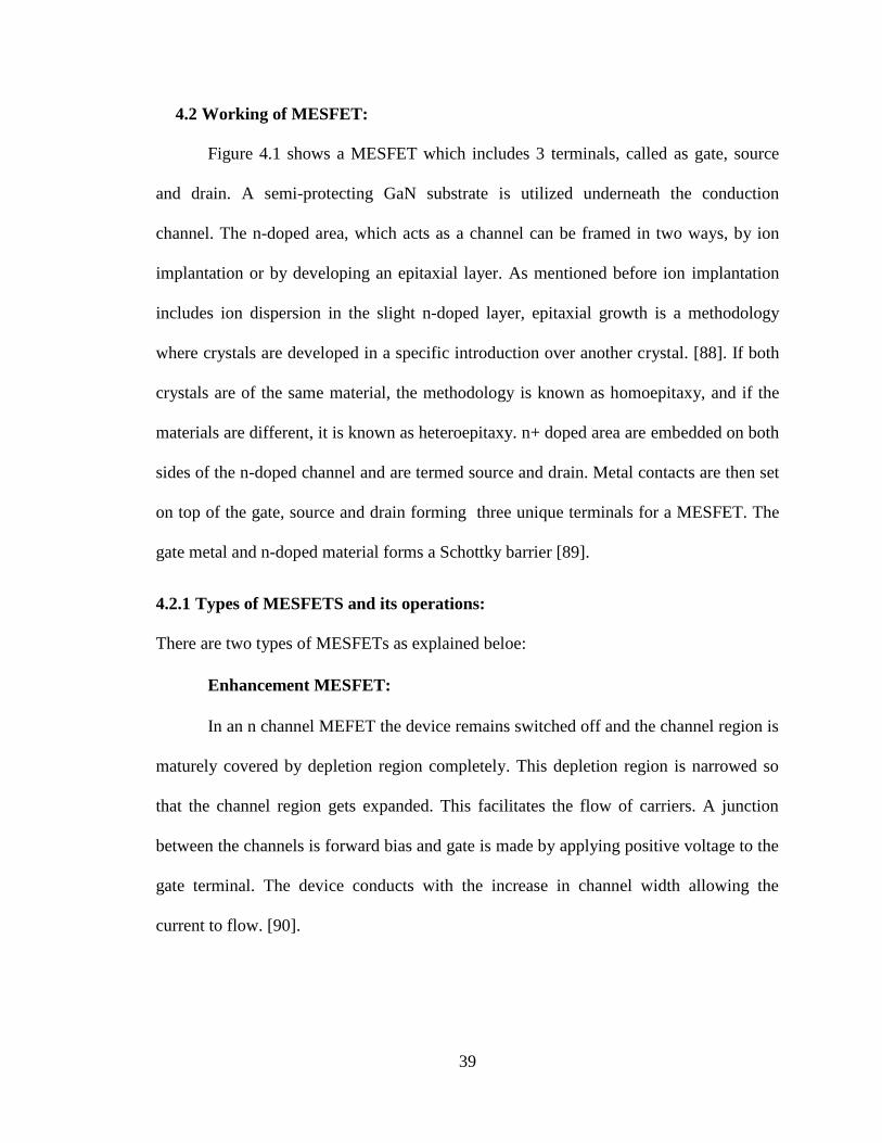
Figure 4.2: E-MESFET ..................................................................................................... 40
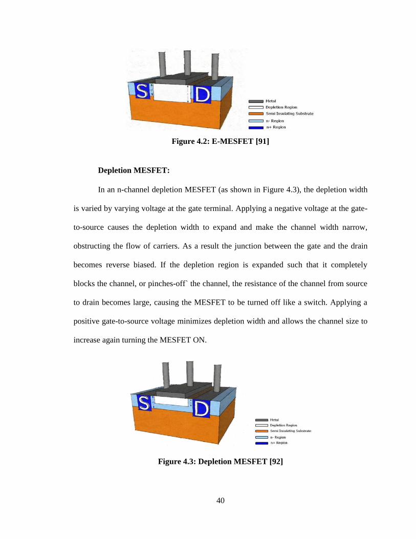
Figure 4.3: Depletion MESFET ........................................................................................ 40
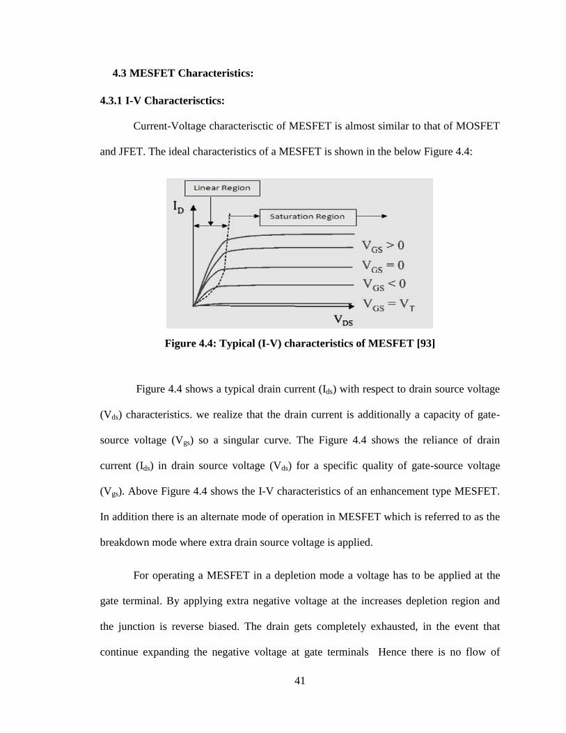
Figure 4.4: Typical (I-V) characteristics of MESFET ...................................................... 41
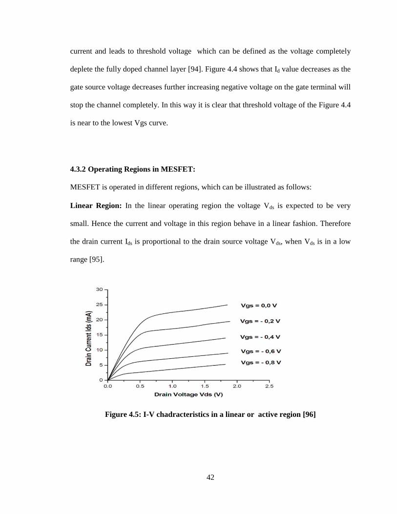
Figure 4.5: I-V chadracteristics in a linear or active region ............................................ 42
Figure 4.6: Drain-source current vs drain-source voltage in saturation region ................ 43
Figure 5.1: Gallium Nitride MESFET shown in a cross-sectional view .......................... 45
Figure 6.1 Variation of current with change in temperature ............................................. 48
Figure 6.2: Ids versus Vds plot by giving different gate source voltage Vgs ...................... 49
Figure 6.3: Ids versus Vds plot for different active channel thickness. .............................. 50
Figure 6.4 Variation of Transconductance with Temperature: ......................................... 51
viii
List of Tables
Table 1.1 Physical properties of various semiconductor materials ..................................... 2
Table 2.1 Properties of various materials ........................................................................... 7
Table 2.2: Lattice constants and unit cell parameters for GaN, AIN, InN ....................... 18
Table 5.1: GaN parameters at different temperature: ....................................................... 47
ix
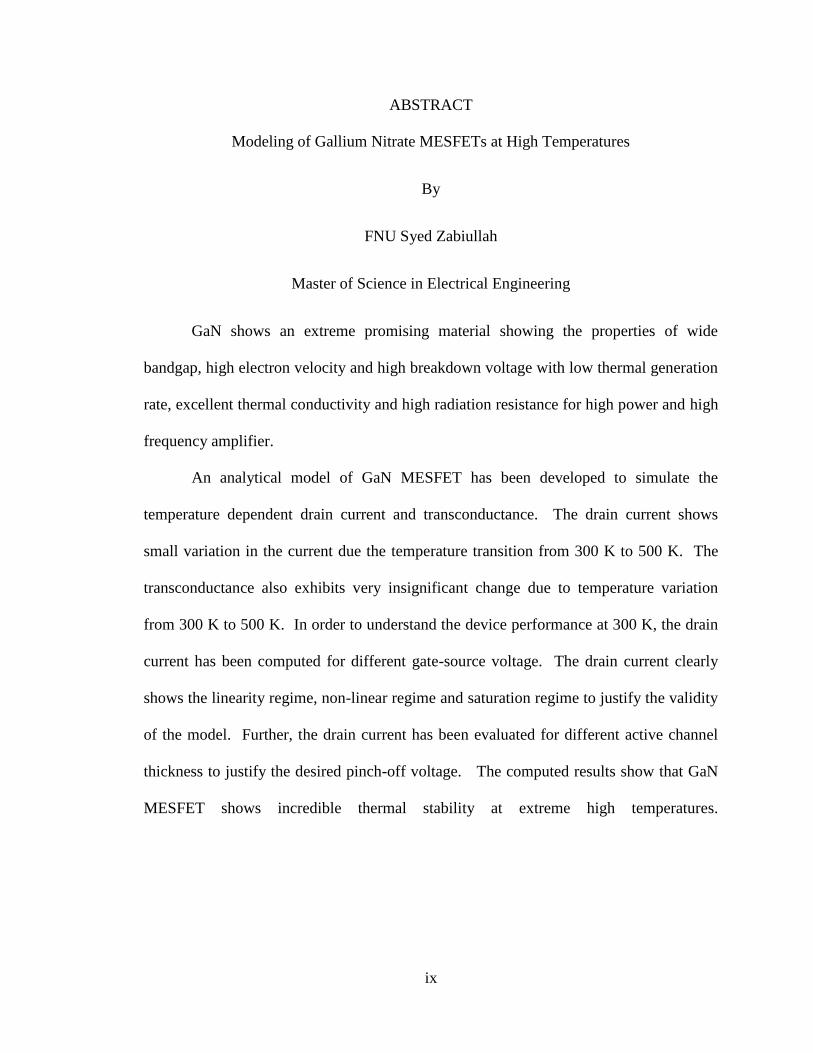
ABSTRACT
Modeling of Gallium Nitrate MESFETs at High Temperatures
By
FNU Syed Zabiullah
Master of Science in Electrical Engineering
GaN shows an extreme promising material showing the properties of wide
bandgap, high electron velocity and high breakdown voltage with low thermal generation
rate, excellent thermal conductivity and high radiation resistance for high power and high
frequency amplifier.
An analytical model of GaN MESFET has been developed to simulate the
temperature dependent drain current and transconductance. The drain current shows
small variation in the current due the temperature transition from 300 K to 500 K. The
transconductance also exhibits very insignificant change due to temperature variation
from 300 K to 500 K. In order to understand the device performance at 300 K, the drain
current has been computed for different gate-source voltage. The drain current clearly
shows the linearity regime, non-linear regime and saturation regime to justify the validity
of the model. Further, the drain current has been evaluated for different active channel
thickness to justify the desired pinch-off voltage. The computed results show that GaN
MESFET shows incredible thermal stability at extreme high temperatures.

1
Chapter 1 Introduction
In recent years a greater interest has been paid to the wide band-gap materials
such as Gallium Nitride (GaN) [1] due to its low thermal generation rate and high
breakdown field as it has a potential in high power [2], high temperature and microwave
frequency application. GaN is being used in high frequency electronic devices and these
devices are commercialized. Because of gallium nitride’s incredible properties, wide
band gap which cause high electric field breakdown gives GaN potential in high power
device area and are used for military purposes [3-4].
The wide band gap materials such as GaN, SiC typically has an order of
magnitude greater when compared to the other conventional semiconductors [5]. The
band gap energies of these materials are multiple times greater than that of conventional
semiconductors namely Si, GaAs, InP. The wide band-gap materials can be operated at
high voltage supply because of high breakdown field (Ec) which is due to their wide band
gap (Eg). GaN material has an ability to withstand at high operating temperatures and
accepts improved radiation hardness. High thermal conductivity of GaN plays an
important role because most of the electronic devices are projected for high power
applications and the ability to extract heat caused due to dissipated energy results the
better performance of the device [6]. Silicon and Gallium Nitride has almost similar
thermal conductivity but the thermal conductivity of SiC is multiple times higher than
that of GaN and Si. The thermal conductivity of Gallium Nitride was calculated to be 130
W/mK [7].
Wide band-gap materials are capable of making lesser noise than conventional
semiconductors and thus GaN is encouraged in ultra-violet range in producing high
2
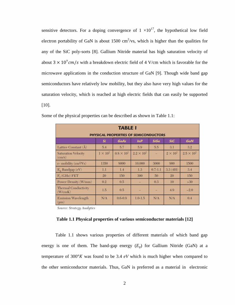
sensitive detectors. For a doping convergence of 1 ×10¹⁷
, the hypothetical low field
electron portability of GaN is about 1500 cm2/vs, which is higher than the qualities for
any of the SiC poly-sorts [8]. Gallium Nitride material has high saturation velocity of
about with a breakdown electric field of 4 V/cm which is favorable for the
microwave applications in the conduction structure of GaN [9]. Though wide band gap
semiconductors have relatively low mobility, but they also have very high values for the
saturation velocity, which is reached at high electric fields that can easily be supported
[10].
Some of the physical properties can be described as shown in Table 1.1:
Table 1.1 Physical properties of various semiconductor materials [12]
Table 1.1 shows various properties of different materials of which band gap
energy is one of them. The band-gap energy (Eg) for Gallium Nitride (GaN) at a
temperature of 300 was found to be 3.4 eV which is much higher when compared to
the other semiconductor materials. Thus, GaN is preferred as a material in electronic
3
devices [13].
The performance of high power and high frequency devices totally depend on the
material characteristics such as conduction efficiency, switching speed, cost, size of
material and breakdown voltage. These characteristics determine the power density and
frequency of the device [14]. Gallium Nitride (GaN) has indicated great attributes
towards electronic and optical devices at high temperatures, high frequencies and high
power. By using GaN material many different varieties of electronic devices have been
modeled which offers high performance in microwave frequencies when compared to Si
and GaAs devices [15].
Gallium Nitride (GaN) metal semiconductors field effect transistors (MESFET)
was developed first in the year 1993 and from then various researches has been carried
out. GaN MESFETs were developed to substitute power MOSFETs in applications where
power conversion efficiency and switching speeds are important [16]. GaN MESFET has
its applications in various aspects such as military, aerospace, Radars etc. GaN MESFETs
are receiving more awareness as it has a structure which is simple to analyze when
compared to other complicated transistors such as high electron mobility transistors
(HEMT) [17].
Analytical modeling has been conducted on GaN MESFETs various times,
though significant experimental work is available [18]. In recent researches it has been
reported GaN MESFET is encouraging in power performance. In a research, the current
device performance exhibited a power density of 2.2 W/mm with a power added
efficiency of 27% at VDS = 30V and VGS = 2V at 2GHz [19]. In some other research
conducted on the GaN based MESFET, device showed a high frequency of 10 GHz with
4
power density of 2.7 W/mm [20]. In a research conducted on GaN MESFET based device
a cut-off frequency of 900 MHz and an output power of 51 W with 78 % power added
efficiency was shown [21]. In another GaN MESFET device 10W output power with a
power added efficiency (PAE) of 34% at = 48V and a cut off frequency of 700 MHz
and maximum frequency of 1.8 GHz was achieved [22]. A 0.8µm x 150µm GaN
MESFET has been reported with a cut off frequency of 6.5 GHz and a maximum
frequency of 14GHz. These are in lateral agreement with their measured values
of 6 and 14 GHz using a technique called Volterra-series technique [23], where the 1-dB
compression point and output-referred third-order intercept points are 16.3dBm and
22.2dBm, respectively. In this case a constant channel temperature of 300K is assumed
whereas some other researchers have achieved cut off frequency ) of 20 GHz and a
maximum frequency of 50 GHz [24]. Hence the above measurements show the
high frequency performance of GaN material which was discussed at the beginning.
In a research, GaN MESFET based device showed a performance of 2GHz cutoff
frequency with power density of 2.2 W/mm and had an associated power added
efficiency of 27% at [25]. In another research, the threshold
voltage for a GaN MESFET was found to be in a range of 4 V to 20 V with maximum
drain current which went up to 300 mA/mm and transconductance values of up to 60
mS/mm. This was measured for a device with 100 µm gate length which created potential
performance for high frequency applications [26].
In a research conducted on a DC and microwave performances of GaN MESFET
using ICP-RIE, a small signal RF performance was measured using a network analyzer
from 1GHz to 35 GHz at VDS =20 v and VGS=-0.5 v. The cut-off frequency was measured

5
as 28 GHz and the maximum frequency was measured as 55 GHz [27].
For a non-surface-depleted GaN MESFET, it has been found that the maximum
trans-conductance ) was 244 mS/mm and the maximum cut-off frequency 230 GHz,
with a maximum output power of 2.66 W/mm [28]. In a GaN based MESFET device
research, cutoff frequency ( was measured to be 6.35 GHz and maximum frequency
( was found to be 10.25 GHz in a 0.1 µm gate-length zinc blende crystal structure
[29]. In this case GaN MESFET showed a maximum cut-off frequency of 220 GHz and
trans-conductance of 210 mS/mm [30].
In a GaN MESFET research the output power of 230W and a cut-off frequency
( ) of 30 GHz for a gate length of 0.25 µm was found [31]. With a drain current of 500
mA at = 40 V and = 0 V GaN MESFET device was fabricated and this device
resulted in a cut-off frequency of 8 GHz, trans-conductance ) of 93mS/mm and an
output power of 4W/mm with a power added efficiency of 50% and a gain 20dBm. These
results were better than SiC MESFET simulation by the same researcher [32]. During
another research a GaN MESFET device was fabricated with = 15.6 GHz and =
7.2 GHz, transconductance of 164 mS/mm with a PAE of 38% at = 3.5V [33].
Gallium Nitride (GaN) has been fabricated on HEMTs. A research was conducted
for a Sapphire GaN/AlGaN based HEMT devices which had a 1 nm aluminum nitride
(AlN) interlayer at a room temperature and a mobility of 1780 . An electron sheet
carrier density of which exhibited a power density of 4.9 W/mm, a
linear gain of 14 dB and a PAE beyond 32 % are obtained at 10 GHz with a gate width of
1 mm were accomplished [34]. A research on GaN HEMT device with Silicon Carbide
(SiC) as a substrate, a maximum power added efficiency greater than 56% while
6
maintaining output power of 205 Watts with a cutoff frequency of 1.2 GHz and
maximum frequency of 1.4 GHz was found[35]. A research was carried out on a AlGaN
mole fraction HEMT structure on Semi-insulating SiC substrates. This resulted in an
output power of 103 W with a high power density of 5.2 W/mm and power added
efficiency (PAE) of 35.3% [36]. A research on AlGaN/GaN power HEMT in sapphire
substrate showed an output power density of 1.1W/mm with PAE of 20.1%. A cutoff
frequency ( ) of 36 GHz and maximum frequency ( ) of 70 GHz was achieved. In
this case, gate-to-drain breakdown voltage up to 230V and channel current greater than
300 was obtained [37]. Some researchers have obtained the transconductance of
68mS/mm with maximum frequency of approximately 31 GHz and a cutoff frequency of
1.8 GHz with an RF power of 84 mW/mm. In this case maximum drain to source current
density was approximately 174 mA/mm for a 1400 mm wide gate AlGaN/GaN HEMT
with = -1.1V and = 6V [38-39].
7
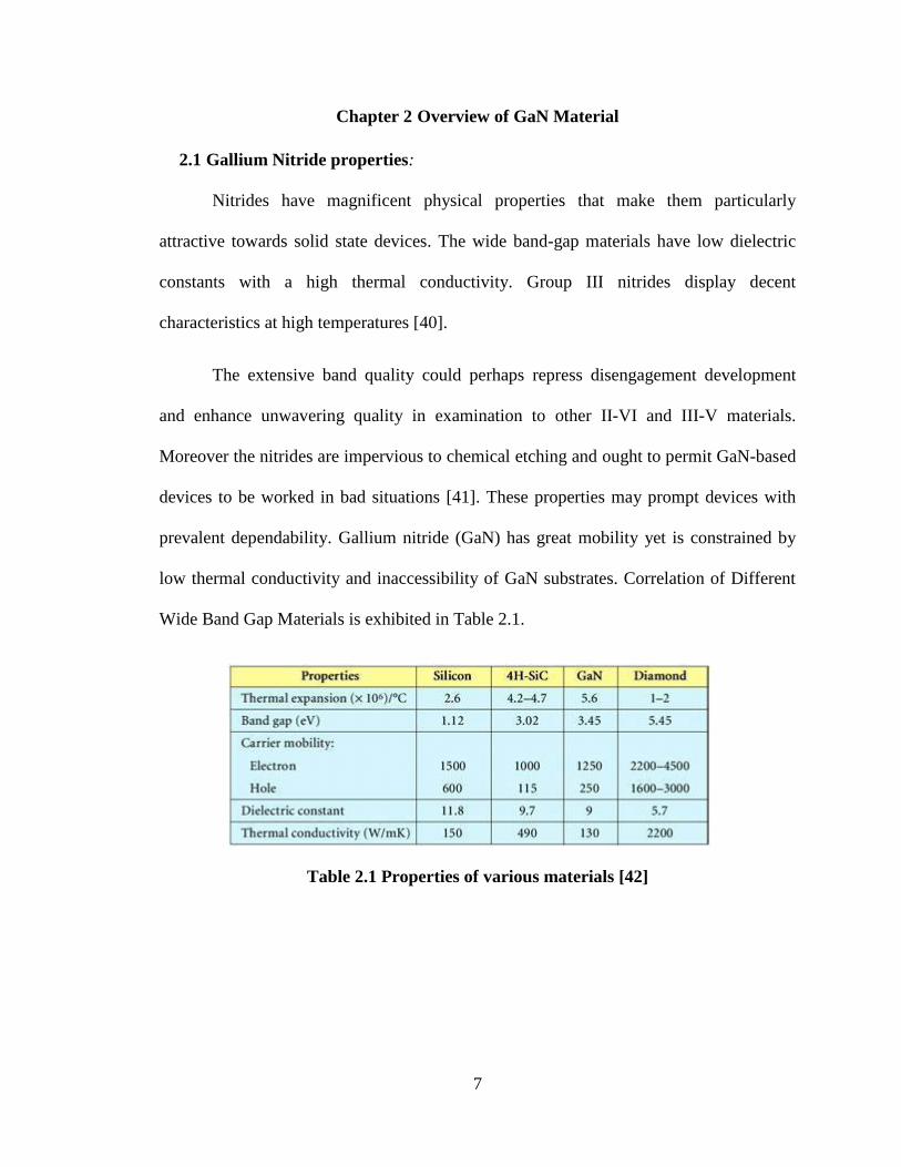
Chapter 2 Overview of GaN Material
2.1 Gallium Nitride properties:
Nitrides have magnificent physical properties that make them particularly
attractive towards solid state devices. The wide band-gap materials have low dielectric
constants with a high thermal conductivity. Group III nitrides display decent
characteristics at high temperatures [40].
The extensive band quality could perhaps repress disengagement development
and enhance unwavering quality in examination to other II-VI and III-V materials.
Moreover the nitrides are impervious to chemical etching and ought to permit GaN-based
devices to be worked in bad situations [41]. These properties may prompt devices with
prevalent dependability. Gallium nitride (GaN) has great mobility yet is constrained by
low thermal conductivity and inaccessibility of GaN substrates. Correlation of Different
Wide Band Gap Materials is exhibited in Table 2.1.
Table 2.1 Properties of various materials [42]

8
2.2 Energy- Band Structure
2.2.1 Band structure of Zinc Blend GaN:
Figure 2.1 Energy band diagram for Zinc Blend GaN [43]
Figure 2.1 depicts the energy band diagram for gallium nitride with zinc blend as
crystal. Energy band gap (Eg) in the band structure shows that it has a value of 3.2 eV in
the -valley is measured through the conduction band minima and valence band maxima
at k (wave vector) = 0. The energy band gap in X-valley is defined as Ex and has a value
of 4.6 eV. L-valley has a band gap designated as EL comprising a value of 4.8 to 5.1 eV.
The value of Es0 is 0.02 eV and is called split-off band in the valence band.

9
2.2.2 Band structure of wurtzite GaN:
Figure 2.2 Energy band diagram of wurtzite GaN [44]
Above Figure 2.2 depicts the energy band diagram for gallium nitride with zinc
blend as crystal. The energy band-gap (Eg) with a value of 3.39 eV in the -valley is
measured through the conduction band minima and valence band maxima at k (wave
vector) = 0. The energy band gap in A-valley is defined as EA and has a value of 4.7-5.5
eV. L-valley has a band gap designated as EM-L comprising a value of 4.5 to 5.13 eV. The
value of Es0 0.08 eV and is called split-off band in the valence band.

10
2.2.3 Temperature dependence of band gap energy:
The temperature dependent energy band gap can be calculated with the help of
following equation [45],
(2.1)
Where, Eg is energy band gap at temperature T (in degrees kelvin) and Eg (0) is band gap
energy at K and has a value of 3.47 eV for wurtzite crystal and a value of 3.28 eV for
zinc blende GaN.
Temperature dependence energy band gap can also be calculated with the help of
Varshni expression [46] is given by,
(2.2)
Where, the value of energy band gap at 0 K is given as 3.427 eV.
2.2.4 Band gap energy Vs Temperature for Wurtzite structure of GaN
From above we know that the energy band gap of wurtzite GaN at 0 is 3.47
eV. Energy band gap for the temperatures below 295 K is expressed by the equation [47],
(2.3)
Where T is in kelvin and the value of band gap energy Eg, at 300K is calculated
to be 3.44 eV and Eg (T) temperature dependent excitation energy band gap. This can be
represented graphically in a Figure 2.3 as shown below.

11
Figure 2.3 Excitation energies vs Temperature plot [48]
Figure 2.3 plot shows that the temperature is low at high excitation energy. As the
temperature increases, the value of excitation energy decreases exponentially. It
decreases from 3.505 eV to 3.44 eV when temperature increases from 0 to 300K.
2.2.5 Band gap energy vs Temperature for Wurtzite GaN:
Figure 2.4 Band gap (eV) vs Temperature (K) plot [49]

12
Gallium Nitride samples by using different techniques were grown on different
substrates such as SiC, Si and sapphire [50]. From the Figure 2.4, it shows that band gap
energy for wurtzite GaN gradually decreases as the temperature is increased, which
means that band gap energy is inversely proportional to the temperature.
2.2.6 Band gap energy vs Temperature for zinc blende GaN on MgO substrate:
Zinc blende GaN film was grown on the magnesium oxide (MgO) substrate.
When the temperature of the substrate was increases the energy band gap decreases from
3.3 eV to 3.23 eV for a temperature range of 0 to 300K. This can be presented in the
Figure 2.5 below.
Figure 2.5 Temperature (T) vs Band gap (eV) plot [51]
2.2.7 Band gap energy vs temperature of zinc blende GaN with Si substrate:
When a zinc blende GaN films was grown on silicon (100) substrates, the dependencies
were extracted by using two different theoretical models from pseudo electric function.

13
Figure 2.6 Band energy vs Temperature plot for zinc blende GaN with Si as
substrate [52]
In the above Figure 2.6, the band gap energy is decreased with increase of the
temperature when GaN growth was made on the Si substrate.
2.3 Intrinsic carrier concentration
Intrinsic carrier concentration is the concentration of free carriers which are
created in the valence and conduction bands because of the thermal excitation of the
carriers in both conduction and valence band. It is designated as ni or Ni. It is defined as
the equal number of electrons in the conduction band and equal number of holes in the
valence band in intrinsic material [53]. Higher band gap materials have lower intrinsic
carrier concentration because the thermal excitation of carriers is difficult for the higher
band gap material such as GaN. Intrinsic carrier concentration plays an important role in

14
inheriting quality of GaN as wide band gap properties. Intrinsic carrier concentration can
be calculated with the help of following equation [54],
(2.4)
Where, Nc and Nv are effective density of states in conduction and valence band
respective, Eg is the band gap energy, T is the temperature in Kelvin and KB is Boltzmann
constant having a value constant value
The effective density of states in the conduction band (Nc) which can be expressed as,
For Zinc blende structure (
)
(2.5)
For Wurtzite structure (
)
(2.6)
is the effective density of states in the Valance band which can be valued by
below equation:
For Zinc blende structure
(2.7)
For Wurtzite structure
(2.8)
“Intrinsic carrier concentration depends on the temperature and can be evaluated
from the following plot.”

15
Figure 2.7 Intrinsic carrier concentration vs Temperature [55]
Figure 2.7 shows that the intrinsic concentration for both zinc blende and
wurtzite GaN reaches to the value of 10-9
cm-3
at room temperature and the intrinsic
carrier concentration linearly increases with high temperature. The intrinsic carrier
concentration of GaN at 850ok is approximately 10
10cm
-3, which is almost the same as
silicon at 300 K. Hence, the property of intrinsic carrier concentration shows that the
GaN is having more withstanding potentiality in high temperature environment compared
to silicon and GaAs [56]. Zinc Blende GaN structure has higher intrinsic carrier
concentration when compared to the wurtzite GaN.
2.4 GaN Crystal Structure
Generally Gallium Nitride (GaN) is crystalized by either zinc blende crystal or by
wurtzite structure. The modifications of GaN, AIN, InN by zinc blende or wurtzite are
identical but has some kind of significant differences [57].
16
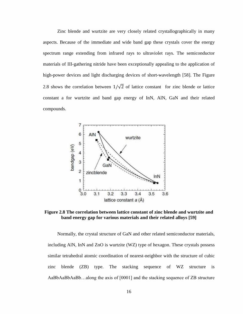
Zinc blende and wurtzite are very closely related crystallographically in many
aspects. Because of the immediate and wide band gap these crystals cover the energy
spectrum range extending from infrared rays to ultraviolet rays. The semiconductor
materials of III-gathering nitride have been exceptionally appealing to the application of
high-power devices and light discharging devices of short-wavelength [58]. The Figure
2.8 shows the correlation between √ of lattice constant for zinc blende or lattice
constant a for wurtzite and band gap energy of InN, AlN, GaN and their related
compounds.
Figure 2.8 The correlation between lattice constant of zinc blende and wurtzite and
band energy gap for various materials and their related alloys [59]
Normally, the crystal structure of GaN and other related semiconductor materials,
including AlN, InN and ZnO is wurtzite (WZ) type of hexagon. These crystals possess
similar tetrahedral atomic coordination of nearest-neighbor with the structure of cubic
zinc blende (ZB) type. The stacking sequence of WZ structure is
AaBbAaBbAaBb…along the axis of [0001] and the stacking sequence of ZB structure

17
is AaBbCcAaBbCc…along the axis of [111], where Aa, Bb, Cc represent the three
types of cation and anion location in the lattice of triangle on the planes of (0001) and
(111). This is are demonstrated by Figure 2.9.
Figure 2.9 Structures of atoms for zinc blend (a), wurtzite (b), rocksalt (c) [60]
If stacking sequence is the factor which discriminates the structure of zinc blende
and the wurtzite then, c/a=1.633 will exist between wurtzite structure lattice constants.

18
The crystal lattice parameters of various materials can be shown in the table
below,
Table 2.2: Lattice constants and unit cell parameters for GaN, AIN, InN [61]
2.5 Various charge effects in GaN:
2.5.1 Piezoelectric effect on GaN:
Piezoelectric is created by combining epitaxial growth which is performed in the c
plane [0001] orientation of wurtzite crystal structure of GaN. The associated electrostatic
charge densities had influenced many properties namely electric field, carrier distribution
and some of the optical and electric properties of nitride materials and their devices [62].
Some results of positional dependence of the piezoelectric polarization, piezoelectric
charge distribution and conduction band potential profile for several possible
approximations are determined. In GaN quantum well (QW) hetero structures are
strongly affected by structural imperfections.
19
2.5.2 Polarization charge effect:
Gallium Nitride materials generally exist in the wurtzite phase because of
which it has strong polarization properties in C-direction. The ball and stick model of
GaN in the basal plane and the associated polarization in the crystal and these
polarizations charges occur on each unit cell when it is in a classical mode. The
summation of internal polarization is null in the crystal after leaving a charge of ± at
each end of the crystal forms a dipole [63]. The screening dipole which is the result of
placing equal and opposite charges at or close to the charges of polarization dipole is
created because of the unscreened dipole, which creates a non-sustainable dipole
moment.
In Gallium Nitride (GaN) the polarization charge density ( ) leads
to an electric field , which is expressed by the following equation [64],
=
1.6 MV/cm (2.9)
Where,
is the polarization charge density,
is the electric field,
is charge
This dipole charge results in a voltage across the material in a crystal of thickness
d = 1 , and this voltage is given by the equation [65],
= .d=160V (2.10)
Where,
is the voltage,
20
is the electric field,
d is the thickness of crystal
This brings up the issue how the charges that form a screening dipole. They could
emerge from counter particles which is present in the atmosphere. This is most likely the
case for mass polar materials utilized as a part of ceramic industry [66]. This is not likely
the situation for epitaxial GaN thin films, since these films can be made in an
environment free of counter particles, for example in a MBE reactor. This creates inquiry
of whether screening of counter particles is conceivable without outside counter particles.
The accompanying examination addresses this issue [67].
Considering, a lightly doped n-type GaN sample in the initial stages of growth.
GaN is hetero-epitaxially grown on sapphire, Si or SiC substrates rather the GaN
substrate due to its lack in availability. The material at the substrate and thin film
interface is highly defective and therefore capable of trapping mobile charges. The effect
of the background n-type doping on the electric field profile within the material is
assumed to be negligible when compared to the electric field generated by the
polarization charges [68]. The effects of surface states on the electrical properties of the
material can be ignored. Both of these effects will be considered later.
In the absence of surface states, as the material becomes thicker the electric field
in the material (given by the slope of the conduction and valence band) will remain
constant until the valence band crosses the Fermi level. The thickness of the film ( at
which this occurs is given by [69].
(2.11)
21
Where, = 3.4 eV is the bandgap of GaN. Once d > , holes begin to
accumulate at the surface (created by generating across the gap), leading to an equal
electron concentration which drifts to the substrate-epi interface (the GaN N-face),
creating a screening dipole. The magnitude of the screening charge increases
continuously with epitaxial layer thickness. The evolution of the screening charge with
distance is obtained by recognizing that the maximum voltage across the structure is the
band gap of the material [70],
| | (
) d (2.12)
=
(2.13)
As d , , or in other words for very thick samples the polarization
dipole is fully screened.
2.6 Drift velocity versus electric field:
Drift velocity in semiconductors is the velocity of the charge carriers under the
influence of electric field. In Figure 2.10 we can see the relationship between the drift
velocity and the electric field for zinc blende and wurtzite gallium Nitride structures.

22
Figure 2.10 Drift velocity vs electric field for GaN [71]
In the Figure 2.10, curve 1 shows how the drift velocity changes when the electric
field is applied for wurtzite structure which is applied in the direction (1010). Drift
velocity increases till certain point and the gradually decreases from 220 kV/cm for
wurtzite structure. Curve 2 shows how drift velocity behaves by increasing the electric
field along (100) direction in the zinc blende structure. Drift velocity increases when
electric field is increased and goes up to 2.6x10⁷cms
-1 for 200 kV/cm of electric field and
then further increase in electric field decreases drift velocity gradually.
2.7 Growth process of GaN:
The hetero structures of GaN and AlGaN/GaN have epitaxially been grown on
different substrates like sapphire, spinel, 6H-SiC, 2H-SiC, Si, and recently on a bulk AlN
and GaN [72]. The Metal- Organic Vapor Phase Epitaxy is a typical technique of GaN
growth. The epitaxial layers are deposited using low pressure MOCVD over basal plane
sapphire substrates in most GaN based devices. Triethylgalium, triethylaluminum and
ammonia as the precursors for ‘Ga’, ‘Al’ and ‘N’ are used for a typical MOCVD growth.

23
The APA Optics group reports a typical growth pressure and temperature of 76 torr and
1000 oC. The two metal organics have a typical flow in the range of 1 to 10 and 1.5 to 0.6
moles/min, respectively. The deposited GaN layers are highly resistive with a carrier
density well below 1015
cm-3
. Using silicon (Si) as the dopant, the insulating GaN layers
can be doped n-type. The quality of the epitaxial GaN depends on the quality of the
substrates and this is shown by the studies of transport properties. All this implies a
considerable interest in the development of bulk GaN crystals for homo epitaxy. In
Warsaw, (Poland) under the direction of Professor Sylvester Porowski, a pioneering
effort in high-pressure bulk growth of GaN is underway. A square centimeter or little
more is typical crystal size. These epitaxial layers have no interface detected and with the
dislocation density below the detection limit and making them an excellent quality.
Figure 2.11 shows the principle involved in MOCVD-process.
Figure 2.11 Principle of MOVCD process [73]
Lateral Epitaxial Overgrowth (LEO) is recently gaining high attention. This
allows production of GaN films with the density of up to 4 orders of magnitude smaller
than for GaN films grown on sapphire and 6H-SiC substrates. The studies of threading

24
dislocations in GaN films have been investigated in the LEO-grown GaN films. There is
a dramatic drop in the leakage current in GaN-based p-n junctions and GaN/AlGaN
hetero-junction field-effect transistors grown by LEO as a result of the dislocation
density. Molecular Beam Epitaxy (MBE) is one other technique of the epitaxial growth of
GaN. GaN layers grown by MBE are similar in quality to the layers grown by MOCVD
[74]. Thick layers of GaN are important for potential applications of GaN-based materials
in power devices and are yielded by HVPE. HVPE technique was used recently for the
epitaxial growth of AlN/AlGaN/GaN hetero structures on SiC substrates. The fabrication
of quantum dots is one interesting emerging direction in the epitaxial growth of GaN,
AlN, and InN materials. Having electron density higher than 1019
cm-3
, 54 N-type GaN
can be obtained. The highest reported hole concentration in p-GaN was around 1018
cm-3
(using Mg as an acceptor) causing p-doping to remain a serious problem. The ionization
energy of this acceptor is quite high (160 meV) so that less than 1% of Mg acceptor is
activated at room temperature is the reason for this behavior [75].
2.8 Why SiC, Si and sapphire are used for GaN?
Gallium Nitride can be manufactured on lot of substrates such as Si, SiC, AIN,
MgO and various others. Before choosing a substrate there are a lot of criteria to go
through such as lattice coincidence, lattice matching, thermal expansion coefficient
(TEC), surface chemistry, temperature stability, conductivity, cleavability, availability,
price. The first MBE developed GaN LED on Si in 1998 which showed that silicon can
be considered as a substrate material for GaN development. A seed layer or buffer layer
to accommodate the lattice mismatch between the substrate and the epi-layer is used for
the GaN growth on sapphire, SiC or Si. The 6H–SiC, 4H–SiC and 3C–SiC substrates for

25
GaN growth has the effect of surface pre-treatment by exposure. This work proposed a
possibility that p-type doping was achievable in GaN on Si and mechanisms could be
found out. In recent years researches have been carried out around there and even from an
optimistic GaN layers on Si are very nearly similar to GaN layers on SiC.
The deposited GaN film was found to be polycrystalline, after the nitration of
Silicon carbide. The development of the seed layer will bring about non-stoichiometric
synthesis at flat temperatures and additionally processes a heightened thickness of defects
in the structure, along these variations. This also brings down the restraint between
Silicon/AlN interfaces. The least resistance utilizing a flat level temperature has been
indicated in LEDs of GaN on Silicon [76].
2.9 Growth defects and process induced defects of GaN:
There could be many defects associated to GaN grown in different substrate.
Most common defects are mismatch of lattice constant, thermal expansion coefficient and
dislocation. There are many other defects such as inversion domain, stacking mismatch
boundaries, micro pipes or nanopipes or voids and surface pits. These defects will cause
the periodicity of the crystal to be dislocated over distances of several atomic diameters.
This will affect the electronic and optoelectronic properties of the device. Dislocation
defects cause rapid recombination of holes with electrons without conversion of their
available energy into photons. This causes heating up of the crystal and making electronic
and optoelectronic devices malfunction [77].
2.9.1 Native Point Defects:
The native defects inside the materials will affect the optical properties and

26
electrical properties of these materials. These defects also cause annealing in the
materials. Vacancies, interstitials, and anti-sites are the different forms these defects can
take. The interaction of isolated native defects causes the formation of complex defects.
Figure 2.12 shows the energy formation at the different levels of the formation energy
(eV).
Figure 2.12 Formations of Energies at Fermi Level for Native Point Defects [78]
2.9.2 Interstitials and Antisites Defects:
The minor cross section consistent in GaN and the expansive size between Ga and
N molecules cause imperfections regularly. Under certain conditions some of the
imperfections might shape yet in extremely little focuses on the other hand. Development
of energies of the Ga interstitial (GaI) and huge cross section relaxations are expedited by
the imposing size of the Ga particles. Large portability of GaN even at room temperature

27
intimates that GaN is trapped by some different deformities and does not exist in GaN as
a confined negative aspect in equilibrium.
28
Chapter 3 Ion Implantation
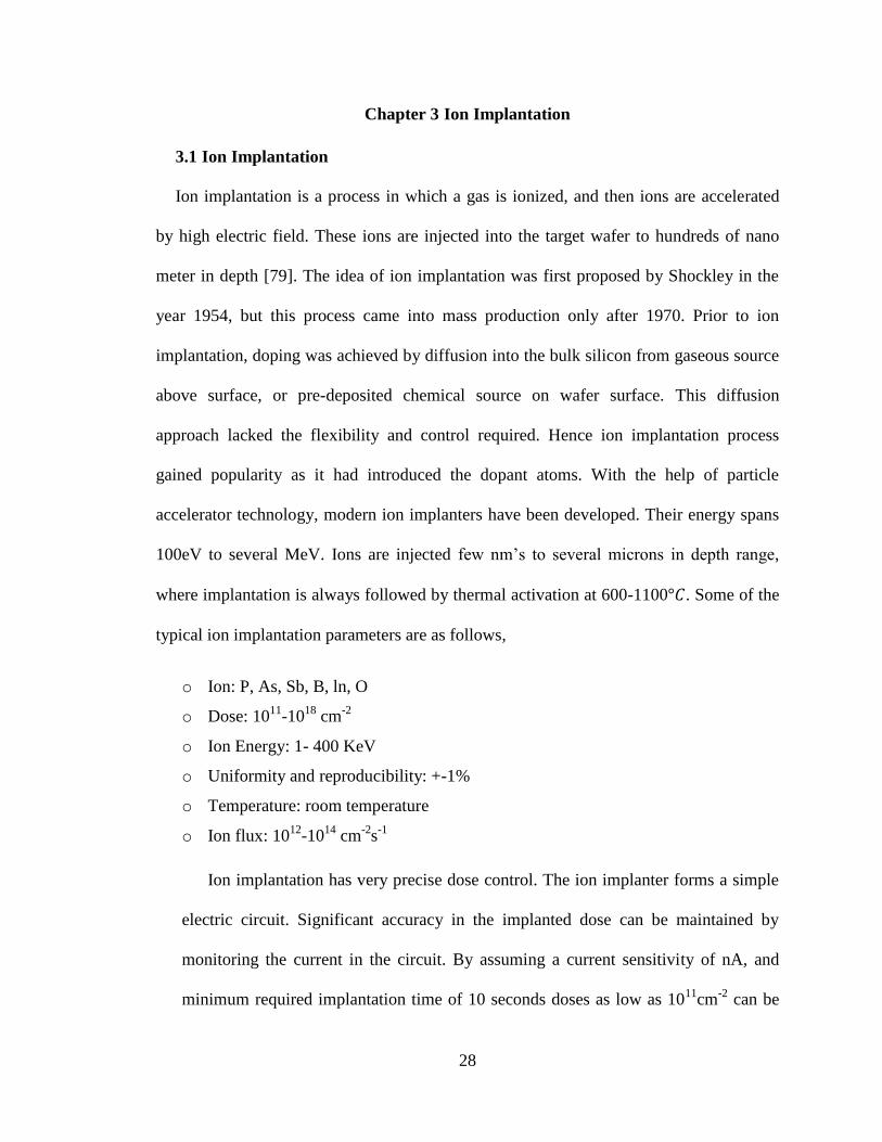
3.1 Ion Implantation
Ion implantation is a process in which a gas is ionized, and then ions are accelerated
by high electric field. These ions are injected into the target wafer to hundreds of nano
meter in depth [79]. The idea of ion implantation was first proposed by Shockley in the
year 1954, but this process came into mass production only after 1970. Prior to ion
implantation, doping was achieved by diffusion into the bulk silicon from gaseous source
above surface, or pre-deposited chemical source on wafer surface. This diffusion
approach lacked the flexibility and control required. Hence ion implantation process
gained popularity as it had introduced the dopant atoms. With the help of particle
accelerator technology, modern ion implanters have been developed. Their energy spans
100eV to several MeV. Ions are injected few nm’s to several microns in depth range,
where implantation is always followed by thermal activation at 600-1100 . Some of the
typical ion implantation parameters are as follows,
o Ion: P, As, Sb, B, ln, O
o Dose: 1011
-1018
cm-2
o Ion Energy: 1- 400 KeV
o Uniformity and reproducibility: +-1%
o Temperature: room temperature
o Ion flux: 1012
-1014
cm-2
s-1
Ion implantation has very precise dose control. The ion implanter forms a simple
electric circuit. Significant accuracy in the implanted dose can be maintained by
monitoring the current in the circuit. By assuming a current sensitivity of nA, and
minimum required implantation time of 10 seconds doses as low as 1011
cm-2
can be

29
measured. This process is done in high vacuum and hence it’s a very clean process
step. In ion implantation beside the dose control, peak depth and spread range can
also be controlled which is way better then diffusion process.
Figure 3.1 (a) Doping by diffusion, (b) Doping by ion implantation
Figure 3.1 shows comparative doping process by diffusion (top) and doping by ion
implantation (bottom) and it shows how precisely doping is done in ion implantation.
Some of advantages of ion implantation are,
o It is a low temperature process,
o wide selection of masking materials,
o less sensitive to surface cleaning procedures,
o Very fast and complex profiles can be achieved by multi-energy implants.
30
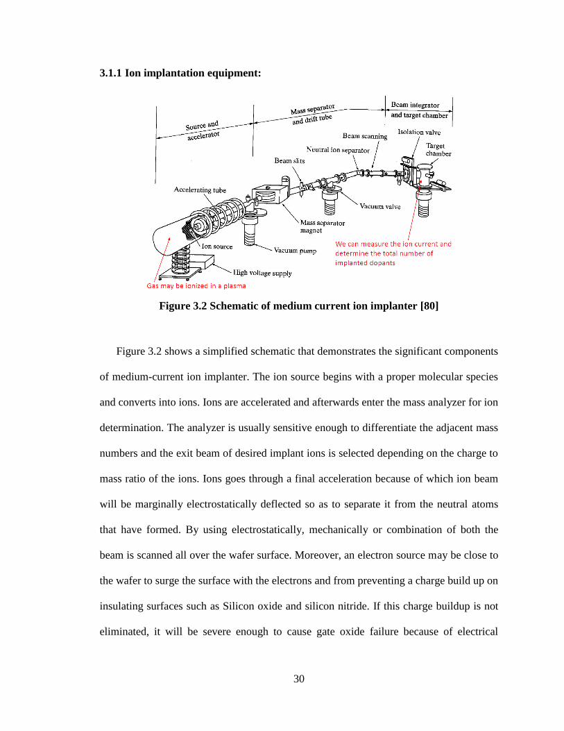
3.1.1 Ion implantation equipment:
Figure 3.2 Schematic of medium current ion implanter [80]
Figure 3.2 shows a simplified schematic that demonstrates the significant components
of medium-current ion implanter. The ion source begins with a proper molecular species
and converts into ions. Ions are accelerated and afterwards enter the mass analyzer for ion
determination. The analyzer is usually sensitive enough to differentiate the adjacent mass
numbers and the exit beam of desired implant ions is selected depending on the charge to
mass ratio of the ions. Ions goes through a final acceleration because of which ion beam
will be marginally electrostatically deflected so as to separate it from the neutral atoms
that have formed. By using electrostatically, mechanically or combination of both the
beam is scanned all over the wafer surface. Moreover, an electron source may be close to
the wafer to surge the surface with the electrons and from preventing a charge build up on
insulating surfaces such as Silicon oxide and silicon nitride. If this charge buildup is not
eliminated, it will be severe enough to cause gate oxide failure because of electrical

31
breakdown from gate to substrate through oxide. Some of the functions of various parts
of ion implanter are as follows:
1. Ion source: It usually operates at a subsequently high voltage (25 Kv) and
converts the electrically neutral dopant atoms in the gas phase into the plasma
ions and undesired species Sources such as arsine, phosphine, diborane can be
sputtered in ion sources.
2. Mass Spectrometer: In this, a magnet bends the ion beam into a right angle and
selects the desired impurity ion and removes undesired species. Ions which are
selected are passed through an aperture.
3. Accelerator: Adds energy to beam up to 5 MeV.
4. Scanning system: x-axis and y-axis deflection plated are used for scanning the
beam all over the wafer for the formation of uniform implantation of desired dose.
The beam is prevented in such a way that neutral particles are prevented from
hitting the target.
3.2 Impurity distribution equation:
Each ion in the ion implantation travels in some random path as it has to penetrate
the target. Hence, it loses its energy because of nuclear and electronic stoppage. The
doses used in implantation are generally higher than 1012
ions/cm3. Trajectories of the
ions can be predicted with the help of statistical means. By composing both lateral and
vertical motions the average total path length is determined which is called as range R.
The projected range Rp is the average depth of implanted ions. By using Gaussian

32
distribution of implanted ions, the depth can be approximated with standard deviation p
(or Rp). The ion concentration N(x), at depth x is given by the expression [81],
(3.1)
Where,
Np is the peak concentration,
Rp is projected range
p is standard deviation
If the total implanted dose is , by integrating the above equation we get the
expression for peak concentration Np which can be given as [82],
√ (3.2)
Generally, moments are considered to characterize the arbitrary distribution.
a) Dose, is considered as the zeroth moment.
b) The projected range Rp is considered as the normalized first moment.
c) The second moment is the standard deviation p.
d) The third moment is considered to be skewness , which is a measure of
asymmetry of the distribution. If the skewness is positive than the peak of the
distribution is placed closer to the surface other than projected range. Typically
the value of skewness is 0.
e) The last and fourth moment is kurtosis which is expressed by Kurtosis
indicates the top flatness of the distribution which is 3 for true Gaussian
distribution.
The above parameters can be illustrated schematically with the help of the figure below,

33
Figure 3.3 Schematic for the ion range [83]
In the Figure 3.1 i.e., (a) it is clear that the total path length R is longer than the
projected Rp. The bottom part (b) shows the stopped atom distribution is two-dimensional.
There are lots of different distributions which have been employed to give more
precise fit to moments of ion implantation which is possible using a Gaussian of which
the most important is Pearson IV fit. The fitted distributions for energies between 30 KeV
and 800 KeV is compared for experimental boron profiles under non channeling
conditions in the figure given as,
34
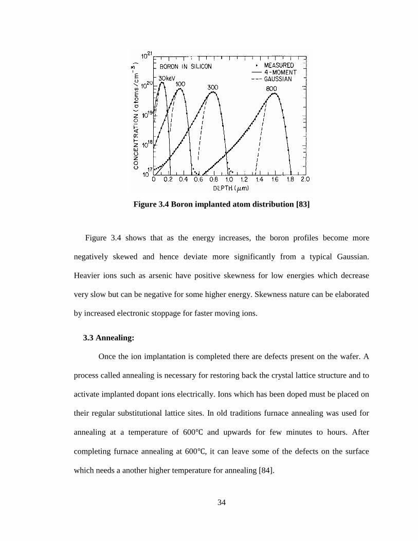
Figure 3.4 Boron implanted atom distribution [83]
Figure 3.4 shows that as the energy increases, the boron profiles become more
negatively skewed and hence deviate more significantly from a typical Gaussian.
Heavier ions such as arsenic have positive skewness for low energies which decrease
very slow but can be negative for some higher energy. Skewness nature can be elaborated
by increased electronic stoppage for faster moving ions.
3.3 Annealing:
Once the ion implantation is completed there are defects present on the wafer. A
process called annealing is necessary for restoring back the crystal lattice structure and to
activate implanted dopant ions electrically. Ions which has been doped must be placed on
their regular substitutional lattice sites. In old traditions furnace annealing was used for
annealing at a temperature of 600 and upwards for few minutes to hours. After
completing furnace annealing at 600 , it can leave some of the defects on the surface
which needs a another higher temperature for annealing [84].

35
Annealing process called rapid thermal annealing (RTA) has been applied more
recently in which arc and halogen lamps are used. This process is used for higher
temperatures greater than 1000 , for shorter anneal durations which is in seconds. Using
the same RTA equipment spike annealing is carried out which is applied to minimise the
diffusion. The dwell time is zero at maximum temperature for spike annealing which uses
rapid up and down rates.
Annealing processes are carried out in a heat balance regime where the
equilibrium between power deposited and lost power is maintained. This results in a
steady state heat balance throughout the wafer with a time scale equivalent to t>10-2
s.
Flash annealing is one of the type of annealing where a short pulse (10-6
<t<10-2
s) will
rapidly raise the temperature which comes out of a flash lamp known as thermal flux
regime. Pulsed layers are capable of producing a rapid heat of the surface layers with
times of 10-11
to 10-6
s which is known as adiabatic regime and effects the near surface
only. With the help of pulsed lasers it is possible to regrow the surface region by liquid
phase epitaxy or in the sub melt region by solid phase epitaxy.
Generally in the device production most common annealing is either spike or
rapid thermal annealing. But for shallower junctions different annealing methods such as
laser annealing comes into picture.
3.4 Fabrication process of MESFET:
There is a standard operating procedure followed for fabricating a MESFET. Steps
involving the fabrication of MESFET are as follows [85]:
o Intially the wafer is inspected and cleaned.
o Gallium Nitride cap is deposited by process called reactive sputtering.

36
o Positive resist is used for the channel implantation.
o Deep etching of gallium nitride is done by alignment registration process.
o Stripping and ashing is done on oxygen plasma.
o Using a positive resist source and drain are implanted by resist patterning.
o Ion implantation for the device source and drain regions is done.
o Resist the stripping and ashing of O2 plasma.
o Using the rapid thermal annealing, ion implants should be annealed.
o Resist patterning for ohmic contact formations.
o Ethcing of gallium nitride for the formation of ohmic contacts.
o Depositing GaN metal for ohmic contacts to source and drain using d-beam
evaporation and patterning by using process called litoff technique.
o Thermal heating is done on ohmic contact.
o Schottky gate is formed by resisting the pattern of etched nitride.
o Etching for forming Schottky gate.
o Metal depostion for schottky gate formation using e-beam lift-off technique.
Basically, fabricating of GaN is done by four mask ,double ion implanatation which
can be seen in the figure below:
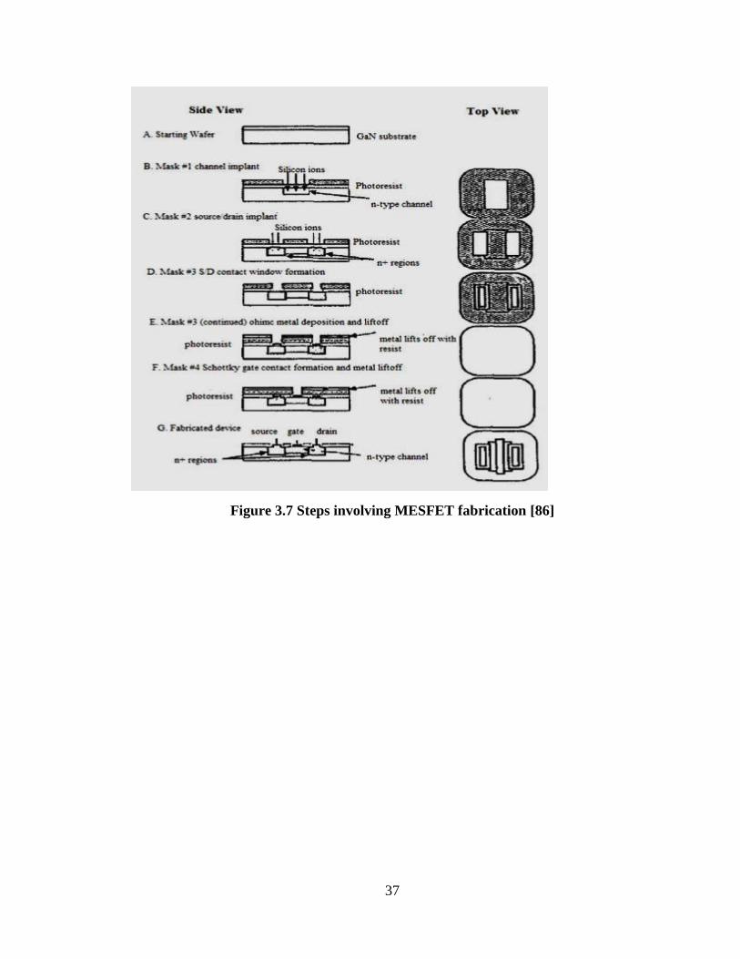
37
Figure 3.7 Steps involving MESFET fabrication [86]

38
Chapter 4 Physics of MESFET
4.1 MESFET:
MESFET is a shortened form for metal-semiconductor field effect transistor. It is
a unipolar device where the current conduction happens by flow of majority carriers
only. MESFET can be either n-type or a p-type. In an n-type MESFET current
conduction is due to flow of electrons, while in a p-type MESFET holes cause the current
conduction. MESFET comprises of a conducting channel through which the device
conducts electricity. This channel is positioned between source and drain contacts, as
illusttrated in Figure 4.1 below. The flow of free carriers, and consequently the current
through the channel is controlled by modifying the gate voltage. This results in the
thickness of the consumption layer underneath the metal contact. The Schottky barrier is
a potential enegy barrier for electrons formed st metal-semiconductor junction. Schottky
barriers have rectifying characteristics, suitable for use as a diode.
Figure 4.1: Schematic representation of Gallium Nitride MESFET [87]
39
4.2 Working of MESFET:
Figure 4.1 shows a MESFET which includes 3 terminals, called as gate, source
and drain. A semi-protecting GaN substrate is utilized underneath the conduction
channel. The n-doped area, which acts as a channel can be framed in two ways, by ion
implantation or by developing an epitaxial layer. As mentioned before ion implantation
includes ion dispersion in the slight n-doped layer, epitaxial growth is a methodology
where crystals are developed in a specific introduction over another crystal. [88]. If both
crystals are of the same material, the methodology is known as homoepitaxy, and if the
materials are different, it is known as heteroepitaxy. n+ doped area are embedded on both
sides of the n-doped channel and are termed source and drain. Metal contacts are then set
on top of the gate, source and drain forming three unique terminals for a MESFET. The
gate metal and n-doped material forms a Schottky barrier [89].
4.2.1 Types of MESFETS and its operations:
There are two types of MESFETs as explained beloe:
Enhancement MESFET:
In an n channel MEFET the device remains switched off and the channel region is
maturely covered by depletion region completely. This depletion region is narrowed so
that the channel region gets expanded. This facilitates the flow of carriers. A junction
between the channels is forward bias and gate is made by applying positive voltage to the
gate terminal. The device conducts with the increase in channel width allowing the
current to flow. [90].
40
Figure 4.2: E-MESFET [91]
Depletion MESFET:
In an n-channel depletion MESFET (as shown in Figure 4.3), the depletion width
is varied by varying voltage at the gate terminal. Applying a negative voltage at the gate-
to-source causes the depletion width to expand and make the channel width narrow,
obstructing the flow of carriers. As a result the junction between the gate and the drain
becomes reverse biased. If the depletion region is expanded such that it completely
blocks the channel, or pinches-off` the channel, the resistance of the channel from source
to drain becomes large, causing the MESFET to be turned off like a switch. Applying a
positive gate-to-source voltage minimizes depletion width and allows the channel size to
increase again turning the MESFET ON.
Figure 4.3: Depletion MESFET [92]
41
4.3 MESFET Characteristics:
4.3.1 I-V Characterisctics:
Current-Voltage characterisctic of MESFET is almost similar to that of MOSFET
and JFET. The ideal characteristics of a MESFET is shown in the below Figure 4.4:
Figure 4.4: Typical (I-V) characteristics of MESFET [93]
Figure 4.4 shows a typical drain current (Ids) with respect to drain source voltage
(Vds) characteristics. we realize that the drain current is additionally a capacity of gate-
source voltage (Vgs) so a singular curve. The Figure 4.4 shows the reliance of drain
current (Ids) in drain source voltage (Vds) for a specific quality of gate-source voltage
(Vgs). Above Figure 4.4 shows the I-V characteristics of an enhancement type MESFET.
In addition there is an alternate mode of operation in MESFET which is referred to as the
breakdown mode where extra drain source voltage is applied.
For operating a MESFET in a depletion mode a voltage has to be applied at the
gate terminal. By applying extra negative voltage at the increases depletion region and
the junction is reverse biased. The drain gets completely exhausted, in the event that
continue expanding the negative voltage at gate terminals Hence there is no flow of
42
current and leads to threshold voltage which can be defined as the voltage completely
deplete the fully doped channel layer [94]. Figure 4.4 shows that Id value decreases as the
gate source voltage decreases further increasing negative voltage on the gate terminal will
stop the channel completely. In this way it is clear that threshold voltage of the Figure 4.4
is near to the lowest Vgs curve.
4.3.2 Operating Regions in MESFET:
MESFET is operated in different regions, which can be illustrated as follows:
Linear Region: In the linear operating region the voltage Vds is expected to be very
small. Hence the current and voltage in this region behave in a linear fashion. Therefore
the drain current Ids is proportional to the drain source voltage Vds, when Vds is in a low
range [95].
Figure 4.5: I-V chadracteristics in a linear or active region [96]

43
Saturation Region: In the linear region, drain-source current Ids is directly proportional
to the source drain voltage Vds but after further increasing the voltage Vds there is not that
much change in the drain-source current Ids. Therefore a saturation drain current is
achieved when source-drain voltage equals the drain voltage(ie, Vds=Vd) . This depletes
the channel length resulting an increase in the drain current Id.
Figure 4.6: Drain-source current vs drain-source voltage in saturation region [97]
4.4 MESFET applications in various fields:
Various fabrication methods have been applied for fabricating MESFET for use in
different variety of semiconductor systems. Of this some of the main applications of
MESFET for numerous purposes such as:
o Military applications, where MESFET is applied in various secured
communicating equipment.
o As there is an increase in the telecom industry now a days MESFET is playing an
important role in manufacturing of low power RF amplifiers which is reducing the
manufacturing costs.
o In the high frequency applications for example RADAR and satellite
communication MESFET is an important electronic device.
44
o In the microwave links MESFET can be used as a power amplifier for the output
stages.
o It is also used as a power oscillator in some areas and had a wide application in
commercial optoelectronics. [98]
45
Chapter 5 Theory and Calculations
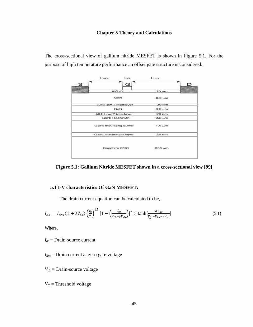
The cross-sectional view of gallium nitride MESFET is shown in Figure 5.1. For the
purpose of high temperature performance an offset gate structure is considered.
Figure 5.1: Gallium Nitride MESFET shown in a cross-sectional view [99]
5.1 I-V characteristics Of GaN MESFET:
The drain current equation can be calculated to be,
(
)
(
)
(5.1)
Where,
Ids = Drain-source current
Idss = Drain current at zero gate voltage
Vds = Drain-source voltage
Vth = Threshold voltage

46
Vgs = gate-source voltage
T = Temperature in kelvin
T0 = Room temperature which is 300k
The drain current at zero gate voltage can be defined by following equation,
[
[ ( )]]
(5.2)
Where,
ha = Depletion region width
Ifc = Full saturation current
Vp = Pinch-off voltage
Qa = Conducting channel charge
Nd = Donor concentration
Vbi = Built in voltage
Vgs = gate-source voltage
5.2 Trans-conductance of GaN MESFET:
The quality of a device is mainly determined by trans-conductance. The equation
of trans-conductance is given by following equation,
(
)
(
)
( ) (
) (5.3)
Where,
gm = trans-conductance
47
Ids = Drain-source current
Vgs = gate-source voltage
Vth = Threshold voltage
Vds = Drain-source voltage
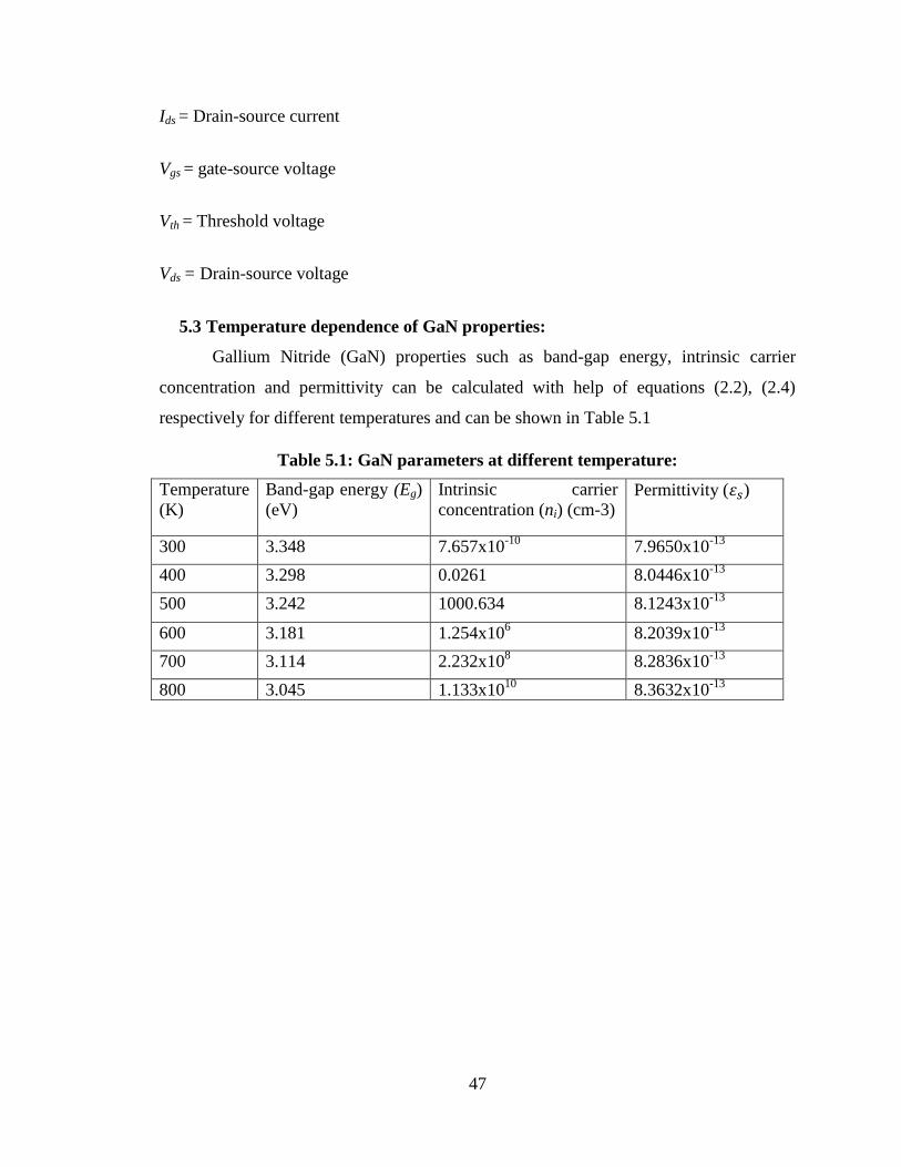
5.3 Temperature dependence of GaN properties:
Gallium Nitride (GaN) properties such as band-gap energy, intrinsic carrier
concentration and permittivity can be calculated with help of equations (2.2), (2.4)
respectively for different temperatures and can be shown in Table 5.1
Table 5.1: GaN parameters at different temperature:
Temperature
(K)
Band-gap energy (Eg)
(eV)
Intrinsic carrier
concentration (ni) (cm-3) Permittivity ( )
300 3.348 7.657x10⁻¹⁰
7.9650x10⁻¹³
400 3.298 0.0261 8.0446x10⁻¹³
500 3.242 1000.634 8.1243x10⁻¹³
600 3.181 1.254x10⁶ 8.2039x10
-13
700 3.114 2.232x10⁸ 8.2836x10
-13
800 3.045 1.133x10¹⁰
8.3632x10⁻¹³
48
Chapter 6 Results and Discussion
A physics based analytical model of GaN based MESFET has been developed to
study the temperature effect on drain current and transconductance. The intrinsic carrier
concentration shows a value in the order of 1x10⁻⁹
cm-3
at 300K whereas the value of
silicon and GaAs materials show in the order of 1010
cm-3
and 106cm
-3. Hence, the GaN
based device shows no detrimental performance at the high temperature range of 800k -
900K. Hence the some electrical parameters such as I-V characteristics and
transconductance have been computed and the temperature effect on the device
performance has been established through the following results. The analytical model
incorporates the temperature dependence intrinsic carrier concentration, bandgap energy,
permittivity of GaN material and detailed properties are shown in Table 3.1.
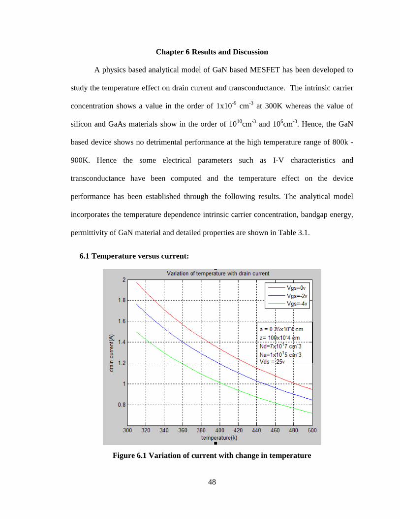
6.1 Temperature versus current:
Figure 6.1 Variation of current with change in temperature

49
The Figure 6.1 shows a plot of drain current versus temperature for different gate-source
voltage of Vgs = 0V, -2V and -4V with constant drain-source voltage of Vds = 25V,
channel doping concentration of Nd = 7x10¹⁷
cm-3
, substrate doping of Na = 1x10¹⁵
cm-3
,
gate length of L = 0.25x10⁻⁴
cm, device width of Z = 100x10-4
cm and active channel
thickness of a = 0.25x10⁻⁴
cm. Different drain currents are found to be 1.98 A, 1.76 A and
1.52 A at 300K for the gate-source voltage Vgs = 0V, -2V and -4V, respectively. The
drain currents are observed to be exponentially dropped to the approximate value of 0.7
A, 0.86 A and 0.96 A, when the temperatures reaches tot 500K. Hence, the value of the
drain current does not change significantly due to the change of temperature from 300K
to 500K. This graph has been generated by using the Equation (5.1).
6.2 I-V characteristics:
Figure 6.2: Ids versus Vds plot by giving different gate source voltage Vgs

50
The Figure 6.2 presents a graph of drain current (Ids) versus drain-source voltage
(Vds) for different gate-source voltage of Vgs = 0V, -2V, and -4V with channel doping
concentration of Nd = 7x10¹⁷
cm-3
, substrate doping of Na = 1x10¹⁵
cm-3
, gate length of L
= 0.25x10⁻⁴
cm, device width of Z = 100x10-4
cm and active channel thickness of a =
0.25x10⁻⁴
cm. The drain currents of 1.5A for different Vgs clearly show linearity up to
Vds = 20V, whereas the non-linearity of average current range from 1.65A to 2.4A is
observed for the drain-source voltage range of 20V to 50V. Three currents for different
Vgs become saturated at 2.65A, 2.55A and 2.45A, when the drain-source voltage appears
to 100V. This plot has been generated using the Equation (5.1) to find the I-V
characteristics at 300K.
6.3 I-V characteristics for different active channel thickness (a):
Figure 6.3: Ids versus Vds plot for different active channel thickness.

51
The Figure 6.3 exhibits a graph of drain current (Ids) versus drain-source voltage
(Vds) for different active channel thickness of a = 0.2x10⁻⁴
cm, 0.25x10⁻⁴
cm, 0.3x10⁻⁴
with channel doping concentration of Nd = 7x10¹⁷
cm-3
, substrate doping of Na = 1x10¹⁵
cm-3
, gate length of L = 0.25x10⁻⁴
cm, device width of Z = 100x10-4
cm and constant gate
to source voltage of Vgs = 0 V. The drain currents clearly show the linearity, non-linearity
and saturation regimes. The plot shows that the maximum current is obtained for large
active thickness of 3x10⁻⁴
cm. The pinch-off voltage is found in the order of 35V, 25V
and 15V for the active channel thickness of 3x10⁻⁴
cm, 2.5x10⁻⁴
cm and 2x10⁻⁴
cm
respectively.
6.4 Transconductance by varying temperature:
Figure 6.4 Variation of Transconductance with Temperature:
52
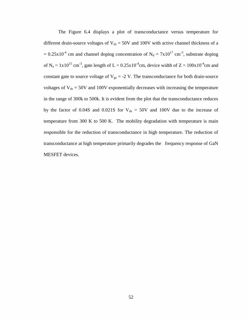
The Figure 6.4 displays a plot of transconductance versus temperature for
different drain-source voltages of Vds = 50V and 100V with active channel thickness of a
= 0.25x10⁻⁴
cm and channel doping concentration of Nd = 7x10¹⁷
cm-3
, substrate doping
of Na = 1x10¹⁵
cm-3
, gate length of L = 0.25x10⁻⁴
cm, device width of Z = 100x10-4
cm and
constant gate to source voltage of Vgs = -2 V. The transconductance for both drain-source
voltages of Vds = 50V and 100V exponentially decreases with increasing the temperature
in the range of 300k to 500k. It is evident from the plot that the transconductance reduces
by the factor of 0.04S and 0.021S for Vds = 50V and 100V due to the increase of
temperature from 300 K to 500 K. The mobility degradation with temperature is main
responsible for the reduction of transconductance in high temperature. The reduction of
transconductance at high temperature primarily degrades the frequency response of GaN
MESFET devices.

53
Chapter 7 Conclusion
An analytical model of GaN MESFET has been developed to simulate the
temperature dependent drain current and transconductance. The drain current drops to
1A, 0.9 and 0.82 for gate-source voltage Vgs = 0V, -2V and -4V for a temperature
variation from 300 K to 500 K. The transconductance also falls with a factor of 0.04S and
o.021S for the temperature variation from 300 K to 500 K. All I-V characteristics clearly
show the linearity regime, non-linear regime and saturation regime to justify the validity
of the model. The computed results show that the drain current and transconductance
have very insignificant variation on the device performance. Hence, GaN MESFET
shows incredible thermal stability at extreme high temperatures. The scope of the
research shows tremendous potential for developing high temperature stable FET using
GaN material. This will be a very attractive arena for withstanding at high temperatures,
harsh environment suitable to military, aerospace and space exploration.

54
References
[1] A.S.Barker,M.Ilegems “Phys. Rev. B (USA)” vol.7(1973)p.743.
[2] Stephen Pearton, Gerhard Fasol, “The Blue Laser Diode: The Complete Story”.
NewYork: Springer, 2000
[3] C. Gaquiere, S. Trassaert, B. Boudart, and Y. Crosnier “High-Power GaN
MESFET on Sapphire Substrate” –IEEE MICROWAVE AND GUIDED WAVE
LETTERS, VOL. 10, NO. 1, JANUARY 2000
[4] Khan M A, Kuznia J N, Olson D T, Van Hove J M and Blasingame M- 1992
Appl. Phys. Lett. 60 2917
[5] R.J. Trew, M.W. Shin and V. Gatto “Wide Bandgap Semiconductor Electronic
Devices for High Frequency Applications” – Gallium Arsenide Integrated Circuit
(GaAs IC) Symposium, 1996. Technical Digest 1996., 18th Annual
[6] S. J. Pearton, J. C. Zolper, R. J. Shul, and F. Ren J. “GaN: Processing, defects,
and devices” - Appl. Phys. 86, 1 (1999)
[7] C. A. Liechti –“Microwave field-effect transistors-1976”, IEEE Trans.
Microwave Theory Tech., vol. MTT-24, no. 6, pp. 279-299, June 1976.
[8] Khan M A, Kuznia J N, Olson D T, Van Hove J M and Blasingame M 1992 Appl.
Phys. Lett. 60 2917
[9] Khan M A, Kuznia J N, Olson D T, Blasingame M and Bhattarai A R 1993 Appl.
Phys. Lett. 63 2455
[10] Khan M A, Kuznia J N, Bhattarai A R and Olson D T 1993 Appl. Phys. Lett. 62
1786

55
[11] Khan M A, Bhattarai A, Kuznia J N and Olson D T 1993 Appl. Phys. Lett. 63
1214
[12] Pat Hindle, Future RF market opportunities for GaN, june 12 2012
[13] Pankove J, Chang S S, Lee H C, Molnar R J, Moustakas T D and Van
Zeghbroeck B 1994 IEDM 94-389
[14] Lin M E, Ma Z, Huang F Y, Fan Z F, Allen L H and Morko¸c H 1994 Appl.
Phys. Lett. 64 1003
[15] Ping A T, Khan M A and Adesida I 1996 J. Electron. Mater. at press
[16] Tigran T Mnatsakanova, Michael E Levinshtein- “Carrier mobility model for
GaN- Solid-State Electronics” - Volume 47, Issue 1, January 2003, Pages 111–
115
[17] Ulf Gustavsson, Thomas Lejon, Christian Fager, Herbert Zirath “Design of highly
efficient, high output power, L-band class D−1 RF power amplifiers using GaN
MESFET devices” - 37th European Microwave Conference, Munich, Germany
[18] S. Azam, R. Jonsson and Q. Wahab “Designing, Fabrication and Characterization
of Power Amplifiers Based on 10-Watt SiC MESFET & GaN HEMT at
Microwave Frequencies”- , 38th European Microwave Conference, Amsterdam,
The Netherlands
[19] S. N. Mohammad, M. S. Unlu, and H. Morkoq, “Optically controlled current-
voltage characteristics of ion-implanted MESFETs” Solid-State Electron., vol. 33,
no. 12, pp. 1499-1509, 1990.
[20] Syed S. Islam and A. F. M. Anwar – “Nonlinear Analysis of GaN MESFETs With
Volterra Series Using Large-Signal Models Including Trapping Effects” IEEE

56
TRANSACTIONS ON MICROWAVE THEORY AND TECHNIQUES, VOL.
50, NO. 11, NOVEMBER 2002
[21] Y. Dora, A. Chakraborty, S. Heikman, L. McCarthy, S. Keller, and U. K. Mishra
“Effect of Ohmic Contacts on Buffer Leakage of GaN Transistors” -– IEEE
ELECTRON DEVICE LETTERS, VOL. 27, NO. 7, JULY 2006 529
[22] “ATIP07.033: GaN Amplifiers for RF Communications in Japan” - ATIP
Document ID: 071010R
[23] R. Gaska, M. Asif Khan, X. Hu, G. Simin, and J. Yang – “GaN-based MESFETs
and DC-MOSFETs” Device Research Conference, 2000. Conference Digest. 58th
DRC
[24] Binari S C, Dietrich H B, Kelner G, Rowland L B, Doverspike K and Gaskill D K
1994 Electron. Lett. 30 909
[25] S. Müller, K. Köhler, R. Kiefer, R. Quay, M. Baeumler, and L. Kirste- “Growth
of AlGaN/GaN based electronic device structures with semi-insulating GaN
buffer and AlN interlayer”- 2005 WILEY-VCH Verlag GmbH & Co. KGaA,
Weinheim
[26] Medjdoub, F. – “Sub-1-dB Minimum-Noise-Figure Performance of GaN-on-Si
Transistors Up to 40 GHz” - Electron Device Letters, IEEE (Volume:33 , Issue:
9 )
[27] Hidenori Shimawaki and Hironobu Miyamoto, “GaN-based FETs for Microwave
High-Power Applications” - 13th
GAAS Symposium, Paris 2005
57
[28] M.W. Shin and R.J. Trew, “GaN MESFETs for high-power and high temperature
microwave applications” -ELECTRONICS LETTERS 16th March 1995 Vol. 31
No. 6
[29] Tzu-Jin Yeh, Yi-Jen Chan and Tien-Huat, “Ion-implanted GaAs MESFET's with
W/WNx Bi-layer Gate Designs” - Gan EDMS'94
[30] Maziar Farahmand and Kevin F. Brennan “Full Band Monte Carlo Simulation of
Zincblende GaN MESFET’s Including Realistic Impact Ionization Rates” IEEE
TRANSACTIONS ON ELECTRON DEVICES, VOL. 46, NO. 7, JULY 1999
[31] Won Sang Lee, Yoon Ho Chi, Ki Wong Chung, Dong Chan Moon and Moo
Whan Shin- “Performance of GaN MESFETs with an Undoped Highly Resistive
Buffer Layer” Journal of the Korean Physical Society, Vol. 38, No. 2, February
2001, pp. 146- 150
[32] Maziar Farahmand – “Comparison between Wurtzite Phase and Zincblende Phase
GaN MESFET’s Using a Full Band Monte Carlo Simulation” IEEE
TRANSACTIONS ON ELECTRON DEVICES, VOL. 47, NO. 3, MARCH 2000
[33] Makarov, D.G. Krizhanovski, V.G., Kistchinsky, A. “A. GaN class E wideband
microwave power amplifier” - 18th International Conference on Microwave
Radar and Wireless Communications (MIKON), 2010
[34] C. Gaquiere, S. Trassaert, B. Boudart, and Y. Crosnier “High-Power GaN
MESFET on Sapphire Substrate” –IEEE MICROWAVE AND GUIDED WAVE
LETTERS, VOL. 10, NO. 1, JANUARY 2000
[35] “Gallium Nitride (GaN) Microwave Transistor Technology For Radar
Applications”- Aethercomm

58
[36] C. Lee, W. L ua, E. Piner, I. Adesida – “DC and microwave performance of
recessed-gate GaN MESFETs using ICP” -RIE Solid-State Electronics 46 (2002)
743–746
[37] C. Gaquiere, S. Trassaert, B. Boudart, and Y. Crosnier – “High-Power GaN
MESFET on Sapphire Substrate” IEEE MICROWAVE AND GUIDED WAVE
LETTERS, VOL. 10, NO. 10, JANUARY 2000
[38] Umesh K. Mishra – “Gallium Nitride Electronics: Watt is the limit?”- Device
Research Conference, 2004. 62nd DRC. Conference Digest
[39] Sebastien Nuttinck, Edward Gebara, Joy Laskar, “Study of Self-Heating Effects,
Temperature-Dependent Modeling, and Pulsed Load–Pull Measurements on GaN
HEMTs” - IEEE TRANSACTIONS ON MICROWAVE THEORY AND
TECHNIQUES, VOL. 49, NO. 12, DECEMBER 2001
[40] Syed S. Islam, Member, A. F. M. Anwar and Richard T. Webster “A Physics-
Based Frequency Dispersion Model of GaN MESFETs” - IEEE
TRANSACTIONS ON ELECTRON DEVICES, VOL. 51, NO. 6, JUNE 2004
[41] Roberto Cuerdo, Eugenio Sillero, María Fátima Romero, Michael J. Uren,Marie-
Antoinette di Forte Poisson, Elías Muñoz and Fernando Calle “High-Temperature
Microwave Performance of Submicron AlGaN/GaN HEMTs on SiC” - IEEE
ELECTRON DEVICE LETTERS, VOL. 30, NO. 8, AUGUST 2009
[42] Siddharth Rajan, Huili Xing, Steve DenBaars, and Umesh K. Mishra
“AlGaN/GaN polarization-doped field-effect transistor for microwave power
applications” - APPLIED PHYSICS LETTERS VOLUME 84, NUMBER 9 1
MARCH 2004

59
[43] S. T. Sheppard, R. P. Smith, W. L. Pribble, Z. Ring, T. Smith, S. T. Allen, J.
Milligan and J. W. Palmour “High Power Hybrid and MMIC Amplifiers Using
Wide-Bandgap Semiconductor Devices on Semi-insulating SiC Substrates”- -
60th
Annual Device Research Conference, University of California--Santa
Barbara, June 2002
[44] Y.-F. WU, B. P. KELLER, S. KELLER, D. KAPOLNEK, P. KOZODOY, S. P.
DENBAARS and U. K. MISHRA, “HIGH POWER A1GaN/GaN HEMTs FOR
MICROWAVE APPLICATIONS”- Solid-State Electronics Vol. 41, No. 10, pp.
1569-1574, 1997
[45] Jong-Wook Kim, Jae-Seung Lee, Won-Sang Lee, Jin-Ho Shin, Doo-Chan Jung,
Moo-Whan Shin, Chang-Seok Kim, Jae-Eung, Jung-Hee Lee, Sung- Ho Hahm
“Microwave performance of recessed gate Al0.2Ga0.8N/GaN HFETs fabricated
using a photoelectrochemical etching technique” - Materials Science and
Engineering B95 (2002) 73-76
[46] Y.-F. Wu, D. Kapolnek, J. Ibbetson, N.-Q. Zhang, P. Parikh, B. P. Keller, and U.
K. Mishra, “High Al-content AlGaN/GaN HEMT on SiC substrates with very-
high power performance” in Proc. Int. Electron Device Meeting, 1999, pp. 925–
927.
[47] Kristoffer Andersson, Vincent Desmaris, Joakim Eriksson, Niklas Rorsman and
Herbert Zirath- “C-band Linear Resistive Wide Bandgap FET Mixers” IEEE 2003
IEEE MTT-S Digest
[48] G. E. Ponchak, Metal–Semiconductor Field-Effect Transistors (MESFETs)

60
[49] R.W. H. Engelmann and C. A. Liechti, Gunn domain formation in the saturated
current region of GaAs MESFETs, IEDM Tech. Dig., pp. 351-354, Dec 1976.
[50] Stephen Pearton, Gerhard Fasol, The Blue Laser Diode: The Complete Story.
NewYork: Springer, 2000
[51] Edward T. Yu, III-V Nitride Semiconductors: Applications and Devices,NY:2003
[52] E.T. Yu and M.O. Manasreh III-V Nitride Semiconductors Applications and
Devices 2003
[53] Bougrov V., Levinshtein M.E., Rumyantsev S.L., Zubrilov A., “Band gap energy
Vs Temperature for Wurtzite GaN” in Properties of Advanced
SemiconductorMaterials GaN, AlN, InN, BN, SiC, SiGe . Eds. Levinshtein M.E.,
Rumyantsev S.L., Shur M.S., John Wiley & Sons, Inc., New York, 2001, 1-30
[54] C. A. Liechti, Microwave field-effect transistors-1976, IEEE Trans. Microwave
Theory Tech., vol. MTT-24, no. 6, pp. 279-299, June 1976.
[55] Simon M. Sze; Ming-Kwei Lee Semiconductor Devices: Physics and Technology
John Wiley & Sons
[56] R. W. H. Engelmann, Low noise Schottky barrier FET transistor (InP), Hewlett-
Packard Laboratories, Semiannual Rep. ECOM-Rep. ECOM-75-1300-F, Apr.
1976.
[57] R. W. H. Engelmann and C.A. Liechti, Bias dependence of GaAs and InP
parameters, IEEE Trans. Electron Devices, vol. ED-24, pp. 1288-1296, Nov.
1977.
61
[58] K. Yamaguchi, S. Asai, and H. Kodera, Two-dimensional numerical analysis of
stability criteria of GaAs FETs, IEEE Trans. Electron Devices, vol. ED-23, pp.
1283-1290, Dec. 1976.
[59] M. S. Shur and L. F. Eastman, Current-voltage characteristics, small-signal
parameters, and switching times of GaN FET’s this issue, pp. 606-611.
[60] W. Shockley, A unipolar field-effect transistor, Proc. IRE, vol. 40, p. 1365,1952.
[61] A. S. Grove, Physics and Technology of semiconductor Devices. New York:
Wiley, 1967.
[62] C. Tsironis and H. Beneking, Avalanche noise in GaAs MESFETs,Electron. Lett.,
vol. 13, no. 15, pp. 438-439, 1977.
[63] M. P. Shaw, P.R. Solomon, and H. L. Grubin, The influence of boundary
conditions on current unstabilities in GaN, IBM J. Res. Develop., vol. 13, no. 5,
pp. 587-590, 1969.
[64] T. Turner and B. Wilson, Implications of carrier velocity saturation in a gallium
arsenide field-effect transistor, in Proc. 1968 Symp. GaAs. (London: Inst. Phys.,
Conf. Series No. 7, 1969), pp.195-204.
[65] K. Lehovec and R. Zuleeg, Voltage-current characteristics of GaAs J-FET’s in the
hot electron range, Solid-State Electron., vol. 13, pp. 1415-1426, Oct. 1970.
[66] P. Hower and G. Bechtel, Current saturation and small-signal characteristics of
GaN field-effect transistors, IEEE Trans. Electron Devices, vol. ED-20, pp. 213-
220, Mar. 1973.
[67] C. A. Liechti, Microwave field-effect transistors-1976, IEEE Trans. Microwave
Theory Tech., vol. MTT-24, no. 6, pp. 279-299, June 1976.

62
[68] K. E. Drangeid, R. F. Broom, W. Jutzi, T. O. Mohr, A. Moser, and G. Sasso, “A
memory-cell array with normally off-type Schottky-barrier FETs”, IEEE J. Solid-
State Circuits, vol. SC-7, pp. 277-287, Aug. 1972.
[69] H. Ishikawa, H. Kusakawa, S. Katsuhiko, and F. Masumi, “Normally-off type
GaN MESFET for low power, high speed logic circuits” ISSCC Dig. Tech.
Papers, pp. 200-201, Feb. 1977
[70] D. H. Claxton, “TED/FET monolithic microwave integrated circuits” in Proc.
1977 Device Res. Conf. (Cornell University, Ithaca, NY, June 27-29, 1977).
[71] R. L. Van Tuyl and C. A. Liechti, “Gallium arsenide spawns speed, IEEE
spectrum,” pp. 41-48, Mar. 1977.
[72] Turner and B. Wilson, “Implications of carrier velocity saturation in a gallium
arsenide field-effect transistor,” in Proc. 1968 Symp. GaAs. (London: Inst. Phys.,
Conf. Series No. 7, 1969), pp.195-204.
[73] K. Lehovec and R. Zuleeg, “Voltage-current characteristics of GaAs J-FET’s in
the hot electron range,” Solid-State Electron., vol. 13, pp. 1415-1426, Oct. 1970.
[74] P. Hower and G. Bechtel, “Current saturation and small-signal characteristics of
GaN field-effect transistors,” IEEE Trans. Electron Devices, vol. ED-20, pp. 213-
220, Mar. 1973.
[75] C. A. Liechti, “Microwave field-effect transistors-1976,” IEEE Trans. Microwave
Theory Tech., vol. MTT-24, no. 6, pp. 279-299, June 1976.
[76] K. E. Drangeid, R. F. Broom, W. Jutzi, T. O. Mohr, A. Moser, and G. Sasso, “A
memory-cell array with normally off-type Schottky-barrier FETs,” IEEE J. Solid-
State Circuits, vol. SC-7, pp. 277-287, Aug. 1972.

63
[77] H. Ishikawa, H. Kusakawa, S. Katsuhiko, and F. Masumi, “Normally-off type
GaN MESFET for low power, high speed logic circuits,” in ISSCC Dig. Tech.
Papers, pp. 200-201, Feb. 1977
[78] D. H. Claxton, “TED/FET monolithic microwave integrated circuits,” in Proc.
1977 Device Res. Conf. (Cornell University, Ithaca, NY, June 27-29, 1977).
[79] R. L. Van Tuyl and C. A. Liechti, “Gallium arsenide spawns speed,” IEEE
spectrum, pp. 41-48, Mar. 1977.
[80] Figge, S., Böttcher, T., Dennemarck, J., Kröger, R., Paskova, T., et al. (2005).
“Optoelectronic devices on bulk GaN. Journal of Crystal Growth”, 281(1), 101-
106.
[81] Nakamura, S., Senoh, M., Nagahama, S., Iwasa, N., Yamada T., et al. (1996).
“InGaN-based multi-quantum-well-structure laser diodes. Japanese Journal of
Applied” Physics, 35(1B), L74-L76.
[82] Potential Performance of SiC and GaN Based Metal Semiconductor Field
Effect transistorsH. Arabshahi Department of Physics, Ferdowsi University of
Mashhad, P.O. Box 91775-1436, Mashhad, Iran (Received on 23 July, 2008).
[83] A complete analytical model of GaN MESFET for microwave frequency
applications -S.Bose, Adarsh, A.Kumar, Simrata, M.Gupta, R.S. Gupta, Received
11 April 2001; revised 23 May 2001; accepted 4 June 2001.
[84] P. Kung, A. Saxler, X. Zhang, D. Walker, R. Lavado, M. Razaghi, Appl. Phys.
Lett.69(1996)2116
[85] W. Gotz, L.T. Romano, J. Walker, N.M. Johnson, R.J. Molnar, Appl. Phys. Lett.
72 (1998).
64
[86] S. Fischer, A. Gisbertz, B.K. Meyer, M. Topf, S. Koynov, I. Dirnstorfer, D. Volm,
R. Ueckev, P. Reiche, Symp, Proc. Egn-1, 1996.
[87] O. Ambacher, J. Phys. D 31 (1998) 2653.
[88] M. Morita, S. Isogai, N. Shimizu, K. Tsubouchi, N. Mikohiba, Jpn. J. Appl. Phys.
19 (1981).
[89] Y. Kato, S. Kitamura, K. Hiramatsu, N. Sawaki, J. Cryst. Growth,144(1994)133
[90] J.M. Van Hove, R. Hickman, J.J. Klaassen, P.P. Chow, P.P. Ruden, Appl. Phys.
Lett.70(1997) 282
[91] B. S. Simpkins, E. T. Yu, P. Waltereit and J. S. Speck, ―Correlated scanning
Kelvin probe and conductive atomic force microscopy studies of dislocations in
gallium nitride,J. Appl. Phys. 94 (2003) 1448
[92] Microelectronics Journal 35 (2004) 117–123, Properties of wurtzite GaN
MESFETs studied by two-dimensional full band Monte Carlo approach
[93] Guha, S., And Bojarczuk, N.A.: Ultraviolet And Violet GaN Light Emitting
Diodes On Silicon', Appi. Phys. Lett. 1998, 72, Pp. 415417
[94] S. Hashimoto, Y.Yoshizumi, T.Tanabe and M. Kiyama, ―High-purity GaN
epitaxial layers for power devices on low-dislocation-density GaN substrates‖,
Proc. 13th ICMOVPE, Th-B1.4, (2006) 530
[95] S.Bose, Adarsh, A.Kumar, Simrata, M.Gupta, R.S. Gupta, ―Acomplete
analytical model of GaN MESFET for microwave frequency applications‖,
Received 11 April 2001; revised 23 May2001; accepted 4 June 2001.
[96] H. Marchand, J.P. Ibbetson, P.T. Fini, P. Kozodoy, S. Keller, S. Denbaars,

65
J.S. Speck, U.K. Mishra, Mater. Res. Soc. Int. J. Nitride Semi Res. 3 (1998) 3.
[97] S.O.Kucheyev, J.S. Williams, C. Jagadish, J. Zou, V.S.J. Craig, G. Li, Appl.
Phys. Lett.77 (2000)1455.
[98] Y. Kato, S. Kitamura, K. Hiramatsu, N. Sawaki, J. Cryst.
Growth,144(1994)133.

66
APPENDIX A
Ids=Drain current
Idss=Drain current at zero gate voltage
Vds=Drain-source voltage
Vth=Threshold voltage
Vgs=gate-source voltage
T=Temperature in kelvin
T0=Room temperature which is 300k
(α)= constant
(γ) =constant
(λ) = constant
ha=Depletion region width
Ifc=Full saturation current
Qa=Conducting channel charge
Nd=Donor concentration
Vbi=Built in voltage
Vth=Threshold voltage
z=base width
Vp=pinch off voltage

67
q=electron charge
L=gain length
a=active layer depth
Rg=total resistance
Rs=Source series resistance
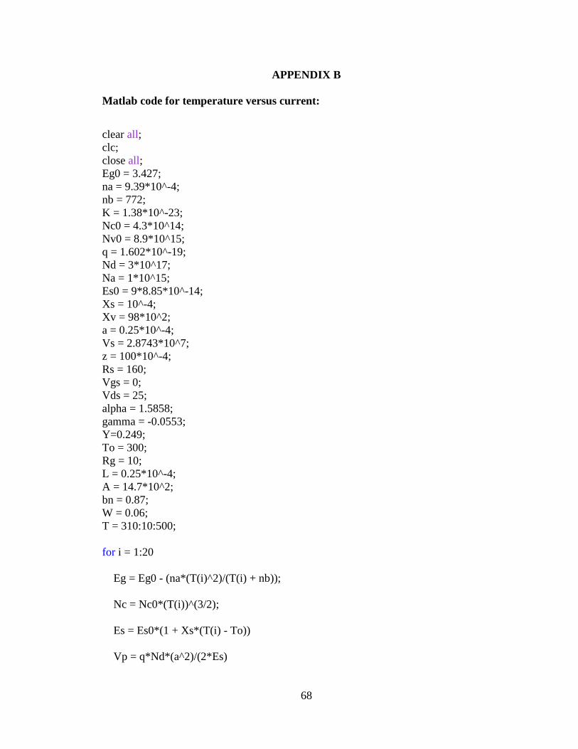
68
APPENDIX B
Matlab code for temperature versus current:
clear all;
clc;
close all;
Eg0 = 3.427;
na = 9.39*10^-4;
nb = 772;
K = 1.38*10^-23;
Nc0 = 4.3*10^14;
Nv0 = 8.9*10^15;
q = 1.602*10^-19;
Nd = 3*10^17;
Na = 1*10^15;
Es0 = 9*8.85*10^-14;
Xs = 10^-4;
Xv = 98*10^2;
a = 0.25*10^-4;
Vs = 2.8743*10^7;
z = 100*10^-4;
Rs = 160;
Vgs = 0;
Vds = 25;
alpha = 1.5858;
gamma = -0.0553;
Y=0.249;
To = 300;
Rg = 10;
L = 0.25*10^-4;
A = 14.7*10^2;
bn = 0.87;
W = 0.06;
T = 310:10:500;
for i = 1:20
Eg = Eg0 - (na*(T(i)^2)/(T(i) + nb));
Nc = Nc0*(T(i))^(3/2);
Es = Es0*(1 + Xs*(T(i) - To))
Vp = q*Nd*(a^2)/(2*Es)
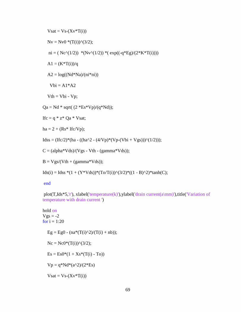
69
Vsat = Vs-(Xv*T(i))
Nv = Nv0 *(T(i))^(3/2);
ni = ( Nc^(1/2)) *(Nv^(1/2)) *( exp((-q*Eg)/(2*K*T(i))))
A1 = (K*T(i))/q
A2 = log((Nd*Na)/(ni*ni))
Vbi = A1*A2
Vth = Vbi - Vp;
Qa = Nd * sqrt( (2 *Es*Vp)/(q*Nd));
Ifc = q * z* Qa * Vsat;
ha = 2 + (Rs* Ifc/Vp);
Idss = (Ifc/2)*(ha - ((ha^2 - (4/Vp)*(Vp-(Vbi + Vgs)))^(1/2)));
C = (alpha*Vds)/(Vgs - Vth - (gamma*Vds));
B = Vgs/(Vth + (gamma*Vds));
Ids(i) = Idss *(1 + (Y*Vds))*(To/T(i))^(3/2)*((1 - B)^2)*tanh(C);
end
plot(T,Ids*5,'r'), xlabel('temperature(k)'),ylabel('drain current(a\mm)'),title('Variation of
temperature with drain current ')
hold on
Vgs = -2
for i = 1:20
Eg = Eg0 - (na*(T(i)^2)/(T(i) + nb));
Nc = Nc0*(T(i))^(3/2);
Es = Es0*(1 + Xs*(T(i) - To))
Vp = q*Nd*(a^2)/(2*Es)
Vsat = Vs-(Xv*T(i))
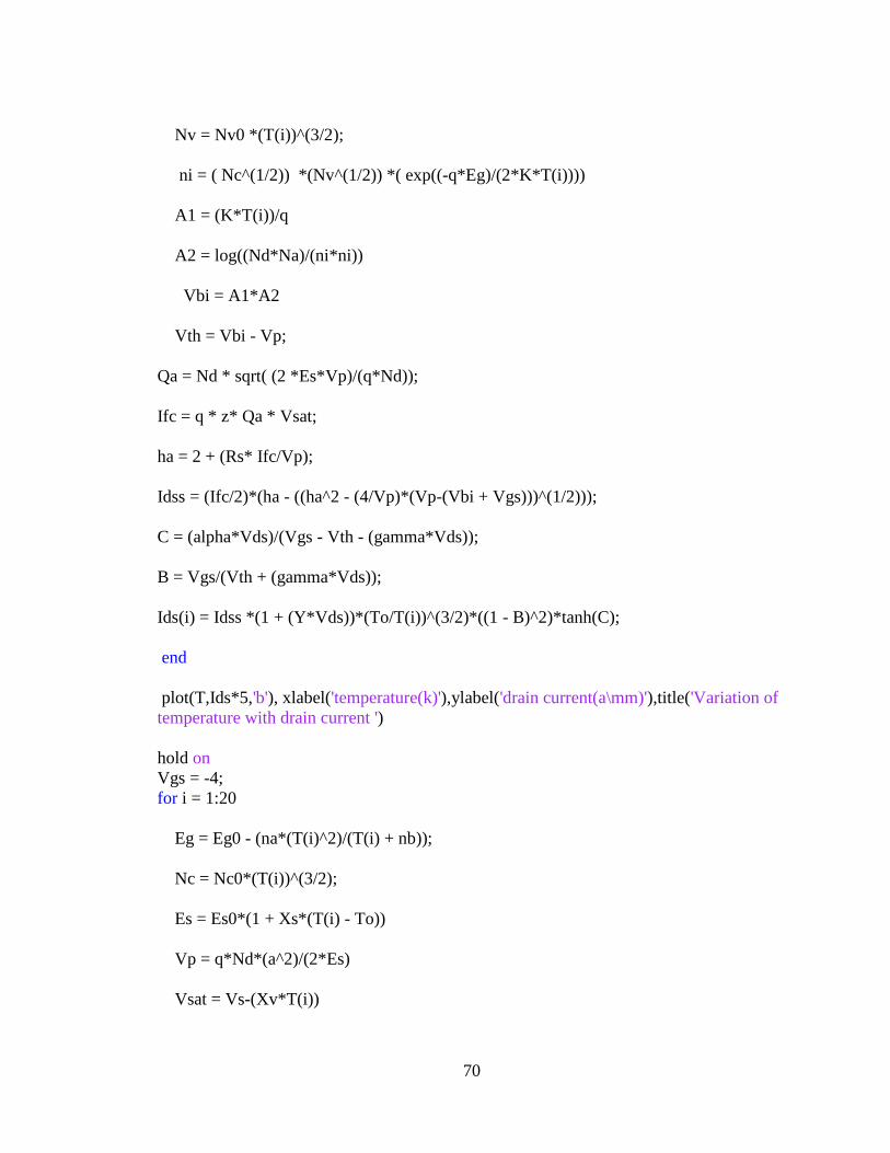
70
Nv = Nv0 *(T(i))^(3/2);
ni = ( Nc^(1/2)) *(Nv^(1/2)) *( exp((-q*Eg)/(2*K*T(i))))
A1 = (K*T(i))/q
A2 = log((Nd*Na)/(ni*ni))
Vbi = A1*A2
Vth = Vbi - Vp;
Qa = Nd * sqrt( (2 *Es*Vp)/(q*Nd));
Ifc = q * z* Qa * Vsat;
ha = 2 + (Rs* Ifc/Vp);
Idss = (Ifc/2)*(ha - ((ha^2 - (4/Vp)*(Vp-(Vbi + Vgs)))^(1/2)));
C = (alpha*Vds)/(Vgs - Vth - (gamma*Vds));
B = Vgs/(Vth + (gamma*Vds));
Ids(i) = Idss *(1 + (Y*Vds))*(To/T(i))^(3/2)*((1 - B)^2)*tanh(C);
end
plot(T,Ids*5,'b'), xlabel('temperature(k)'),ylabel('drain current(a\mm)'),title('Variation of
temperature with drain current ')
hold on
Vgs = -4;
for i = 1:20
Eg = Eg0 - (na*(T(i)^2)/(T(i) + nb));
Nc = Nc0*(T(i))^(3/2);
Es = Es0*(1 + Xs*(T(i) - To))
Vp = q*Nd*(a^2)/(2*Es)
Vsat = Vs-(Xv*T(i))

71
Nv = Nv0 *(T(i))^(3/2);
ni = ( Nc^(1/2)) *(Nv^(1/2)) *( exp((-q*Eg)/(2*K*T(i))))
A1 = (K*T(i))/q
A2 = log((Nd*Na)/(ni*ni))
Vbi = A1*A2
Vth = Vbi - Vp;
Qa = Nd * sqrt( (2 *Es*Vp)/(q*Nd));
Ifc = q * z* Qa * Vsat;
ha = 2 + (Rs* Ifc/Vp);
Idss = (Ifc/2)*(ha - ((ha^2 - (4/Vp)*(Vp-(Vbi + Vgs)))^(1/2)));
C = (alpha*Vds)/(Vgs - Vth - (gamma*Vds));
B = Vgs/(Vth + (gamma*Vds));
Ids(i) = Idss *(1 + (Y*Vds))*(To/T(i))^(3/2)*((1 - B)^2)*tanh(C);
end
plot(T,Ids*5,'g'), xlabel('temperature(k)'),ylabel('drain current(A)'),title('Variation of
temperature with drain current ')
hleg=legend ('Vgs=0v','Vgs=-2v','Vgs=-4v');
grid on

72
Matlab code current versus voltage for different Vgs: clear all;
clc;
close all;
Eg0 = 3.427;
na = 9.39*10^-4;
nb = 772;
K = 1.38*10^-23;
Nc0 = 4.3*10^14;
Nv0 = 8.9*10^15;
q = 1.602*10^-19;
Nd = 7*10^17;
Na = 1*10^15;
Es0 = 9*8.85*10^-14;
Xs = 10^(-4);
Xv = 98*10^2;
a = 0.25*10^-4;
Vs = 2.8743*10^7;
z = 100*10^-4;
Rs = 160;
alpha = 1.5858;
gamma = -0.0553;
Y=0.249;
To = 300;
T=300;
Eg = Eg0 - (na*(T^2)/(T + nb));
Nc = Nc0*(T)^(3/2);
Es = Es0*(1 + Xs*(T - To));
Vp = q*Nd*(a^2)/(2*Es);
Vsat = Vs-(Xv*T);
Nv = Nv0 *(T)^(3/2);
ni = sqrt ( Nc *Nv * exp((-q*Eg)/2*K*T));
Vbi = (K*T/q)*(log(Nd/ni)-log(Nc/Nd));
Vth = Vbi - Vp;
Qa = Nd * sqrt ( (2 *Es*Vp)/(q*Nd));
Ifc = q * z* Qa * Vsat;

73
ha = 2 + (Rs* Ifc/Vp);
Vgs = 0;
Idss = (Ifc/2)*(ha - ((ha^2 - (4/Vp)*(Vp-(Vbi + Vgs)))^(1/2)));
Vds = (0:1:100)
for i=10
C = (alpha*Vds)/(Vgs - Vth - (gamma*Vds(i)));
B = Vgs/(Vth + (gamma*Vds(i)));
Ids = Idss *(1 + (Y*Vds(i)))*(To/T)^(3/2)*((1 - B)^2)*tanh(C);
end
plot(Vds,Ids*5,'r'), xlabel('Drain to Source Voltage'),ylabel('Drain
Current'),title('Variation of temperature with drain current ')
hold on
Vgs = -2;
Idss = (Ifc/2)*(ha - ((ha^2 - (4/Vp)*(Vp-(Vbi + Vgs)))^(1/2)));
Vds = (0:1:100)
for i=10
C = (alpha*Vds)/(Vgs - Vth - (gamma*Vds(i)));
B = Vgs/(Vth + (gamma*Vds(i)));
Ids = Idss *(1 + (Y*Vds(i)))*(To/T)^(3/2)*((1 - B)^2)*tanh(C);
end
plot(Vds,Ids*5,'b'), xlabel('Drain to Source Voltage'),ylabel('Drain
Current'),title('Variation of temperature with drain current ')
hold on
Vgs = -4
;
Idss = (Ifc/2)*(ha - ((ha^2 - (4/Vp)*(Vp-(Vbi + Vgs)))^(1/2)));
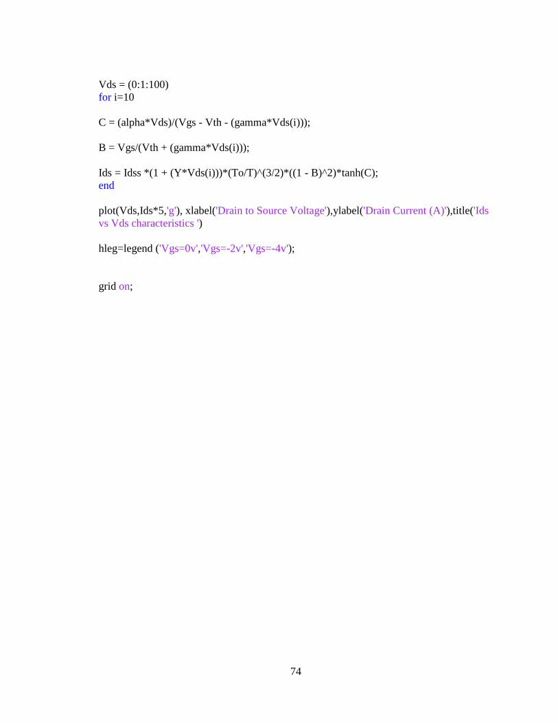
74
Vds = (0:1:100)
for i=10
C = (alpha*Vds)/(Vgs - Vth - (gamma*Vds(i)));
B = Vgs/(Vth + (gamma*Vds(i)));
Ids = Idss *(1 + (Y*Vds(i)))*(To/T)^(3/2)*((1 - B)^2)*tanh(C);
end
plot(Vds,Ids*5,'g'), xlabel('Drain to Source Voltage'),ylabel('Drain Current (A)'),title('Ids
vs Vds characteristics ')
hleg=legend ('Vgs=0v','Vgs=-2v','Vgs=-4v');
grid on;
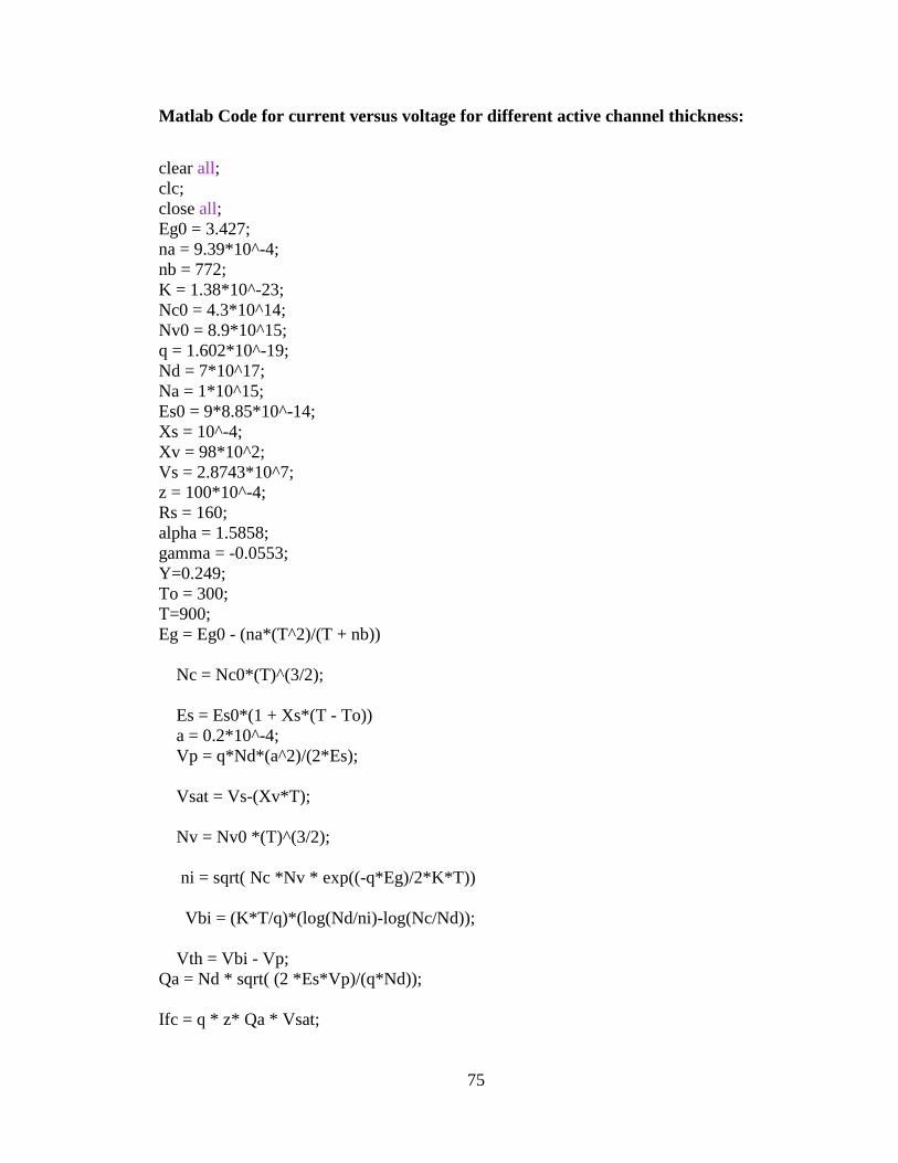
75
Matlab Code for current versus voltage for different active channel thickness:
clear all;
clc;
close all;
Eg0 = 3.427;
na = 9.39*10^-4;
nb = 772;
K = 1.38*10^-23;
Nc0 = 4.3*10^14;
Nv0 = 8.9*10^15;
q = 1.602*10^-19;
Nd = 7*10^17;
Na = 1*10^15;
Es0 = 9*8.85*10^-14;
Xs = 10^-4;
Xv = 98*10^2;
Vs = 2.8743*10^7;
z = 100*10^-4;
Rs = 160;
alpha = 1.5858;
gamma = -0.0553;
Y=0.249;
To = 300;
T=900;
Eg = Eg0 - (na*(T^2)/(T + nb))
Nc = Nc0*(T)^(3/2);
Es = Es0*(1 + Xs*(T - To))
a = 0.2*10^-4;
Vp = q*Nd*(a^2)/(2*Es);
Vsat = Vs-(Xv*T);
Nv = Nv0 *(T)^(3/2);
ni = sqrt( Nc *Nv * exp((-q*Eg)/2*K*T))
Vbi = (K*T/q)*(log(Nd/ni)-log(Nc/Nd));
Vth = Vbi - Vp;
Qa = Nd * sqrt( (2 *Es*Vp)/(q*Nd));
Ifc = q * z* Qa * Vsat;

76
ha = 2 + (Rs* Ifc/Vp);
Vgs = 0;
Idss = (Ifc/2)*(ha - ((ha^2 - (4/Vp)*(Vp-(Vbi + Vgs)))^(1/2)));
Vds = (0:1:100)
for i=10
C = (alpha*Vds)/(Vgs - Vth - (gamma*Vds(i)));
B = Vgs/(Vth + (gamma*Vds(i)));
Ids = Idss *(1 + (Y*Vds(i)))*(To/T)^(3/2)*((1 - B)^2)*tanh(C);
end
plot(Vds,Ids*5,'r'), xlabel('Drain to Source Voltage'),ylabel('Drain
Current'),title('Variation of temperature with drain current ')
hold on
a = 0.25*10^-4;
Vp = q*Nd*(a^2)/(2*Es);
Vsat = Vs-(Xv*T);
Nv = Nv0 *(T)^(3/2);
ni = sqrt( Nc *Nv * exp((-q*Eg)/2*K*T));
Vbi = (K*T/q)*(log(Nd/ni)-log(Nc/Nd));
Vth = Vbi - Vp;
Qa = Nd * sqrt( (2 *Es*Vp)/(q*Nd));
Ifc = q * z* Qa * Vsat;
ha = 2 + (Rs* Ifc/Vp);
Vgs = 0;
Idss = (Ifc/2)*(ha - ((ha^2 - (4/Vp)*(Vp-(Vbi + Vgs)))^(1/2)));
Vds = (0:1:100)
for i=10
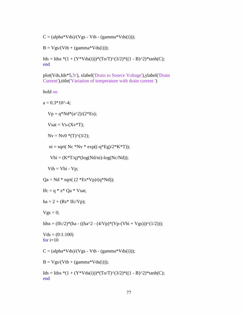
77
C = (alpha*Vds)/(Vgs - Vth - (gamma*Vds(i)));
B = Vgs/(Vth + (gamma*Vds(i)));
Ids = Idss *(1 + (Y*Vds(i)))*(To/T)^(3/2)*((1 - B)^2)*tanh(C);
end
plot(Vds,Ids*5,'b'), xlabel('Drain to Source Voltage'),ylabel('Drain
Current'),title('Variation of temperature with drain current ')
hold on
a = 0.3*10^-4;
Vp = q*Nd*(a^2)/(2*Es);
Vsat = Vs-(Xv*T);
Nv = Nv0 *(T)^(3/2);
ni = sqrt( Nc *Nv * exp((-q*Eg)/2*K*T));
Vbi = (K*T/q)*(log(Nd/ni)-log(Nc/Nd));
Vth = Vbi - Vp;
Qa = Nd * sqrt( (2 *Es*Vp)/(q*Nd));
Ifc = q * z* Qa * Vsat;
ha = 2 + (Rs* Ifc/Vp);
Vgs = 0;
Idss = (Ifc/2)*(ha - ((ha^2 - (4/Vp)*(Vp-(Vbi + Vgs)))^(1/2)));
Vds = (0:1:100)
for i=10
C = (alpha*Vds)/(Vgs - Vth - (gamma*Vds(i)));
B = Vgs/(Vth + (gamma*Vds(i)));
Ids = Idss *(1 + (Y*Vds(i)))*(To/T)^(3/2)*((1 - B)^2)*tanh(C);
end
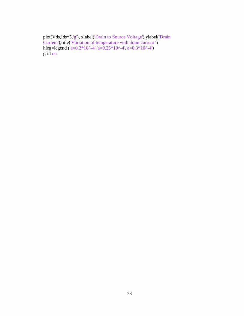
78
plot(Vds,Ids*5,'g'), xlabel('Drain to Source Voltage'),ylabel('Drain
Current'),title('Variation of temperature with drain current ')
hleg=legend ('a=0.2*10^-4','a=0.25*10^-4','a=0.3*10^-4')
grid on

79
Matlab code for transconductance versus temperature:
clear all;
clc;
close all;
Eg0 = 3.427;
na = 9.39*10^-4;
nb = 772;
K = 1.38*10^-23;
Nc0 = 4.3*10^14;
Nv0 = 8.9*10^15;
q = 1.602*10^-19;
Nd = 7*10^17;
Na = 1*10^15;
Es0 = 9*8.85*10^-14;
Xs = 10^-4;
Xv = 98*10^2;
a = 0.25*10^-4;
Vs = 2.8743*10^7;
z = 100*10^-4;
Rs = 160;
Vgs = -2;
alpha = 1.5858;
gamma = -0.0553;
Y=0.249;
To = 300;
Rg = 10;
L = 0.25*10^-4;
A = 14.7*10^2;
bn = 0.87;
W = 0.06;
T = 310:10:500;
for i = 1:20
Vds = 50;
Eg = Eg0 - (na*(T(i)^2)/(T(i) + nb));
Nc = Nc0*(T(i))^(3/2);
Es = Es0*(1 + Xs*(T(i) - To))
Vp = q*Nd*(a^2)/(2*Es)
Vsat = Vs-(Xv*T(i));
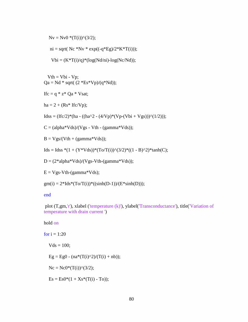
80
Nv = Nv0 *(T(i))^(3/2);
ni = sqrt( Nc *Nv * exp((-q*Eg)/2*K*T(i)));
Vbi = (K*T(i)/q)*(log(Nd/ni)-log(Nc/Nd));
Vth = Vbi - Vp;
Qa = Nd * sqrt( (2 *Es*Vp)/(q*Nd));
Ifc = q * z* Qa * Vsat;
ha = 2 + (Rs* Ifc/Vp);
Idss = (Ifc/2)*(ha - ((ha^2 - (4/Vp)*(Vp-(Vbi + Vgs)))^(1/2)));
C = (alpha*Vds)/(Vgs - Vth - (gamma*Vds));
B = Vgs/(Vth + (gamma*Vds));
Ids = Idss *(1 + (Y*Vds))*(To/T(i))^(3/2)*((1 - B)^2)*tanh(C);
D = (2*alpha*Vds)/(Vgs-Vth-(gamma*Vds));
E = Vgs-Vth-(gamma*Vds);
gm(i) = 2*Ids*(To/T(i))*((sinh(D-1))/(E*sinh(D)));
end
plot (T,gm,'r'), xlabel ('temperature (k)'), ylabel('Transconductance'), title('Variation of
temperature with drain current ')
hold on
for i = 1:20
Vds = 100;
Eg = Eg0 - (na*(T(i)^2)/(T(i) + nb));
Nc = Nc0*(T(i))^(3/2);
Es = Es0*(1 + Xs*(T(i) - To));
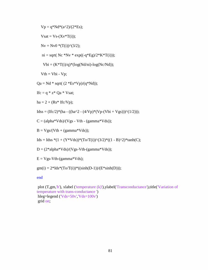
81
Vp = q*Nd*(a^2)/(2*Es);
Vsat = Vs-(Xv*T(i));
Nv = Nv0 *(T(i))^(3/2);
ni = sqrt( Nc *Nv * exp((-q*Eg)/2*K*T(i)));
Vbi = (K*T(i)/q)*(log(Nd/ni)-log(Nc/Nd));
Vth = Vbi - Vp;
Qa = Nd * sqrt( (2 *Es*Vp)/(q*Nd));
Ifc = q * z* Qa * Vsat;
ha = 2 + (Rs* Ifc/Vp);
Idss = (Ifc/2)*(ha - ((ha^2 - (4/Vp)*(Vp-(Vbi + Vgs)))^(1/2)));
C = (alpha*Vds)/(Vgs - Vth - (gamma*Vds));
B = Vgs/(Vth + (gamma*Vds));
Ids = Idss *(1 + (Y*Vds))*(To/T(i))^(3/2)*((1 - B)^2)*tanh(C);
D = (2*alpha*Vds)/(Vgs-Vth-(gamma*Vds));
E = Vgs-Vth-(gamma*Vds);
gm(i) = 2*Ids*(To/T(i))*((sinh(D-1))/(E*sinh(D)));
end
plot (T,gm,'b'), xlabel ('temperature (k)'),ylabel('Transconductance'),title('Variation of
temperature with trans-conductance ')
hleg=legend ('Vds=50v','Vds=100v')
grid on;