capacity model with sustainability scope to …
TRANSCRIPT

CAPACITY MODEL WITH SUSTAINABILITY SCOPE TO PREDICT THE
SEMICONDUCTOR MANUFACTURING’S ENERGY CONSUMPTION AND
CARBON DIOXIDE EMISSIONS
by
Thulasi Krishna Kannaian B.S.
A thesis submitted to the Graduate Council of
Texas State University in partial fulfillment
of the requirements for the degree of
Master of Science with a
Major in Engineering
December 2018
Committee Members:
Jesus A. Jimenez, Chair
Cecilia Temponi, Co-Chair
Tongdan Jin

COPYRIGHT
by
Thulasi Krishna Kannaian
2018

FAIR USE AND AUTHOR’S PERMISSION STATEMENT
Fair Use
This work is protected by the Copyright Laws of the United States (Public Law 94-553,
section 107). Consistent with fair use as defined in the Copyright Laws, brief quotations
from this material are allowed with proper acknowledgment. Use of this material for
financial gain without the author’s express written permission is not allowed.
Duplication Permission
As the copyright holder of this work I, Thulasi Krishna Kannaian, authorize duplication
of this work, in whole or in part, for educational or scholarly purposes only.
.

DEDICATION
I would like to dedicate this thesis to my family for all the guidance,
encouragement and support throughout my life. I also dedicate this report to my friends
for their constant help and support.

v
ACKNOWLEDGEMENTS
I would like to express my gratitude to all who helped me during the wring
of this thesis at Texas State University.
First, I would like to express my deep gratitude to Dr. Jesus A. Jimenez, my
Supervisor, for his continuous support and encouragement, for his patience, motivation,
enthusiasm, and immense knowledge. He also provides me with an excellent atmosphere
for conducting this research project. Without his consistent and illuminating instruction,
this thesis could not have reached its present form.
I would also like to express my heartfelt gratitude to my thesis committee members:
Dr. Cecilia Temponi and Dr. Tongdan Jin for their insightful comments and constructive
suggestions in the early version of the work.
I owe a special debt of gratitude to Dr. Vishu Viswanthan, Graduate Advisor of
Engineering, and Dr. Stan McClellan, former Director of Ingram School of Engineering,
for providing facility support. I would also like to thank Dr. Patrick L. Thomas and Ms.
Sarah Pierce in Ingram School of Engineering for their kind help.
Finally, I express my gratitude to my parents, family and friends for providing me with
unfailing support and continuous encouragement throughout my years of study and through
the process of researching and writing this thesis. This accomplishment would not have
been possible without them.

vi
TABLE OF CONTENTS
Page
ACKNOWLEDGEMENTS..................................................................................... v
LIST OF TABLES .................................................................................................. ix
LIST OF FIGURES ................................................................................................. x
LIST OF ABBREVATIONS .................................................................................. xi
ABSTRACT ......................................................................................................... xiii
CHAPTER
1. INTRODUCTION ...................................................................................... 1
1.1 Problem Description ............................................................................. 1
1.2 Research Objective ............................................................................... 4
1.3 Thesis Outline ....................................................................................... 5
2. LITERATURE REVIEW ........................................................................... 6
2.1 Semiconductor Manufacturing............................................................. 6
2.2 Electricity Consumption ...................................................................... 7
2.3 Factors Affecting Energy Consumption in Wafer Fab ...................... 10
2.4 Simulation Models with Renewable Energy Integration ................... 12
2.5 Carbon Emission and Carbon Tax ..................................................... 15
2.6 Production Planning of the Supply Chain Model .............................. 21
2.7 Modeling Sustainability for Production Planning.............................. 24

vii
3. METHODOLOGY ................................................................................... 30
3.1 List of Variables and Parameters ....................................................... 31
3.2 Capacity Performance Measures........................................................ 32
3.3 Electricity Consumption Metrics ....................................................... 33
3.4 Comparison of PEI and EUI .............................................................. 34
3.5 Capacity Model for Electrical Power Consumption Estimation using
WIP Lot Data (kWh-WIP) ................................................................. 35
3.6 Capacity Model for Electrical Power Consumption Estimation using
Tool-level Utilization (kWh-Tool) .................................................... 36
3.7 Carbon Dioxide Emission Calculation............................................... 38
3.8 Description of Simulation Model....................................................... 38
3.9 Selection of Optimal PEI value.......................................................... 43
3.10 Simulation Process ........................................................................... 43
4. RESULTS AND DISCUSSION .............................................................. 47
4.1 Design of Experiments ....................................................................... 47
4.2 Design of Simulation Experiment ...................................................... 49
4.3 Results for the kWh-WIP ................................................................... 50
4.4 Results for the kWh-Tool................................................................... 54
4.5 Comparisons between kWh-WIP vs. kWh-Tool ............................... 55
4.6 Error % ............................................................................................... 58
4.7 Insights of kWh-WIP ......................................................................... 59
4.8 Insights of kWh-Tool ......................................................................... 59

viii
4.9 EUI Comparison ................................................................................ 60
4.10 Bottleneck Station Utilization Study ............................................... 61
4.11 CO2 Emission Calculation ............................................................... 63
5. CONCLUSION AND FUTURE WORK ................................................. 66
5.1 Conclusion ......................................................................................... 66
5.2 Managerial Decision Making and Impact .......................................... 67
5.2 Future Work ....................................................................................... 68
APPENDIX SECTION ................................................................................ 70
REFERENCES ............................................................................................. 88

ix
LIST OF TABLES
Table Page
1. Station Family –Process Mapping ................................................................... 40
2. Wafer Fab Production and Energy Indices ...................................................... 43
3. Fab Profile Definition ...................................................................................... 48
4. Repeats Calculation for Each Scenario or Fab Type ....................................... 49
5. Power Consumption Calculation for the kWh-WIP method ........................... 52
6. PEI Analysis for the kWh-WIP method .......................................................... 53
7. EUI Analysis for the kWh-WIP method ......................................................... 53
8. Fab Profile Comparison ................................................................................... 56
9. Annual Power Consumption values for kWh-WIP and kWh-Tool ................. 57
10. Annual Power Consumption Error% between kWh-WIP and kWh-Tool ...... 58
11. Bottleneck Station-Process and Utilization percentage for each fab type ....... 61
12. Carbon Dioxide Calculation for Fabs based on kWh-WIP ............................. 64

x
LIST OF FIGURES
Figure Page
1. Global Semiconductor Sales from 1987 to 2017 ............................................... 1
2. Semiconductor Manufacturing .......................................................................... 6
3. Power Consumption of Semiconductor Fabrication Plant ................................ 9
4. A Grid-Connected Solar PV System and Wind Turbine System .................... 15
5. Inputs and Outputs for the MIMAC Model..................................................... 39
6. Number of tools in each process ..................................................................... 41
7. Fab Electricity Consumption ........................................................................... 42
8. Simulation Process .......................................................................................... 46
9. WIP lots recorded across scenario runs for every fab type ............................. 50
10. Annual Power Consumption for kWh-WIP and kWh-Tool ............................ 57
11. kWh-WIP EUI vs. kWh-Tool EUI comparison .............................................. 60
12. Bottleneck Station Utilization for each fab type ............................................. 62
13. Carbon Emissions per year visualization for the different fab types .............. 64
14. Methodologies and Anticipated Interactions in this study .............................. 69

xi
LIST OF ABBREVIATIONS
Abbreviation Description
IC Integrated Circuits
PC Personal Computer
WSTS World Semiconductor Trade Statistics
GHG Green House Gas
DG Distributed Generation
WT Wind Turbines
PV Solar Photovoltaic
OR Operation Research
WIP Work-in-Process
ITRS International Technology Roadmap for
Semiconductors
DRAM Dynamic Random-Access Memory
EUI Electrical Utilization Index
PEI Production Efficiency Index
UOP Units of Production
HVAC Heating, Ventilation, and Air Conditioning
EOQ Economic Order Quantity
PFC Perfluorocarbons
AMHS Automated Material Handling Systems
CT Cycle Time
TH Throughput
LP Linear Programming
BOM Bills of Materials
TI Texas Instruments
UPW Ultra-Pure Water

xii
PCW Process Cooling Water
MEMS Micro-Electro-Mechanical Systems
RF chips Radio Frequency Chips
CMP Chemical Mechanical Polishing
ECP Electro Chemical Plating
WLSPY Wafer Lots Starts Per Year
WSPY Wafer Starts Per Year
MTTR Mean Time To Repair
MTBF Mean Time Before Failure
MIMAC Measurement and Improvement of Manufacturing
Capacity
DOE Design of Experiments
PFC Perfluorinated Carbon
RT Refrigeration Ton
xiii
ABSTRACT
Semiconductor industries are not only technology-intensive, but also highly
energy-intensive. A wafer fab consumes about 300-400 kWh/day. To supply this amount
of electricity, the amount of carbon dioxide released is approximately 180–360 metric tons
per day. This emission causes climate change and also rise in energy costs. Thus, it is
important to take measures to reduce energy consumption.
The scientific merit of this research is to develop two methods designed to estimate
the electric energy consumption and production of a semiconductor wafer fab. The broader
impact of the research is that the methods can be extended to other manufacturing
industries, even though they are framed in this study in the context of the semiconductor
manufacturing industry. The first method, referred to as kWh-WIP, is capacity model that
estimates electricity consumption by using WIP lot information. The second method
referred here as kWh-Tool is a capacity model that estimates electricity consumption by
using tool-level utilization. A relation is established between the two levels of detail models
by comparing them with respect to annual electricity consumption and carbon emissions.
Power consumption of tools and tool-process mapping are obtained by intensive research
and surveying with the professionals from the semiconductor manufacturing industry. The
Measurement and Improvement of Manufacturing Capacity data set is used as the basis for
the capacity simulations of this thesis work. The dataset represents 200mm wafer fab
processes. The average Electrical Utilization Index (EUI) and Production Efficiency Index
(PEI) computed with kWh-Tool methodology across all nine 200 mm fab considered in

xiv
this study was 0.145kWh/UOP and 1.987 kWh/cm2 respectively. The average annual
power consumption is 44,745,707 kWh. Annual Power Consumption values calculated in
kWh-WIP and kWh-Tool methodologies are closer with a variation of less than 3%. The
PEI values for different fab type computed from the kWh-Tool methodology is similar to
the Optimal theoretical value of 1.231 (kWh/cm2).

1
1. INTRODUCTION
1.1 Problem Description
Semiconductors are an essential part of many commonly used electronic devices,
such as PCs, mobile phones, radios, tablets, and many more. Semiconductor manufacturing
deals with producing integrated circuits (ICs) on silicon wafers, thin discs made from
silicon and gallium arsenide. The semiconductor industry is a vast and highly competitive
industry. The industry is characterized by large fluctuations in product supply and demand,
depending heavily on the strength of the global economy. Worldwide semiconductor sales
reached $408.69 billion in 2017 according to the figures from World Semiconductor Trade
Statistics (WSTS) [1].
Figure 1 Global Semiconductor Sales from 1987 to 2017 [1]

2
Figure 1 shows the global semiconductor industry sales each year. The
Semiconductor Industry Association reports that the global semiconductor industry sales
reached $412 billion in 2017, which is an increase of 21.6% compared to the previous year.
2017 had the industry’s highest-ever annual sales. Intel is the largest semiconductor chip
manufacturer with revenues of 54 billion U.S. dollars in 2016 [1].
ICs are manufactured through a series of steps namely wafer fabrication, sort,
assembly, and final test. The wafer fabrication part of the overall manufacturing process is
carried out in semiconductor wafer fabrication facilities (wafer fabs). In this process,
electronic circuits are built layer-by-layer onto the wafers – a process that might take a total
processing time of several weeks depending on the product complexity. Wafer fabrication
can be produced with in-house facilities or may be outsourced to subcontractors. Once they
are processed in the wafer fab, wafers are sorted for any defects using electrical tests, after
which the probed wafers are transferred to assembly facilities where dices of appropriate
quality are packaged. These again are sent for testing to ensure that only high-quality
products are delivered to the customers. Wafer fab and sorting are often referred to as the
front-end, while assembly and test are called the back-end. All these processes utilize a
large amount of electricity, particularly those done at the wafer fab.
A modern wafer fabrication facility consumes about 300-400 kWh/day on average,
which can power approximately around 10,000 homes per day. Wafer fabrication processes
are highly energy-intensive with annual energy utility bills of up to $10–20 million for a
single wafer fab [2]. To supply this amount of electricity, the amount of carbon dioxide
released by fossil fuel-fired power plants is estimated to be 180–360 metric tons per day.
This estimation is made based on the factor that 0.6–0.9 Kg CO2 is released when 1 kWh
3
electricity is produced from a fossil fuel-fired power plant [3]. Climate change is a
universally recognized 21st-century global environmental challenge. The impact of energy
consumption on climate change and the rising cost of energy has become an extremely
important issue faced by the semiconductor manufacturing industry today. Thus, chip
manufacturers are increasingly driving efforts to reduce greenhouse gas emissions of their
manufacturing facilities.
Energy efficiency has not been the high priority for management concern because
energy costs were about 1-2 percent of total production costs, including buildings,
capitalized land and equipment. This traditional way of viewing the fab’s electricity
consumption is now changing [2]. It is important to evaluate energy consumption in a
semiconductor wafer fab because electricity is becoming one of the most expensive
operational expenses. Energy costs can account for 5-30% of fab operating expenses,
depending on the electricity prices. 30-40% percent of the fab’s electricity consumption is
from the wafer processing tools, whereas 50% of this consumption is due to the sub-fab
systems, such as the air conditioning units, cleanroom heating, and ventilation [2].
Capacity planning involves determining the various facilities’ resources required,
with the focus in computing the number of tools that are required to maximize throughput
(TH) with minimal work-in-process (WIP) and cycle time (CT). Jimenez et al. (2008) [4]
reported several approaches for conducting capacity analysis for semiconductor
manufacturing. These papers lack modeling components to enable the study of
sustainability issues, such as carbon emissions and electricity consumption. Many papers
with several mathematical models on environmental references and standards are available,
but these models are unable to estimate electricity consumption. Estimation of energy

4
consumption is very important in order to reduce the CO2 emissions by burning fossil fuels.
This helps in reducing global warming. The cost of energy consumption can be reduced by
incorporating renewable energy constraints into the capacity planning model. This also
reduces the carbon dioxide emission and helps us to achieve sustainability. Renewable
technology in the distributed generation system is quite appealing because they harness
renewable sources for energy production, resulting in zero carbon emission.
1.2 Research Objective
This research proposes two capacity modeling methods to estimate electricity
consumption and carbon dioxide emissions using key performance indicators, such as WIP,
CT, and TH. The first method, called kWh-WIP, represents a capacity model for power
consumption estimation using WIP lot data. The second method, called kWh-Tool,
represents a capacity model for power consumption estimation using tool-level utilization
data.
The research objectives are as follows:
1. To describe two simulation modeling methods that estimates annual electricity
consumption and carbon dioxide emissions for a semiconductor wafer fab.
2. To compare the predictive accuracy of the simulation modeling methods performing
under different scenarios varying the wafer starts per year and product mix levels.
3. To propose modeling guidelines and identify the obstacles of simulating the capacity
model for predicting the fab’s electricity consumption.

5
1.3 Thesis Outline
This thesis is organized as follows: Chapter 2 provides a detailed literature review
based on previous work done in capacity modeling for production planning and capacity
analysis in semiconductor manufacturing, with a focus on sustainability. Chapter 3 explains
the methodology and describes the designed simulation model. Chapter 4 presents the
designed simulation experiments and discusses the simulation results. Chapter 5 concludes
this research and discusses future work.

6
2. LITERATURE REVIEW
2.1 Semiconductor Manufacturing
Semiconductor manufacturing consists of front-end operations, where the surface
of raw silicon wafers is modified to create a pattern of integrated circuits, and of back-end
operations, where wafers are cut into individual microchips (dies), put in a package, and
tested. It has become standard to term the fabrication and sort phases as the “front-end”
and final test phases being called the “back-end.”
Figure 2 Semiconductor Manufacturing [5]
The mass production of integrated circuits (ICs) can be divided into four different
phases: fabrication, sort (probe), assembly, and final test [6]. Figure 2 displays an example
of a semiconductor supply chain network. Fabrication is the process of transforming a pure
silicon (or gallium arsenide) wafer into a wafer with completed ICs. This process requires
300 to 700 different process steps; this is the most complex portion of the entire process.
The formation of one layer of the wafer can include cleaning, oxidation/diffusion, film
deposition, photolithography, planarization, etching, ion implantation, and inspection;
there may be up to 40 layers per wafer to build the completed ICs. Additionally, re-entrant
flows exist, as the equipment used for these steps are expensive; the same wafer may be
processed on the same machine multiple times (and competes for the machine’s capacity
with other wafers being produced) [7].

7
After a wafer completes fabrication, it proceeds to the sort (or probe) phase. The
individual ICs on each wafer are tested for basic functionality. An electronic map is
generated for each wafer, indicating those ICs on the wafer that failed. As in the fabrication
phase, there is uncertainty in the number of ICs that survive sort. After sort is complete,
wafers go to die bank (i.e., the completed wafer WIP) where they wait for the assembly
and final test phases.
In the assembly phase, the wafer is cut into individual ICs or known as dies, and
the failed ICs are discarded (scrapped). Functional ICs are then packaged wherein
connections are made between the chip and the lead frame, and then the whole circuit is
encapsulated for protection. The packaged ICs then move to the final test phase. At this
point, the ICs are tested, rated (binned), and ultimately date-stamped for inclusion in
finished goods inventory. These last two phases are still complex, but not to the extent of
the first two; assembly and final test deal with millions of devices versus the thousands of
wafers handled in fabrication and sort.
2.2 Electricity Consumption
Semiconductor manufacturing facilities, also known as wafer fabs, consume a large
amount of electricity in daily operation as discussed above. The semiconductor
manufacturing industry is confronted with two major facility challenges like many other
industries, i.e., energy conservation and reduction of greenhouse gas emissions. ITRS has
set aggressive goals for the industry about energy conservation in the next 10–20 years.
More specifically, the wafer fab’s energy consumption is expected to decrease from the
current 1.9 kWh/cm2 to 1.2 kWh/cm2 by 2016 [8]. ITRS plans to achieve the goal by

8
implementing sustainable facilities and deploying green and cost-effective manufacturing
processes.
Current approaches to sustainable manufacturing processes usually focus on energy
conservation by improving equipment or tool efficiency. Although energy conservation is
an effective method to improve the performance of wafer fabs, the following concerns are
expressed by ITRS [2]:
1) The increase in the wafer size from 300 to 450 mm requires more energy per wafer;
2) The industry will potentially build new facilities or expand existing capacities to meet
the market demand; and
3) The fabs carbon dioxide footprint from conventional power plants is difficult to
quantify, and the criteria for controlling emission need to be defined.
Wafer fabs are highly energy-intensive and it consumes about 300–400 MWh per
day [8], and 15-30 MW of daily load. This can power up to 10,000 homes in the U.S. In
order to supply this amount of electricity, power plants are used but this emits 180–360
metric tons of carbon dioxide per day [3]. This value is calculated by assuming 0.6–0.9 Kg
CO2 released when 1 kWh electricity is produced [3]. A wafer fab typically contains
hundreds of highly automated processing tools along with dozens of utility support
systems, such as chillers, recirculating air fans, nitrogen plants, and exhaust air systems.
The overall utility bill ranges from $12-$25 million. The three major factors dominating
energy consumption in wafer fabs results are highlighted below [2]:
40% of energy is used to power the processing tools.
57% of energy powers the cleanrooms and recirculation air fans.

9
The remaining energy is used to supply ultra-pure water and pure gases to certain
manufacturing processes.
Figure 3 Power Consumption of Semiconductor Fabrication Plant [2]
Power Manufacturing
Equipment, 44%
Utilities Manufacturing
Equipment, 40%
Infrastructure, 17%
Power consumption of semiconductor fabrication plant

10
2.3 Factors Affecting Energy Consumption in Wafer Fab
Hua et al. (2007) presented the factors affecting energy conservation in the wafer
fab. Semiconductor wafer fab consumes a tremendous amount of electricity. Most fabs
have cooling capacities over 10,000 RT (Refrigeration Tons), which is much larger than
common commercial buildings. The energy allocation of the facility systems in a fab is
affected by the following factors [9]:
a. Fans consume high power to re-circulate filtered airflow in order to maintain a clean
environment.
b. Significant power is required to maintain stable cleanroom temperature and humidity
(e.g., 24 ± 0.5 8oC and 40 ± 5%RH).
c. Heat produced by the manufacturing process tools increases the load of the cooling
system.
d. Pumps and compressors consume significant electricity to produce ultra-pure water
(UPW) and gases.
e. Treatment and processing of exhaust air require significant power. Energy is also used
to pre-treat large volumes of outside air to compensate for the exhaust air in order to
keep the cleanroom under positive pressure.
So, benchmarking is an important step in implementing energy conservation in a
semiconductor fab. A semiconductor cleanroom facility system is complicated, usually
comprised of several sub-systems, such as a chilled water system, a make-up system, an
exhaust air system, a compressed air system, a process cooling water (PCW) system, a
nitrogen system, a vacuum system, and an ultra-pure water (UPW) system. It is a daunting
task to allocate energy consumption and determine an optimum benchmark.
11
Hu et al. (2010) researched on characterizing the energy use in 300mm DRAM
(Dynamic Random-Access Memory) wafer fabrication plants in Taiwan by performing
surveys and on-site measurements. The objective of this paper is to characterize the electric
energy consumption and production of 300mm DRAM fabs by using various performance
metrics. These performance metrics include the EUI (Electrical Utilization Index) and PEI
(Production Efficiency Index). The results show that the EUI and PEI values are 0.0272
kWh/UOP and 0.743 kWh/cm2, respectively. Using EUI in assessing the energy efficiency
of the fab production provides more consistent comparisons than just using PEI [10].
Many of the actions undertaken to improve the energy efficiency of a
manufacturing company are aimed at getting energy-consuming devices to operate more
efficiently or at conserving energy within a plant. Such actions could include optimizing
boiler efficiency, installing energy-efficient equipment, retrofitting fixed-speed motors
with variable speed drives, or improving insulation in plant and buildings. While these
device-oriented energy efficiency measures can achieve considerable savings, greater
energy savings may be achieved in many instances by improving the efficiency of
manufacturing processes.
The simplest and most valuable measure of energy efficiency achievements in a
manufacturing plant is unit consumption or energy used per unit produced. Unit
consumption provides the best indicator of how effectively the energy consumed by a plant
is being used and can be tracked over time to measure energy efficiency improvements. If
we define energy used per unit produced as a measure of energy efficiency in a
manufacturing plant, then there are two complementary approaches to increase the energy
efficiency of a plant: reducing energy consumption and increasing productivity. Factors

12
that reduce the productivity of a plant also reduce its energy efficiency. The greatest source
of energy waste in any manufacturing plant could be an inefficient manufacturing process,
a poorly planned production schedule, or poor product quality. An energy management
policy that focuses only on improving the energy efficiency of energy-consuming devices
or on energy conservation will not recognize or address these problems and will, therefore,
have limited success. An effective energy management system should also incorporate
energy-saving opportunities that can be realized by improving the overall production
efficiency of a plant [11].
The cost of energy consumption can be reduced by incorporating renewable energy
constraints into the capacity planning model. This also reduces the carbon dioxide
emissions and helps us to achieve sustainability. Renewable technology like wind and solar
generation system is quite appealing because they harness renewable sources for energy
production, resulting in zero carbon emission.
2.4 Simulation Models with Renewable Energy Integration
Long-term environmental sustainability can be achieved by incorporating
renewable energy in the semiconductor wafer fab. Recently distributed generation (DG)
emerged as a new system for energy production and consumption. DG units are installed
in the consumer site where large electricity is needed. This technology is also an integral
part of the smart grid with the goal of reducing the greenhouse gas emissions by adapting
onsite renewable power generation. It includes wind turbines (WT), solar photovoltaics
(PV), micro-turbines, diesel engines and fuel cells of which the capacity is usually less than
10 MW [3]. The advantages of using DG technology are:

13
Since DG systems are installed on the site, it reduces the transmission bottleneck.
There is no carbon emission.
It refines the electricity supply reliability.
Cost reduction in the utility bills.
Santana-Viera et al. (2015) proposed a distributed generation (DG) system
comprising WT and solar PV units to power the wafer fab along with the main grid. The
major challenge in deploying renewable DG technology is the power volatility. To design
a robust DG system, both the power volatility and the load uncertainty must be
appropriately quantified and incorporated into the design model. The purpose of the DG
planning is to determine the generator type, capacity, and placement such that the overall
system cost is minimized, or the energy yield is maximized [12].
The main obstacle to deploying wind and solar-based DG technologies is the high
installation cost coupled with the intermittent power. Therefore, to reliably operate a
renewable DG system, both the power intermittency and the payback period must be
appropriately analyzed and incorporated into planning models. Several manufacturing and
service industries have adopted onsite renewable energy to power their facilities along with
the main grid. There is a lack of research activities targeting the modeling and
implementation of wind–solar-based DG systems in a large manufacturing or public
service settings.
Many papers leverage probability theories and analytics tools to model the random
power generation and to optimize the capacity of onsite renewable DG systems. These
papers, optimization models are formulated to determine the capacity of WT and PV units

14
such that the anticipated cost savings are maximized by considering the stochastic nature
of wind speed and weather conditions.
A significant amount of electricity is required to support the operation of any large
manufacturing facilities. Semiconductor manufacturing facilities, also known as wafer
fabs, consume an enormous amount of electricity in daily operation. Integrating renewable
energy into the wafer fabs alleviates the greenhouse gas emissions, reduces the utility bills
and improves the energy security. A grid-connected DG system comprising of wind
turbines, solar photovoltaics, a net metering module, and a substation is used. A
quantitative approach is developed to guide the wafer fab to choose the energy technology
and the generation capacity, aiming to minimize the system cost while mitigating the
carbon footprint.
Villarreal et al. (2013) proposed the integration of renewable energy into the
modern semiconductor industry. This paper presents a stochastic programming model to
aid the planning and operation of distributed generation system in the presence of power
volatility and load uncertainty. The proposed distributed generation (DG) system
comprises WT and solar PV units to power the wafer fab along with the main grid [2].
Ziarnetzky et al. (2017) developed a model considering the elements of a
sustainable and distributed generation system into a mid-term production planning
formulation for a wafer fab. The major daily energy supply of the wafer fab is from the
WTs and solar PVs. The surplus energy is returned to the main grid. Production-related
costs, the cost for energy from the substation, and penalty costs when there is a lack of the
renewable energy penetration were considered, and they could be reduced by offering
renewable surplus energy to the main grid. A simulated environment was created to run

15
the obtained production plans to compute the expected profit in the face of machine
breakdowns, wind power volatility, and uncertain power output of the solar PVs. This
approach helps to determine an appropriate number of WTs and solar PVs for a given
demand scenario. The results showed that it is reasonable to combine production-related
planning and decisions with respect to the design of a DG system [6].
Figure 4 A Grid-Connected Solar PV and Wind Turbine System [5]
2.5 Carbon Emission and Carbon Tax
A carbon tax is defined as a fee imposed on greenhouse gas emissions generated by
burning fuels. This tax puts a price on each ton of GHG emitted; this results in a powerful
market response across the entire economy reducing emissions. These taxes can be a
retrogressive tax; this may affect the low-income groups disproportionately directly or
indirectly. Several countries have imposed carbon taxes or energy taxes. By increasing fuel
efficiency, reducing fuel consumption, businesses and individuals, using cleaner fuels and
adopting new technology can reduce the amount paid on the carbon tax [13].
In recent years, the global green tax landscape is evolving rapidly and becoming
more complex, as governments widely use taxation as a tool to achieve green policy goals

16
and make firms operate more sustainably. A number of pollution taxes are levied, and
subsidies are offered around the world. In September 2012, the Japanese government
introduced a new tax to curb greenhouse gas emissions [13]. France foisted a general tax
for polluting activities names as “pay as you pollute.” In the US, there are a large number
of sub-national state-based tax incentives related to pollution control and ecosystem
protection [13]. The carbon tax provides economic and social benefits. It aims to reduce
the harmful and unfavorable emissions of CO2 in the atmosphere, thus slowing down
climate change and its negative effects on the human health and environment. It is a cost-
effective method of reducing the GHG (Green House Gases) emissions.
Strand et al. (2015) analyzed the policy bloc of fossil fuel importers that prefers the
tax to the cap. It executes an optimal climate policy, faces a fringe of other fuel importers
and an exporter bloc. It purchases offset from the (non-policy) fringe. Since the tax reduces
the price of fuel export and buys more when the policy bloc is larger, offsets are more
favorable to the policy bloc under a tax when compared to the cap [14].
By taking into consideration the operational costs and social costs Hung et al.
(2014) proposed a strategic decision-making model. These costs are caused by the CO2
emission from a SCM for SSCM. Under different scenarios, the operational costs and
carbon dioxide emissions were evaluated in the manufacturing SCM. The results showed
that the amount of carbon dioxide emission came down with increasing social cost rate of
carbon dioxide emissions. Lastly, it is concluded that the effective approach to reducing
carbon dioxide emissions is to force the enterprises to bear the costs of carbon emissions
resulting from their economic activities [15].
Jin et al. (2014) investigated on carbon emission tax, inflexible cap, and cap-and-

17
trade. Redesign of the supply chains and choices of transportation (truck, rail, or waterway)
may influence a company. This paper mainly focuses on the optimization of the models for
major retailers, who make a huge contribution to freight movement, to design their supply
chains under various carbon policies. The policymakers can predict the impact of policies
on overall emissions in the freight transportation sector using the results. The model, when
incorporated into the integrated assessment models, can be effective in climate change
analyses. Besides the impact of the policy parameters on carbon emissions and logistics
cost is studied using a sensitivity analysis [16].
Du et al. (2009) emphasized on the influence of emission cap-and-trade mechanism
in an emission-dependent supply chain. The emission dependent supply chain comprises
of the emission permit supplier and the emission-dependent firm. Emission cap/quota
imposed by the government and permits purchased via emission trading were taken into
focus. Extra permits need to be purchased if the quota is inadequate to satisfy the target
production. The unique Nash equilibrium derivation is presented, and a game-theoretical
analytical model is proposed in this paper. Optimal decisions are made by the emission
permit supplier on permit pricing and the emission-dependent firm on production quantity.
The paper concludes that the governmental environment policy, several exogenous factors,
the market risk, etc. affect the players' bargaining power [17].
Based on the economic order quantity (EOQ) model, Bian et al. (2015) examined
the production lot sizing issues of a firm under two regulations, i.e., cap-and-trade and the
carbon tax. This paper investigates the impacts of production and regulation parameters on
the optimal lot size and emissions. It shows that under the cap-and-trade regulation, the
firm's decision of the optimal emissions, as well as permits trading, depending on the
18
differentiated permits trading prices. The results show that, under the cap-and-trade
regulation, the firm may buy some permits for production, or sell some surplus permits, or
buy and sell no permits at all, depending on the value of the first cap [18].
Rapine et al. (2013) proposed a new model with environmental constraints, i.e.,
carbon emission constraints in multi-sourcing lot sizing problems. The constraints
illustrated in this paper aims to reduce the carbon emission per unit of product supplied. A
mode corresponds to the combination of a transportation mode and a production facility. It
is characterized by its unitary carbon emission and economic costs. This paper suggested
four types of constraints in the single-item capacitated lot sizing problem and required
analysis is done [19].
Chi and Lan (2017) proposed four master planning models. These models include
pollution taxes, progressive pollution taxes, and subsidies into capacity allocation to
evaluate the problem of anthropogenic PFC (Perfluorinated Carbon) emissions. Reducing
global warming is the need of the hour with the continued development of manufacturing
industries along with increasing greenhouse gas emissions. For a successful environmental
plan to be implemented, subsidies and/or progressive taxes for foundry plant should be
introduced. The first step in this process is to set emission limits and also to consider master
planning taxation [20].
Song et al. (2016) studied the emission-dependent firms in the cap-and-trade system
and worked on the effects of carbon footprint and low-carbon preference on the production
decision. The total “cap” is used to attain environmental goals that allow the “trade” to
achieve effective scheduling through market regulation. By analyzing the impact of the
carbon footprint and low carbon need in the market supply and demand a production

19
optimization model is designed [21].
Benjaafar et al. (2013) proposed carbon incorporation into the operational model.
The authors emphasized the impact of operational decisions on carbon emissions and the
degree to which adjustments to operations can alleviate emissions. The results showed that
operational changes lead to significant emission control, and thereby, there was no increase
in the cost. The results also highlight an option of reducing the cost of emissions to leverage
collaboration across the supply chain [22].
Du et al. (2015) proposed a carbon emission dependent supply chain model. The
requisite for production is an emission-dependent supply chain comprising of one single
emission permit supplier and one single emission manufacturer in the cap-and-trade
system, where emission permit becomes essential for production. Government allocates
the emission cap of the emission-dependent manufacturer as a kind of environmental policy
and investigates its influence on decision-making within the concerned emission-
dependent supply chain. It also considers the distribution fairness in social welfare. It
proves that the manufacturer’s profit increases with the emission cap. In certain conditions,
there is an option for the manufacturer and permit the supplier to coordinate the supply
chain to get more profit [23].
A two-stage game theory model to analyze the impact of carbon tariff and tax was
put forth by Tian et al. (2015). This article focuses on the optimal carbon tax policy
imposed by countries and the impact of this policy on firms’ optimal production decisions.
This article presented a different perspective in investigating the effect of the carbon tax
and tariff. The study considers two consuming markets and the strategic game between the
two countries. The results show that the environmental damage level significantly affects

20
the demand in an unstable market [24].
He et al. (2016) studied the joint production and pricing problem in a semiconductor
manufacturing firm with cap-and-trade and carbon tax regulations on multiple products.
The effects of the two regulations are compared to the total carbon emissions, social
welfare, and the firm's profit. The demands for these products are independent, and the
firm faces a price-sensitive demand. Firstly, the optimal number of products to be produced
under cap-and-trade regulation (carbon tax regulation) is determined by the emission
trading prices along with the cap (tax rate). Secondly, the optimal cap (tax rate) is
decreasing (increasing) or constant in the environmental damage coefficient is found.
Finally, it is discovered that social welfare subjected to carbon tax regulation is not less
than that subjected to cap-and-trade regulation. Even though there is neither one regulation
always producing more profit and having advantages in suppressing carbon emissions than
the other one [25].
Wang and Liang (2015) performed a study that aims to assess the impacts of taxing
carbon on China’s primary income distribution from an economy-wide perspective. The
results show that carbon taxing would reduce labor remuneration and its share of the
primary distribution and capital income and increase the net product tax and its share. This
result indicates that taxing carbon will benefit the government but deteriorates China’s
primary income distribution status, and damage both households and enterprises. The
carbon tax would perform differently under different labor scenarios and different critical
elastic values. This paper concludes that during the transition period the complex features
of China’s labor market and the development of production technology should be taken
into consideration when introducing a carbon tax [26].

21
2.6 Production Planning of the Supply Chain Model
The purpose of production planning is to match the output of production facilities
to external demand in a manner that optimizes some performance measure for the firm.
The production planning decision is the quantity and the timing of material released into
the plant so that output emerges to meet the customer’s demand in a timely fashion. This
requires knowledge of the time elapsing between the releases of work into the plant cycle,
the time of the production process and its emergence as a finished product that can be used
to meet demand. However, queuing models have shown that average cycle times depend
on resource utilization, which is determined by the release decisions made by the planning
models.
Uzsoy et al. (1992) published a paper describing the characteristics of
semiconductor manufacturing environments and reviewed research on system performance
evaluation and production planning. They focused on the characteristics of the
semiconductor manufacturing process that make production planning and scheduling
difficult. The production planning and system performance evaluation were studied. The
paper classifies the research by the solution technique used and further analyses its
advantages and disadvantages [27].
Karabuk et al. (1999) focused on the strategic capacity planning problem by
considering operational planning decisions as the short-term recourse of the capacity plan.
This study is performed at a major US semiconductor manufacturer company on real
planning scenarios. The main property of the semiconductor capacity planning is that the
product demands, and manufacturing capacity is uncertain. The high demand
microelectronic chip will become outdated with the invention of the next-generation chip;

22
this requires an improved manufacturing process. This can create high variability in the
outcomes and causes uncertainty in the throughput and in the capacity estimations. This
paper concluded that different scenarios should be considered during long-term capacity
planning [28].
To meet supply to demand in an ideal manner, the cycle time that elapses between
the material being introduced into the plant and its emergence as a finished product should
be recognized. Production planning models that aim at determining optimal release
schedules for production facilities face a fundamental circularity.
Toktay et al. (1994) addressed the capacity allocation problem in a semiconductor
wafer fabrication facility emerging as a subproblem of an artificial intelligence-based
scheduling system. Differences in machine capabilities, setup considerations, and tooling
constraints are considered. The example analyzed in this paper has seven repeated
lithography and etching processes, and four diffusion times. The main objective of this
paper is to focus on minimizing deviation and maximizing throughput from the
predetermined production goals. The problem formulations are concluded as a maximum
flow problem on a bipartite network with integer side constraints and to develop efficient
heuristics to obtain optimal solutions in very less computation time [29].
Swaminathan (2000) described a model under uncertainty in demand for the tool
capacity planning problem. Technology and products are changing rapidly, combined with
long procurement lead times for tools made it extremely difficult to procure tools
efficiently. The paper provides two heuristics analysis to overcome this problem; one based
on the tool cost data and the other based on a greedy approach to procuring tools. This
heuristic analysis is used to find an efficient tool procurement plan and test their quality by

23
using lower bounds on the formulation [30].
Liu et al. (2011) presented a complete framework for strategic capacity expansion
of semiconductor manufacturing production equipment. This approach is applied to the
wafer fabrication facility model. It integrates computer simulation, queue analysis and
adaptive statistical methods to generate many good reconfiguration alternatives. The
outcome of this method presented is a number of good system configurations. The overall
performance and each configuration are distinguished by their Cycle time CT-Throughput
TH profiles. The CT-TH profiles define the complete performance of the system at
different demand scenarios. This study can be used in capacity expansion decisions to
evaluate the alternative configurations [31].
Stray et al. (2006) developed a model for global logistics and resource optimization
in a semiconductor manufacturing operation. It aimed at resource allocation and strategic
decisions for long-term planning in the industry. Various parameters, such as product
manufacturing area, the opening of new facilities, adding new tools, and subcontract, were
decided. This paper discusses the problem i.e., the allocation of products to wafer
fabrication facilities and routing the wafers with the integrated circuits for testing. The
processed wafers are cut into individual chips and put in a package. A package is a frame
that is designed to protect the chip and provide a connection between the chip and the
excess testing and classification which are later routed to the final test facilities. This paper
demonstrated a mixed-integer programming (MIP) model that maximizes sales revenue
subtracting the production, transportation, and acquisition costs of a semiconductor
manufacturing firm subjected to demand and capacity constraints. Decision variables
include what to produce, where to produce, production quantity, what facilities should be

24
built/closed, and what equipment should be purchased/sold [32].
Catay et al. (2006) studied the strategic level investment decisions for obtaining an
overall level of capacity planning and new equipment. The problem of wafer production
planning within a single facility over multiple time periods is observed. This problem is
addressed by using the multi-period MIP model. The demand forecast values of each wafer
type for each period are known. This model minimizes the machine tool operating costs,
inventory holding costs, and new tool acquisition costs. Lagrangian based relaxation
heuristic is used to find the effective plans for procuring tools [33].
Mönch and Ziarnetzky (2016) presented a production planning formulation in a
simplified semiconductor supply chain based on clearing functions. The semiconductor
supply chain comprises of a single front-end and back-end facility. The objective function
described in this paper is based on cost. The parameter of this model is the minimum
utilization of expensive bottleneck machines in the front-end facility, the less expensive
capacity of the back-end facility can be increased to reduce the cycle time in the backend
facility. The release schedules obtained from the planning formulations are evaluated using
discrete-event simulation. To determine proper capacity expansion levels for the back end
and appropriate minimum utilization levels for the front-end bottleneck machines. The
results of the experiments indicate that the profit can be increased by maintaining the
maximum possible cycle time [34].
2.7 Modeling Sustainability for Production Planning
Production planning with the consideration of environmental cost impacts has
become a growing segment of the overall effort to gain competitive excellence in the
market. There is an increasing awareness of the environmental costs, such as pollution

25
charges and resource conservation fees, which must be considered in the production
planning scheme in an uncertain environment. Many production planning and control may
not be able to address the upcoming issues of potential costs for pollution charges and
resource conservation fees.
The concept of sustainable development supposes the realization of the objectives
connected to the economic growth and the environment. Reiborn et al. (1999) proposed
that in the long run, the investments in the systems for environmental management are less
than the benefits of the firms. The importance of the problems connected with
environmental protection and pollution prevention is a stimulus for research in
mathematical modeling of production processes [35].
Rădulescu et al. (2009) formulated several optimal production planning models
considering various environmental constraints. This paper presented two stochastic
programming problems, a maximum expected return problem, and a minimum pollution
risk problem. This paper formulated a multi-objective programming approach with suitable
constraints on pollutant emissions for production processes. Each model had two
optimization problems, namely, minimum pollution risk and maximum expected return.
This model is investigated by considering various cases of contamination levels, i.e.,
desired, critical and acceptable levels of textile plant emissions [36].
Environmental issues play an essential role in the normal activities of business
firms. Decisions on production planning, allocation, location, logistics and inventory
control will change due to consumer pressures or legal requirements to reduce waste and
emissions. Therefore, there is a need to adopt OR tools such as production planning
algorithms, location models and routing heuristics to deal adequately with a new situation

26
requiring ‘green supply chain modeling.’ The production-distribution-consumption
process is a source of well-known Operational Research applications such as network
optimization and routing, production planning and scheduling, inventory control, etc.
These applications can be examined to see how environmental issues can be effectively
integrated and how this integration influences model structure and solution methods. Pirila
et al. (1994) studied emission-oriented production planning in the Finnish pulp and paper
industry. Their production planning model is a large multiple-period linear programming.
Integration of environmental impacts within this model leads to alternative strategies,
including process choices, recovery of waste products, etc. [37]. Haasis (1994) studied
production planning and control of less emitting production systems. The methodologies
used are based on dynamic programming, priority-based heuristics and neural networks
(machine learning) [38].
Golari et al. (2017) presented a multi-period, production-inventory planning model
in a multi-plant manufacturing system powered with onsite and grid renewable energy. The
model is to determine the stock level, the production quantity, and the renewable energy
supply in each period such that the production cost (including energy) is minimized. Three
steps are used to tackle decision problems. First, a deterministic planning model to attain
the desired green energy penetration level is presented. Next, the deterministic model is
extended to a multistage stochastic optimization model considering the uncertainties of
renewables. Finally, an efficient modified Benders decomposition algorithm is developed
to search for the optimal production schedule. Numerical experiments are presented to
validate and verify the model integrity. The paper also discusses and justifies the potential
of realizing high-level renewables penetration in large manufacturing system [39].

27
Chaabane and Geramianfar’s (2015) multi-objective decision-making framework
for sustainable supply chain optimization network consists of production plants,
distribution centers and retailers (customers). A multi-product and multi-period planning
model are described, and the sustainability was evaluated based on three performances:
cost, GHG emissions, and service level. This model was tested on a Frozen Food industry.
Preliminary results showed that the three objectives are conflicting. They proposed that
just in time distribution might increase total cost but reduce GHG emissions due to the best
control of inventories at distribution centers and retailers. The decision-making model
helps to identify the trade-off between the three conflicting objectives and take the best
decisions to achieve sustainability objectives of the supply chain [40].
Zhang and Xu (2013) researched on multi-item production planning problem with
carbon cap and trade mechanism where a firm uses a standard capacity and carbon emission
quota to produce multiple products. This analysis satisfies the stochastic independent
demands, and on a trading market of carbon emission, the firm can buy or sell the right for
carbon emissions. A profit-maximization model that analyses the carbon trading decisions
and policy of production is designed. This paper presents an efficient solution with linear
computational complexity for solving the optimal solution [41].
Helmrich et al. (2015) considered a generalization of the lot-sizing problem with
the emission capacity constraint. There are emissions associated with production, setting
up the production process and keeping inventory. This paper describes that NP-hard is lot-
sizing with an emission capacity constraint. The algorithm mentioned in this journal can
handle a fixed-plus-linear cost structure, more general concave cost, and emission
functions. Initially, a Lagrangian heuristic is demonstrated to provide a feasible solution

28
and the lower bound for the problem. A pseudo-polynomial algorithm is presented to fulfill
the costs and emissions. This analysis can also be used to identify the complete set of Pareto
optimal solutions of the bi-objective lot-sizing problem [42].
Ziarnetzky et al. (2017) developed a model considering the elements of a
sustainable and distributed generation system into a mid-term production planning
formulation for a wafer fab. The generation system included the Wind turbines (WTs),
solar photovoltaics (PVs), a substation with grid access, and a net metering system. The
major daily energy supply of the wafer fab is from the WTs and solar PVs. Surplus energy
is then returned to the main grid. Production-related costs, the cost for energy from the
substation, and penalty costs when there is a lack of the renewable energy penetration were
considered, and they could be reduced by offering renewable surplus energy to the main
grid. A simulated environment was created to run the obtained production plans to compute
the expected profit in the face of machine breakdowns, wind power volatility, and uncertain
power output of the solar PVs. This approach helps to determine an appropriate number of
WTs and solar PVs for a given demand scenario. The results showed that it is reasonable
to combine production-related decisions and decisions for the design of a DG system [6].
From the above literature review, the increased market requirement has resulted in
the increase of total energy consumption for the semiconductor wafer fab. The energy use
required for operating semiconductor wafer fab and their processes is very high. This is
also one of the major concerns to production power reliability, cost-cutting efforts, and to
reduce the environmental impact. It is important to develop optimization model on energy
use and assess energy saving potentials in a long run. In the next chapter, different methods
are presented to calculate the energy consumption in a semiconductor wafer fab by

29
considering various performance metrics. This energy consumption allows us to calculate
the total amount of carbon dioxide released into the air. MIMAC model is used for the
simulation.

30
3. METHODOLOGY
This chapter presents two modeling methods to characterize a wafer fab’s electrical
energy consumption using various performance metrics produced by the traditional
capacity simulation model. The first modeling method, an abstract modeling approach
called the kWh-WIP, estimates the electricity consumption using throughput, cycle time,
work-in-process and production efficiency index. The second modeling method, a more
detailed modeling approach called the kWh-Tool, estimates the electricity consumption
using tool utilization.
The MIMAC data set is used as the basis for the capacity simulations of this thesis
work. The dataset represents 200mm wafer fab processes. The increase in demand for
analog, RF chips and MEMS causes a shortage for the capacity and equipment in 200mm
fab. This situation raises the need for energy efficiency and capacity planning for the
200mm fabs to meet their demand. The MIMAC simulation model and the methodologies
to analyze the energy consumption and performance metrics for both levels of details are
discussed in detail in this chapter.
31
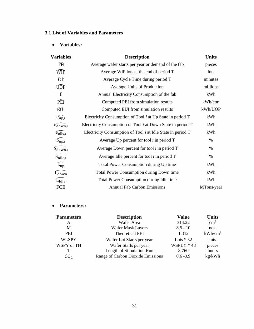
3.1 List of Variables and Parameters
Variables:
Variables Description Units
TH Average wafer starts per year or demand of the fab pieces
WIP Average WIP lots at the end of period T lots
CT Average Cycle Time during period T minutes
UOP Average Units of Production millions
L Annual Electricity Consumption of the fab kWh
PEI Computed PEI from simulation results kWh/cm2
EUI Computed EUI from simulation results kWh/UOP
eup,i Electricity Consumption of Tool i at Up State in period T kWh
edown,i Electricity Consumption of Tool i at Down State in period T kWh
eidle,i Electricity Consumption of Tool i at Idle State in period T kWh
Sup,i Average Up percent for tool i in period T %
Sdown,i Average Down percent for tool i in period T %
Sidle,i Average Idle percent for tool i in period T %
Lup Total Power Consumption during Up time kWh
Ldown Total Power Consumption during Down time kWh
LIdle Total Power Consumption during Idle time kWh
FCE Annual Fab Carbon Emissions MTons/year
Parameters:
Parameters Description Value Units A Wafer Area 314.22 cm2
M Wafer Mask Layers 8.5 - 10 nos.
PEI Theoretical PEI 1.312 kWh/cm2
WLSPY Wafer Lot Starts per year Lots * 52 lots
WSPY or TH Wafer Starts per year WSPLY * 48 pieces
T Length of Simulation Run 8,760 hours
CO2 Range of Carbon Dioxide Emissions 0.6 -0.9 kg/kWh

32
3.2 Capacity Performance Measures
Cycle Time (CT):
Cycle time can be defined as the average time from release of the job at the
beginning of the routing until it reaches an inventory point at the end of the routing or time
that part spends as a work in progress [31]. It can also be defined as the time taken to
complete the production of one unit from the beginning to end.
Throughput (TH):
For a production line, throughput is defined as the average quantity of good parts
produced per unit time [31].
Work-in-Process (WIP):
Work-in-Process is defined as the inventory between the start and end points of a
product routing. It can be used as one parameter to calculate and measure efficiency [31].
Little’s Law:
Little’s law describes the essential relationships among WIP, CT, and TH. The
power of Little’s law lies in its ability to influence team behavior with its underlying
constraints [31]. It helps the user to use a given scale to benchmark actual production
systems. For instance, to increase the throughput of a production line limit the WIP in the
system or speed up the process to once again limit the WIP. The fundamental relationship
between WIP, CT, and TH over the long-term is:
WIP = TH × CT (1)

33
Units of Production (in millions):
The units of production (UOP) of a fab are defined as:
UOP = TH × A × M (2)
The number of mask layers is used to represent the complexity of production.
Number of masks is directly proportional to the number of processes required to produce
a wafer. Considering the throughput or wafer starts (TH), wafer surface area (A), and an
average number of mask layers (M), Units of Production (UOP) gives a good estimate of
the total production capability of a wafer fab [45].
3.3 Electricity Consumption Metrics
The characterization of power consumption of a wafer fab is defined by the
following performance metrics.
1. Production Efficiency Index (PEI)
2. Electrical Utilization Index (EUI)
The performance metrics can also be used to track the efficiency trends associated
with products that are evolving. These efficiency indicators are largely defined using
normalization methods, i.e., dividing electric power consumption of the wafer plants or
tools by a unit measuring the scales of wafer production (e.g., number of units or wafer
area).
34
Production Efficiency Index:
Production Efficiency Index (PEI with a unit of kWh/cm2) is defined as a fab’s total
annual electricity consumption divided by its total wafer surface area produced. It
represents the energy efficiency of a fab without including the complexity of the wafer
production, but the physical scales of wafer area are processed.
PEI = L
TH × A
(3)
Electrical Utilization Index:
Electrical Utilization Index (EUI with a unit of kWh/UOP) is defined as a fab’s total
annual electric power consumption divided by its annual UOP. EUI quantifies the energy
efficiency of how a fab uses electric power consumption for wafer production, which
considers the wafer process complexity.
EUI = L
UOP (4)
3.4 Comparison of PEI and EUI
PEI and EUI are defined to quantify and compare the energy efficiency of the fabs.
The efficiency trends associated with products evolving over time can be tracked by using
the above-mentioned performance metrics. These performance indicators are normalized
based on dividing electric power consumption of the wafer plants or tools by the number
of units or wafer area. Notably, PEI is similar to EUI except that the number of mask layers
is not considered. The mask layers define the complexity of the processes. The number of
mask layers is proportional to the number of processes required to produce a wafer.
Therefore, PEI index does not represent the complexity of the product, only the quantity of
wafer area [45].

35
3.5 Capacity Model for Electrical Power Consumption Estimation using WIP Lot
Data (kWh-WIP)
The model presented by formulas in Equations (1) -(7) calculates power
consumption by using WIP-lot data, UOP and PEI values.
kWh-WIP Model:
UOP = WIP
CT× A × M
(5)
L (kWh) = PEI × TH × A (6)
L (MW) = L(kWh)
T
(7)
where T is the number of hours in the simulation run.
In Equation (5), WIP represents the average number of lots that are being processed
during a simulation run. This is a critical input for energy consumption calculations. Using
Little’s Law in Equation (1), average cycle time gives average throughput. Therefore, the
units of production for this particular fab model is computed based on the wafer area and
the number of mask layers in this process. With electric energy consumption guidelines for
WIP and the selected optimal PEI value, the computed throughput TH, and wafer area
energy consumption of the fab is calculated. The total annual power consumption of the
fab L (kWh) is computed from equation (6). Equation (7) represents the load of the fab in
MW. This value is obtained from computed load L (kWh) divided by the simulation period

36
in hours. Furthermore, other performance parameters like EUI is computed with the
theoretical PEI and wafer mask layers (M).
3.6 Capacity Model for Electrical Power Consumption Estimation using Tool-level
Utilization (kWh-Tool)
This method in Equations (8) -(13) estimates the energy consumption of a wafer
fab by analyzing the energy utilization of each station-process.
kWh-Tool Model:
Lup = ∑ ∑ eup,i × Sup,i
72
𝑖𝑇
(8)
Lidle = ∑ ∑ eidle,i × Sidle,i
72
𝑖𝑇
(9)
Ldown = ∑ ∑ edown,i × Sdown,i
72
𝑖𝑇
(10)
L = L𝑢�� + L𝑑𝑜𝑤�� + L𝑖𝑑𝑙�� (11)
Where L is the annual power consumption of the fab
PEI =L
TH × M
(12)
Where TH is the throughput or the wafer starts per year of the fab.
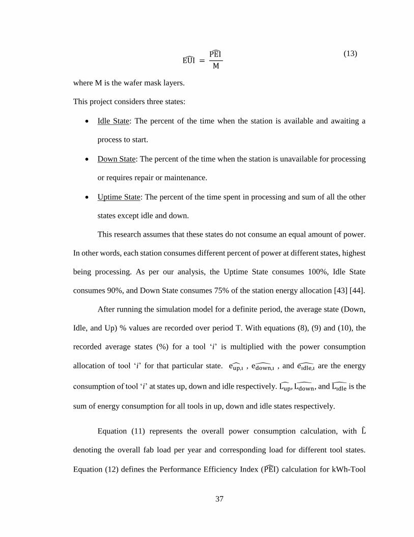
37
EUI = PEI
M
(13)
where M is the wafer mask layers.
This project considers three states:
Idle State: The percent of the time when the station is available and awaiting a
process to start.
Down State: The percent of the time when the station is unavailable for processing
or requires repair or maintenance.
Uptime State: The percent of the time spent in processing and sum of all the other
states except idle and down.
This research assumes that these states do not consume an equal amount of power.
In other words, each station consumes different percent of power at different states, highest
being processing. As per our analysis, the Uptime State consumes 100%, Idle State
consumes 90%, and Down State consumes 75% of the station energy allocation [43] [44].
After running the simulation model for a definite period, the average state (Down,
Idle, and Up) % values are recorded over period T. With equations (8), (9) and (10), the
recorded average states (%) for a tool ‘i’ is multiplied with the power consumption
allocation of tool ‘i’ for that particular state. eup,i , edown,i , and eidle,i are the energy
consumption of tool ‘i’ at states up, down and idle respectively. Lup, Ldown, and Lidle is the
sum of energy consumption for all tools in up, down and idle states respectively.
Equation (11) represents the overall power consumption calculation, with L
denoting the overall fab load per year and corresponding load for different tool states.
Equation (12) defines the Performance Efficiency Index (PEI) calculation for kWh-Tool

38
methodology. In this equation, ‘TH’ is the capacity or defined as wafer starts per year of
the fab, and ‘M’ is wafer masks layers. With the annual power consumption of the fab and
the wafer area with demand, the PEI metric is computed. Further, Electrical Utilization
Index EUI is defined in equation (13), with (PEI) divided by the number of mask layers.
The goal is to show the relationship between theoretical PEI and computed PEI; to validate
the kWh-Tool methodology.
3.7 Carbon Dioxide Emission Calculation
In order to supply the calculated amount of electricity, the amount of carbon dioxide
released by fossil fuel-fired power plants, etc. is estimated to be 180–360 metric tons per
day. This estimation is made based on the factor that 0.6–0.9 Kg is released when 1 kWh
electricity is produced from a fossil fuel-fired power plant [2]. Assuming the carbon
emission to be 0.6-0.9 kg for 1 kWh of electric energy, equation (14) calculates the annual
carbon emission is calculated for every fab type expressed in terms of metric tons per year.
FCE (𝑚𝑒𝑡𝑟𝑖𝑐 𝑡𝑜𝑛𝑠
𝑦𝑒𝑎𝑟) = CO2 × L
(14)
Where, FCE is the amount of carbon emissions recorded by the fab in a year (in
metric tons per year) and
CO2 emission range vs. power consumption is set between = 0.6 − 0.9 Kg/kWh
3.8 Description of Simulation Model
The MIMAC was a joint project of JESSI/MST and SEMATECH to identify and
measure the effects and interactions of major factors that cause a loss in fab efficiency
(Fowler and Robinson, 1995) [46]. This research uses the MIMAC reference model to

39
analyze the electricity utilization in a 200mm semiconductor wafer fab. Inputs and outputs
for the model are shown in Figure 5.
Figure 5 Inputs and Outputs for the MIMAC Model
Nine different fab scenarios are identified based on wafer starts per year and
product mixes with the MIMAC dataset. The demand for the fab is represented by wafer
starts per year. The product mixes correspond to the ratio of production between Part A vs.
Part B. The technology usage and MIMAC simulation model set up is discussed in section
3.10.
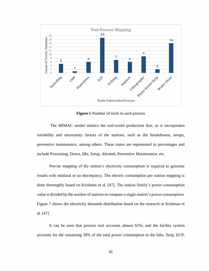
The MIMAC dataset comprises 71 station families and 220 stations. These station
families include Lithography, Annealing, ECP, CMP, Etching, Deposition, Photo-resist
strip, wafer clean and implant. Table 1 summarizes the station family to process mapping.
Figure 6 depicts the number of stations per station family.
Inputs
Tools
Routing
Part
Options
Order
Setup
MIMAC
AutoSched
Outputs
Cycle Time
WIP lots
Processing %
Down %
Idle %
Station Use

40
Table 1 Station Family –Process Mapping
1. Implant 2. Deposition 3. Etching
GENUS
HIGH_CURREN
T_IMP
IMPLANT_OX
MED_CURRENT
_IMP
POLY_DOPE
VARIAN
BPSG
DELAMINATOR
LAMINATOR
LTO
OXIDE_1
SILICIDE_TOOL
AME_8310
AME_8330
E_SINK
MATRIX
OXIDE_LAM
POLY_LAM
RAINBOW_4500
4. ECP 5. Wafer Clean 6. Lithography
ANELVA
BARRIER_OX
CD_MACH
DRIVE_OX
FIELD_OX
FINAL_VISUAL
GATE
INTERGATE
LASER_SCRIBE
LEITZ_ETCH
LEITZ_LITHO
NANOSPEC
NITRIDE
PEAK
POLY_DEP
PROMETRIX
QUAESTAR
DIFF_SINK1
DIFF_SINK2
DIFF_SINK3
DIFF_SINK4
DIFF_SINK5
DIFF_SINK6
DIFF_SINK7
DIFF_SINK8
FSI
METAL_SINK
SINK_22_BOE
SINK_22_CAROS
SINK_24_BOE
SINK_24_CAROS
ULTRASONIC_C
LEAN
ULTRASONIC_T
OOL
ALIGNER
CRIT_COAT
CRIT_DEV
NONCRIT_COAT
NONCRIT_DEV
SECOND_MASK
STEPPER
VAPOR_PRIME_O
VEN
NEW_STEPPER
7. Annealing 8. Photo-Resist Strip 9. CMP
ALLOY
REFLOW
UV_BAKE
UV_BAKE_BAC
KEND
VWR_OVEN
BRANSON
STRIPPER
BACKGRIND
41
Figure 6 Number of tools in each process
The MIMAC model mimics the real-world production line, so it incorporates
variability and uncertainty factors of the stations, such as the breakdowns, setups,
preventive maintenance, among others. These states are represented in percentages and
include Processing, Down, Idle, Setup, Aborted, Preventive Maintenance, etc.
Precise mapping of the station’s electricity consumption is required to generate
results with minimal or no discrepancy. The electric consumption per station mapping is
done thoroughly based on Krishnan et al. [47]. The station family’s power consumption
value is divided by the number of stations to compute a single station’s power consumption.
Figure 7 shows the electricity demands distribution based on the research in Krishnan et
al. [47].
It can be seen that process tool accounts almost 61%, and the facility system
accounts for the remaining 39% of the total power consumption in the fabs. Strip, ECP,
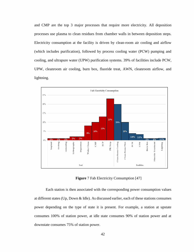
42
and CMP are the top 3 major processes that require more electricity. All deposition
processes use plasma to clean residues from chamber walls in between deposition steps.
Electricity consumption at the facility is driven by clean-room air cooling and airflow
(which includes purification), followed by process cooling water (PCW) pumping and
cooling, and ultrapure water (UPW) purification systems. 39% of facilities include PCW,
UPW, cleanroom air cooling, burn box, fluoride treat, AWN, cleanroom airflow, and
lightning.
Figure 7 Fab Electricity Consumption [47]
Each station is then associated with the corresponding power consumption values
at different states (Up, Down & Idle). As discussed earlier, each of these stations consumes
power depending on the type of state it is present. For example, a station at upstate
consumes 100% of station power, at idle state consumes 90% of station power and at
downstate consumes 75% of station power.

43
3.9 Selection of Optimal PEI value
Hu et al. [12] characterized the energy consumption for several wafer fabs with
different UOPs. The MIMAC simulation analyzed in this paper is similar to the fab
performance metrics considered for a 200mm wafer fab and 9 different fab profiles. This
paper thus assumes that the PEI for the MIMAC model is 1.213 kWh/cm2, as in the
150/200mm wafer fab study in Taiwan 1999.
Table 2 Wafer Fab Production and Energy Indices [9]
300mm 150/200 mm 150/200mm 200mm 300mm
Fab location/year Taiwan
2007 Taiwan 1999
Worldwide
1999
Worldwid
e 2007
Worldwide
2007
Total number of
fabs 4 9 14 5 5
Annual UOP
value (in millions) 14,552 313 299 4178 5666
EUI (kWh/UOP) 0.027 0.058 0.0609 0.0477 0.0461
PEI (kWh/cm2) 0.743 1.213 1.15 1.295 2.133
3.10 Simulation Process
As discussed in section 3.5, the MIMAC dataset is built on AutoSched discrete
event simulation platform. AutoSched is a finite capacity planning and scheduling tool that
helps to increase throughput, reduce the in-process inventory and increase equipment and
personnel utilization. It uses AutoMOD system simulation as a foundation because this
provides 3D graphics, discrete event simulation environment, and material handling.

44
In a model, information about the factory operations is divided into three general
categories; resources, products, and demand. Resources consist of the items used to
manufacture the desired parts. The primary resources considered in the model include
stations and operators. As explained in the previous sections, the model incorporates 71
station family and 220 stations/tools in the production lines. The processing times at the
work centers/stations are deterministic and depend on the number of wafer in a lot. Goods
manufactured by the factory are called as products, and lots consisting of 48 wafers are the
moving entities in the designed wafer fab. Even though traditional wafer fabrication
facilities use 25 wafers per lot, the MIMAC data set is designed with 48 wafers in a lot.
This increase in lot size would accommodate the growing demand and satisfy the need to
increase the capacity of fab. Essential information about the products is incorporated into
the model such as parts, route, and bill of materials. The parts file describes the type of
product manufactured. The routing methodology includes the station routing logic that
particular part type follows. And the bill of materials describes the consumption of sub-
parts.
Some of the semiconductor manufacturing characteristics such as unreliable,
parallel stations, reentrant flows, sequence set-up times, batch processing are considered.
In this model, batch processing is termed as a group of lots that are processed at the same
time on a single machine. The batch processing stations have a minimum and maximum
batch sizes where only lots of the same product and at the same operation can be batched
together. Two products (Part A and Part B) are modeled with 200 operations completion.
The model contains over 200 stations in a production line, which are structured in and
around 70 work centers. A rapid material transfer between the stations with successive

45
operations is assumed. Also, the stations follow a First-In-First-Out (FIFO) dispatching
rule. The Mean Time Between Failures (MTBF) of the stations are considered as an
individual or unrelated event, therefore breakdowns are modeled with an exponential
distribution.
Demand information is incorporated in the model in terms of orders and describes
a group of lots. The demand information or wafer starts per year of the fab is represented
as repeats value and product mixes. The repeats value in minutes is obtained based on
product mix and demand plan. This value is fed as an input to the model. The simulation
length and replications are defined based on the snap length and number of snaps in the
model.
The performance reports include the parameters recorded from the simulation
model execution. The parameters include station utilization (Idle%, Downtime%,
Processing%, etc.), average lots per week, average cycle times. The results from the
simulation model are used with the equations described in earlier sections to compute the
annual power consumption and other performance metrics using kWh-WIP and kWh-Tool
methodologies. Figure 8 illustrates the overview of the computational process.
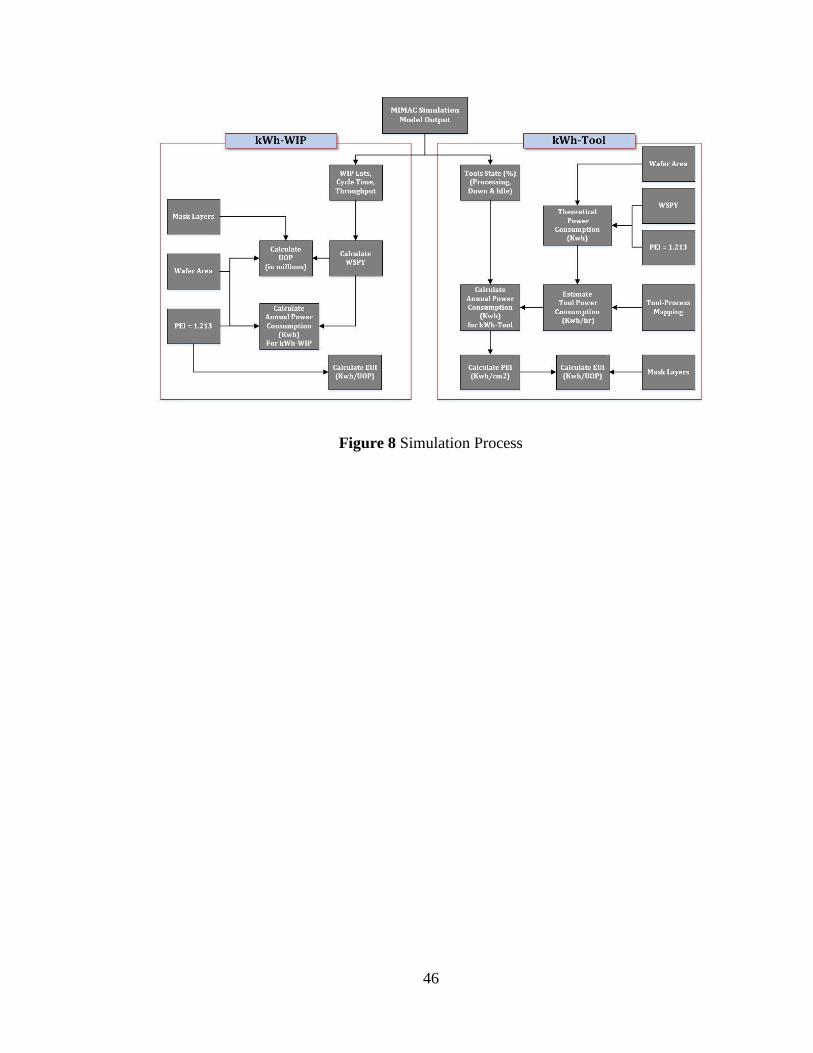
46
Figure 8 Simulation Process

47
4. RESULTS AND DISCUSSIONS
In this chapter, simulation results and computed performance metrics for both
methodologies are discussed and compared by performing Design of Experiments. The
results from the simulation are used to compute the annual power consumption and carbon
dioxide emissions. Different fab profiles are generated based on factors, such as wafer
starts per year and product mix, and the proposed methodologies are applied to each of
them.
4.1 Design of Experiments
The design of experiments considered two factors, namely Wafer Starts per Year
and Product Mix.
Wafer lots starts per year: This factor describes the fab’s capacity and the annual
demand and its units are expressed in pieces.
Product Mix: This factor represents the ratio of Part A vs. Part B manufactured for a
particular demand. The simulation model is built based on a manufacturing line that
handles two types of parts or wafers. Each type of wafer has a particular set of processes
and routing defined in the model. Varying this factor changes the number of processing
steps that will be required to complete the required product demand, thus increasing
the total cycle time.

48
Total of nine scenarios or fabs were identified based on wafer lots starts per year
and product mixes. Table 3 shows the scenarios concerning the different factor
combinations considered.
Table 3 Fab Profile Definition
Fab Scenario WLSPY (Lots)
Product Mix
Part A Part B
A1 2610 50% 50%
A2 2610 100% 0%
A3 2610 25% 75%
B1 2755 50% 50%
B2 2755 100% 0%
B3 2755 25% 75%
C1 2900 50% 50%
C2 2900 100% 0%
C3 2900 25% 75%
The notations A, B, and C represent three types of wafer lot starts per year namely
2610, 2755 and 2910 respectively. Further, the notations 1, 2, and 3 represent product
mixes 50-50%, 100%-0%, and 25%-75% product mixes respectively.

49
4.2 Design of Simulation Experiment
Scenarios are differentiated in the simulation model by a repeats factor represented
in minutes. The repeats are calculated based on wafer lots per year (demand), and the
product mixes are fed as input to the simulation model. The repeats represent the inter-
arrival times between the parts that are introduced into the system. As mentioned, these
repeats or inter-arrival are calculated based on the demand plan scenario. Table 4 below
represents the repeats value for part A and Part B based on a wafer lot starts per year and
product mix.
Table 4 Repeats Calculation for Each Scenario or Fab Type
WLPY WLSPY Product Mix:
50%-50%
Product Mix:
100%-0%
Product Mix:
25%-75%
RPT_A
(mins)
RPT_B
(mins)
RPT_A
(mins)
RPT_B
(mins)
RPT_A
(mins)
RPT_B
(mins)
2755 132240 381.56 381.56 190.78 5,080,320 763.12 254.37
2610 125280 402.76 402.76 201.38 5,080,320 805.52 268.51
2900 139200 362.48 362.48 181.24 5,080,320 724.97 241.66
The length of each simulation replication is one week, and the model is replicated
250 times. The replications are independent to each another. A higher repeats value is
considered for a scenario with a product mix of 0%. In other words, a value close to twice
the length of the simulation run is considered to ensure that the product is never released.
For instance, the total length of the simulation is 250 weeks, and it corresponds to
2,520,000 minutes. The repeats value for a product mix of 0% would be twice of this, as
seen in the above table.

50
4.3 Results for the kWh-WIP
As discussed in the earlier chapter, the Capacity Model for Power Consumption
Estimation using WIP-Lot Data (kWh-WIP) method is used to represent energy
consumption of a wafer fab by analyzing the energy utilization of each process in a
semiconductor wafer fab. The WIP lot results obtained from the simulation model are
analyzed based on the performance indices. The length of simulation is one week, and each
scenario or fab type is run for 248 weeks or snaps. Figure 9 captures WIP lots recorded for
each simulation replication for all the fab types.
Figure 9 WIP lots recorded across scenario runs for every fab type

51
The above figure shows the WIP lots recorded between each replication for all fabs
considered. The lines with non-increasing trend represent stable simulations, thus, for the
considered WLSPY and product mix, the scenario is feasible. One of the Fab C3 records a
higher or increasing line, which denotes that the simulation runs are unstable, and the
bottleneck utilization recorded is over 100%.
With the equations established and explained in Chapter 3, as part of this proposed
methodology power consumption and other performance metrics are calculated. In the
below pages, Tables 5 describes the power calculation for the methodology and Tables 6
and 7 defines the EUI and PEI calculation for this methodology. A cycle time factor is
established to convert WIP lots per week to WIP lots starts per year. The cycle time
recorded in minutes as an average of all 248 replications is defined as the time taken to
produce the desired lots per week.

Table 5 Power Consumption Calculation for the kWh-WIP method
Fab A1 Fab A2 Fab A3 Fab B1 Fab B2 Fab B3 Fab C1 Fab C2 Fab C3
Weeks 248 248 248 248 248 248 248 248 248
IS
SIMULATION
RUN STABLE
(Y/N)?
Y Y Y Y Y Y Y Y N
WIP Lots per
Week 162.0 133.4 185.4 174.5 141.1 329.9 196.0 150.8 892.7
Avg. CT (mins) 3.2 2.7 3.7 3.3 2.7 6.3 3.39 2.62 15.5
CT in weeks 50.3 49.4 50.1 53.0 52.4 52.8 57.8 57.6 57.7
Throughput 2615.3 2568.9 2605.9 2758.1 2727.1 2744.8 3007.2 2993.4 3002.5
Wafers per Lot
(pieces) 48.0 48.0 48.0 48.0 48.0 48.0 48.0 48.0 48.0
Mask Layers 8.5 7.0 9.3 8.5 7.0 9.3 8.5 7.0 9.3
Wafer Area (cm2) 314.2 314.2 314.2 314.2 314.2 314.2 314.2 314.2 314.2
WSPY 125536.5 123306.6 125083.6 132390.3 130899.1 131750.3 144343.4 143685.5 144122.3
UOP (in Millions) 335.2M 271.1M 363.4M 353.5M 287.8M 382.8M 385.4M 316M 418.8M
52

Table 6 PEI Analysis for the kWh-WIP method
Fab
A1
Fab
A2
Fab
A3
Fab
B1
Fab
B2
Fab
B3
Fab
C1
Fab
C2
Fab
C3
Theoretical
PEI 1.213 1.213 1.213 1.213 1.213 1.213 1.213 1.213 1.213
Total
Consumption
(MWh)
47,838 46,989 47,666 50,450 49,882 50,206 55,005 54,755 54,921
Load (MW) 5.5 5.4 5.4 5.8 5.7 5.7 6.3 6.3 6.3
Table 7 EUI Analysis for the kWh-WIP method
Fab
A1
Fab
A2 Fab A3
Fab
B1
Fab
B2
Fab
B3
Fab
C1
Fab
C2
Fab
C3
EUI 0.143 0.173 0.131 0.143 0.173 0.131 0.143 0.173 0.131
Total Power
Consumption
(MWh)
47,838 46,989 47,666 50,450 49,882 50,206 55,005 54,755 54,921
Load (MW) 5.5 5.4 5.4 5.8 5.7 5.7 6.3 6.3 6.3
53

54
4.4 Results for the kWh-Tool
This methodology analyzes the tool-process utilization and aims to compute the annual
power consumption and performance metrics of the fabs. Tool-level energy consumption is
estimated based on tool-process mapping and the optimal PEI value selection. Like the kWh-WIP
method, this method also aims to calculate annual power consumption and performance metrics
for the identified nine fab types.
The study assumes three states namely, Up State, Down state and Idle State in the
percentage of the time. Apart from the above-mentioned equipment states, the simulation model
also records states such as starving, blocked, and collecting. To simplify the constraints, this study
assumes these states to be a part of uptime states. Overall, the three states add up to a total of 100%.
Efficiency factors of the tools/stations are difficult to obtain or estimate. Upon intensive research,
the efficiency factors are assumed for each state of the tools. For example, Uptime consumes
100%, idle state consumes 90% and down state consumes 75% of the total tool power consumption
value respectively.
The tables summarizing the detailed simulation results by tool level are shown in Appendix
A, Tables A1-A9. The model displays the station-process state utilization percentage recorded over
a period of one week (as one replication length is one week, and the model is run for 248 weeks).
The values are represented in percentage and is the average of 248 replications or weeks.

55
4.5 Comparison between kWh-WIP vs. kWh-Tool
With the equations established and explained in Chapter 3 as a part of this proposed
methodology, power consumption and other performance metrics are calculated. Table 8 compares
the fab profiles with computed annual power consumption and performance metrics values using
the kWh-WIP and the kWh-Tool simulation methods. Table 9 summarizes the annual power
consumption values of these two methods, and figure 10 depicts the same results. The findings are
summarized below:
The annual power consumption values calculated from kWh-WIP is slightly higher
compared to kWh-Tool.
Power consumption calculation in both methodologies increases with wafer starts per year.
This is a factor for the validation of the simulation model and methodology.
In both the methodologies, the product mixes 50%-50% and 25%-75% have higher power
consumption values compared to the product mix 100%-0%. This gives us an estimate that
stations or processes involved with part B manufacturing consume higher power.
kWh-WIP gives higher estimates of power consumption for the 50%-50% product mixes
when compared to the other fab type with similar wafer starts per year i.e. the energy
consumption decreases when the product mix is changed from 50%-50% for a particular
WSPY fab type. However, the same behavior is not observed consistently with kWh-Tool
as the value tends to slightly increase for 25%-75% product mix. An exception to this is
Fabs C1, C2 and C3 with the product mix 50%-50%, where a higher value is observed
compared to others. This inconsistency is due to the energy efficiency and power
consumption estimate of tools.

Table 8 Fab Profile Comparison
Fab
Wafer
Diameter
(mm)
Wafer
Lots
Starts
Per
Year
Wafer
Starts
per
year
Wafe
r
mask
layer
s
Wafer
Area
(cm2)
kWh-WIP kWh-Tool
Wafer
Starts
per year
UOP
Annual
Power
Consumption
(kWh)
PEI EUI
Annual
Power
Consumption
(kWh)
PEI EUI
A1 200 2610 125280 8.5 314.16 125536 335,226,757 47,838,942 1.21 0.14 46,522,160 1.18 0.13
A2 200 2610 125280 7.0 314.16 123307 271,165,485 46,989,215 1.21 0.17 46,466,684 1.18 0.16
A3 200 2610 125280 9.3 314.16 125084 363,489,595 47,666,369 1.21 0.13 46,539,040 1.18 0.12
B1 200 2755 132240 8.5 314.16 132390 353,528,845 50,450,764 1.21 0.14 49,156,794 1.18 0.13
B2 200 2755 132240 7.0 314.16 130899 287,862,066 49,882,500 1.21 0.17 49,091,887 1.18 0.16
B3 200 2755 132240 9.3 314.16 131750 382,862,880 50,206,893 1.21 0.13 49,166,772 1.18 0.12
C1 200 2900 139200 8.5 314.16 144343 385,447,835 55,005,802 1.21 0.14 53,913,742 1.23 0.13
C2 200 2900 139200 7.0 314.16 143685 315,980,892 54,755,103 1.21 0.17 53,838,833 1.23 0.16
C3 200 2900 139200 9.3 314.16 144122 418,815,661 54,921,577 1.21 0.13 53,863,411 1.23 0.12
56

57
Table 9 Annual Power Consumption values for kWh-WIP and kWh-Tool
Fab PC (kWh) - kWh-WIP PC (kWh) - kWh-Tool
Fab A1 46,522,160 47,838,942
Fab A2 46,466,684 46,989,215
Fab A3 46,539,040 47,666,369
Fab B1 49,156,794 50,450,764
Fab B2 49,091,887 49,882,500
Fab B3 49,166,772 50,206,893
Fab C1 53,913,742 55,005,802
Fab C2 53,838,833 54,755,103
Fab C3 53,863,411 54,921,577
Figure 10 Annual Power Consumption for kWh-WIP and kWh-Tool
42,000,000
44,000,000
46,000,000
48,000,000
50,000,000
52,000,000
54,000,000
56,000,000
Fab A1 Fab A2 Fab A3 Fab B1 Fab B2 Fab B3 Fab C1 Fab C2 Fab C3
Po
wer
Co
nsu
mp
tio
n (
kW
h)
Annual Power Consumption - kWh-WIP vs. kWh-Tool
kWh-WIP kWh-Tool

58
4.6 Error %
Table 10 summarizes the difference in annual power consumption values between
both the methodologies expressed in terms of error percentage.
Table 10 Annual Power Consumption Error % between kWh-WIP and kWh-Tool
As observed, the error estimate is less than 3% across all fab types. Below are the
reasons identified:
Tool Level Power Consumption Estimate: This study included a tool process
mapping based on intensive research and surveying. As the tool level estimates are
difficult to obtain, the study assumed values based on strong research. Yet, there could
be discrepancies between the simulation model tool set up and the literature available.
Efficiency Factors of the Station: Efficiency of each tool in the model can also be an
important factor contributing to the variation in power consumption values. The
efficiency factors include the tools energy consumption in different states. Tools
consume electricity differently based on the states. For example, down and idle
consume lower than processing state. Upon intensive research on semiconductor tool
efficiency, this study assumed down state consuming 75% and idle state consuming
90% of the tool electricity allocation. On the other hand, supplemental states such as
Error %
Fab A1 2.75%
Fab A2 1.11%
Fab A3 2.37%
Fab B1 2.56%
Fab B2 1.58%
Fab B3 2.07%
Fab C1 1.99%
Fab C2 1.67%
Fab C3 1.93%

59
blocked, starved, collecting, etc. were assumed to be consuming the same percentage
of electricity as the up state.
4.7 Insights of kWh-WIP
kWh-WIP is based on little’s law principle. The average throughput time through a
production system is directly proportional to average inventory based on Factory
Physics and dynamics [31].
Work in Progress (WIP) = Cycle Time (CT) ∗ Throughput (TH)
This gives us an estimate of the number of wafer starts per year, to compute the
power consumption.
An optimal Production Efficiency Index (PEI) value is required to estimate an
accurate power consumption. On the other hand, a bad PEI value could lead to an
inaccurate estimate of the fab’s power consumption.
4.8 Insights of kWh-Tool
kWh-Tool methodology has a more in-depth level of detail incorporated in
calculating the power consumption.
This methodology not only incorporates the flow of wafers in the system but also
considers tool utilization, which is the finest level of detail in estimating the power
consumption.
But there are quite a few challenges associated with this methodology. As discussed
earlier, this methodology requires tool level energy consumption data which is

60
difficult to obtain. Also, energy efficiency factors have to be associated with the
equipment for different states recorded by the simulation model.
4.9 EUI Comparison
Figure 11 kWh-WIP EUI vs. kWh-Tool EUI comparison
Figure 11 shows that the EUI values for each method. Part of establishing the
relationship between these two methodologies, the study aims to have similar EUI values.
The EUI values associated with kWh-WIP are calculated from the assumed theoretical PEI
and the mask layers for a particular fab type. With the power consumption calculation from
kWh-Tool and by obtaining relevant PEI results in an EUI value closer to the kWh-WIP
EUI. However, the slight variation is due to the computed PEI which is influenced by the
variation in the annual power consumption values. As mentioned earlier, these values
0.143
0.173
0.131
0.143
0.173
0.131
0.143
0.173
0.131
0.139
0.169
0.128
0.139
0.169
0.128
0.139
0.169
0.128
0.100
0.110
0.120
0.130
0.140
0.150
0.160
0.170
0.180
Fab A1 Fab A2 Fab A3 Fab B1 Fab B2 Fab B3 Fab C1 Fab C2 Fab C3
EU
I (k
Wh/U
OP
)
Electrical Utilization Index - kWh-WIP vs. kWh-Tool
kWh-WIP kWh-Tool

61
depend upon mask layers which are represented by the product mixes. Thus, similar product
mixes have similar EUI values in both the methodologies.
4.10 Bottleneck Station Utilization Study
Another goal of this study is to analyze the bottleneck station and the associated
process in each fab type. The AutoSched reports for every scenario of wafer starts per year
and product mix are analyzed to identify the bottleneck station in the processes. The station
with lowest idle percentage is inferred as the bottleneck of the line. The lowest idle
percentage could be due to higher station cycle times or low station availability. Below
table summarizes the details of the bottleneck station.
Table 11 Bottleneck Station-Process and Utilization percentage for each fab type
Fab Utilization (%) Station Family Process
Fab A1 80.04% OXIDE_1 Deposition
Fab A2 77.80% OXIDE_1 Deposition
Fab A3 81.98% OXIDE_1 Deposition
Fab B1 90.15% STEPPER Lithography
Fab B2 86.54% STEPPER Lithography
Fab B3 94.50% STEPPER Lithography
Fab C1 99.35% STEPPER Lithography
Fab C2 94.81% STEPPER Lithography
Fab C3 99.46% STEPPER Lithography

62
Figure 12 Bottleneck Station Utilization for each fab type
The bottleneck station utilization increases with the capacity of the fab or the wafer
starts per year
Fabs A1, A2 and A3 records station family OXIDE_1 corresponding to the
Deposition process, while the remaining fabs record STEPPER associated with
Lithography process as bottlenecks.
Lithography and Deposition are the critical processes in semiconductor wafer
fabrication. With a higher utilization recorded from these stations, they also
correspond to higher consumption of energy and emission of carbon dioxide.
Optimization projects could be directed towards these bottleneck stations and
process to achieve energy efficiency and reduction in carbon emissions.
80.04%77.80%
81.98%
90.15%
86.54%
94.50%
99.35%
94.81%
99.46%
50%
55%
60%
65%
70%
75%
80%
85%
90%
95%
100%
Fab A1 Fab A2 Fab A3 Fab B1 Fab B2 Fab B3 Fab C1 Fab C2 Fab C3
Uti
liza
tio
n (
%)
Bottleneck Station Family Utilization

63
4.11 CO2 Emission Calculation
The final part of this research aims to estimate and study the carbon dioxide
emissions from the semiconductor fabs. As wafer fabrication is an energy-intensive
process, the fabs consume a lot of electricity. In order to supply the calculated amount of
electricity, the amount of carbon dioxide released by fossil fuel-fired power plants, etc. is
estimated to be 180–360 metric tons per day. This estimation is made based on the factor
that 0.6–0.9 Kg is released when 1 kWh electricity is produced from a fossil fuel-fired
power plant [2]. Assuming the carbon emission to be 0.6-0.9 kg for 1kWh of power, the
annual carbon emission is calculated for every fab type expressed in terms of metric tons
per year.
The carbon dioxide emission calculations are computed based on the annual power
value obtained from the kWh-WIP methodology. The reason behind the preference of
kWh-WIP over kWh-Tool is due to the variation explained earlier. Furthermore, kWh-WIP
is a quick and accurate estimate of power consumption with minimal challenges.

64
Table 12 Carbon Dioxide Calculation for Fabs based on kWh-WIP
Fab 0.6 Kg/kWh
CO2 Emissions (MTons/year)
0.9 Kg/kWh
CO2 Emissions (MTons/year)
Fab A1 28,703 43,055
Fab A2 28,194 42,290
Fab A3 28,600 42,900
Fab B1 30,270 45,406
Fab B2 29,930 44,894
Fab B3 30,124 45,186
Fab C1 33,003 49,505
Fab C2 32,853 49,280
Fab C3 32,953 49,429
Figure 13 Carbon Emissions per year visualization for the different fab types

65
As shown in Figure 13 and the results in Table 12, the carbon dioxide emissions
increase with higher fab demand or wafer starts per year. With the computed annual power
consumption, the carbon dioxide emissions would lie in between the lines for a particular
fab type.

66
5. CONCLUSION AND FUTURE WORK
5.1 Conclusion
Semiconductor industries are highly energy-intensive. As wafer fab consumes
about 300-400 MWh/day if electricity is generated by burning fossil fuels. The amount of
carbon dioxide released is approximately 180–360 metric tons per day. This emission
causes climate change, depletion of natural resources, and payment of energy cost. This
project characterized annual power consumption for nine 200 mm Minifabs, including the
energy used by overall fab, tools/stations, and processes through field data collection and
performance analysis.
We have compared energy performance and wafer production facility that makes
wafers in production mixes and wafer starts per year based on additional literature research,
additional data compiling and surveying with the professionals from the semiconductor
manufacturing industry. The average Electrical Utilization Index (EUI) and Production
Efficiency Index (PEI) computed with kWh-Tool methodology across all nine 200 mm
fabs considered in this study is 0.145 kWh/UOP and 1.987 kWh/cm2, respectively. The
average annual power consumption is 44,745,707 kWh. Annual power consumption values
calculated in kWh-WIP and kWh-Tool methodologies are closer with a variation of less
than 3%. The PEI values for different fab type computed from the kWh-Tool methodology
is similar to the optimal theoretical value of 1.231 (kWh/cm2). EUI values computed in
kWh-WIP comply with the ones from kWh-Tool. Carbon dioxide calculations are done for
kWh-WIP and it provides a ballpark estimate of emissions for a 200mm fab with assumed
demand plans and product mix. This study suggests that using EUI in calculating energy

67
efficiency levels of MIMAC production can provide more consistent comparisons than
using PEI alone.
5.2 Managerial Decision Making and Impact
The results discussed earlier calls for a rethinking of how we conceptualize and
benchmark efficiency improvements in rapidly evolving sectors of the semiconductor
industry. A high wafer fab load, i.e. a large number of WIP lots, results in significant energy
and manufacturing costs. The simulation model obtains optimal release schedules to drive
production-related and energy decisions. This analysis would drive optimization projects
on higher energy consumption process and tools that would reduce the overall energy cost
of the fab. Improving tool/station's energy efficiency will consume lower electric power
and eventually result in reduced carbon emissions. As discussed in Chapter 2, a tax is
enforced on the manufacturing facilities when it exceeds the carbon emissions limit set
under regulations. On the other hand, if a fab is sustainable and is able to restrict the carbon
emissions below the limits, carbon credits are awarded. These credits can be traded and
could result in the overall reduction in operating and overhead costs of the fab. It also
provides an opportunity for economic optimization and a sustainable facility design.
Environmental sustainability-based business practices provide a marketing strategy
for businesses to gain a competitive advantage in the market. Sustainable organizations are
effective in engaging with external stakeholders and employees [48]. Further,
semiconductor companies are pushing towards standards such as U.S Green Building
Council’s LEED (Leadership in Energy and Environmental Design) which are aimed at
reducing resource use, designing sustainable facilities and a high-performance work
environment [49].

68
5.3 Future Work
More accurate inputs to the kWh-Tool methodology:
As discussed in the chapter before, the variation in annual power consumption and
the corresponding error percentage are caused due to energy efficiency factors and data
related to tool level energy consumption. With further research and availability of real-time
industry-based data, we can infeed these factors with higher precision to obtain more
accurate power consumption estimates. Further, this would make the capacity model more
robust, and the relationship between each methodology can be established with no errors.
Considering Different Fab Types:
This study considers a 200mm wafer fab production and a set of demand plans or
wafer starts per year and product mixes. Scenarios were created based on this to represent
each fab type. However, the fab scenario consideration can be expanded more, with the
inclusion of 300mm or 450mm fabs and create additional fab profiles based on different
product mixes and wafer starts of the fab. The corresponding studies and comparisons
would be interesting to review and could open up for fab profile optimization.
Estimate Fixed and Variable Load of the fab:
Another interesting way to estimate the power consumption is by calculating the
fixed and variable loads of the fab. Based on PEI, the minimum unit consumption per wafer
is estimated, and the minimum units of production vs. actual production can be compared.
This comparison would show the gap in the production or lost capacity. The gap can be
associated with inefficiencies at the stations, downtimes, queues, etc. By establishing this
relationship, we can access the amount of electricity consumption lost by these

69
inefficiencies. This drives optimization projects and direct cost savings for the
semiconductor industries.
Probability Distribution Methodology for Power Consumption Estimate:
Intensive research lead to the identification of another level of detail or
methodology to estimate the annual power consumption of the fab using probability
distribution. This would be a superficial level of detail compared to the two methodologies
proposed in this thesis. It would be interesting to establish and observe the relationship
among all three methodologies. The below diagram depicts the methodologies and the
anticipated interactions.
Figure 14 Methodologies and Anticipated Interactions in this study

70
APPENDIX SECTION
A. Simulation Results for Tool Utilization for Different Fabs
FAB A1:
Table A1 Simulation Results for Tool Utilization for FAB A1
Tools PROCESS
Utilization (%)
Idle (%) Down
(%)
Up Time
(%)
ALIGNER Lithography 59.65 3.05 37.30
ALLOY Annealing 65.72 3.10 31.18
ALPHASTEP ECP 98.70 0.01 1.29
AME_8310 Etching 57.10 3.58 39.32
AME_8330 Etching 68.12 3.01 28.87
ANELVA ECP 68.93 7.33 23.74
BACKGRIND CMP 87.20 3.00 9.79
BARRIER_OX ECP 34.93 5.81 59.26
BPSG Deposition 48.83 5.11 46.06
BRANSON Photo-Resist
Strip 93.92 0.26 5.82
CD_MACH ECP 87.09 1.01 11.90
CRIT_COAT Lithography 59.84 3.24 36.92
CRIT_DEV Lithography 47.66 3.51 48.83
DELAMINATOR Deposition 56.46 9.99 33.56
DIFF_SINK1 Wafer Clean 83.50 1.74 14.76
DIFF_SINK2 Wafer Clean 51.42 4.94 43.64
DIFF_SINK3 Wafer Clean 91.76 0.88 7.36
DIFF_SINK4 Wafer Clean 75.17 2.79 22.05
DIFF_SINK5 Wafer Clean 75.74 2.32 21.93
DIFF_SINK6 Wafer Clean 85.49 1.64 12.87
DIFF_SINK7 Wafer Clean 95.24 0.37 4.39
DIFF_SINK8 Wafer Clean 79.98 2.53 17.48
DRIVE_OX ECP 43.27 6.02 50.71
E_SINK Etching 46.92 0.64 52.43
FIELD_OX ECP 86.28 1.08 12.64
FINAL_VISUAL ECP 68.69 2.73 28.59
FSI Wafer Clean 49.69 8.91 41.41
GATE ECP 65.18 2.65 32.17
GENUS Implant 60.84 12.86 26.30
HIGH_CURRENT_IMP Implant 37.11 13.21 49.68
IMPLANT_OX Implant 34.85 5.89 59.26
INTERGATE ECP 22.92 7.02 70.05
LAMINATOR Deposition 80.50 4.78 14.73
LASER_SCRIBE ECP 84.45 1.36 14.20

71
Tools PROCESS
Utilization (%)
Idle (%) Down
(%)
Up Time
(%)
LEITZ_ETCH ECP 43.36 2.84 53.80
LEITZ_LITHO ECP 42.22 3.28 54.50
LTO Deposition 28.98 6.90 64.12
MATRIX Etching 51.35 2.61 46.04
MED_CURRENT_IMP Implant 29.60 14.85 55.55
METAL_SINK Wafer Clean 96.58 0.02 3.40
NANOSPEC ECP 89.89 1.42 8.69
NITRIDE ECP 99.98 0.00 0.02
NONCRIT_COAT Lithography 43.69 4.67 51.64
NONCRIT_DEV Lithography 63.39 3.74 32.87
OXIDE_1 Deposition 54.70 2.54 42.77
OXIDE_LAM Etching 71.03 3.12 25.85
PEAK ECP 85.46 1.05 13.50
POLY_DEP ECP 65.97 4.20 29.83
POLY_DOPE Implant 28.68 6.70 64.62
POLY_LAM Etching 45.52 4.31 50.17
PROMETRIX ECP 69.07 2.36 28.57
QUAESTAR ECP 80.41 4.91 14.69
RAINBOW_4500 Etching 66.40 2.44 31.15
REFLOW Annealing 56.60 3.53 39.87
SECOND_MASK Lithography 47.47 3.81 48.72
SILICIDE_TOOL Deposition 60.34 3.35 36.31
SINK_22_BOE Wafer Clean 99.49 0.01 0.50
SINK_22_CAROS Wafer Clean 65.89 0.40 33.71
SINK_24_BOE Wafer Clean 63.48 0.49 36.04
SINK_24_CAROS Wafer Clean 74.14 0.52 25.34
STEPPER Lithography 67.30 0.46 32.23
STRIPPER Photo-Resist
Strip 5.19 13.98 80.83
ULTRASONIC_CLEAN Wafer Clean 100.00 0.00 0.00
ULTRASONIC_TOOL Wafer Clean 94.03 0.63 5.35
UV_BAKE Annealing 98.05 0.01 1.94
UV_BAKE_BACKEND Annealing 66.05 2.29 31.66
VAPOR_PRIME_OVEN Lithography 72.98 1.68 25.34
VARIAN Implant 54.29 3.03 42.68
VWR_OVEN Annealing 66.55 9.74 23.70
WET_PROBE ECP 68.74 0.69 30.57
NEW_STEPPER Lithography 62.57 3.26 34.16

72
FAB A2:
Table A2 Simulation Results for Tool Utilization for FAB A2
Tools PROCESS
Utilization (%)
Idle
(%)
Down
(%)
Up Time
(%)
ALIGNER Lithography 57.77 3.21 39.02
ALLOY Annealing 63.97 3.35 32.68
ALPHASTEP ECP 97.39 0.01 2.59
AME_8310 Etching 56.73 3.62 39.65
AME_8330 Etching 67.80 3.07 29.13
ANELVA ECP 68.58 7.46 23.96
BACKGRIND CMP 87.06 3.07 9.87
BARRIER_OX ECP 43.25 4.95 51.80
BPSG Deposition 49.13 5.07 45.80
BRANSON Photo-Resist
Strip 87.71 0.53 11.76
CD_MACH ECP 86.45 1.01 12.55
CRIT_COAT Lithography 63.02 2.95 34.03
CRIT_DEV Lithography 51.98 3.21 44.81
DELAMINATOR Deposition 55.93 10.24 33.83
DIFF_SINK1 Wafer Clean 83.43 1.74 14.82
DIFF_SINK2 Wafer Clean 52.97 4.83 42.20
DIFF_SINK3 Wafer Clean 91.73 0.88 7.39
DIFF_SINK4 Wafer Clean 75.08 2.79 22.14
DIFF_SINK5 Wafer Clean 75.59 2.32 22.09
DIFF_SINK6 Wafer Clean 87.60 1.32 11.08
DIFF_SINK7 Wafer Clean 96.77 0.29 2.95
DIFF_SINK8 Wafer Clean 79.83 2.53 17.64
DRIVE_OX ECP 61.09 4.15 34.76
E_SINK Etching 53.97 0.61 45.42
FIELD_OX ECP 72.44 2.31 25.25
FINAL_VISUAL ECP 68.36 2.81 28.82
FSI Wafer Clean 66.42 6.67 26.91
GATE ECP 62.21 3.00 34.80
GENUS Implant 74.43 8.76 16.81
HIGH_CURRENT_IMP Implant 40.51 12.60 46.90
IMPLANT_OX Implant 33.62 6.10 60.28
INTERGATE ECP 33.05 6.20 60.75
LAMINATOR Deposition 80.35 4.80 14.85
LASER_SCRIBE ECP 84.38 1.37 14.25
LEITZ_ETCH ECP 49.40 2.50 48.10
LEITZ_LITHO ECP 43.74 3.20 53.06

73
Tools PROCESS
Utilization (%)
Idle
(%)
Down
(%)
Up Time
(%)
LTO Deposition 31.74 6.61 61.65
MATRIX Etching 53.91 2.50 43.58
MED_CURRENT_IMP Implant 35.12 13.76 51.12
METAL_SINK Wafer Clean 96.55 0.02 3.43
NANOSPEC ECP 92.43 1.16 6.41
NITRIDE ECP 99.98 0.00 0.02
NONCRIT_COAT Lithography 51.80 4.07 44.13
NONCRIT_DEV Lithography 61.66 3.91 34.43
OXIDE_1 Deposition 52.54 2.66 44.80
OXIDE_LAM Etching 51.46 5.16 43.38
PEAK ECP 87.70 0.87 11.43
POLY_DEP ECP 65.61 4.24 30.14
POLY_DOPE Implant 33.86 6.31 59.84
POLY_LAM Etching 42.56 4.72 52.72
PROMETRIX ECP 70.37 2.25 27.38
QUAESTAR ECP 86.95 3.20 9.85
RAINBOW_4500 Etching 64.30 2.52 33.18
REFLOW Annealing 70.68 2.47 26.85
SECOND_MASK Lithography 44.87 4.03 51.10
SILICIDE_TOOL Deposition 63.79 2.98 33.23
SINK_22_BOE Wafer Clean 99.76 0.01 0.23
SINK_22_CAROS Wafer Clean 64.51 0.41 35.07
SINK_24_BOE Wafer Clean 65.34 0.46 34.19
SINK_24_CAROS Wafer Clean 67.09 0.59 32.32
STEPPER Lithography 66.05 0.47 33.48
STRIPPER Photo-Resist
Strip 14.36 12.65 72.98
ULTRASONIC_CLEAN Wafer Clean 100.00 0.00 0.00
ULTRASONIC_TOOL Wafer Clean 93.98 0.63 5.39
UV_BAKE Annealing 98.04 0.01 1.95
UV_BAKE_BACKEND Annealing 65.81 2.32 31.87
VAPOR_PRIME_OVEN Lithography 72.77 1.68 25.55
VARIAN Implant 55.42 2.94 41.64
VWR_OVEN Annealing 66.18 9.90 23.93
WET_PROBE ECP 62.18 0.79 37.04
NEW_STEPPER Lithography 62.23 3.33 34.44

74
FAB A3:
Table A3 Simulation Results for Tool Utilization for FAB A3
Tools PROCESS
Utilization (%)
Idle (%) Down
(%)
Up Time
(%)
ALIGNER Lithography 54.40 3.39 42.20
ALLOY Annealing 60.99 3.67 35.33
ALPHASTEP ECP 94.71 0.07 5.22
AME_8310 Etching 56.48 3.63 39.89
AME_8330 Etching 67.61 3.08 29.31
ANELVA ECP 68.44 7.47 24.09
BACKGRIND CMP 86.99 3.08 9.94
BARRIER_OX ECP 64.46 3.00 32.54
BPSG Deposition 50.84 4.88 44.27
BRANSON Photo-Resist
Strip 75.33 0.98 23.69
CD_MACH ECP 85.41 1.01 13.58
CRIT_COAT Lithography 69.60 2.44 27.96
CRIT_DEV Lithography 60.99 2.60 36.41
DELAMINATOR Deposition 55.65 10.29 34.05
DIFF_SINK1 Wafer Clean 83.35 1.74 14.90
DIFF_SINK2 Wafer Clean 56.44 4.39 39.17
DIFF_SINK3 Wafer Clean 91.70 0.88 7.42
DIFF_SINK4 Wafer Clean 74.98 2.79 22.23
DIFF_SINK5 Wafer Clean 75.47 2.32 22.21
DIFF_SINK6 Wafer Clean 91.73 0.86 7.41
DIFF_SINK7 Wafer Clean 100.00 0.00 0.00
DIFF_SINK8 Wafer Clean 79.73 2.53 17.74
DRIVE_OX ECP 99.88 0.00 0.11
E_SINK Etching 67.65 0.49 31.86
FIELD_OX ECP 45.95 5.24 48.82
FINAL_VISUAL ECP 68.14 2.86 29.00
FSI Wafer Clean 99.98 0.00 0.02
GATE ECP 56.11 3.93 39.95
GENUS Implant 99.99 0.00 0.01
HIGH_CURRENT_IMP Implant 48.32 10.82 40.86
IMPLANT_OX Implant 33.03 6.28 60.69
INTERGATE ECP 62.58 3.41 34.01
LAMINATOR Deposition 80.26 4.80 14.94
LASER_SCRIBE ECP 84.31 1.37 14.32
LEITZ_ETCH ECP 62.00 1.82 36.18
LEITZ_LITHO ECP 47.23 2.98 49.79
LTO Deposition 39.11 5.73 55.16
MATRIX Etching 59.72 2.14 38.15

75
Tools PROCESS
Utilization (%)
Idle (%) Down
(%)
Up Time
(%)
MED_CURRENT_IMP Implant 49.04 11.09 39.87
METAL_SINK Wafer Clean 96.53 0.02 3.45
NANOSPEC ECP 98.02 0.24 1.74
NITRIDE ECP 99.98 0.00 0.02
NONCRIT_COAT Lithography 72.39 2.40 25.21
NONCRIT_DEV Lithography 58.40 4.27 37.33
OXIDE_1 Deposition 48.58 2.86 48.56
OXIDE_LAM Etching 22.03 8.48 69.49
PEAK ECP 92.23 0.60 7.17
POLY_DEP ECP 65.38 4.27 30.35
POLY_DOPE Implant 46.72 5.30 47.98
POLY_LAM Etching 38.58 5.19 56.24
PROMETRIX ECP 73.16 2.05 24.79
QUAESTAR ECP 99.99 0.00 0.01
RAINBOW_4500 Etching 60.19 2.75 37.07
REFLOW Annealing 100.00 0.00 0.00
SECOND_MASK Lithography 40.00 4.64 55.35
SILICIDE_TOOL Deposition 71.05 2.10 26.86
SINK_22_BOE Wafer Clean 100.00 0.00 0.00
SINK_22_CAROS Wafer Clean 61.97 0.46 37.57
SINK_24_BOE Wafer Clean 69.68 0.35 29.96
SINK_24_CAROS Wafer Clean 52.80 0.85 46.36
STEPPER Lithography 64.43 0.47 35.10
STRIPPER Photo-Resist
Strip 33.38 9.97 56.66
ULTRASONIC_CLEAN Wafer Clean 100.00 0.00 0.00
ULTRASONIC_TOOL Wafer Clean 93.95 0.63 5.43
UV_BAKE Annealing 98.03 0.01 1.97
UV_BAKE_BACKEND Annealing 65.58 2.39 32.03
VAPOR_PRIME_OVEN Lithography 72.60 1.68 25.72
VARIAN Implant 57.81 2.81 39.39
VWR_OVEN Annealing 65.98 9.95 24.07
WET_PROBE ECP 49.09 0.98 49.93
NEW_STEPPER Lithography 61.99 3.35 34.66

76
FAB B1:
Table A4 Simulation Results for Tool Utilization for FAB B1
Tools PROCESS
Utilization (%)
Idle
(%) Down (%)
Up Time
(%)
ALIGNER Lithography 57.69 3.27 39.04
ALLOY Annealing 63.97 3.23 32.80
ALPHASTEP ECP 98.63 0.01 1.36
AME_8310 Etching 55.24 3.70 41.06
AME_8330 Etching 66.68 3.15 30.17
ANELVA ECP 67.37 7.73 24.90
BACKGRIND CMP 86.55 3.22 10.23
BARRIER_OX ECP 32.17 6.02 61.81
BPSG Deposition 47.23 5.23 47.54
BRANSON Photo-Resist
Strip 93.55 0.29 6.16
CD_MACH ECP 86.73 1.05 12.21
CRIT_COAT Lithography 57.90 3.36 38.74
CRIT_DEV Lithography 45.13 3.68 51.19
DELAMINATOR Deposition 54.44 10.51 35.05
DIFF_SINK1 Wafer Clean 82.64 1.83 15.53
DIFF_SINK2 Wafer Clean 48.93 5.14 45.92
DIFF_SINK3 Wafer Clean 91.30 0.97 7.73
DIFF_SINK4 Wafer Clean 73.99 2.91 23.10
DIFF_SINK5 Wafer Clean 74.64 2.38 22.98
DIFF_SINK6 Wafer Clean 84.72 1.80 13.47
DIFF_SINK7 Wafer Clean 95.03 0.37 4.59
DIFF_SINK8 Wafer Clean 79.14 2.54 18.32
DRIVE_OX ECP 40.50 6.40 53.11
E_SINK Etching 43.55 0.68 55.77
FIELD_OX ECP 85.60 1.10 13.30
FINAL_VISUAL ECP 67.16 3.00 29.84
FSI Wafer Clean 47.74 9.16 43.10
GATE ECP 63.67 2.81 33.51
GENUS Implant 59.01 13.56 27.43
HIGH_CURRENT_IMP Implant 34.43 13.84 51.73
IMPLANT_OX Implant 32.33 6.24 61.43
INTERGATE ECP 20.78 7.30 71.92
LAMINATOR Deposition 79.76 4.86 15.38
LASER_SCRIBE ECP 83.60 1.43 14.97
LEITZ_ETCH ECP 40.69 2.96 56.35
LEITZ_LITHO ECP 39.53 3.38 57.10
LTO Deposition 27.12 7.08 65.80
MATRIX Etching 49.09 2.74 48.17

77
Tools PROCESS
Utilization (%)
Idle
(%) Down (%)
Up Time
(%)
MED_CURRENT_IMP Implant 26.87 15.61 57.52
METAL_SINK Wafer Clean 96.42 0.02 3.56
NANOSPEC ECP 89.43 1.45 9.12
NITRIDE ECP 99.98 0.00 0.02
NONCRIT_COAT Lithography 41.09 4.85 54.05
NONCRIT_DEV Lithography 61.69 3.90 34.41
OXIDE_1 Deposition 52.57 2.66 44.77
OXIDE_LAM Etching 69.45 3.26 27.29
PEAK ECP 84.77 1.13 14.11
POLY_DEP ECP 64.41 4.37 31.22
POLY_DOPE Implant 26.51 6.88 66.61
POLY_LAM Etching 43.63 4.51 51.86
PROMETRIX ECP 67.53 2.48 29.99
QUAESTAR ECP 79.67 4.97 15.36
RAINBOW_4500 Etching 64.88 2.50 32.62
REFLOW Annealing 54.66 3.63 41.71
SECOND_MASK Lithography 45.67 3.91 50.42
SILICIDE_TOOL Deposition 58.50 3.50 37.99
SINK_22_BOE Wafer Clean 99.42 0.01 0.57
SINK_22_CAROS Wafer Clean 64.05 0.41 35.54
SINK_24_BOE Wafer Clean 61.40 0.58 38.02
SINK_24_CAROS Wafer Clean 72.67 0.54 26.79
STEPPER Lithography 65.34 0.49 34.16
STRIPPER Photo-Resist
Strip 0.64 14.63 84.73
ULTRASONIC_CLEAN Wafer Clean 100.00 0.00 0.00
ULTRASONIC_TOOL Wafer Clean 93.76 0.65 5.58
UV_BAKE Annealing 97.97 0.01 2.02
UV_BAKE_BACKEND Annealing 64.37 2.47 33.17
VAPOR_PRIME_OVEN Lithography 71.82 1.71 26.47
VARIAN Implant 52.10 3.14 44.76
VWR_OVEN Annealing 65.03 10.17 24.80
WET_PROBE ECP 67.26 0.71 32.03
NEW_STEPPER Lithography 60.95 3.38 35.67

78
FAB B2:
Table A5 Simulation Results for Tool Utilization for FAB B2
Tools PROCESS
Utilization (%)
Idle (%) Down
(%)
Up Time
(%)
ALIGNER Lithography 55.53 3.37 41.10
ALLOY Annealing 61.90 3.47 34.63
ALPHASTEP ECP 97.25 0.01 2.74
AME_8310 Etching 54.52 3.74 41.73
AME_8330 Etching 66.11 3.24 30.65
ANELVA ECP 67.03 7.77 25.20
BACKGRIND CMP 86.35 3.26 10.40
BARRIER_OX ECP 40.71 5.22 54.07
BPSG Deposition 46.71 5.23 48.05
BRANSON Photo-Resist
Strip 86.96 0.58 12.46
CD_MACH ECP 85.88 1.06 13.06
CRIT_COAT Lithography 61.04 3.12 35.83
CRIT_DEV Lithography 49.43 3.38 47.19
DELAMINATOR Deposition 53.71 10.67 35.62
DIFF_SINK1 Wafer Clean 82.51 1.87 15.62
DIFF_SINK2 Wafer Clean 50.57 4.96 44.47
DIFF_SINK3 Wafer Clean 91.24 0.97 7.79
DIFF_SINK4 Wafer Clean 73.78 2.91 23.31
DIFF_SINK5 Wafer Clean 74.33 2.42 23.25
DIFF_SINK6 Wafer Clean 86.91 1.42 11.67
DIFF_SINK7 Wafer Clean 96.60 0.29 3.10
DIFF_SINK8 Wafer Clean 78.86 2.57 18.57
DRIVE_OX ECP 59.05 4.40 36.55
E_SINK Etching 51.08 0.62 48.29
FIELD_OX ECP 70.86 2.49 26.65
FINAL_VISUAL ECP 66.57 3.10 30.32
FSI Wafer Clean 64.46 7.11 28.43
GATE ECP 60.05 3.24 36.71
GENUS Implant 73.12 9.13 17.75
HIGH_CURRENT_IMP Implant 37.80 13.00 49.19
IMPLANT_OX Implant 31.35 6.37 62.28
INTERGATE ECP 29.78 6.59 63.63
LAMINATOR Deposition 79.47 4.90 15.64
LASER_SCRIBE ECP 83.55 1.43 15.02
LEITZ_ETCH ECP 46.71 2.65 50.64
LEITZ_LITHO ECP 40.77 3.34 55.89
LTO Deposition 29.06 6.85 64.09
MATRIX Etching 51.53 2.61 45.86

79
Tools PROCESS
Utilization (%)
Idle (%) Down
(%)
Up Time
(%)
MED_CURRENT_IMP Implant 32.45 14.37 53.18
METAL_SINK Wafer Clean 96.37 0.02 3.62
NANOSPEC ECP 92.07 1.18 6.74
NITRIDE ECP 99.98 0.00 0.02
NONCRIT_COAT Lithography 49.54 4.13 46.33
NONCRIT_DEV Lithography 59.60 4.14 36.26
OXIDE_1 Deposition 50.03 2.78 47.19
OXIDE_LAM Etching 48.88 5.46 45.66
PEAK ECP 87.07 0.90 12.03
POLY_DEP ECP 63.88 4.42 31.70
POLY_DOPE Implant 31.70 6.48 61.82
POLY_LAM Etching 40.67 4.89 54.44
PROMETRIX ECP 68.78 2.37 28.84
QUAESTAR ECP 86.19 3.46 10.36
RAINBOW_4500 Etching 62.51 2.55 34.94
REFLOW Annealing 69.26 2.54 28.20
SECOND_MASK Lithography 42.28 4.22 53.50
SILICIDE_TOOL Deposition 62.09 3.00 34.91
SINK_22_BOE Wafer Clean 99.76 0.01 0.23
SINK_22_CAROS Wafer Clean 62.33 0.45 37.22
SINK_24_BOE Wafer Clean 63.05 0.49 36.46
SINK_24_CAROS Wafer Clean 65.10 0.65 34.25
STEPPER Lithography 63.96 0.49 35.55
STRIPPER Photo-Resist
Strip 9.84 13.30 76.85
ULTRASONIC_CLEAN Wafer Clean 100.00 0.00 0.00
ULTRASONIC_TOOL Wafer Clean 93.67 0.66 5.68
UV_BAKE Annealing 97.94 0.01 2.06
UV_BAKE_BACKEND Annealing 63.97 2.48 33.55
VAPOR_PRIME_OVEN Lithography 71.34 1.76 26.90
VARIAN Implant 53.04 3.08 43.88
VWR_OVEN Annealing 64.56 10.26 25.18
WET_PROBE ECP 60.09 0.80 39.11
NEW_STEPPER Lithography 60.32 3.45 36.23
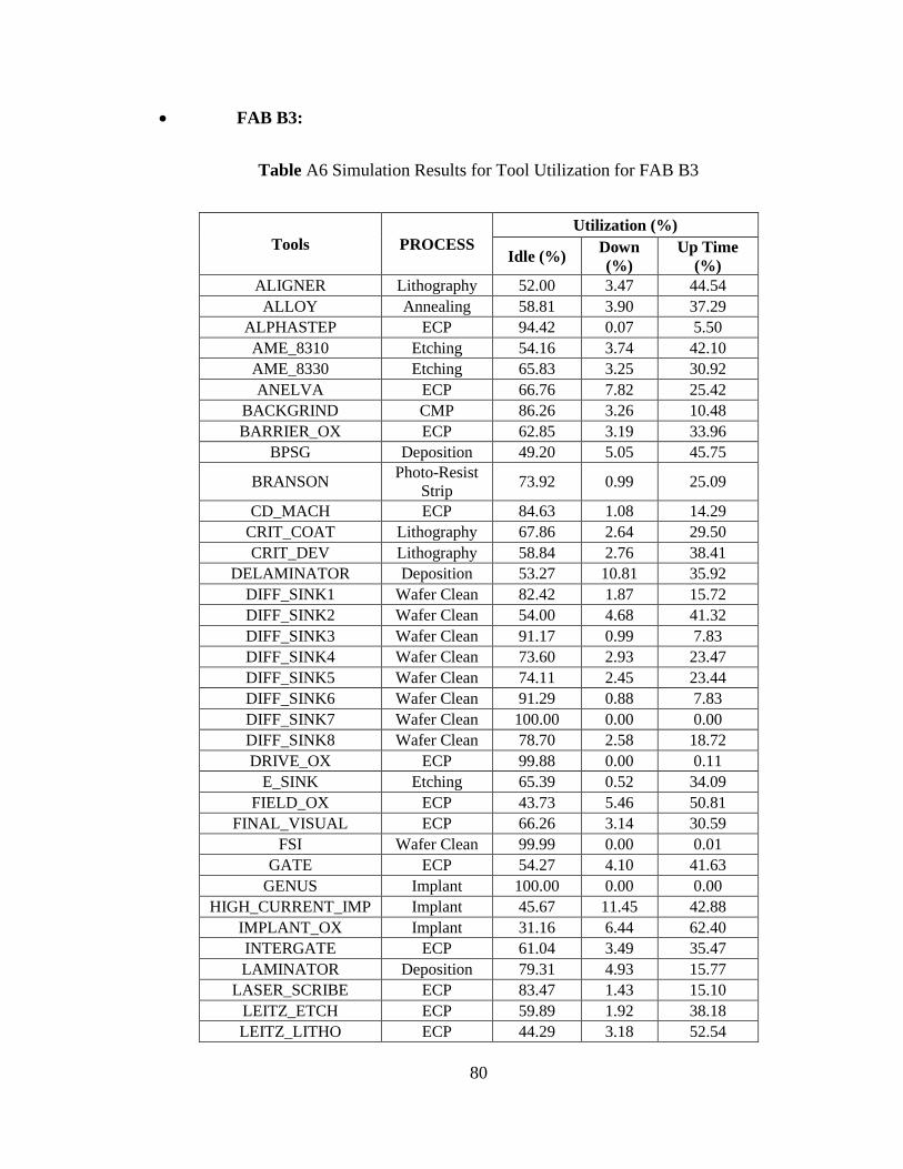
80
FAB B3:
Table A6 Simulation Results for Tool Utilization for FAB B3
Tools PROCESS
Utilization (%)
Idle (%) Down
(%)
Up Time
(%)
ALIGNER Lithography 52.00 3.47 44.54
ALLOY Annealing 58.81 3.90 37.29
ALPHASTEP ECP 94.42 0.07 5.50
AME_8310 Etching 54.16 3.74 42.10
AME_8330 Etching 65.83 3.25 30.92
ANELVA ECP 66.76 7.82 25.42
BACKGRIND CMP 86.26 3.26 10.48
BARRIER_OX ECP 62.85 3.19 33.96
BPSG Deposition 49.20 5.05 45.75
BRANSON Photo-Resist
Strip 73.92 0.99 25.09
CD_MACH ECP 84.63 1.08 14.29
CRIT_COAT Lithography 67.86 2.64 29.50
CRIT_DEV Lithography 58.84 2.76 38.41
DELAMINATOR Deposition 53.27 10.81 35.92
DIFF_SINK1 Wafer Clean 82.42 1.87 15.72
DIFF_SINK2 Wafer Clean 54.00 4.68 41.32
DIFF_SINK3 Wafer Clean 91.17 0.99 7.83
DIFF_SINK4 Wafer Clean 73.60 2.93 23.47
DIFF_SINK5 Wafer Clean 74.11 2.45 23.44
DIFF_SINK6 Wafer Clean 91.29 0.88 7.83
DIFF_SINK7 Wafer Clean 100.00 0.00 0.00
DIFF_SINK8 Wafer Clean 78.70 2.58 18.72
DRIVE_OX ECP 99.88 0.00 0.11
E_SINK Etching 65.39 0.52 34.09
FIELD_OX ECP 43.73 5.46 50.81
FINAL_VISUAL ECP 66.26 3.14 30.59
FSI Wafer Clean 99.99 0.00 0.01
GATE ECP 54.27 4.10 41.63
GENUS Implant 100.00 0.00 0.00
HIGH_CURRENT_IMP Implant 45.67 11.45 42.88
IMPLANT_OX Implant 31.16 6.44 62.40
INTERGATE ECP 61.04 3.49 35.47
LAMINATOR Deposition 79.31 4.93 15.77
LASER_SCRIBE ECP 83.47 1.43 15.10
LEITZ_ETCH ECP 59.89 1.92 38.18
LEITZ_LITHO ECP 44.29 3.18 52.54

81
Tools PROCESS
Utilization (%)
Idle (%) Down
(%)
Up Time
(%)
LTO Deposition 37.35 5.83 56.82
MATRIX Etching 57.51 2.26 40.24
MED_CURRENT_IMP Implant 46.36 11.76 41.88
METAL_SINK Wafer Clean 96.34 0.02 3.64
NANOSPEC ECP 97.92 0.24 1.84
NITRIDE ECP 99.98 0.00 0.02
NONCRIT_COAT Lithography 71.02 2.50 26.47
NONCRIT_DEV Lithography 56.06 4.54 39.40
OXIDE_1 Deposition 45.72 3.02 51.25
OXIDE_LAM Etching 20.14 8.60 71.26
PEAK ECP 91.81 0.62 7.57
POLY_DEP ECP 63.56 4.44 32.00
POLY_DOPE Implant 45.07 5.42 49.52
POLY_LAM Etching 36.73 5.35 57.92
PROMETRIX ECP 71.70 2.14 26.16
QUAESTAR ECP 100.00 0.00 0.00
RAINBOW_4500 Etching 58.04 2.86 39.11
REFLOW Annealing 99.99 0.00 0.01
SECOND_MASK Lithography 38.41 4.74 56.85
SILICIDE_TOOL Deposition 69.64 2.17 28.18
SINK_22_BOE Wafer Clean 100.00 0.00 0.00
SINK_22_CAROS Wafer Clean 59.51 0.55 39.94
SINK_24_BOE Wafer Clean 67.45 0.40 32.15
SINK_24_CAROS Wafer Clean 49.68 0.86 49.46
STEPPER Lithography 61.73 0.49 37.78
STRIPPER Photo-Resist
Strip 29.73 10.49 59.78
ULTRASONIC_CLEAN Wafer Clean 100.00 0.00 0.00
ULTRASONIC_TOOL Wafer Clean 93.62 0.66 5.72
UV_BAKE Annealing 97.92 0.01 2.07
UV_BAKE_BACKEND Annealing 63.73 2.49 33.77
VAPOR_PRIME_OVEN Lithography 71.11 1.77 27.12
VARIAN Implant 55.51 2.94 41.55
VWR_OVEN Annealing 64.24 10.36 25.39
WET_PROBE ECP 46.26 0.99 52.75
NEW_STEPPER Lithography 59.93 3.51 36.56

82
FAB C1:
Table A7 Simulation Results for Tool Utilization for FAB C1
Tools PROCESS
Utilization (%)
Idle (%) Down
(%) Up Time (%)
ALIGNER Lithography 58.54 3.12 38.35
ALLOY Annealing 65.22 3.12 31.67
ALPHASTEP ECP 98.58 0.01 1.41
AME_8310 Etching 56.85 3.60 39.55
AME_8330 Etching 67.87 3.07 29.06
ANELVA ECP 68.31 7.51 24.18
BACKGRIND CMP 87.08 3.07 9.85
BARRIER_OX ECP 30.83 6.16 63.02
BPSG Deposition 48.50 5.11 46.39
BRANSON Photo-Resist
Strip 93.40 0.31 6.29
CD_MACH ECP 86.65 1.06 12.28
CRIT_COAT Lithography 57.36 3.44 39.19
CRIT_DEV Lithography 45.03 3.68 51.29
DELAMINATOR Deposition 56.12 10.15 33.73
DIFF_SINK1 Wafer Clean 82.08 1.87 16.05
DIFF_SINK2 Wafer Clean 47.21 5.26 47.53
DIFF_SINK3 Wafer Clean 91.17 0.99 7.84
DIFF_SINK4 Wafer Clean 73.88 2.91 23.21
DIFF_SINK5 Wafer Clean 74.92 2.36 22.72
DIFF_SINK6 Wafer Clean 84.70 1.81 13.50
DIFF_SINK7 Wafer Clean 95.15 0.37 4.48
DIFF_SINK8 Wafer Clean 79.52 2.53 17.94
DRIVE_OX ECP 38.63 6.59 54.78
E_SINK Etching 41.99 0.68 57.32
FIELD_OX ECP 85.25 1.14 13.60
FINAL_VISUAL ECP 68.45 2.81 28.73
FSI Wafer Clean 47.75 9.09 43.16
GATE ECP 62.89 2.86 34.25
GENUS Implant 58.98 13.47 27.55
HIGH_CURRENT_IMP Implant 35.65 13.50 50.85
IMPLANT_OX Implant 33.43 6.02 60.55
INTERGATE ECP 20.65 7.31 72.04
LAMINATOR Deposition 80.41 4.78 14.82
LASER_SCRIBE ECP 82.79 1.48 15.72
LEITZ_ETCH ECP 41.15 2.94 55.90

83
Tools PROCESS
Utilization (%)
Idle (%) Down
(%) Up Time (%)
LEITZ_LITHO ECP 39.85 3.38 56.77
LTO Deposition 28.71 6.90 64.39
MATRIX Etching 50.34 2.68 46.98
MED_CURRENT_IMP Implant 26.91 15.57 57.51
METAL_SINK Wafer Clean 96.51 0.02 3.47
NANOSPEC ECP 89.42 1.45 9.13
NITRIDE ECP 99.98 0.00 0.02
NONCRIT_COAT Lithography 40.01 4.97 55.02
NONCRIT_DEV Lithography 62.33 3.85 33.82
OXIDE_1 Deposition 53.39 2.61 44.00
OXIDE_LAM Etching 68.65 3.30 28.05
PEAK ECP 84.95 1.10 13.95
POLY_DEP ECP 65.30 4.30 30.40
POLY_DOPE Implant 26.58 6.87 66.55
POLY_LAM Etching 43.03 4.58 52.39
PROMETRIX ECP 67.32 2.50 30.18
QUAESTAR ECP 79.72 4.97 15.31
RAINBOW_4500 Etching 65.16 2.50 32.33
REFLOW Annealing 56.13 3.55 40.31
SECOND_MASK Lithography 46.79 3.82 49.39
SILICIDE_TOOL Deposition 58.67 3.49 37.85
SINK_22_BOE Wafer Clean 99.48 0.01 0.51
SINK_22_CAROS Wafer Clean 64.64 0.41 34.95
SINK_24_BOE Wafer Clean 61.71 0.55 37.74
SINK_24_CAROS Wafer Clean 72.67 0.54 26.80
STEPPER Lithography 64.81 0.49 34.69
STRIPPER Photo-Resist
Strip 0.52 14.64 84.84
ULTRASONIC_CLEAN Wafer Clean 100.00 0.00 0.00
ULTRASONIC_TOOL Wafer Clean 94.00 0.63 5.37
UV_BAKE Annealing 98.04 0.01 1.95
UV_BAKE_BACKEND Annealing 65.02 2.40 32.58
VAPOR_PRIME_OVEN Lithography 72.85 1.68 25.47
VARIAN Implant 52.18 3.14 44.68
VWR_OVEN Annealing 65.86 9.99 24.16
WET_PROBE ECP 68.02 0.71 31.27
NEW_STEPPER Lithography 62.34 3.32 34.33

84
FAB C2:
Table A8 Simulation Results for Tool Utilization for FAB C2
Tools PROCESS Utilization (%)
Idle (%) Down (%) Up Time (%)
ALIGNER Lithography 53.24 3.64 43.12
ALLOY Annealing 60.03 3.56 36.41
ALPHASTEP ECP 97.12 0.01 2.87
AME_8310 Etching 52.32 3.92 43.75
AME_8330 Etching 64.45 3.42 32.13
ANELVA ECP 65.53 8.05 26.43
BACKGRIND CMP 85.70 3.40 10.90
BARRIER_OX ECP 38.30 5.40 56.30
BPSG Deposition 44.88 5.40 49.72
BRANSON Photo-Resist
Strip 86.32 0.60 13.08
CD_MACH ECP 85.52 1.09 13.39
CRIT_COAT Lithography 59.18 3.23 37.59
CRIT_DEV Lithography 46.95 3.55 49.50
DELAMINATOR Deposition 51.48 11.18 37.34
DIFF_SINK1 Wafer Clean 81.75 1.87 16.38
DIFF_SINK2 Wafer Clean 48.10 5.25 46.66
DIFF_SINK3 Wafer Clean 90.84 0.99 8.16
DIFF_SINK4 Wafer Clean 72.44 3.10 24.46
DIFF_SINK5 Wafer Clean 72.90 2.68 24.42
DIFF_SINK6 Wafer Clean 86.27 1.50 12.24
DIFF_SINK7 Wafer Clean 96.40 0.34 3.26
DIFF_SINK8 Wafer Clean 77.85 2.67 19.48
DRIVE_OX ECP 57.13 4.56 38.32
E_SINK Etching 48.34 0.64 51.01
FIELD_OX ECP 69.33 2.68 28.00
FINAL_VISUAL ECP 64.97 3.22 31.80
FSI Wafer Clean 62.46 7.46 30.08
GATE ECP 58.50 3.46 38.03
GENUS Implant 71.64 9.54 18.82
HIGH_CURRENT_IMP Implant 34.86 13.68 51.45
IMPLANT_OX Implant 29.32 6.49 64.19
INTERGATE ECP 27.92 6.71 65.37
LAMINATOR Deposition 78.41 5.21 16.39
LASER_SCRIBE ECP 82.77 1.48 15.75
LEITZ_ETCH ECP 44.06 2.81 53.13
LEITZ_LITHO ECP 37.94 3.44 58.62
LTO Deposition 27.08 6.91 66.01
MATRIX Etching 49.14 2.74 48.11
MED_CURRENT_IMP Implant 29.83 15.04 55.13
METAL_SINK Wafer Clean 96.19 0.02 3.79

85
Tools PROCESS Utilization (%)
Idle (%) Down (%) Up Time (%)
NANOSPEC ECP 91.69 1.23 7.08
NITRIDE ECP 99.98 0.00 0.02
NONCRIT_COAT Lithography 47.55 4.32 48.13
NONCRIT_DEV Lithography 57.57 4.37 38.06
OXIDE_1 Deposition 47.57 2.92 49.50
OXIDE_LAM Etching 46.59 5.69 47.71
PEAK ECP 86.41 0.96 12.63
POLY_DEP ECP 62.18 4.59 33.24
POLY_DOPE Implant 29.19 6.69 64.12
POLY_LAM Etching 38.73 5.09 56.18
PROMETRIX ECP 67.24 2.50 30.26
QUAESTAR ECP 85.42 3.71 10.88
RAINBOW_4500 Etching 60.66 2.67 36.66
REFLOW Annealing 67.75 2.66 29.58
SECOND_MASK Lithography 40.25 4.34 55.40
SILICIDE_TOOL Deposition 60.33 3.21 36.46
SINK_22_BOE Wafer Clean 99.67 0.01 0.32
SINK_22_CAROS Wafer Clean 60.25 0.46 39.29
SINK_24_BOE Wafer Clean 60.93 0.55 38.51
SINK_24_CAROS Wafer Clean 63.03 0.66 36.31
STEPPER Lithography 61.81 0.51 37.69
STRIPPER Photo-Resist
Strip 5.48 13.90 80.61
ULTRASONIC_CLEAN Wafer Clean 100.00 0.00 0.00
ULTRASONIC_TOOL Wafer Clean 93.38 0.67 5.95
UV_BAKE Annealing 97.84 0.01 2.16
UV_BAKE_BACKEND Annealing 62.08 2.66 35.25
VAPOR_PRIME_OVEN Lithography 69.98 1.83 28.20
VARIAN Implant 50.83 3.17 46.00
VWR_OVEN Annealing 62.62 10.98 26.39
WET_PROBE ECP 58.11 0.83 41.05
NEW_STEPPER Lithography 58.36 3.63 38.00

86
FAB C3:
Table A9 Simulation Results for Tool Utilization for FAB C3
Tools PROCESS
Utilization (%)
Idle
(%) Down (%) Up Time (%)
ALIGNER Lithography 49.24 3.83 46.93
ALLOY Annealing 56.60 4.04 39.36
ALPHASTEP ECP 94.11 0.09 5.80
AME_8310 Etching 51.63 4.02 44.36
AME_8330 Etching 63.96 3.46 32.58
ANELVA ECP 65.13 8.08 26.79
BACKGRIND CMP 85.54 3.41 11.05
BARRIER_OX ECP 61.12 3.29 35.59
BPSG Deposition 46.90 5.23 47.87
BRANSON Photo-Resist
Strip 72.45 1.04 26.51
CD_MACH ECP 84.03 1.09 14.88
CRIT_COAT Lithography 66.18 2.72 31.10
CRIT_DEV Lithography 56.63 2.88 40.48
DELAMINATOR Deposition 50.89 11.25 37.87
DIFF_SINK1 Wafer Clean 81.56 1.87 16.57
DIFF_SINK2 Wafer Clean 51.53 4.94 43.53
DIFF_SINK3 Wafer Clean 90.75 0.99 8.25
DIFF_SINK4 Wafer Clean 72.16 3.10 24.74
DIFF_SINK5 Wafer Clean 72.61 2.69 24.70
DIFF_SINK6 Wafer Clean 90.79 0.96 8.25
DIFF_SINK7 Wafer Clean 100.00 0.00 0.00
DIFF_SINK8 Wafer Clean 77.60 2.67 19.73
DRIVE_OX ECP 99.88 0.00 0.11
E_SINK Etching 63.34 0.54 36.12
FIELD_OX ECP 41.26 5.65 53.08
FINAL_VISUAL ECP 64.48 3.27 32.25
FSI Wafer Clean 99.99 0.00 0.01
GATE ECP 52.34 4.25 43.40
GENUS Implant 100.00 0.00 0.00
HIGH_CURRENT_IMP Implant 42.87 12.00 45.13
IMPLANT_OX Implant 28.77 6.60 64.63
INTERGATE ECP 59.03 3.75 37.22
LAMINATOR Deposition 78.14 5.24 16.62
LASER_SCRIBE ECP 82.58 1.50 15.92
LEITZ_ETCH ECP 57.71 2.05 40.24
LEITZ_LITHO ECP 41.33 3.30 55.37

87
Tools PROCESS
Utilization (%)
Idle
(%) Down (%) Up Time (%)
LTO Deposition 34.77 6.08 59.14
MATRIX Etching 55.16 2.42 42.41
MED_CURRENT_IMP Implant 43.64 12.44 43.91
METAL_SINK Wafer Clean 96.14 0.02 3.84
NANOSPEC ECP 97.61 0.45 1.93
NITRIDE ECP 99.98 0.00 0.02
NONCRIT_COAT Lithography 69.54 2.64 27.82
NONCRIT_DEV Lithography 53.73 4.75 41.52
OXIDE_1 Deposition 42.81 3.18 54.01
OXIDE_LAM Etching 17.75 8.84 73.41
PEAK ECP 91.36 0.66 7.98
POLY_DEP ECP 61.62 4.65 33.73
POLY_DOPE Implant 42.43 5.66 51.92
POLY_LAM Etching 34.07 5.58 60.35
PROMETRIX ECP 70.16 2.27 27.57
QUAESTAR ECP 100.00 0.00 0.00
RAINBOW_4500 Etching 55.81 2.98 41.21
REFLOW Annealing 100.00 0.00 0.00
SECOND_MASK Lithography 36.02 4.85 59.12
SILICIDE_TOOL Deposition 68.14 2.25 29.61
SINK_22_BOE Wafer Clean 100.00 0.00 0.00
SINK_22_CAROS Wafer Clean 57.18 0.57 42.25
SINK_24_BOE Wafer Clean 65.34 0.42 34.24
SINK_24_CAROS Wafer Clean 46.18 0.89 52.93
STEPPER Lithography 58.81 0.51 40.69
STRIPPER Photo-Resist
Strip 26.04 10.95 63.00
ULTRASONIC_CLEAN Wafer Clean 100.00 0.00 0.00
ULTRASONIC_TOOL Wafer Clean 93.30 0.67 6.03
UV_BAKE Annealing 97.81 0.01 2.19
UV_BAKE_BACKEND Annealing 61.59 2.74 35.67
VAPOR_PRIME_OVEN Lithography 69.56 1.84 28.60
VARIAN Implant 53.13 3.08 43.79
VWR_OVEN Annealing 62.08 11.16 26.76
WET_PROBE ECP 43.27 1.06 55.67
NEW_STEPPER Lithography 57.71 3.75 38.54

88
REFERENCES
[1] Semiconductor sales revenue worldwide from 1987 to 2019 (in billion U.S. dollars)
<https://www.statista.com/statistics/266973/global-semiconductor-sales-since-
1988/>
[2] Villarreal, S., Jimenez, J. A., Jin, T., & Cabrera-Rios, M. (2013). Designing a
sustainable and distributed generation system for semiconductor wafer fabs. IEEE
Transactions on Automation Science and Engineering, 10(1), 16-26.
[3] L. Freris and D. Infield, Renewable Energy in Power System, 1st ed. New York: Wiley,
2008.
[4] Jimenez, J. A., Mackulak, G. T., & Fowler, J. W. (2008). Levels of capacity and
material handling system modeling for factory integration decision making in
semiconductor wafer fabs. IEEE Transactions on Semiconductor Manufacturing,
21(4), 600-613.
[5] Jimenez, J. (2018). Modeling and Analysis of Semiconductor Green Wafer Fabs.
[6] Ziarnetzky, T., Mönch, L., Kannaian, T., & Jimenez, J. (2017, December).
Incorporating elements of a sustainable and distributed generation system into a
production planning model for a wafer fab. In Simulation Conference (WSC), 2017
Winter (pp. 3519-3530). IEEE.
[7] International Technology Roadmap of Semiconductors, Environmental, Safety and
Health Chapter 2011. [Online]. Available: http://www.itrs.net
[8] S. Hu and Y. Chuah, “Power consumption of semiconductor fabs in Taiwan,” Energy,
vol. 28, no. 8, pp. 895–907, 2003.

89
[9] Hu, S. C., Wu, J. S., Chan, D. Y. L., Hsu, R. T. C., & Lee, J. C. C. (2008). Power
consumption benchmark for a semiconductor cleanroom facility system. Energy and
Buildings, 40(9), 1765-1770.
[10] Hu, S. C., Xu, T., Chaung, T., & Chan, D. Y. L. (2010). Characterization of energy
use in 300 mm DRAM (Dynamic Random Access Memory) wafer fabrication plants
(fabs) in Taiwan. Energy, 35(9), 3788-3792.
[11] Gallachóir, B. Ó., & Cahill, C. (2009). Modelling energy consumption in a
manufacturing plant using productivity KPIs. ECEEE Summer Study. Act! Innovate!
Deliver! Reducing Energy Demand Sustainably.
[12] Santana-Viera, V., Jimenez, J., Jin, T., & Espiritu, J. (2015). Implementing factory
demand response via onsite renewable energy: a design-of-experiment approach.
International Journal of Production Research, 53(23), 7034-7048.
[13] Chiang, C., Hsu, H. (2015). Incorporating pollution taxes and/or subsidies into master
planning in semiconductor foundry plants. Transactions on Semiconductor
Manufacturing, TSM-15-0016
[14] Rosendahl, K. E., & Strand, J. (2015). Emissions trading with offset markets and free
quota allocations. Environmental and Resource Economics, 61(2), 243-271.
[15] Tseng, S. C., & Hung, S. W. (2014). A strategic decision-making model considering
the social costs of carbon dioxide emissions for sustainable supply chain management.
Journal of environmental management, 133, 315-322.

90
[16] Jin, M., Granda-Marulanda, N. A., & Down, I. (2014). The impact of carbon policies
on supply chain design and logistics of a major retailer. Journal of Cleaner Production,
85, 453-461.
[17] Du, S. F., Dong, J. F., Liang, L., & Zhang, J. J. (2009). Optimal production policy
with emission permits and trading. Chinese Journal of management science, 17(3), 81-
86.
[18] He, P., Zhang, W., Xu, X., & Bian, Y. (2015). Production lot-sizing and carbon
emissions under cap-and-trade and carbon tax regulations. Journal of Cleaner
Production, 103, 241-248.
[19] Absi, N., Dauzère-Pérès, S., Kedad-Sidhoum, S., Penz, B., & Rapine, C. (2013). Lot
sizing with carbon emission constraints. European Journal of Operational Research,
227(1), 55-61.
[20] Chiang, C., & Hsu, H. L. (2017). Incorporating Pollution Taxes and/or Subsidies into
Master Planning in Semiconductor Foundry Plants. International Journal of
Management and Sustainability, 6(1), 8-22.
[21] Du, S., Tang, W., & Song, M. (2016). Low-carbon production with low-carbon
premium in cap-and-trade regulation. Journal of cleaner production, 134, 652-662.
[22] Benjaafar, S., Li, Y., & Daskin, M. (2013). Carbon footprint and the management of
supply chains: Insights from simple models. IEEE transactions on automation science
and engineering, 10(1), 99-116.

91
[23] Du, S., Ma, F., Fu, Z., Zhu, L., & Zhang, J. (2015). Game-theoretic analysis for an
emission-dependent supply chain in a ‘cap-and-trade’system. Annals of Operations
Research, 228(1), 135-149.
[24] Hou, Y., Jia, M., Tian, X., Wei, F., & Wei, K. (2015). Optimal decisions of countries
with carbon tax and carbon tariff. Journal of Industrial Engineering and Management,
8(3), 981-1001.
[25] Xu, X., Xu, X., & He, P. (2016). Joint production and pricing decisions for multiple
products with cap-and-trade and carbon tax regulations. Journal of Cleaner
Production, 112, 4093-4106.
[26] Liu, L. C., Liang, Q. M., & Wang, Q. (2015). Accounting for China's regional carbon
emissions in 2002 and 2007: production-based versus consumption-based principles.
Journal of Cleaner Production, 103, 384-392.
[27] Uzsoy, R., Lee, C. Y., & Martin-Vega, L. A. (1992). A review of production planning
and scheduling models in the semiconductor industry part I: system characteristics,
performance evaluation and production planning. IIE transactions, 24(4), 47-60.
[28] Karabuk, S., & Wu, S. D. (1999). Strategic capacity planning in the semiconductor
industry: A stochastic programming approach. Lehigh University, Department of
industrial and Manufacturing Systems Engineering, Report, (99T-12).
[29] Toktay, L. B., & Uzsoy, R. (1994). Capacity Allocation with Integer Side Constraints:
An Application in Semiconductor Manufacturing. School of Industrial Engineering,
Purdue University.

92
[30] Swaminathan, J. M. (2000). Tool capacity planning for semiconductor fabrication
facilities under demand uncertainty. European Journal of Operational Research,
120(3), 545-558.
[31] Liu, J., Yang, F., Wan, H., & Fowler, J. W. (2011). Capacity planning through
queueing analysis and simulation-based statistical methods: a case study for
semiconductor wafer fabs. International Journal of Production Research, 49(15),
4573-4591.
[32] Stray, J., Fowler, J., Carlyle, W., & Rastogi, A. (2006). Enterprise-Wide
Semiconductor Manufacturing Resource Planning. IEEE Transactions on
Semiconductor Manufacturing, 19(2), 259-268
[33] Yılmaz, P., & Çatay, B. (2006). Strategic level three-stage production distribution
planning with capacity expansion. Computers & Industrial Engineering, 51(4), 609-
620.
[34] Ziarnetzky, T., & Mönch, L. (2016, December). Simulation-based optimization for
integrated production planning and capacity expansion decisions. In Winter
Simulation Conference (WSC), 2016 (pp. 2992-3003). IEEE.
[35] Hung, Y. F., & Leachman, R. C. (1996). A production planning methodology for
semiconductor manufacturing based on iterative simulation and linear programming
calculations. IEEE Transactions on Semiconductor manufacturing, 9(2), 257-269.
[36] Raiborn, C. A., Joyner, B. E., & Logan, J. W. (1999). ISO 14000 and the Bottom Line.
Quality Progress, 32(11), 89.

93
[37] Rădulescu, M., Rădulescu, S., & Rădulescu, C. Z. (2009). Sustainable production
technologies which take into account environmental constraints. European Journal of
Operational Research, 193(3), 730-740.
[38] Pirila, P. (1994). Emission oriented production planning in the Finnish pulp and paper
industry. In Joint National Meeting TIMS/ORSA April (pp. 24-27).
[39] Tuma, A., & Haasis, H. D. (1994, January). Emission Oriented Production Planning
in Interconnected Production Systems Using Fuzzy Systems Neural Networks and
Neural Fuzzy Approaches. In ICONIP: International Conference On Neural
Information Processing (Vol. 3, No. 3, pp. 1813-1817).
[40] Golari, M., Fan, N., & Jin, T. (2017). Multistage Stochastic Optimization for
Production‐Inventory Planning with Intermittent Renewable Energy. Production and
Operations Management, 26(3), 409-425.
[41] Chaabane, A., & Geramianfar, R. (2015, May). Sustainable supply chain planning and
optimization trade-offs between cost, GHG emissions and service level. In Advanced
Logistics and Transport (ICALT), 2015 4th International Conference on (pp. 327-
332). IEEE.
[42] Zhang, B., & Xu, L. (2013). Multi-item production planning with carbon cap and trade
mechanism. International Journal of Production Economics, 144(1), 118-127.
[43] Helmrich, M. J. R., Jans, R., van den Heuvel, W., & Wagelmans, A. P. (2015). The
economic lot-sizing problem with an emission capacity constraint. European Journal
of Operational Research, 241(1), 50-62.

94
[44] Ross, M. (1992). Efficient energy use in manufacturing. Proceedings of the National
Academy of Sciences, 89(3), 827-831.
[45] Gallachóir, B. Ó., & Cahill, C. (2009). Modelling energy consumption in a
manufacturing plant using productivity KPIs. ECEEE Summer Study. Act! Innovate!
Deliver! Reducing Energy Demand Sustainably.
[46] Fowler, J., & Robinson, J. (1995). Measurement and improvement of manufacturing
capacities (MIMAC): Final report. Technical Report 95062861A-TR, SEMATECH,
Austin, TX.
[47] Krishnan N, Williams E, Boyd S. Secondary materialization: energy use to realize
ultra-high purities in semiconductor manufacturing. In: Proceedings of the 2008 IEEE
international symposium on electronics & the environment. Piscataway, New Jersey:
IEEE; 2008.
[48] Eccles, R. G., Perkins, K. M., & Serafeim, G. (2012). How to become a sustainable
company. MIT Sloan Management Review, 53(4), 43-50.
[49] Interconnect, E. E., Living, S., & Computing, G. (2008). Technology with the
Environment in Mind. Intel Technology Journal, 12(1).