carbon nanomaterials for next-generation interconnects · pdf filecarbon nanomaterials for...
TRANSCRIPT
IEEE TRANSACTIONS ON ELECTRON DEVICES, VOL. 56, NO. 9, SEPTEMBER 2009 1799
Carbon Nanomaterials for Next-GenerationInterconnects and Passives: Physics,
Status, and ProspectsHong Li, Student Member, IEEE, Chuan Xu, Student Member, IEEE, Navin Srivastava, Student Member, IEEE,
and Kaustav Banerjee, Senior Member, IEEE
(Invited Paper)
Abstract—This paper reviews the current state of researchin carbon-based nanomaterials, particularly the one-dimensional(1-D) forms, carbon nanotubes (CNTs) and graphene nanoribbons(GNRs), whose promising electrical, thermal, and mechanicalproperties make them attractive candidates for next-generationintegrated circuit (IC) applications. After summarizing the basicphysics of these materials, the state of the art of their interconnect-related fabrication and modeling efforts is reviewed. Both elec-trical and thermal modeling and performance analysis forvarious CNT- and GNR-based interconnects are presented andcompared with conventional interconnect materials to provideguidelines for their prospective applications. It is shown thatsingle-walled, double-walled, and multiwalled CNTs can providebetter performance than that of Cu. However, in order to makeGNR interconnects comparable with Cu or CNT interconnects,both intercalation doping and high edge-specularity must beachieved. Thermal analysis of CNTs shows significant advantagesin tall vias, indicating their promising application as through-silicon vias in 3-D ICs. In addition to on-chip interconnects,various applications exploiting the low-dimensional propertiesof these nanomaterials are discussed. These include chip-to-packaging interconnects as well as passive devices for future gener-ations of IC technology. Specifically, the small form factor of CNTsand reduced skin effect in CNT interconnects have significantimplications for the design of on-chip capacitors and inductors,respectively.
Index Terms—Capacitor, carbon nanomaterials, double-walledcarbon nanotube (CNT), energy storage, graphene nanoribbon(GNR), high-frequency, inductor, interconnects, multiwalled CNT,single-walled CNT, skin effect, through-silicon vias (TSVs).
Manuscript received February 18, 2009. Current version publishedAugust 21, 2009. This work was supported by the National Institute of Stan-dards and Technology under Grant 70NANB5H1215, and the National ScienceFoundation under Grant CCF-0811880 and Grant CCF-0917385. The review ofthis paper was arranged by Editor S. Saha.
H. Li, C. Xu, and K. Banerjee are with the Department of Electricaland Computer Engineering, University of California, Santa Barbara, CA93106 USA (e-mail: [email protected]; [email protected]; [email protected]).
N. Srivastava was with the Department of Electrical and Computer Engi-neering, University of California, Santa Barbara, CA 93106 USA. He is nowwith the Mentor Graphics Corporation, Wilsonville, OR 97070 USA (e-mail:[email protected]).
Color versions of one or more of the figures in this paper are available onlineat http://ieeexplore.ieee.org.
Digital Object Identifier 10.1109/TED.2009.2026524
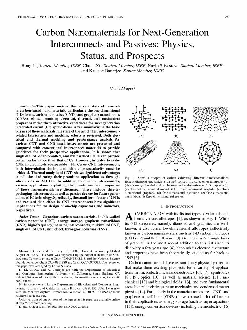
Fig. 1. Some allotropes of carbon exhibiting different dimensionalities.Except diamond (a), which is an sp3-bonded structure, other allotropes (b),(d)–(f) are sp2 bonded and can be regarded as derivatives of 2-D graphene (c).(a) Three-dimensional diamond. (b) Three-dimensional graphite. (c) Two-dimensional graphene. (d) One-dimensional nanotube. (e) One-dimensionalnanoribbon. (f) Zero-dimensional fullerenes.
I. INTRODUCTION
A CARBON ATOM with its distinct types of valence bondsforms various allotropes [1], as shown in Fig. 1. While
its 3-D structures, namely, diamond and graphite, are well-known, it also forms low-dimensional allotropes collectivelyknown as carbon nanomaterials, such as 1-D carbon nanotubes(CNTs) [2] and 0-D fullerenes [3]. Graphene, a 2-D single layerof graphite, is the most recent addition to this list since itsdiscovery a few years ago [4], although its electronic structureand properties have been theoretically studied as far back as1947 [5].
Carbon nanomaterials have extraordinary physical propertiesthat make them exciting prospects for a variety of applica-tions in microelectronics/nanoelectronics [6], [7], spintronics[8], [9], optics [10], as well as material science [11], me-chanical [12] and biological fields [13], and even fundamentalareas like relativistic quantum mechanics and condensed matterphysics [14]. Particularly in the nanoelectronics area, CNTs andgraphene nanoribbons (GNRs) have aroused a lot of interestin their applications as energy storage (such as supercapacitors[15]), energy conversion devices (including thermoelectric [16]
0018-9383/$26.00 © 2009 IEEE
Authorized licensed use limited to: Univ of California-Santa Barbara. Downloaded on August 28, 2009 at 16:06 from IEEE Xplore. Restrictions apply.
1800 IEEE TRANSACTIONS ON ELECTRON DEVICES, VOL. 56, NO. 9, SEPTEMBER 2009
TABLE IPROPERTIES OF CARBON NANOMATERIALS RELEVANT TO VLSI
INTERCONNECTS AND PASSIVES
and photovoltaic [17] devices), field emission displays andradiation sources [18], nanometer semiconductor transistors[4], [19]–[22], nanoelectromechanical systems (NEMS) [23],[24], electrostatic discharge (ESD) protection [25], as well asinterconnects [26]–[29] and passives [30], [31], due to theirextraordinary electrical, thermal, and mechanical properties [4],[12], [32]–[46]. A summary of the key properties of carbonnanomaterials relevant to this paper is provided in Table I. Thesp2 bonding in these materials, which is stronger than the sp3
bonds in diamond, makes graphene the strongest material evermeasured [47]. The properties of graphite, which is also ansp2-bonded structure, provide first hints toward the remarkableproperties of CNTs and GNRs. The charge carrier densities ingraphite are almost equal for electrons and holes (ne ≈ nh ≈7 × 10¹⁸/cm3) and measured mobilities are on the order of104 cm2/V · s at room temperature and 106 cm2/V · s at 4.2 K[48]. Graphene and CNTs also have very high current carryingcapability (at least two orders of magnitude higher than that ofCu) [4], [32], [33]. In addition, CNT and GNR are found to havelong mean free paths (MFPs) at low bias due to weak acousticphonon scattering and suppressed optical phonon scattering atroom temperature [43], [49]. Unlike the scattering mechanismsin a 3-D conductor, where scattering can occur at small anglesand the required momentum is relatively low, the backscattering(180◦ angle) in 1-D conductor requires much higher momentumand thus the scattering is weak, leading to larger momentumrelaxation time or mean free path. All of these unique propertiesindicate that CNT and GNR could be potentially employedas alternative materials for next-generation nanoscale intercon-nects, which can enhance the electrical performance as wellas eliminate electromigration reliability concerns that plaguenanoscale Cu interconnects [50], [51].
As reliability concerns put a question mark on the continueduse of Cu (due to increasing resistivity, current density, and on-chip metal temperatures) at the nanoscale [52]–[54], this paperprovides a comprehensive review of the physics of these carbonnanomaterials, current status of their fabrication and modeling,and their prospects for replacing standard interconnect metalsin applications ranging from on-chip interconnections to energystorage and packaging elements for integrated circuit (IC)applications. It provides an overview of the state of the art ofCNT and GNR interconnect-related fabrication and modeling
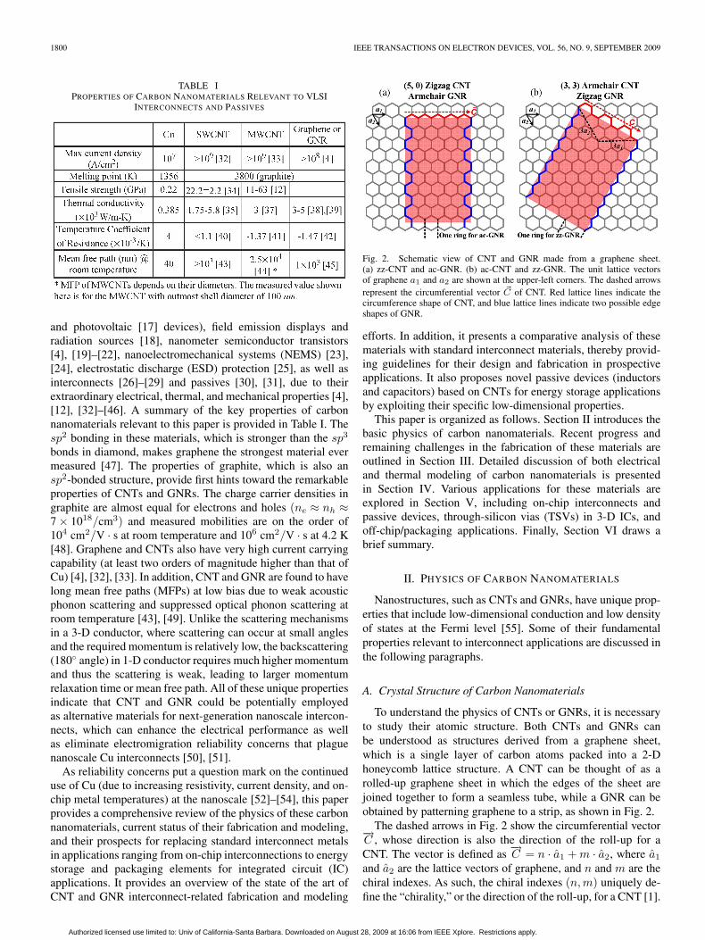
Fig. 2. Schematic view of CNT and GNR made from a graphene sheet.(a) zz-CNT and ac-GNR. (b) ac-CNT and zz-GNR. The unit lattice vectorsof graphene a1 and a2 are shown at the upper-left corners. The dashed arrowsrepresent the circumferential vector �C of CNT. Red lattice lines indicate thecircumference shape of CNT, and blue lattice lines indicate two possible edgeshapes of GNR.
efforts. In addition, it presents a comparative analysis of thesematerials with standard interconnect materials, thereby provid-ing guidelines for their design and fabrication in prospectiveapplications. It also proposes novel passive devices (inductorsand capacitors) based on CNTs for energy storage applicationsby exploiting their specific low-dimensional properties.
This paper is organized as follows. Section II introduces thebasic physics of carbon nanomaterials. Recent progress andremaining challenges in the fabrication of these materials areoutlined in Section III. Detailed discussion of both electricaland thermal modeling of carbon nanomaterials is presentedin Section IV. Various applications for these materials areexplored in Section V, including on-chip interconnects andpassive devices, through-silicon vias (TSVs) in 3-D ICs, andoff-chip/packaging applications. Finally, Section VI draws abrief summary.
II. PHYSICS OF CARBON NANOMATERIALS
Nanostructures, such as CNTs and GNRs, have unique prop-erties that include low-dimensional conduction and low densityof states at the Fermi level [55]. Some of their fundamentalproperties relevant to interconnect applications are discussed inthe following paragraphs.
A. Crystal Structure of Carbon Nanomaterials
To understand the physics of CNTs or GNRs, it is necessaryto study their atomic structure. Both CNTs and GNRs canbe understood as structures derived from a graphene sheet,which is a single layer of carbon atoms packed into a 2-Dhoneycomb lattice structure. A CNT can be thought of as arolled-up graphene sheet in which the edges of the sheet arejoined together to form a seamless tube, while a GNR can beobtained by patterning graphene to a strip, as shown in Fig. 2.
The dashed arrows in Fig. 2 show the circumferential vector−→C , whose direction is also the direction of the roll-up for aCNT. The vector is defined as
−→C = n · a1 + m · a2, where a1
and a2 are the lattice vectors of graphene, and n and m are thechiral indexes. As such, the chiral indexes (n,m) uniquely de-fine the “chirality,” or the direction of the roll-up, for a CNT [1].
Authorized licensed use limited to: Univ of California-Santa Barbara. Downloaded on August 28, 2009 at 16:06 from IEEE Xplore. Restrictions apply.

LI et al.: CARBON NANOMATERIALS FOR NEXT-GENERATION INTERCONNECTS AND PASSIVES 1801
Fig. 3. (a) Band structure of graphene forms hexagonal cones in the vicinityof the Fermi energy. The apexes of the six cones are called Dirac points. Theformation of a nanotube cuts the energy landscape into slices of allowed states(wave vector is quantized). The locations of the cross section of the cut linesin k-space with the cones determine whether the resulting band structure is(b) metallic or (c) semiconducting.
The length of C is the circumference of CNT, from which itsdiameter D can be calculated as follows:
D = |−→C |/π =a
π
√n2 + m2 + mn (1)
where a is the lattice constant of graphene (= 0.246 nm). InFig. 2(a), the circumferential vector
−→C = 5 a1 + 0 a2, hence,
the CNT rolled up along−→C is identified as (5, 0). In this
case, because the circumferential edge of CNT has a zigzagshape (shown in red), it is also called a zigzag CNT (zz-CNT).Similarly, for the case shown in Fig. 2(b), the CNT is identifiedwith the chiral indexes (3, 3), and because the circumferentialedge of the CNT has armchair shape, it is called an armchairCNT (ac-CNT). All zz-CNTs have indexes n or m = 0, whileac-CNTs have n = m. The two cases shown in Fig. 2 arespecial cases where the circumferential vector of CNT is eitheralong the lattice vectors (n or m = 0) or along the exactdirection between two vectors (n = m). For other directionsof circumferential vector, the CNTs are called “chiral.”
The chirality of a GNR, on the other hand, is defined by theedge shape as shown in Fig. 2 (in blue), which is perpendicularto the circumferential vector for a CNT. As a result, the GNR(shaded) in Fig. 2(a) is armchair, while the one in Fig. 2(b) iszigzag.
B. Electrical Properties
The band structure of graphene is the basis for understandingthe electronic behavior of CNTs and GNRs. The Brillouin zoneof graphene is shown in Fig. 3(a), where the cones representthe electron energy dispersion of graphene close to the Fermienergy. It can be calculated by a simple tight-binding approach[1]. The band structure of graphene is unique in the sense thatthe E−k relation is linear for lowest energies near the sixcorners of the 2-D hexagonal Brillouin zone, leading to zeroeffective mass for electrons and holes [56] (for more details, seethe Appendix I). Due to this linear “dispersion” relation at lowenergies, electrons and holes near these six points behave likerelativistic particles described by the Dirac equation for spin1/2 particles [6]. Hence, the electrons and holes are called Diracfermions, and the six corners of the Brillouin zone [the apexesof the six cones shown in Fig. 3(a)] are called the Dirac points.
Since a CNT can be regarded as a seamless rolled-upgraphene sheet, it has periodic boundary conditions around thecircumference. This periodicity requires that the wave vector
Fig. 4. Band structures of (a) ac-CNT (n = m = 20, D = 2.7 nm) and(b) zz-GNR (N = 26, w = 11 nm), where N is the number of hexagonalcarbon rings across the width of GNR, w is the width of GNR, and a is thelattice constant.
along the circumference be quantized as |−→C | = iλ or−→C · −→k =
2π · i, where i is a nonzero integer, and λ is the electron wavelength. The quantization condition is reflected in the Brillouinzone as slices cut out of the band structure, indicated by thesolid lines in Fig. 3(a). The separation between the slices is2π/|−→C | = 2/D, and their orientation depends on the nanotube“chirality” or index (n, m) [55]. For a specific tube diameter andchirality, if there is a slice cut exactly at the apex of the cones[as in Fig. 3(a)], there is no bandgap between the conductionand valence bands, as shown in Fig. 3(b). Such nanotubes aremetallic. If the slices cut elsewhere on the cones, there willbe a bandgap around the Fermi energy, as shown in Fig. 3(c),and such nanotubes are semiconducting. The condition forachieving metallic tubes is expressed as n − m = 3i, where iis an integer [1] (for more details, see Appendix II). Hence,ac-CNTs are always metallic [see the bandstructure shown inFig. 4(a)], while zz-CNTs could be metallic or semiconducting,depending on the chiral indexes (n, m). For a natural mix ofCNTs, statistically, one-third of the CNTs are metallic, and theother two-thirds are semiconducting [1]. Since the spacing ofslices is inversely proportional to D, larger-diameter nanotubeshave more slices with smaller spacing between slices, whichleads to smaller bandgaps for semiconducting CNTs.
Although GNRs are also derivatives of graphene, the dif-ference between CNTs and GNRs arises from the boundarycondition: the wave function along the CNT circumferenceis periodic, while the wave function along the GNR widthvanishes at the two edges. Thus, the wave vector quantizationin GNR is w = i · λ/2 or w · −→k = π · i, where w is the widthof GNR, and i is an integer. Armchair GNRs (ac-GNRs) canbe either metallic or semiconducting, depending on the num-ber (N) of hexagonal carbon rings (shown in Fig. 2) acrossthe width: metallic when N = 3i − 1 (the transverse wavevector with respect to the Dirac point, Δktransverse = nπ/w,where n is an integer; for n = 0, Δktransverse = 0, imply-ing that the zeroth subbands pass through the Dirac points),and semiconducting when N =3i or 3i+1 (Δktransverse =(n+1/3)π/w or Δktransverse =(n−1/3)π/w), where i is aninteger. In comparison, zigzag GNRs (zz-GNRs) are alwaysmetallic and independent of N . While the band structure ofac-GNRs are similar to that of zz-CNTs, the electronic statesof zz-GNRs are more complicated than those of ac-CNTs.Particularly, the zz-GNRs have the “dispersionless band” or“zero mode,” which originates from the edge states [57], [58]:
Authorized licensed use limited to: Univ of California-Santa Barbara. Downloaded on August 28, 2009 at 16:06 from IEEE Xplore. Restrictions apply.

1802 IEEE TRANSACTIONS ON ELECTRON DEVICES, VOL. 56, NO. 9, SEPTEMBER 2009
TABLE IICONDITIONS OF METALLICITY FOR CNT AND GNR (n, m IS THE
CHIRALITY INDEX OF CNT, N IS THE NUMBER OF HEXAGONAL
CARBON RINGS, AND i IS AN INTEGER)
almost flatband appears within the region of 2π/3 < |ka| ≤ π[shown in Fig. 4(b)]. According to the band structure, zz-GNRsare always metallic. However, when wire width is smaller than10 nm, neutral zz-GNRs will have small bandgap because ofthe staggered sublattice potential from magnetic ordering onceelectron spin is considered [19], [59]. The bandgap of zz-GNRsincreases with decreasing wire width (the bandgap, in electron-volts, is 0.933/(w + 1.5), with w in nanometers).
Since the focus in this paper is on the metallicity of CNTsor GNRs, Table II summarizes the conditions of metallicity forboth CNTs and GNRs.
C. Heat Transport Properties
The measured high thermal conductivity of CNTs [35]–[37] and GNRs [38], [39] is higher than that of diamond(∼2000 W/m · K). It is important to understand the heat trans-port mechanism in CNTs/GNRs to get an insight into theiroutstanding thermal properties. Since the following analysiswill be valid for both CNTs and GNRs, we will only discussthe case of CNTs.
One important heat transport property of CNT (due to itslow dimensionality) is the quantization of thermal conduc-tance, which is theoretically analyzed in [60]. The quantum ofthermal conductance Gth
0 , is Gth0 = π2k2
BT/3h, where kB isBoltzmann’s constant, T is the temperature, and h is Planck’sconstant. Recently, quantization of thermal conductance ofCNT has been observed experimentally for individual CNTs[61] and agrees well with the theoretical prediction [62].
Another important heat transport property is that phononsdominate the heat conduction in CNTs, unlike electrons in tra-ditional metals. According to the simultaneous measurement ofthermal conductivity κ and electrical conductivity σ of SWCNTwith a diameter of 1.4 nm, the measured value of κ/σT istwo orders of magnitude larger than the Lorentz number 2.45 ×10⁻⁸ W · Ω/K2 [35]. This implies that the electron contributionto heat transport is very small, and that Wiedemann–Franz law[63] will not be valid for CNTs. It is the phonon contributionthat dominates the thermal conductance in CNTs. This canbe understood from the different bandgaps of electron energydispersion and phonon energy dispersion (Fig. 5). At lowtemperatures, thermal conductance of CNT is quantized, andthe phonon contribution of thermal conductance Gth
ph = 4Gth0
due to four acoustic phonon modes [60]. Note that in Fig. 5,there are only three distinct acoustic phonon branches becausethere is degeneracy in transverse acoustic modes (the lowestacoustic phonon modes). The thermal conductance due to elec-trons satisfies Wiedemann–Franz law and can be calculatedas Gth
el = 4Gth0 (theoretical electrical conductance G = 4e2/h
at low temperature), which is equal to the phonon thermal
Fig. 5. Phonon dispersion of a (10, 10) armchair CNT. The three lines passingthrough the origin represent acoustic phonon modes, while others are opticalphonon modes. �T is the translation vector, and its magnitude can be calculatedby |�T | = 31/2πD/dR, where dR is the greatest common divisor of (2n + m,2m + n) for (n, m) CNT [1].
conductance counterpart (Gthph). However, when temperature
increases, the number of contributing electron modes remainsfour due to the large energy gap between the lowest subbands(on the order of 100 meV, see Fig. 4), which implies thatGth
el remains at 4Gth0 . However, as temperature increases, the
population of phonon modes increases dramatically (governedby Bose–Einstein distribution) since the energy gap betweenthe low energy phonon branches is typically less than 10 meV(see Fig. 5) [1]. As a result, the electron contribution to theheat transport becomes vanishingly small with increasing tem-perature. This has been theoretically shown in [60], where theGth
el /Gthph decreases from 1 at low temperatures to < 0.1 at room
temperature. Since we are interested in IC applications, wherethe operating temperature is well above the room temperature,the dominant contribution to heat transport in CNTs will befrom phonons.
III. FABRICATION AND INTEGRATION
While CNT/GNR fabrication technologies have progressedrapidly since their inception, they are still relatively immaturefor integration into current very-large-scale integration (VLSI)technology. Since fabrication of interconnect will be a commonbasis of further applications (passive devices and off-chip)discussed in this paper, we will review the current status andchallenges of CNT/GNR interconnect-related fabrication in thissection.
A. CNT Interconnect Fabrication
The high resistance (see Section IV-A) associated with anisolated CNT (greater than 6.45 kΩ for an SWCNT) necessi-tates the use of a bundle (rope) of CNTs [64], [65], conductingcurrent in parallel to form a good electrical interconnection. ForCNT interconnect applications, in order to outperform Cu, highdensity and high quality of CNT bundles will be preferred. Theformer requirement will increase the number of CNTs in a givenarea, which will increase the conductance accordingly, the latterone will reduce the defects and scatterings and result in longMFP and low resistance. As per a CMOS back-end processrequirement, the growth temperature of CNT interconnectsshould be kept below 400 ◦C.
Authorized licensed use limited to: Univ of California-Santa Barbara. Downloaded on August 28, 2009 at 16:06 from IEEE Xplore. Restrictions apply.

LI et al.: CARBON NANOMATERIALS FOR NEXT-GENERATION INTERCONNECTS AND PASSIVES 1803
Fig. 6. Schematic of a “bottom-up” CNT process sequence [27].
Because of these requirements, chemical vapor deposition(CVD) methods are most suited for interconnect applicationssince they allow selective growth, large area deposition, andaligned CNT bundle growth. The growth temperature dependson the type of nanotube to be grown and the catalyst composi-tion, and lies in the range from 400 ◦C to 1100 ◦C [66]. CVDmethods first require preparation of metal catalyst particles ona substrate. The catalyst materials are transition metals (such asFe, Co, and Ni). These catalyst particles are then submitted toa reduction treatment by heating with a reducing gas (such asH2 or NH3). Finally, carbon-rich deposition gas (hydrocarbongas, such as C2H2, and CH4) as a source is let into thefurnace, where the hydrocarbon molecules are decomposed atthe surface of the catalyst particles to allow carbon depositionat the edge of the particles, and therefore, CNTs are synthesizedat the sites of the catalysts. Diameter of the nanotubes aredetermined by the size of the catalyst nano particles. Thecatalyst particles can stay at the tips of the growing nanotubeduring the growth process, or remain at the nanotube base onthe substrate, depending on the adhesion between the catalystparticle and the substrate. Both SWCNT and MWCNT bundlecan be grown using CVD methods on semiconductor waferswith standard semiconductor production equipment [67].
Until recently, it has been difficult to grow dense bundlesof SWCNTs because the fertility of the catalyst particles forSWCNT growth was low. Although 84% catalyst activity hasbeen reported in [68], the grown SWCNT bundle is very sparse,only occupying 3.6% of the total volume. Moreover, the lackof control on chirality means that it is difficult to ensure thatthe SWCNTs forming a bundle are all metallic. Although87% metallic fraction (Fm, fraction of metallic SWCNTs ina bundle) of SWCNT bundle has been reported [69], it is notsuitable for large-scale integration and the density of bundleafter separation is quite low. By using the zipping effect of liq-uids, [70] has demonstrated that the density of SWCNT bundlecan be increased by 20 times, and more importantly, this highlydensely packed SWCNT bundle retains the intrinsic propertiesof individual SWCNTs. More recently, homogeneous SWCNTfilms have been developed by assembling SWCNTs into a dense“CNT wafer,” enabling integration of nanodevice systems bylithography [71].
So far, most of the CNT interconnect fabrication work hasfocused on MWCNTs, since MWCNT is easier to be fabricatedand always behaves as metallic. Two different approaches tointegrate CNTs have been investigated. “Bottom-up” approachhas been proposed in [27] as shown in Fig. 6, where the CNTvia is grown on the bottom metal layer before deposition of
Fig. 7. CNT damascene via process proposed in [76]. (a) Via hole formationon bottom metal. (b) TaN/Ta barrier layer, TiN contact layer, and Co catalystnanoparticle formation. (c) MWCNT growth all over the substrate. (d) SOGcoating. (e) CMP planarization. (f) Top metal formation.
dielectric. One drawback of this approach is that the tubes donot always grow at the selected location and are sometimesshifted and tilted from the desired locations, which makesfurther processing quite challenging.
More conventionally, the etch-first approach has beenpursued by several groups [26], [28], [72], where the dielectricis deposited and via holes are etched before growing nanotubes[shown in Fig. 7(a)]. In this approach, catalyst treatment is acritical issue to achieve good contact as well as good controlof CNT size. The straightforward method is to deposit a thincatalyst layer into the etched via [26]. However, the contactcondition between grown CNT and substrate might not be goodin this method, and CNT growth can occur from the sidewallsof the via hole, which do not contribute to conductance. In orderto grow CNTs in a controlled manner from the via bottom onlyand form contacts simultaneously, a buried catalyst approachhas been developed in [73]. However, it is challenging to ensureetchstop on the thin catalyst layerwith thickness ofonly1–5-nm.A multilayer buried catalyst approach has also been developedto increase the CNT growth yield after via etching [74].
All the above methods, where the catalyst layer is eitherdeposited or buried have a big issue that it is hard to controlthe number and size of catalyst particles when they are formedfrom the catalyst films, which, in turn, will affect the controlof density and size of grown CNTs in the bundle. In orderto solve this problem, a size-controlled catalyst nanoparticledeposition technique has been developed in [75], where alarge number of particles are produced and selected througha size-controlled impactor before being injected into viaholes. By using this technique, the diameter of the nanotubehas been well controlled, and the density of CNTs achievedhas been as high as 9 × 10¹¹/cm2 (diameter ∼4 nm, about13% of volume fraction) [75], [76]. Fig. 7 shows the flow ofCNT damascene via process developed in [76]. Moreover, thechemical–mechanical polishing (CMP) used in [76] not onlyplanarizes the wafer, but also opens the nanotube ends forbetter contact with the second metal layer.
Most recently, low temperature (365 ◦C) growth has beenachieved for on-chip CNT vias [29]. It has been shown that atlow temperatures, CNT via can be successfully incorporated
Authorized licensed use limited to: Univ of California-Santa Barbara. Downloaded on August 28, 2009 at 16:06 from IEEE Xplore. Restrictions apply.
1804 IEEE TRANSACTIONS ON ELECTRON DEVICES, VOL. 56, NO. 9, SEPTEMBER 2009
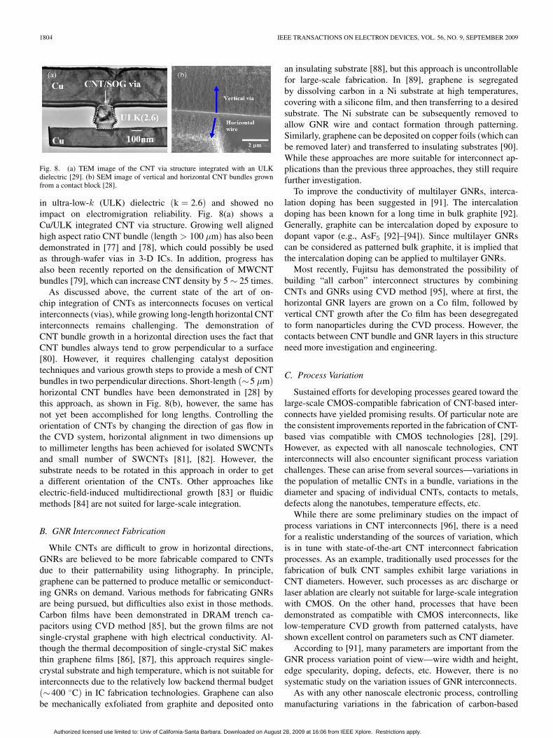
Fig. 8. (a) TEM image of the CNT via structure integrated with an ULKdielectric [29]. (b) SEM image of vertical and horizontal CNT bundles grownfrom a contact block [28].
in ultra-low-k (ULK) dielectric (k = 2.6) and showed noimpact on electromigration reliability. Fig. 8(a) shows aCu/ULK integrated CNT via structure. Growing well alignedhigh aspect ratio CNT bundle (length > 100 μm) has also beendemonstrated in [77] and [78], which could possibly be usedas through-wafer vias in 3-D ICs. In addition, progress hasalso been recently reported on the densification of MWCNTbundles [79], which can increase CNT density by 5 ∼ 25 times.
As discussed above, the current state of the art of on-chip integration of CNTs as interconnects focuses on verticalinterconnects (vias), while growing long-length horizontal CNTinterconnects remains challenging. The demonstration ofCNT bundle growth in a horizontal direction uses the fact thatCNT bundles always tend to grow perpendicular to a surface[80]. However, it requires challenging catalyst depositiontechniques and various growth steps to provide a mesh of CNTbundles in two perpendicular directions. Short-length (∼5 μm)horizontal CNT bundles have been demonstrated in [28] bythis approach, as shown in Fig. 8(b), however, the same hasnot yet been accomplished for long lengths. Controlling theorientation of CNTs by changing the direction of gas flow inthe CVD system, horizontal alignment in two dimensions upto millimeter lengths has been achieved for isolated SWCNTsand small number of SWCNTs [81], [82]. However, thesubstrate needs to be rotated in this approach in order to geta different orientation of the CNTs. Other approaches likeelectric-field-induced multidirectional growth [83] or fluidicmethods [84] are not suited for large-scale integration.
B. GNR Interconnect Fabrication
While CNTs are difficult to grow in horizontal directions,GNRs are believed to be more fabricable compared to CNTsdue to their patternability using lithography. In principle,graphene can be patterned to produce metallic or semiconduct-ing GNRs on demand. Various methods for fabricating GNRsare being pursued, but difficulties also exist in those methods.Carbon films have been demonstrated in DRAM trench ca-pacitors using CVD method [85], but the grown films are notsingle-crystal graphene with high electrical conductivity. Al-though the thermal decomposition of single-crystal SiC makesthin graphene films [86], [87], this approach requires single-crystal substrate and high temperature, which is not suitable forinterconnects due to the relatively low backend thermal budget(∼400 ◦C) in IC fabrication technologies. Graphene can alsobe mechanically exfoliated from graphite and deposited onto
an insulating substrate [88], but this approach is uncontrollablefor large-scale fabrication. In [89], graphene is segregatedby dissolving carbon in a Ni substrate at high temperatures,covering with a silicone film, and then transferring to a desiredsubstrate. The Ni substrate can be subsequently removed toallow GNR wire and contact formation through patterning.Similarly, graphene can be deposited on copper foils (which canbe removed later) and transferred to insulating substrates [90].While these approaches are more suitable for interconnect ap-plications than the previous three approaches, they still requirefurther investigation.
To improve the conductivity of multilayer GNRs, interca-lation doping has been suggested in [91]. The intercalationdoping has been known for a long time in bulk graphite [92].Generally, graphite can be intercalation doped by exposure todopant vapor (e.g., AsF5 [92]–[94]). Since multilayer GNRscan be considered as patterned bulk graphite, it is implied thatthe intercalation doping can be applied to multilayer GNRs.
Most recently, Fujitsu has demonstrated the possibility ofbuilding “all carbon” interconnect structures by combiningCNTs and GNRs using CVD method [95], where at first, thehorizontal GNR layers are grown on a Co film, followed byvertical CNT growth after the Co film has been desegregatedto form nanoparticles during the CVD process. However, thecontacts between CNT bundle and GNR layers in this structureneed more investigation and engineering.
C. Process Variation
Sustained efforts for developing processes geared toward thelarge-scale CMOS-compatible fabrication of CNT-based inter-connects have yielded promising results. Of particular note arethe consistent improvements reported in the fabrication of CNT-based vias compatible with CMOS technologies [28], [29].However, as expected with all nanoscale technologies, CNTinterconnects will also encounter significant process variationchallenges. These can arise from several sources—variations inthe population of metallic CNTs in a bundle, variations in thediameter and spacing of individual CNTs, contacts to metals,defects along the nanotubes, temperature effects, etc.
While there are some preliminary studies on the impact ofprocess variations in CNT interconnects [96], there is a needfor a realistic understanding of the sources of variation, whichis in tune with state-of-the-art CNT interconnect fabricationprocesses. As an example, traditionally used processes for thefabrication of bulk CNT samples exhibit large variations inCNT diameters. However, such processes as arc discharge orlaser ablation are clearly not suitable for large-scale integrationwith CMOS. On the other hand, processes that have beendemonstrated as compatible with CMOS interconnects, likelow-temperature CVD growth from patterned catalysts, haveshown excellent control on parameters such as CNT diameter.
According to [91], many parameters are important from theGNR process variation point of view—wire width and height,edge specularity, doping, defects, etc. However, there is nosystematic study on the variation issues of GNR interconnects.
As with any other nanoscale electronic process, controllingmanufacturing variations in the fabrication of carbon-based
Authorized licensed use limited to: Univ of California-Santa Barbara. Downloaded on August 28, 2009 at 16:06 from IEEE Xplore. Restrictions apply.

LI et al.: CARBON NANOMATERIALS FOR NEXT-GENERATION INTERCONNECTS AND PASSIVES 1805
electronics will be a significant challenge, more so because offundamental difficulties such as lack of control on chirality.Hence, modeling efforts to comprehend the relevant processvariation challenges in CNT and GNR interconnects are as im-portant as developing robust processes that minimize variations.It is instructive to note that while variation-immune/tolerantCNT/GNR interconnect design is desirable, it is important toallow the technology to reach a relatively stable and maturestage for such designs to be impactful.
IV. CNT/GNR INTERCONNECT MODELING
A. Resistance
The conductance of CNT/GNRs can be derived using thelinear response Landauer formula [97]: Gn, the conductanceof the nth conduction channel (with consideration of spin) inCNT/GNR, can be expressed as
Gn = 2e2/h ·∫
τn(E)(−∂f0/∂E) dE
f0(E) = {1 + exp [(E − EF )/kBT ]}−1 (2)
where e is the elementary charge, τn(E) is the transmissioncoefficient, f0(E) is the Fermi–Dirac distribution function,EF is the Fermi level, kB is Boltzmann’s constant, and T isthe temperature. The integration of (2) is from |En| to +∞(for electrons) or from −∞ to −|En| (for holes), where En
is the minimum (maximum) energy of the nth conduction(valence) subband, and can be obtained from the band structure,shown in Fig. 4. The factor of two in the Landauer expressionaccounts for spin degeneracy (spin up and down), and e2/his the fundamental quantum of conductance. The transmissioncoefficient τn can be influenced by defects and interaction withother electrons and phonons.
The total conductance is the sum of conductances of all theconduction and valence subbands. If all modes are assumed tobe identical, the Landauer formula (2) can be simplified as
Gtotal = 2e2/h · M · τeff (3a)
M =∑
n
[1 + exp (|En − EF |/kBT )]−1 (3b)
where Gtotal is the total conductance, M is the effective numberof allowed channels for transport, and τeff is the effectivetransmission coefficient.
Single-Walled CNTs: For SWCNTs, two bands cross at theFermi level in the band structure of the metallic (n,m) = (7, 7)CNT, as can be seen from Fig. 4, therefore M = 2. Hence,the lowest possible resistance of an isolated SWCNT, assumingperfect metal–CNT contacts (τeff = 1), is given by
RQ =h
4e2= 6.45 kΩ. (4)
This is the fundamental quantum of resistance associatedwith an SWCNT of length less than the MFP (λCNT) of elec-trons (L < λCNT). For such lengths, electron transport withinthe nanotube is essentially ballistic, and resistance is indepen-dent of length. RQ for a CNT is equally divided between thetwo metal–nanotube contacts (assuming identical contacts) on
either side. However, for lengths L > λCNT, scattering leads toan imperfect transmission coefficient [97], i.e.,
τn(E) =[
1 +L
λCNT
]−1
(5)
which yields a total resistance of
R =h
4e2
(1 +
L
λCNT
)= RQ + RS · L (6a)
RS =h
4e2· 1λCNT
(6b)
where RS is a distributed resistance per unit length, as shownin (6) (also confirmed by experimental observations [43], [98]).
In this paper, two cases of SWCNT bundle will be consid-ered: one in which all SWCNTs in the bundle are metallic(Fm = 1), and another case in which only one-third of theSWCNTs in a bundle are metallic (Fm = 1/3), the most nat-ural case [1].
MFP of CNT: It can be observed from (6) that the valueof MFP plays an important role in determining the resistanceof the nanotube. There are several scattering mechanisms forelectrons in nanotubes, including acoustic and optical phononscattering as well as impurity and defect scattering. In gen-eral, since different scattering mechanism has different scat-tering lengths and dependent parameters, the effective MFPof CNTs is a combined effect of all scattering lengths andis dependent on many parameters, such as diameter, voltagebias, length, and temperature. Interestingly, the MFP of thesedifferent scattering events are proportional to the diameterdue to the averaging out of the effective disorder over theCNT’s diameter, as has been analyzed in [99]–[101]. Thisis supported by the experimental measurement [44], whereballistic transportation was observed even for the length of25 μm in large-diameter MWCNTs. For interconnect applica-tions, it has been shown that a low-bias case is valid [102],wherein the acoustic phonon scattering will dominate. In thispaper, based on the measurement data in [43], we approximatethe electron MFP of a typical SWCNT with D = 1 nm to about1 μm. Considering its dependence of diameter, we can have
λCNT ≈ 1000 D. (7)
Note that since this MFP value is extracted from measure-ment data, it automatically takes into account the presence ofany defects in CNTs. Hence, theoretical estimation of MFP(such as in [99] and [100]) will be much larger than this value.
Multiwalled CNTs: For multiwalled CNTs (MWCNTs), dueto their large diameters, each shell could contribute to the con-ductance even if it is of semiconducting chirality [65]. In shellswith larger diameters, additional states may become populatedby thermally activated carriers, because more energy levels areaccessible. Thus, MWCNTs almost always show metallic be-havior. In this paper, we assume that the diameter of innermostshell is half of the diameter of outermost shell. Therefore, thenumber of shells (p) is given by p = 1 + [Dout/4d], whereDout is the diameter of outermost shell in a MWCNT, d is thedistance between adjacent shells (= 0.34 nm), and [·] aboveindicates that only the integral part is taken into account. For
Authorized licensed use limited to: Univ of California-Santa Barbara. Downloaded on August 28, 2009 at 16:06 from IEEE Xplore. Restrictions apply.

1806 IEEE TRANSACTIONS ON ELECTRON DEVICES, VOL. 56, NO. 9, SEPTEMBER 2009
a shell with diameter (D), the number of conducting channelsof that shell in an MWCNT can be calculated using (3b) and isapproximated as in [103]
Mshell(D) ≈ a · D + b, D > 3 nm (8)
where a = 0.0612 nm−1, and b = 0.425. Note that the as-sumption under (8) is that shells in an MWCNT have a one-third probability of having a metallic chirality and a two-thirdsprobability of having a semiconducting chirality. In addition tothe number of conducting channels, the MFP of each MWCNTshell is also different and can be calculated using (7). Using (7)and (8) in (3), the total conductance of MWCNT can be calcu-lated [65], [103]. It should be noted that the individual shellsin an MWCNT will be perturbed by adjacent shells. However,these adjacent shells are likely to have different chiralities thatproduce near random perturbations that fluctuate on a scale thatis small with respect to the nanotube diameter [55]. Hence, itcan be assumed that the electrical properties of each shell inan MWCNT will be retained, but there are resistive, capacitive,and inductive interactions among the shells, as shown in [65].
Double-Walled CNTs: Although DWCNTs are constructedfrom two SWCNTs with the same or different chiralities, theelectronic properties of each nanotube within a DWCNT canbe different from those of an isolated SWCNT. Semiconductingshells in a DWCNT may behave as metallic [104], as a resultof charge transfer and orbital mixing [105]. In this paper, weconsider the ideal case where both the inner and outer shells ofa DWCNT are metallic. For this ideal case, each DWCNT hasconducting channels M = 4.
Monolayer GNR: According to the simple tight bindingmodel (linear approximation near the Dirac point), the mini-mum (maximum) energy of the nth conduction (valence) sub-band |En| [see Fig. 4(b)] can be approximately calculated forzz-GNRs [106] as follows:
E0 = 0 (9a)|En| = (|n| + 1/2) · hvF /2w for n �= 0 (9b)
where vF = 106 m/s is the Fermi velocity, and w is the width ofthe GNR. A zero bandgap of zz-GNRs is assumed in (9a). How-ever, in reality, a bandgap is induced because of the staggeredsublattice potential from magnetic ordering once electron spinis considered when the width of zz-GNRs is small enough [19],[59]. The bandgap of zz-GNRs increases with decreasing wirewidth (the bandgap in electronvolts is 0.933/(w + 1.5) with win nm). In such situation, (9a) can be modified as
E0 =0.933
2(w + 1.5). (9c)
The transmission coefficient τn(E) in (2) is determined byboth edge scattering and scattering by defects and phonons.The edge scattering is schematically shown in Fig. 9, wherecot θ is the ratio of longitudinal (along the wire length) totransverse (across the wire width) velocities, and θ can becalculated from | sin θ| = |En/E| [107]. If complete diffusiveedge is assumed, transmission coefficient due to edge scatteringcan be expressed by “w cot θ/L,” where w cot θ is the averagedistance that electrons/holes travel before hitting the edge, and
Fig. 9. Schematic view of edge scattering in GNRs and the definition of θ. Thewidth of the GNR is w and w cot θ is the average distance that electrons/holestravel before hitting the edge. Note that L/(w cot θ) and L/(λGNR cos θ)represent the number of scattering events due to edge scattering and defectscattering, respectively. λGNR is defined along the electron/hole transportdirection (indicated by the solid arrows).
L is the length of the GNR. On the other hand, due to scatteringsby defects and phonons (not edge scattering), the transmissioncoefficient can be expressed by “λGNR cos θ/L,” where λGNR
is the MFP corresponding to such scattering. λGNR cos θ repre-sents the average distance that electrons/holes travel along theGNR longitude direction before collision. Hence, if completediffusive edge is assumed, using the Matthiessen’s rule, τn(E)can be expressed as [107]
τn(E) =(
1 +L
λGNR cos θ+
L
w cot θ
)−1
. (10)
If the edge specularity is considered, the second term in (10)needs to be modified, and the effective transmission coefficientτn(E) now should be [107]
τn(E) =[
1 + L
(1
λGNR cos θ+
1 − p
w cot θ
)]−1
(11)
where p is the edge specularity. The conductance model for ac-GNRs is complicated. Theoretical analysis indicates that ac-GNRs can be differentiated as metallic and semiconducting,but this is not valid from a practical point of view [108],since nanopatterning down to the accuracy of one atom is aformidable task. Although there are reports that graphene canbe cut along certain crystallographic directions and potentiallyproduce armchair or zigzag GNRs with smooth edges usingnanoparticles [109], this approach is not controllable: neitherthe diameter of the particles (which implies the slot width)nor the moving direction of the particles (which implies theslot direction) can be accurately controlled. Since the bandstructure of ac-GNRs changes dramatically (from semicon-ducting to metallic) with width variation, even at the atomicscale, the modeling of ac-GNR interconnect requires carefulconsideration. In this paper, we will only consider zz-GNRs forinterconnects, where small variation of width will not inducesignificant change in the band structure.
MFP of GNR: From (11), it is obvious that λGNR playsan important role in determining the conductance of GNRs.Similar to CNTs, λGNR of a monolayer GNR is proportionalto its width (w) [91], [108], theoretically, we have
λGNR ≈ 2w√3· γ2 − E2/4
σ2ε + 4σ2
γ
≈ 4w√3· γ2
2σ2ε + 8σ2
γ
(12)
where σε and σγ are the variances of different Hamiltonian ma-trix elements [99], γ = −2.7 eV, and E is the energy measured
Authorized licensed use limited to: Univ of California-Santa Barbara. Downloaded on August 28, 2009 at 16:06 from IEEE Xplore. Restrictions apply.

LI et al.: CARBON NANOMATERIALS FOR NEXT-GENERATION INTERCONNECTS AND PASSIVES 1807
with respect to EF . Comparing (7) and (12), λGNR (monolayer)can be approximately expressed as
λGNR ≈ 450w. (13)
In reality, the experimental λGNR value (∼1 μm) [45], [86], ismuch smaller than that predicted by (13), as long as the widthis not too small, which is due to the scattering from defects andis width independent. However, this is not a physical limit andcan be improved as fabrication technology progresses. In thefollowing analysis, an optimistic but arbitrary value of λGNR =5 μm is assumed for monolayer GNRs. It will be shown thateven with this optimistic MFP, monolayer GNRs cannot matchthe performance of Cu interconnects.
Multilayer GNR: To improve the total conductance, multi-layer GNRs are needed. However, when graphene layers arestacked together (typically, ABAB stacking), the MFP andconductance per layer is reduced because of intersheet electronhopping [110]. The MFP of neutral multilayer GNR (graphite)is extracted as 419 nm [107] from the in-plane conductivity of0.026 (μΩ · cm)−1 [110]. The in-plane conductivity of graphitecan be increased by several tens of magnitude by intercalationdoping, because doping can increase the carrier density due tocharge transfer and increase the MFP due to increased layerspacing (interlayer scattering is suppressed) [92]. For example,the stage 2 AsF5 intercalated graphite can have in-plane con-ductivity of 0.63 (μΩ · cm)−1, which is slightly greater than thebulk conductivity of Cu. According to [107], |EF | = 0.60 eVand the MFP for stage 2 AsF5 intercalation-doped GNR isλGNR = 1.03 μm.
It should be noted that there is report that the adjacent layersdo not interact with each other in multilayer GNRs grownon C-faced 4H-SiC (0001) [87], [111]. However, this typeof multilayer GNRs is an unlikely candidate for interconnectapplications due to two reasons: 1) Interconnect wires arefabricated on top of dielectrics, but not single-crystal SiC and2) adjacent layers are rotated by 30◦ ± 2.204◦, which impliesthat if the first GNR layer is zigzag edge, the second layerbecomes approximately armchair edge, and there is no reportof how to perform intercalation doping in such GNRs, whichwould imply low conductance.
Resistance Comparison: Fig. 10 shows the resistance com-parison for different types of CNT and GNR interconnects. Thedimension of interconnects is adapted from the InternationalTechnology Roadmap for Semicoductors (ITRS) 2008 [112]prediction for local interconnects for both 14- and 22-nm tech-nology nodes. For DWCNT, the diameter is set to be 1.5 nm.The outmost diameter of MWCNTs and the width of all GNRsare set to be equal to the wire width (W ). It can be observed thatfor all types of CNTs and GNRs, their resistances decrease withincreasing length and become stable after 10 μm (MWCNTsrequire longer length to stabilize since they have longer MFP).For wire lengths > 10 μm, all types of CNTs could offer lowerresistance than Cu, whereas only AsF5 intercalation-dopedGNRs with high edge-specularity can provide a resistancelower than that of Cu. Note that the resistance of monolayerGNR with p = 0.41 is too high and out of range in Fig. 10. Theresistance comparison shown in Fig. 10 provides insight into
Fig. 10. Resistance per unit length comparison for different types of CNTand GNR interconnects. For DWCNT, the diameter is set to be 1.5 nm, and themetallic fraction Fm = 1. The diameter of MWCNT and the width of GNR areequal to the wire width (W ). n-GNR and d-GNR represent neutral multilayerGNRs and AsF5 intercalation-doped multilayer GNRs, respectively. p is theedge specularity.
Fig. 11. Electron energy versus wave vector (k) in CNT/GNR 1-D materialwith low density of states. Equilibrium state (a) after adding charges and(b) after a current has been established. EF is the Fermi energy. The dottedline represents available states, and the solid line or shadowed area representsoccupied states. In (b), electrons move to the right in the area where ∂E/∂k >0 and to the left in the area where ∂E/∂k < 0. In order to establish a net currentfrom right to left, the number of electrons moving to the right must exceed thatmoving to the left.
the performance of CNT and GNR interconnects vis-à-vis Cuwire (discussed in more detail in Section V-A).
B. Capacitance
An external voltage applied to a 1-D conductor affects itselectrochemical potential energy in two ways. The change inelectrostatic potential energy when a charge δQ is added tothe conductor is given by (δQ)2/(2CE), where CE is itselectrostatic capacitance, which is the traditional capacitance.In addition, due to the low density of states at the Fermi energylevel, the charge δQ has to occupy available quantum energystates above the Fermi energy level as shown in Fig. 11(a).Since the density of states of CNT/GNR is low, the energyrequired to occupy higher states is high and cannot be ignored.Assuming that the additional quantum energy required to addcharge δQ to these higher energy states is eδV , followingtraditional capacitance definition, quantum capacitance can bemodeled as [113]–[116]:
CQ =δQ
δV. (14)
Hence, the net change in electrochemical potential energy isgiven by
δE =(δQ)2
2CE+
(δQ)2
2CQ=
(δQ)2
2Ctotal(15)
where Ctotal is the total effective capacitance of a 1-D con-ductor. From (15), it can be deduced that Ctotal is given by a
Authorized licensed use limited to: Univ of California-Santa Barbara. Downloaded on August 28, 2009 at 16:06 from IEEE Xplore. Restrictions apply.

1808 IEEE TRANSACTIONS ON ELECTRON DEVICES, VOL. 56, NO. 9, SEPTEMBER 2009
TABLE IIIITRS-2008-BASED SIMULATION PARAMETERS
series combination of CE and CQ. The quantum capacitanceCQ depends on the density of states at the Fermi energy levelD(μ). For each channel, it is given by [113]–[116]
CQ/channel =12e2D(μ) =
2e2
π�vF=
4e2
hvF∼ 193 aF/μm.
(16)
For metallic SWCNTs, there are two conducting channels,while for MWCNTs and GNRs, the channel number can becalculated using (3b). Note that the value of (16) is in thesame order as typical electrostatic capacitance (will be shownin Table III), therefore, for a small number of CNTs, CQ shouldnot be ignored. For conventional 3-D conductors, the density ofstates D(μ) is very large, hence, CQ is large and its effect onoverall capacitance is negligible.
Electrostatic capacitance of CNT will depend on the geom-etry of the structure. For a bundle structure, it also dependson the bundle density. As shown in [102] and [117], the mostdensely packed SWCNT bundle has slightly smaller capaci-tance compared to that of a Cu wire. As density decreases,the capacitance of CNT bundle decreases slowly. In this paper,the electrostatic capacitance of SWCNT bundle is assumedto be equal to that of Cu wire, which can be regarded asan upperbound of electrostatic capacitance for dense SWCNTbundles. Similarly, electrostatic capacitance of multilayer GNRis assumed to be equal to that of Cu wire. For MWCNTs andmonolayer GNRs, the electrostatic capacitance is calculatedby an finite-element method (FEM) tool [118]. Note that thecapacitance of the MWCNTs cannot be assumed to be equalto that of the corresponding Cu wire, due to non-negligiblefringing effects arising from the smaller number of MWCNTsin the bundle.
Fig. 12. Ratio of kinetic inductance and total effective inductance of SWCNT(with different metallic fractions Fm) and MWCNT (with different diameters)bundles as a function of interconnect width. The interconnect height is set equalto the width, and the interconnect length is 500 μm.
C. Inductance
The inductance of a conductor models the energy associatedwith the motion of electrons carrying current (I) through it. Theenergy stored in the magnetic field generated by the current isgiven by (1/2)LMI2, where LM is its magnetic inductance.For a net current δI to flow through a conductor, there has tobe an excess of electrons moving in the direction opposite tocurrent flow. Fig. 11(b) shows that there are more right movingelectrons (in the region ∂E/∂k > 0) than left moving electrons(in the region ∂E/∂k < 0) in order to establish a net current(from right to left). In a 1-D conductor that has low densityof states at the Fermi energy level (EF ), these right-movingelectrons can only be added at available quantum energy statesabove EF and, thus, have a higher kinetic energy than thoseleft-moving electrons, as shown in Fig. 11(b). This kineticenergy, stored in the moving electrons responsible for currentflow in a 1-D conductor, is modeled as
δE =12LKδI2 (17)
where LK is its kinetic inductance. The net change in energydue to current flow in the conductor is given by
δE =12LKδI2 +
12LMδI2 =
12LtotalδI
2 (18)
where Ltotal is the total effective inductance of a 1-D conductor.From (18), it can be deduced that Ltotal is given by a seriescombination of LM and LK .
For a 1-D conductor, the kinetic inductance per channel isgiven by [113]–[116], [119]
LK/channel =h
4e2vF= 8 nH/μm (19)
and it scales with the number of conducing channels. Thistheoretical value of kinetic inductance is in agreement withexperimental observations in [120].
The fraction of kinetic inductance in the total inductanceof CNT interconnects for different cross sections has beenanalyzed in [31] and shown in Fig. 12. As can be observed, ki-netic inductance forms a significant fraction of the total induc-tance when the width of SWCNT interconnects is smaller than
Authorized licensed use limited to: Univ of California-Santa Barbara. Downloaded on August 28, 2009 at 16:06 from IEEE Xplore. Restrictions apply.

LI et al.: CARBON NANOMATERIALS FOR NEXT-GENERATION INTERCONNECTS AND PASSIVES 1809
100 nm. However, it becomes much more significant in case ofMWCNT bundles. This is because the number of conductingchannels in a MWCNT bundle is small compared to that ofSWCNT bundles for a given cross section [65], and LK scalesdown linearly with number of conducting channels.
D. High-Frequency Analysis of CNT/GNR Interconnect
From traditional analysis of 3-D metal conductors, it is wellknown that the resistance and inductance of interconnects arestrongly dependent on the frequency due to skin effect and/orproximity effect. At high frequencies, the resistance of a metalwire increases significantly while inductance decreases withthe frequency. To understand the high-frequency behavior ofCNT interconnects, extracting frequency-dependent resistanceand inductance of CNT interconnect is the critical step [31]. Forthe CNT interconnect bundle structure, each CNT in the bundlewould have self-impedance and mutual impedance as follows:
Zself = RCNT + jω(Lkinetic + Lself) (20)
Zmutual = jωM (21)
where ω is the frequency, RCNT is the resistance of each CNTincluding quantum and scattering resistance (6), and Lkinetic
is the kinetic inductance of CNT. Lself and M are magneticself-inductance and mutual inductance of CNT, respectively.Note that the self-impedance of each CNT consists of resistiveand inductive (both kinetic and magnetic) impedance. However,mutual impedance (21) only consists of magnetic mutual induc-tive impedance since there is no mutual resistance and mutualkinetic inductance. The intertube resistance between CNTs ina bundle has been shown to be on the order of megaohms[98] and can be ignored. Lself and M can be obtained byemploying the concept of geometric mean distance (GMD) andarithmetic mean distance (AMD) [121]. The detailed equationsfor CNTs can be found in [31]. Therefore, for a CNT bundle,its impedance matrix is given as
[Zmatrix] =
⎡⎢⎢⎣
Z1self jωM21 · · · jωMn1
jωM21 Z2self · · · jωMn2
......
. . ....
jωMn1 jωMn2 · · · Znself
⎤⎥⎥⎦ . (22)
Having this impedance matrix, the effective total impedanceof the bundle can be obtained for a given frequency ω by solvingthe matrix equation [V ] = [Z][I], where the current vector [I]can be extracted for a given voltage V0 across the bundle. Theeffective total impedance can be obtained by
Zeff = V0/sum[I] (23)
where sum[I] is the sum of the current in each CNTs in thebundle for voltage V0. Therefore, the total effective resistanceand inductance can be obtained as
Reff = real(Zeff) (24a)
ωLeff = imag(Zeff). (24b)
Fig. 13. Total effective (a) resistance and (b) inductance of SWCNT andMWCNT bundles with different diameters as a function of frequency, comparedwith identical cross section Cu wires.
Fig. 13 shows the total effective resistance and inductancevalues of CNT interconnect as a function of frequency ascompared with a Cu wire. The resistance and inductance ofCu wire are extracted by FastHenry [122]. It can be observedthat the resistance of Cu wires increases dramatically, whilethe inductance decreases in the high-frequency region due tosignificant skin effect that reduces the effective area of cur-rent return loops. However, it is interesting to observe thatthe resistance and inductance of CNT bundle saturate at highfrequencies. Particularly for MWCNTs, their resistance almostremains unchanged, implying a negligible skin effect.
The reduced skin effect of CNT bundle can be attributed tothe presence of large kinetic inductance. Due to the existenceof kinetic inductance (= τ/σ0), the resistivity of CNT bundlebecomes complex and can be written as [119]
ρ(ω) =1 + jωτ
σ0=
1σ0
+ jωτ
σ0(25a)
τ = λ/2vF (25b)
where σ0 is the frequency-independent dc conductivity [ob-tained from (2) or (3)], τ is the momentum relaxation time, λ isthe MFP of CNTs. The second term of (25a) is the impedancedue to kinetic inductance. Based on this complex conductivity,one can derive the equivalent skin depth of a CNT bundleas [119]
δ =
√2
ωμσ0·√
[(ωτ)2 + 1] ·[√
(ωτ)2 + 1 − ωτ]
(26)
where the first term is the classical skin depth and μ is thepermeability of the material. For the case of conventionalmetals (typically τ is very small or ωτ 1), (26) reduces to theclassical skin depth. The equivalent skin depth of CNT bundleshas been calculated as shown in Fig. 14(a) [119]. It can beobserved that the skin depth of Cu wire continues to reducewith frequency, whereas the skin depths of CNTs saturate aftercertain frequencies due to existence of large kinetic inductanceor large momentum relaxation time τ . The value of this sat-uration frequency will depend on the momentum relaxationtime τ . CNTs with larger diameters have larger τ values andwill saturate earlier. It is interesting to find that MWCNTs willnot only start saturating at a relatively lower frequency butwill also have relatively large saturated skin depths. Consid-ering the fact that MWCNTs could have comparable circuit
Authorized licensed use limited to: Univ of California-Santa Barbara. Downloaded on August 28, 2009 at 16:06 from IEEE Xplore. Restrictions apply.

1810 IEEE TRANSACTIONS ON ELECTRON DEVICES, VOL. 56, NO. 9, SEPTEMBER 2009
Fig. 14. (a) Skin depth of different types of CNT materials as well as Cu asa function of frequency. (b) Ratio of high-frequency resistance with respect tothe dc resistance for different types of CNT materials and Cu [119].
performance to that of SWCNTs [65], it can be expected thatMWCNTs would have significant advantages in high-frequencyapplications.
We further evaluate the high-frequency resistance for thesemi-infinite structure shown in the inset of Fig. 14(b), wherethe width of conductor is W and the height is infinite so thatwe will only consider the skin effect along the width. Thehigh-frequency resistance of this semiinfinite structure can becalculated (detailed equations can be found in [119]) and itsratio with respect to dc resistance is shown in Fig. 14(b) forW = 1 μm. It can be observed that the resistance of Cu in-creases dramatically at high frequencies, whereas the resistanceof CNTs saturate at high frequencies. Particularly, MWCNTsexhibit only a small increase (< 9%). Also, SWCNTs withFm = 1 exhibit greater increase in resistance (w.r.t. SWCNTswith Fm = 1/3) due to larger σ0 or smaller effective kineticinductance [from (25)].
It should be noted that for traditional metals, we cannotobserve this frequency saturation effect due to the fact that thekinetic inductance is too small in conventional metals. This isdue to two reasons. First, the momentum relaxation time for ametal is usually very small (on the order of 10−14 s) [123], andthus, the imaginary part of (25a) is negligible for frequenciesless than a terahertz (ωτ 1). Moreover, the total kineticinductance also scales down with the number of conductingchannels M , which is usually very large for metals, unlessfor very small dimensions. Whereas, the momentum relaxationtime for a CNT is on the order of 10−12 s, or even larger(ωτ ∼ 1), and the M for a CNT is small (= 2 for a SWCNT).Hence, one can observe a significantly large kinetic inductancein CNTs. The above skin effect analysis of CNT materialis in agreement with our impedance extraction results shownin Fig. 13.
From the above analysis, it can be concluded that the largekinetic inductance in CNTs has two effects. The first one isthat it increases the overall inductance value. However, thisincrement becomes small (particularly for SWCNTs) for largebundle size due to the fact that total kinetic inductance scalesdown with the number of channels or number of tubes. This canbe observed in Fig. 12. The second effect is more subtle andonly becomes significant in the high-frequency region, whichleads to the reduced skin effect in CNT bundles as has beendiscussed in this section.
The unique high-frequency behavior of CNT interconnect isvery promising for high-frequency applications since one of theimportant issues in high-frequency circuit design is that the
conductor loss increases dramatically due to skin effect. Sincethe resistance of CNT interconnects increases by a smalleramount or remains almost unchanged at high frequencies, thehigh-frequency performance of the circuit can be enhancedsignificantly by employing CNT interconnects.
The high-frequency effect in multilayer GNRs is much morecomplicated than in CNTs as well as in traditional metals (Cu).Treating each GNR layer as one element is not valid in high-frequency analysis. Typically, the CNT diameter (< 40 nm)is much smaller than its classical skin depth (defined as δCSE =√
2ρeff/μω [124] where ρeff is the effective resistivity) whenfrequency is below 100 GHz. However, for the case of GNR,the width of the GNR layers (which equal the width of thewires) can be larger than the classical skin depth. Hence, thereshould be some current density redistribution within a GNRlayer. Furthermore, treating multilayer GNRs as a traditionalmetal is not valid either. The MFP of traditional metal (Cu)is 40 nm at room temperature, which is much smaller than itsclassical skin depth when frequency is below 100 GHz. TheMFP of GNR, however, is on the order of 1 μm, which can belarger than its classical skin depth. In such case, an anomalousskin effect arises [124], which requires solving the Boltzmannequation rather than using Ohm’s law for conductance calcula-tion. Quantitative analysis is required in the future to accuratelyestimate the skin effect in GNRs.
E. Thermal Modeling of CNTs
Almost all works analyzing the applicability of CNT inter-connects in VLSI circuits [64], [65], [117], have only addressedtheir electrical performance in terms of providing low-latencyhorizontal paths on a chip, except some initial analysis in [102],[125] but no thermal model was provided.
As mentioned in Section II-C, phonons dominate thermaltransport in CNTs. The thermal conductance (Gthermal
CNT ) due tophonons in a CNT can be calculated as [126]
GthermalCNT =
∑n,vn>0
∫dq
2π�ωn(q)υn(q)
∂f
∂Tτn(q, ωn) (27a)
υn(q) =∂ωn(q)
∂q(27b)
f = 1/[e�ωn/kBT − 1] (27c)
where ωn(q) is the phonon dispersion, which can be calculatedfollowing the methodology in [127], τn(q, ωn) is the energytransmission coefficient for the nth phonon branch wave atlongitudinal momentum q, f is the Bose–Einstein distributionfunction, and υn(q) is the group velocity along the direction ofthermal transport. The integration over momentum q is withinthe first Brillouin zone. The central problem in solving (27) isto find out the transmission coefficient τn(q, ωn), which willdepend on the phonon scattering.
Similar to electrical transport, for the ballistic region, wherethe CNT length is smaller than phonon MFP λph, the transmis-sion coefficient τn can be assumed to be 1. Several experimentalanalyses have demonstrated evidence of ballistic thermaltransport in CNTs. SWCNTs with diameters between 1 and
Authorized licensed use limited to: Univ of California-Santa Barbara. Downloaded on August 28, 2009 at 16:06 from IEEE Xplore. Restrictions apply.

LI et al.: CARBON NANOMATERIALS FOR NEXT-GENERATION INTERCONNECTS AND PASSIVES 1811
Fig. 15. Equivalent thermal conductivity (κCNT) for isolated thermallyballistic CNTs of different diameters as a function of (a) temperature and(b) length.
3 nm have shown ballistic thermal conductance for lengthslarger than 2 μm at room temperature [36]. MWCNTs witha diameter of 14 nm have also shown large phonon MFPs(∼500 nm) at 320 K [37]. Thermal conductance of ballisticCNTs can be calculated by (27) and the equivalent thermalconductivity (κCNT = Gthermal
CNT · L/A, where A is the areaoccupied by a CNT) is shown in Fig. 15 [128]. It is shown thatκCNT of isolated CNTs depends on their diameter, length, andtemperature. Ballistic thermal conductivity of CNTs increaseswith temperature because higher temperature will populatemore phonon modes. Moreover, the thermal conductivitydecreases with the diameter due to the fact that large diameterSWCNT occupies larger area A, but this effect is not obviousfor MWCNTs because larger diameter MWCNTs have moreshells (and thus larger thermal conductance) to counterbalancethe effect of area increase. For thermally ballistic CNTs, sincethe conductance is a constant for a given diameter CNT, largerlength also indicates higher equivalent thermal conductivity,as shown in Fig. 15(b). The large values of κCNT exceeding1000 W/m · K are shown to be achievable for isolated CNTsfor lengths exceeding 100 nm and very small diameters.
For quasi-ballistic (L ∼ λph) or diffusive region (L > λph),the thermal conductivity (κCNT) of CNT will depend on thelength, temperature, and MFP, unless L � λph where it canbe regarded as length independent. Recent molecular dynamicssimulations [129] as well as theoretical analysis [130] showthat the thermal conductivity of SWCNT follows a power law(κCNT ∝ Lα), where 0 < a < 1 dependent on length if it is inthe quasi-ballistic region. This indicates that κCNT will keepincreasing with the length even in quasi-ballistic region, andwill eventually become length independent for long lengths.Hence, if CNT based through-silicon vias (that are tens ofmicrons in height), are employed in 3-D ICs, they will havesignificant advantage due to higher thermal conductivity thanany other metals. However, the model for exponent α is stillnot determined and cannot be used in the general case. In [126],the transmission coefficient τn(q, ωn) in quasi-ballistic regionis modeled by
τn(q, ωn) =λph(ω)
λph(ω) + L. (28)
This approximation could also lead to thermal conductivity as apower law dependent on length. However, the determination ofphonon MFP is not well known. Several works in the publishedliterature express the inability to accurately predict the phononMFP in CNTs [36], [126].
For thermal modeling of CNT, understanding the phononscattering mechanism is very critical. Unfortunately, this mech-anism is not well understood yet. For quasi-ballistic re-gion, the dominant mechanism is expected to be Umklappphonon–phonon scattering. While for longer lengths, second orhigher order three-phonon scattering processes should be con-sidered [131], [132]. To fully understand the phonon scatteringmechanisms in CNTs, more experimental and theoretical workis required in the future.
V. APPLICATIONS
The physics and properties of CNTs have been studied fornearly two decades, and many possible applications for thesenanomaterials have already been widely explored. However,active research into graphene and its derivatives is a more recentdevelopment and a lot more work is needed to gauge the truepotential of GNRs. Here, we address several applications forCNTs related to interconnects and passives, alongside GNR-based interconnects that have recently been proposed.
A. CNT/GNR Interconnect
There have been several works focusing on the circuitmodeling of CNT interconnects. A simple circuit model waspresented in [113] for metallic SWCNT by using the Luttingerliquid theory [114], which explicitly separates the spin mode(does not carry charge current) and the charge mode (carriescharge current), providing insightful understanding of electrontransport in SWCNTs. By adding a distributed scattering re-sistance term to the model in [113], an RLC equivalent circuitfor SWCNTs has been proposed in [64], [102], and [117], asshown in Fig. 16(a). Subsequently, the equivalent circuit modelfor MWCNTs (also applicable to DWCNTs) has been proposedin [65] and shown in Fig. 16(b).
It should be noted that since the spin mode does not carrycharge current, an identical CNT circuit model can also bederived using different approaches by only considering thecharge mode and without involving the Luttinger liquid theory,such as those based on the semiclassical Boltzmann trans-port equation [116], the Fluid model [133],1 or an electronwaveguide transmission-line analog [134], [135]. Recently, asimilar equivalent circuit model for monolayer or multilayerGNRs has also been proposed, albeit with different conductancecalculation methods [91], [106].
The equivalent circuit model [Fig. 16(b)] for MWCNTs isdifferent from that of a SWCNT due to the fact that differentshells have different RLC parameters and there are interactionsbetween shells. Therefore, DWCNT or MWCNT is modeled astwo or more parallel RLC lines, respectively. Each RLC lineis similar to the one shown in Fig. 16(a) and represents oneshell. The details of the model for MWCNT (also valid forDWCNT) interconnect can be found in [65]. Having the equiv-alent circuits for different carbon-nanomaterial-based intercon-nects as shown in Fig. 16, their performance can be analyzedusing SPICE simulations and compared to that of a Cu wire. All
1Considers electrostatic potential as the output voltage, while other works(including this work) consider electrochemical potential as the output.
Authorized licensed use limited to: Univ of California-Santa Barbara. Downloaded on August 28, 2009 at 16:06 from IEEE Xplore. Restrictions apply.

1812 IEEE TRANSACTIONS ON ELECTRON DEVICES, VOL. 56, NO. 9, SEPTEMBER 2009
Fig. 16. Equivalent distributed circuit model of (a) an SWCNT or a GNR interconnect and (b) an MWCNT interconnect with p shells. Rmc is the imperfectcontact resistance; RQ is the quantum contact resistance; RS is the scattering-induced resistance; LK and LM are the kinetic inductance and magnetic inductanceassociated with CNTs or GNRs, respectively; M is the mutual inductance among MWCNT shells; and CQ and CE are the quantum capacitance and electrostaticcapacitance, respectively. Note that, in (b), the shell-to-shell capacitance CS and the tunneling conductance GT only have p − 1 distributed components.
Fig. 17. Signal delay ratios (with respect to Cu) of SWCNT, DWCNT,MWCNT, and different types of GNRs at the local interconnect level for the(a) 14-nm and (b) 22-nm technology nodes. Fm indicates the fraction ofmetallic SWCNTs in the SWCNT bundle, p indicates the specularity of theGNR edge. n-GNR and d-GNR represent neutral multilayer GNRs and AsF5
intercalation-doped multilayer GNRs, respectively.
simulation parameters are based on ITRS 2008 [112] predictionand have been summarized in Table III.
Fig. 17 shows the delay ratios of CNT and GNR intercon-nects with respect to Cu wire at the local level. It can beobserved that for most cases, CNT and GNR interconnects havecomparable performance to that of Cu, except for monolayerGNR. This is because the driver size at the local level istypically very small (= 2 in this work) and driver resistancedominates the total resistance of the interconnect system. SW-CNT, DWCNT and doped GNR (p = 1) are slightly better thanCu, while MWCNT is slightly worse than Cu at short lengthsbut becomes better for lengths > 0.5 μm due to the smallercapacitance of MWCNT interconnects, as shown in Table III.Monolayer GNRs are much worse than Cu at short lengthsdue to large quantum contact resistance. Note that the delayof monolayer GNR with p = 0.41 is too large to be shown inthe figure. Interestingly, for the case of p = 1, monolayer GNRstarts to outperform Cu after 2 μm because of significantlysmaller capacitance than that of Cu as shown in Table III. Itshould be noted that as the length increases further (> 5 μm),the performance of monolayer GNR becomes much worse thanthat of Cu [91] (due to the range of local interconnect’s length,this effect is not shown in Fig. 17).
Fig. 18. Signal delay ratios (with respect to Cu) of SWCNT, DWCNT, MW-CNT, and different types of GNRs at the intermediate level for the (a) 14-nmand (b) 22-nm technology nodes. Fm indicates the fraction of metallicSWCNTs in the SWCNT bundle, and p indicates the specularity of GNR edge.d-GNR represents AsF5 intercalation-doped multilayer GNRs.
Fig. 18 shows delay ratios of CNT and GNR interconnectswith respect to Cu wire at the intermediate level. It can beobserved from Fig. 18 that most CNT interconnects will out-perform Cu wire. For ideal case SWCNT and DWCNT, whereall SWCNTs and both shells in DWCNT are metallic, theyhave similar performance, both of them could obtain 30% and50% delay enhancement at length = 100 μm for 22 and 14 nm,respectively. Even for the metallic fraction Fm = 1/3 caseSWCNT, it still can provide better performance than Cu. Forthe case of MWCNTs, it is slightly worse than Cu at shortlengths due to its high resistance when length is < 10 μm, asshown in Fig. 10, but is significantly better for long lengths dueto low resistance as well as slightly smaller capacitance. Oneinteresting finding is that MWCNT could be better than idealSWCNT or DWCNT for 22 nm but worse than them for 14 nm.This is because the diameter of MWCNT is assumed to be14 nm at the 14-nm technology node and 22 nm at the 22-nmtechnology node, and because a larger diameter will havesmaller resistivity as shown in [65], MWCNT gives betterperformance at the 22-nm technology node. For GNR intercon-nects, the specularity has a very important effect on its perfor-mance. For the ideal case, where p = 1, a doped GNR couldprovide better performance than that of Cu (but is still worse
Authorized licensed use limited to: Univ of California-Santa Barbara. Downloaded on August 28, 2009 at 16:06 from IEEE Xplore. Restrictions apply.
LI et al.: CARBON NANOMATERIALS FOR NEXT-GENERATION INTERCONNECTS AND PASSIVES 1813
Fig. 19. Signal delay ratios (with respect to Cu) of SWCNT, DWCNT,MWCNT, and different types of GNRs at the global level for the (a) 14-nm and(b) 22-nm technology nodes. Fm indicates the fraction of metallic SWCNTs inthe SWCNT bundle, and p indicates the specularity of the GNR edge. d-GNRrepresents AsF5 intercalation-doped multilayer GNRs.
than the ideal SWCNT and DWCNT), however, if p = 0.41,which is a more practical case (Cu interconnects have similarspecularity value [50]), the delay of doped GNR interconnectcould be as much as 40% worse than that of Cu.
Similar results can also be observed for global-level inter-connects, as shown in Fig. 19: most CNTs outperform Cu,while a doped GNR with p = 0.41 is worse than Cu. For ideal-case SWCNTs and DWCNTs, where all SWCNTs and shells inthe DWCNT are metallic, they have similar performance, bothof them could provide more than 50% delay enhancement atlength = 1000 μm for the 22- and 14-nm technology nodes.However, at the global level, an SWCNT with Fm = 1/3 isno longer better than Cu; this is because the Cu wire width islarge at the global level, and the size effects are less evident.For global interconnects, the ideal-case GNR (doped GNRwith p = 1) still cannot be better than the ideal-case SWCNT,DWCNT, or MWCNT.
Note that we did not consider monolayer and multilayer neu-tral GNRs at the intermediate and global levels. This is becauseat the intermediate and global levels, driver sizes are usuallylarge and the interconnect lengths are long, and as a result, theresistance of the interconnect itself becomes more importantthan driver resistance. Since monolayer and multilayer neutralGNRs have much higher resistances than other materials, andsince their performance is much worse than that of Cu [91],they have been excluded in these figures.
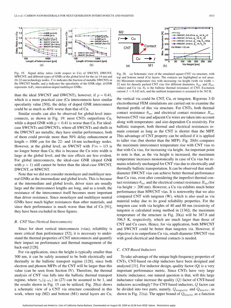
B. CNT Vias (Vertical Interconnects)
Since for short vertical interconnects (vias), reliability ismore critical than performance [52], it is necessary to under-stand the thermal properties of CNT interconnects and quantifytheir impact on performance and thermal management of theback-end [128].
For via application, since the height is typically smaller than300 nm, it can be safely assumed to be both electrically andthermally in the ballistic transport regime [128], since bothelectron and phonon MFPs of the CNT will be larger than thisvalue (can be seen from Section IV). Therefore, the thermalanalysis of CNT vias falls into the ballistic thermal transportregime, where τn(q, ωn) in (27) can be assumed to be 1, andthe results shown in Fig. 15 can be utilized. Fig. 20(a) showsa schematic view of a CNT via structure considered in thiswork, where top (M2) and bottom (M1) metal layers are Cu,
Fig. 20. (a) Schematic view of the simulated square CNT via structure, withtop and bottom metal (Cu) layers. The contacts are highlighted as red areas.(b) Maximum temperature rise with increasing via height (with via width =22 nm) for densely packed CNT vias (for different diameters, θmc and Rmc
values) and Cu via. θ0 is the ballistic thermal resistance of CNT. Excitationcurrent I = 0.142 mA, and the ambient temperature is assumed to be 363 K.
the vertical via could be CNT, Cu, or tungsten. Rigorous 3-Delectrothermal FEM simulations are carried out to examine thethermal profile of this via structure. For CNTs, both thermalcontact resistance θmc and electrical contact resistance Rmc
between CNT vias and adjacent Cu wires are taken into accountalong with temperature- and size-dependent Cu resistivity. Forballistic transport, both thermal and electrical resistances re-main constant as long as the CNT is shorter than the MFP.This advantage of CNT property can be utilized if it is appliedto taller vias (but shorter than the MFP). Fig. 20(b) comparesthe maximum interconnect temperature rise with CNT vias tothat with Cu vias, for increasing via height. An important pointto note is that, as the via height is increased, the maximumtemperature increases monotonically in case of Cu vias but re-mains relatively unchanged for CNT vias due to electrically andthermally ballistic transportation. It can be observed that small-diameter SWCNT vias can achieve better thermal performancethan Cu vias, even after considering the imperfect thermal con-tact resistance θmc and the electrical contact resistance Rmc(forvia height > 200 nm). However, a Cu via exhibits much betterperformance than MWCNT vias. It is noteworthy that we alsocompared CNT with tungsten (W), which is also used as viamaterial today due to its good reliability properties. For thetungsten case with via heights of 40 and 80 nm (resistivity oftungsten is calculated using method in [136]), the maximumtemperature of the structure in Fig. 20(a) will be 387.8 and396.5 K, respectively, which are much larger than those ofCNT and Cu cases. Hence, for via application, both MWCNTand SWCNT could be better than tungsten via. However, ifobjective is to outperform Cu via, small-diameter SWCNT viaswith good electrical and thermal contacts is needed.
C. CNT-Based Inductors
To take advantage of the unique high-frequency properties ofCNTs, CNT-based on-chip inductors have been designed andanalyzed [31]. For inductor design, quality factor (Q) is a veryimportant performance metric. Since CNTs have very largekinetic inductance, one natural question is that, will this largeinductance value increase the quality (Q) factor of CNT-basedinductors accordingly? For CNT-based inductors, Q factor canbe divided into two parts, namely, Qmagnetic and Qkinetic, asshown in Fig. 21(a). The upper bound of Qkinetic as a function
Authorized licensed use limited to: Univ of California-Santa Barbara. Downloaded on August 28, 2009 at 16:06 from IEEE Xplore. Restrictions apply.
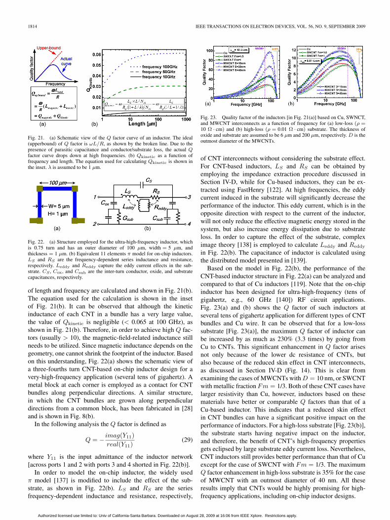
1814 IEEE TRANSACTIONS ON ELECTRON DEVICES, VOL. 56, NO. 9, SEPTEMBER 2009
Fig. 21. (a) Schematic view of the Q factor curve of an inductor. The ideal(upperbound) of Q factor is ωL/R, as shown by the broken line. Due to thepresence of parasitic capacitance and conductor/substrate loss, the actual Qfactor curve drops down at high frequencies. (b) Qkinetic as a function offrequency and length. The equation used for calculating Qkinetic is shown inthe inset. λ is assumed to be 1 μm.
Fig. 22. (a) Structure employed for the ultra-high-frequency inductor, whichis 0.75 turn and has an outer diameter of 100 μm, width = 5 μm, andthickness = 1 μm. (b) Equivalent 11 elements π model for on-chip inductors.LS and RS are the frequency-dependent series inductance and resistance,respectively. Leddy and Reddy capture the eddy current effects in the sub-strate. CS , Cox, and Csub are the inter-turn conductor, oxide, and substratecapacitances, respectively.
of length and frequency are calculated and shown in Fig. 21(b).The equation used for the calculation is shown in the insetof Fig. 21(b). It can be observed that although the kineticinductance of each CNT in a bundle has a very large value,the value of Qkinetic is negligible (< 0.065 at 100 GHz), asshown in Fig. 21(b). Therefore, in order to achieve high Q fac-tors (usually > 10), the magnetic-field-related inductance stillneeds to be utilized. Since magnetic inductance depends on thegeometry, one cannot shrink the footprint of the inductor. Basedon this understanding, Fig. 22(a) shows the schematic view ofa three-fourths turn CNT-based on-chip inductor design for avery-high-frequency application (several tens of gigahertz). Ametal block at each corner is employed as a contact for CNTbundles along perpendicular directions. A similar structure,in which the CNT bundles are grown along perpendiculardirections from a common block, has been fabricated in [28]and is shown in Fig. 8(b).
In the following analysis the Q factor is defined as
Q = − imag(Y11)real(Y11)
(29)
where Y11 is the input admittance of the inductor network[across ports 1 and 2 with ports 3 and 4 shorted in Fig. 22(b)].
In order to model the on-chip inductor, the widely usedπ model [137] is modified to include the effect of the sub-strate, as shown in Fig. 22(b). LS and RS are the seriesfrequency-dependent inductance and resistance, respectively,
Fig. 23. Quality factor of the inductors [in Fig. 21(a)] based on Cu, SWNCT,and MWCNT interconnects as a function of frequency for (a) low-loss (ρ =10 Ω · cm) and (b) high-loss (ρ = 0.01 Ω · cm) substrate. The thickness ofoxide and substrate are assumed to be 6 μm and 200 μm, respectively. D is theoutmost diameter of the MWCNTs.
of CNT interconnects without considering the substrate effect.For CNT-based inductors, LS and RS can be obtained byemploying the impedance extraction procedure discussed inSection IV-D, while for Cu-based inductors, they can be ex-tracted using FastHenry [122]. At high frequencies, the eddycurrent induced in the substrate will significantly decrease theperformance of the inductor. This eddy current, which is in theopposite direction with respect to the current of the inductor,will not only reduce the effective magnetic energy stored in thesystem, but also increase energy dissipation due to substrateloss. In order to capture the effect of the substrate, compleximage theory [138] is employed to calculate Leddy and Reddy
in Fig. 22(b). The capacitance of inductor is calculated usingthe distributed model presented in [139].
Based on the model in Fig. 22(b), the performance of theCNT-based inductor structure in Fig. 22(a) can be analyzed andcompared to that of Cu inductors [119]. Note that the on-chipinductor has been designed for ultra-high-frequency (tens ofgigahertz, e.g., 60 GHz [140]) RF circuit applications.Fig. 23(a) and (b) shows the Q factor of such inductors atseveral tens of gigahertz application for different types of CNTbundles and Cu wire. It can be observed that for a low-losssubstrate [Fig. 23(a)], the maximum Q factor of inductor canbe increased by as much as 230% (3.3 times) by going fromCu to CNTs. This significant enhancement in Q factor arisesnot only because of the lower dc resistance of CNTs, butalso because of the reduced skin effect in CNT interconnects,as discussed in Section IV-D (Fig. 14). This is clear fromexamining the cases of MWCNTs with D = 10 nm, or SWCNTwith metallic fraction Fm = 1/3. Both of these CNT cases havelarger resistivity than Cu, however, inductors based on thesematerials have better or comparable Q factors than that of aCu-based inductor. This indicates that a reduced skin effectin CNT bundles can have a significant positive impact on theperformance of inductors. For a high-loss substrate [Fig. 23(b)],the substrate starts having negative impact on the inductor,and therefore, the benefit of CNT’s high-frequency propertiesgets eclipsed by large substrate eddy current loss. Nevertheless,CNT inductors still provides better performance than that of Cuexcept for the case of SWCNT with Fm = 1/3. The maximumQ factor enhancement in high-loss substrate is 35% for the caseof MWCNT with an outmost diameter of 40 nm. All theseresults imply that CNTs would be highly promising for high-frequency applications, including on-chip inductor designs.
Authorized licensed use limited to: Univ of California-Santa Barbara. Downloaded on August 28, 2009 at 16:06 from IEEE Xplore. Restrictions apply.

LI et al.: CARBON NANOMATERIALS FOR NEXT-GENERATION INTERCONNECTS AND PASSIVES 1815
D. CNT-Based Capacitors
As a nanoscale material, one advantage of CNT is its smallform factor and high surface-area-to-volume ratio—a verydesirable property for capacitor applications [30], [141]. Capac-itors are a very important element in many IC circuits, particu-larly in RF circuits and DRAMs. From ITRS prediction, thereis no solution for MIM capacitors to fit future scaling trends,in terms of both capacitance density and leakage [112]. Theaspect ratio of present DRAM stacked capacitors is about 30 : 1and is expected to increase to more than 50 : 1 around 2012.Creating such high-aspect-ratio capacitors with straight wallsis an extremely difficult task. Aspect-ratio-dependent etchingbecomes a serious problem with each new IC generation.
One possible solution for future capacitors is to use a verticalCNT growth process, where the aspect ratio and capacitancedensity can increase dramatically. As mentioned before, alter-native bottom-up process can be implemented for CNT growth[27], which can alleviate the traditional problems associatedwith etching high aspect-ratio trenches, thereby allowing very-high-aspect-ratio capacitors, which is critical for DRAM ap-plication. In addition, due to their small form factor and highsurface-area-to-volume ratio, vertical CNT electrodes couldalso increase the capacitance density (per unit area). How-ever, CNT capacitor also has a negative aspect—a quantumcapacitance in series with electrostatic capacitance for eachCNT, which reduces the effective total capacitance. Generally,effective total capacitance can be obtained by [Ctotal]−1 =[CE ]−1 + [CQ]−1 [142], where [CE ] is the electrostatic capaci-tance matrix, off-diagonal entries in [CQ] are zero, and diagonalentries are the quantum capacitance of each CNT (CQCNT),which can be calculated as
CQCNT =
{2CQ/channel, SWCNT∑shells
Mshell(Di) · CQ/channel, MWCNT (30)
where the Mshell and CQ/channel are given in (8) and (16),respectively and Di is the diameter of the ith shell. In the simpledc cases, if CNTs are assumed to be uniform and have identicalquantum capacitance CQCNT, total capacitance calculation canbe simplified as
1Ctotal
=1
CE,tot+
1NACQCNT
+1
NCCQCNT(31)
where CE,tot is the overall effective electrostatic capacitance,which can be obtained from traditional capacitance extractiontool, such as [118], and NA and NC are the total number ofCNTs of anode and cathode, respectively.
Two feasible vertical-high-aspect-ratio CNT capacitor struc-tures are proposed in Fig. 24. All CNTs are assumed to beMWCNTs with a diameter of 20 nm, and oxide thickness is setto be 20 nm as well. Table IV summarizes the simulated capaci-tance values of these two configurations of CNT capacitors. Forthe square structure [Fig. 24(b)], we consider two cases. In onecase, CNTs are densely packed along the electrodes (distancebetween CNTs equal 0.34 nm), while in the other, CNTsare sparsely packed along the electrodes (distance betweenCNTs equal to 20 nm). Note that in the simulation, the oxide
Fig. 24. Two feasible vertical high-aspect-ratio CNT capacitor structures. Redcolor CNTs are cathode, while blue color CNTs represent anode. The CNTs areassumed to be MWCNT with a diameter of 20 nm. (a) Circular. (b) Square.
TABLE IVCNT-BASED CAPACITOR SIMULATION RESULTS
material is chosen to be silicon dioxide and the height of thecapacitor is assumed to be 1 μm, which can easily be fabricatedby a bottom-up approach [27], [30]. If larger dielectric constantoxide is chosen, or a taller vertical CNT is assumed, thecapacitance values could even be higher than those shown inTable IV.
From ITRS prediction, MIM capacitors are required toachieve a capacitance density of 7 fF/μm2 by the year 2014or 12 fF/μm2 by 2022 [112]. All the simulated CNT capacitorsshown here have much larger capacitance density than the ITRSrequirement even after considering the quantum capacitance.It can be observed from Table IV that the square capacitorstructure with densely packed CNT electrodes has the highestcapacitance density.
E. Through-Silicon Vias (TSVs)
A 3-D integration scheme reduces the number and averagelengths of the longest global wires seen in traditional planar(2-D) chips, which consequently reduces interconnect delays.In addition, this scheme leads to increased transistor pack-ing density, smaller chip area, and lower power dissipationand provides means to integrate dissimilar technologies (dig-ital, analog, RF circuits, etc) in the same chip [143], [144].High-aspect-ratio vertical interconnects, called TSVs, provid-ing connectivity between semiconductor layers, constitute a keytechnology for 3-D ICs. Unlike vias in traditional 2-D technol-ogy, TSVs can be 10–100 μm high, with an aspect ratio of 6–20.Depositing Cu or tungsten in such high aspect-ratio but narrowTSVs is very challenging.
On the other hand, it is noteworthy that “bottom-up” growthtechniques for CNT vias [27] are inherently better suited forvery high aspect-ratio vias than any “top-down” metal depo-sition technique. Well-aligned high-aspect-ratio CNT bundleshave been fabricated in [77], and furthermore, Xu et al. [78]
Authorized licensed use limited to: Univ of California-Santa Barbara. Downloaded on August 28, 2009 at 16:06 from IEEE Xplore. Restrictions apply.
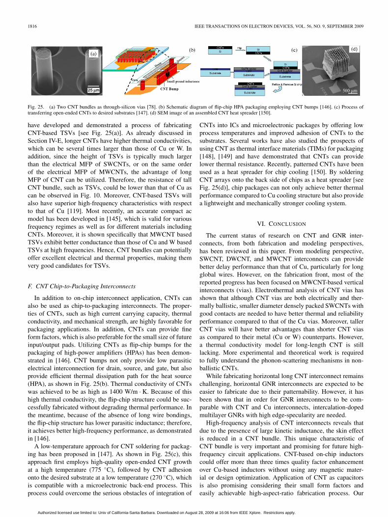
1816 IEEE TRANSACTIONS ON ELECTRON DEVICES, VOL. 56, NO. 9, SEPTEMBER 2009
Fig. 25. (a) Two CNT bundles as through-silicon vias [78]. (b) Schematic diagram of flip-chip HPA packaging employing CNT bumps [146]. (c) Process oftransferring open-ended CNTs to desired substrates [147]. (d) SEM image of an assembled CNT heat spreader [150].
have developed and demonstrated a process of fabricatingCNT-based TSVs [see Fig. 25(a)]. As already discussed inSection IV-E, longer CNTs have higher thermal conductivities,which can be several times larger than those of Cu or W. Inaddition, since the height of TSVs is typically much largerthan the electrical MFP of SWCNTs, or on the same orderof the electrical MFP of MWCNTs, the advantage of longMFP of CNT can be utilized. Therefore, the resistance of tallCNT bundle, such as TSVs, could be lower than that of Cu ascan be observed in Fig. 10. Moreover, CNT-based TSVs willalso have superior high-frequency characteristics with respectto that of Cu [119]. Most recently, an accurate compact acmodel has been developed in [145], which is valid for variousfrequency regimes as well as for different materials includingCNTs. Moreover, it is shown specifically that MWCNT basedTSVs exhibit better conductance than those of Cu and W basedTSVs at high frequencies. Hence, CNT bundles can potentiallyoffer excellent electrical and thermal properties, making themvery good candidates for TSVs.
F. CNT Chip-to-Packaging Interconnects
In addition to on-chip interconnect application, CNTs canalso be used as chip-to-packaging interconnects. The proper-ties of CNTs, such as high current carrying capacity, thermalconductivity, and mechanical strength, are highly favorable forpackaging applications. In addition, CNTs can provide fineform factors, which is also preferable for the small size of futureinput/output pads. Utilizing CNTs as flip-chip bumps for thepackaging of high-power amplifiers (HPAs) has been demon-strated in [146]. CNT bumps not only provide low parasiticelectrical interconnection for drain, source, and gate, but alsoprovide efficient thermal dissipation path for the heat source(HPA), as shown in Fig. 25(b). Thermal conductivity of CNTswas achieved to be as high as 1400 W/m · K. Because of thishigh thermal conductivity, the flip-chip structure could be suc-cessfully fabricated without degrading thermal performance. Inthe meantime, because of the absence of long wire bondings,the flip-chip structure has lower parasitic inductance; therefore,it achieves better high-frequency performance, as demonstratedin [146].
A low-temperature approach for CNT soldering for packag-ing has been proposed in [147]. As shown in Fig. 25(c), thisapproach first employs high-quality open-ended CNT growthat a high temperature (775 ◦C), followed by CNT adhesiononto the desired substrate at a low temperature (270 ◦C), whichis compatible with a microelectronic back-end process. Thisprocess could overcome the serious obstacles of integration of
CNTs into ICs and microelectronic packages by offering lowprocess temperatures and improved adhesion of CNTs to thesubstrates. Several works have also studied the prospects ofusing CNT as thermal interface materials (TIMs) for packaging[148], [149] and have demonstrated that CNTs can providelower thermal resistance. Recently, patterned CNTs have beenused as a heat spreader for chip cooling [150]. By solderingCNT arrays onto the back side of chips as a heat spreader [seeFig. 25(d)], chip packages can not only achieve better thermalperformance compared to Cu cooling structure but also providea lightweight and mechanically stronger cooling system.
VI. CONCLUSION
The current status of research on CNT and GNR inter-connects, from both fabrication and modeling perspectives,has been reviewed in this paper. From modeling perspective,SWCNT, DWCNT, and MWCNT interconnects can providebetter delay performance than that of Cu, particularly for longglobal wires. However, on the fabrication front, most of thereported progress has been focused on MWCNT-based verticalinterconnects (vias). Electrothermal analysis of CNT vias hasshown that although CNT vias are both electrically and ther-mally ballistic, smaller diameter densely packed SWCNTs withgood contacts are needed to have better thermal and reliabilityperformance compared to that of the Cu vias. Moreover, tallerCNT vias will have better advantages than shorter CNT viasas compared to their metal (Cu or W) counterparts. However,a thermal conductivity model for long-length CNT is stilllacking. More experimental and theoretical work is requiredto fully understand the phonon-scattering mechanisms in non-ballistic CNTs.
While fabricating horizontal long CNT interconnect remainschallenging, horizontal GNR interconnects are expected to beeasier to fabricate due to their patternability. However, it hasbeen shown that in order for GNR interconnects to be com-parable with CNT and Cu interconnects, intercalation-dopedmultilayer GNRs with high edge-specularity are needed.
High-frequency analysis of CNT interconnects reveals thatdue to the presence of large kinetic inductance, the skin effectis reduced in a CNT bundle. This unique characteristic ofCNT bundle is very important and promising for future high-frequency circuit applications. CNT-based on-chip inductorscould offer more than three times quality factor enhancementover Cu-based inductors without using any magnetic mater-ial or design optimization. Application of CNT as capacitorsis also promising considering their small form factors andeasily achievable high-aspect-ratio fabrication process. Our
Authorized licensed use limited to: Univ of California-Santa Barbara. Downloaded on August 28, 2009 at 16:06 from IEEE Xplore. Restrictions apply.

LI et al.: CARBON NANOMATERIALS FOR NEXT-GENERATION INTERCONNECTS AND PASSIVES 1817
simulation shows that CNT-based capacitors can achieve morethan three times higher capacitance density than that of ITRSrequirement in 2022 even with standard SiO2 dielectric andconservative CNT height of 1 μm. In addition, because of verygood electrical and thermal properties, CNTs are also verypromising for TSVs in 3-D IC integration as well as for variouschip-to-packaging interconnect applications.
APPENDIX IWHY ARE ELECTRONS AND HOLES IN
GRAPHENE MASSLESS?
The well-known relativistic energy–momentum equation canbe expressed as
Etot =√
P 2c2 + m20c
4 (A1)
where Etot is the total energy of a particle, P is the momentum,c is the speed of light, and m0 is the rest mass. The kineticenergy Ekin is the difference between total energy (Etot) of aparticle and the rest energy (m0c
2) of the particle, i.e.,
Ekin = Etot − m0c2 =
√P 2c2 + m2
0c4 − m0c
2. (A2)
When P m0c, (A2) reduces to
Ekin = P 2/2m0 (A3)
which implies the nonrelativistic case. In this case, Ekin isproportional to P 2. When m0 = 0 or the particle is massless,(A2) is reduced to
Ekin = Pc. (A4)
In such a case, Ekin is proportional to P .In graphene, since the E−k relation is linear at low energies,
we have
|E| = �vF |�k − �k0| = |�P |vF . (A5)
Therefore, the electrons and holes in graphene can be consid-ered as massless particles with a “speed of light” of vF , whichis the Fermi velocity.
It should be noted that for CNTs or GNRs, only the electrons/holes on the subband crossing the Dirac points are massless.The effective mass of electrons/holes on other subbands isnonzero and increases with higher energy subbands.
APPENDIX IIMETALLIC CONDITION OF A CNT
As stated in Section II-B, the band structure of a CNT canbe obtained as many slice cuts of (along
−→Tr shown in Fig. 26)
the energy dispersion of 2-D graphene. If the slices cut throughthe Dirac point K, there is no bandgap in the CNT’s bandstructure, and the CNT is metallic. Since the distance betweeneach slice cut is |−→Cr|, the metallic condition requires that thevertical distance between point K and
−→Tr(
−−→XK) be a multiple
of |−→Cr|. As have been proved in [1],−−→XK can be written as
−−→XK =
2n + m
3−→Cr. (A6)
Fig. 26. Brillouin zone of a CNT.−→Tr is the reciprocal vector of the translation
vector −→T , −→Cr is the reciprocal vector of the circumferential vector −→C , and K
and K′ are the Dirac points.−−→XK is the vertical distance from the Dirac point
K to −→Tr . Γ is the origin of the Brillouin zone of graphene.
Therefore, the condition for a metallic CNT requires that(2n + m), or equivalently (n − m), be a multiple of 3.
ACKNOWLEDGMENT
The authors would like to thank Dr. F. Kreupl, SanDiskCorporation, CA, Dr. A. Cassell, National Aeronautics andSpace Administration, Ames, CA, and Dr. M. Nihei, FujitsuLaboratories, Japan, for many useful discussions and feedback.
REFERENCES
[1] R. Saito, G. Dresselhaus, and S. Dresselhaus, Physical Properties ofCarbon Nanotubes. London, U. K.: Imperial College Press, 1998.
[2] S. Ijima, “Helical microtubules of graphitic carbon,” Nature, vol. 354,no. 6348, pp. 56–58, Nov. 1991.
[3] H. W. Kroto, J. R. Heath, S. C. O’Brien, R. F. Curl, and R. E. Smalley,“C60: Buckminsterfullerene,” Nature, vol. 318, no. 6042, pp. 162–163,1985.
[4] K. S. Novoselov, A. K. Geim, S. V. Morozov, D. Jiang, Y. Zhang,S. V. Dubonos, I. V. Grigorieva, and A. A. Firsov, “Electric field effect inatomically thin carbon films,” Science, vol. 306, no. 5696, pp. 666–669,Oct. 2004.
[5] P. R. Wallace, “The band theory of graphite,” Phys. Rev., vol. 71, no. 9,pp. 622–634, May 1947.
[6] P. Avouris, Z. Chen, and V. Perebeinos, “Carbon-based electronics,” Nat.Nanotechnol., vol. 2, no. 10, pp. 605–613, Oct. 2007.
[7] Q. Cao and J. A. Rogers, “Ultrathin films of single-walled carbon nano-tubes for electronics and sensors: A review of fundamental and appliedaspects,” Adv. Mater., vol. 21, no. 1, pp. 29–53, 2009.
[8] K. Tsukagoshi, B. W. Alphenaar, and H. Ago, “Coherent transport ofelectron spin in a ferromagnetically contacted carbon nanotube,” Nature,vol. 401, no. 6753, pp. 572–574, Oct. 1999.
[9] Y.-W. Son, M. L. Cohen, and S. G. Louie, “Half-metallic graphenenanoribbons,” Nature, vol. 444, no. 7117, pp. 347–350, Nov. 2006.
[10] J. A. Misewich, R. Martel, P. Avouris, J. C. Tsang, S. Heinze, andJ. Tersoff, “Electrically induced optical emission from a carbon nanotubeFET,” Science, vol. 300, no. 5620, pp. 783–786, May 2003.
[11] N. Wang, Z. K. Tang, G. D. Li, and J. S. Chen, “Materials science:Single-walled 4 Å carbon nanotube arrays,” Nature, vol. 408, no. 6808,pp. 50–51, Nov. 2000.
[12] M.-F. Yu, O. Lourie, M. J. Dyer, K. Moloni, T. F. Kelly, andR. S. Ruoff, “Strength and breaking mechanism of multiwalled carbonnanotubes under tensile load,” Science, vol. 287, no. 5453, pp. 637–640,Jan. 2000.
[13] F. Lu, L. Gu, M. J. Meziani, X. Wang, P. G. Luo, L. M. Veca, L. Cao,and Y.-P. Sun, “Advances in bioapplications of carbon nanotubes,” Adv.Mater., vol. 21, no. 2, pp. 139–152, 2009.
[14] M. I. Katsnelson and K. S. Novoselov, “Graphene: New bridge betweencondensed matter physics and quantum electrodynamics,” Solid StateCommun., vol. 143, no. 1/2, pp. 3–13, Jul. 2007.
[15] C. Du, J. Yeh, and N. Pan, “High power density supercapacitors usinglocally aligned carbon nanotube electrodes,” Nanotechnology, vol. 16,no. 4, pp. 350–353, Feb. 2005.
[16] P. Wei, W. Bao, Y. Pu, C. N. Lau, and J. Shi, “Anomalous thermoelectrictransport of Dirac particles in graphene,” Phys. Rev. Lett., vol. 102,no. 16, p. 166 808, Apr. 2009.
Authorized licensed use limited to: Univ of California-Santa Barbara. Downloaded on August 28, 2009 at 16:06 from IEEE Xplore. Restrictions apply.
1818 IEEE TRANSACTIONS ON ELECTRON DEVICES, VOL. 56, NO. 9, SEPTEMBER 2009
[17] H. Ago, K. Petritsch, M. S. P. Shaffer, A. H. Windle, and R. H. Friend,“Composites of carbon nanotubes and conjugated polymers for photo-voltaic devices,” Adv. Mater., vol. 11, no. 15, pp. 1281–1285, 1999.
[18] W. B. Choi, D. S. Chung, J. H. Kang, H. Y. Kim, Y. W. Jin, I. T. Han,Y. H. Lee, J. E. Jung, N. S. Lee, G. S. Park, and J. M. Kim, “Fullysealed, high-brightness carbon-nanotube field-emission display,” Appl.Phys. Lett., vol. 75, no. 20, pp. 3129–3131, Nov. 1999.
[19] X. Li, X. Wang, L. Zhang, S. Lee, and H. Dai, “Chemically derived,ultrasmooth graphene nanoribbon semiconductors,” Science, vol. 319,no. 5867, pp. 1229–1232, Feb. 2008.
[20] P. G. Collins, M. S. Arnold, and P. Avouris, “Engineering carbonnanotubes and nanotube circuits using electrical breakdown,” Science,vol. 292, no. 5517, pp. 706–709, Apr. 2001.
[21] H. W. C. Postma, T. Teepen, Z. Yao, M. Grifoni, and C. Dekker, “Car-bon nanotube single-electron transistors at room temperature,” Science,vol. 293, no. 5527, pp. 76–79, Jul. 2001.
[22] J. Appenzeller, Y. Lin, J. Knoch, Z. Chen, and P. Avouris, “Comparingcarbon nanotube transistors—The ideal choice: A novel tunneling devicedesign,” IEEE Trans. Electron Devices, vol. 52, no. 12, pp. 2568–2576,Dec. 2005.
[23] J. E. Jang, S. N. Cha, Y. J. Choi, D. J. Kang, T. P. Butler, D. G. Hasko,J. E. Jung, J. M. Kim, and A. J. Amaratunga, “Nanoscale memory cellbased on a nanoelectromechanical switched capacitor,” Nat. Nanotech-nol., vol. 3, no. 1, pp. 26–30, Jan. 2008.
[24] H. Dadgour, A. M. Cassell, and K. Banerjee, “Scaling and variabilityanalysis of CNT-based NEMS devices and circuits with implications forprocess design,” in IEDM Tech. Dig., 2008, pp. 529–532.
[25] Hyperion Catalysis. [Online]. Available: http://www.fibrils.com[26] F. Kreupl, A. P. Graham, G. S. Duesberg, W. Steinhogl, M. Liebau,
E. Unger, and W. Honlein, “Carbon nanotubes in interconnect ap-plications,” Microelectron. Eng., vol. 64, no. 1–4, pp. 399–408,Oct. 2002.
[27] J. Li, Q. Ye, A. Cassell, H. T. Ng, R. Stevens, J. Han, and M. Meyyappan,“Bottom-up approach for carbon nanotube interconnects,” Appl. Phys.Lett., vol. 82, no. 15, pp. 2491–2493, Apr. 2003.
[28] M. Nihei, D. Kondo, A. Kawabata, S. Sato, H. Shioya, M. Sakaue,T. Iwai, M. Ohfuti, and Y. Awano, “Low-resistance multi-walled carbonnanotube vias with parallel channel conduction of inner shells,” in Proc.IEEE Int. Interconnect Technol. Conf., 2005, pp. 234–236.
[29] A. Kawabata, S. Sato, T. Nozue, T. Hyakushima, M. Norimatsu,M. Mishima, T. Murakami, D. Kondo, K. Asano, M. Ohfuti,H. Kawarada, T. Sakai, M. Nihei, and Y. Awano, “Robustness of CNTvia interconnect fabricated by low temperature process over a high-density current,” in Proc. IEEE Int. Interconnect Technol. Conf., 2008,pp. 237–239.
[30] J. E. Jiang, S. N. Cha, Y. Choi, D.-J. Kang, D. G. Hasko, andG. A. J. Amaratunga, “Nanoscale capacitors based on metal–insulator–carbon nanotube–metal (MICNM) structures,” in Proc. ESSDERC,2005, pp. 545–547.
[31] H. Li and K. Banerjee, “High-frequency effects in carbon nanotubeinterconnects and implications for on-chip inductor design,” in IEDMTech. Dig., 2008, pp. 525–528.
[32] M. Radosavljevic, J. Lefebvre, and A. T. Johnson, “High-field electri-cal transport and breakdown in bundles of single-wall carbon nano-tubes,” Phys. Rev. B, Condens. Matter, vol. 64, no. 24, p. 241 307,Dec. 2001.
[33] B. Q. Wei, R. Vajtai, and P. M. Ajayan, “Reliability and current carryingcapacity of carbon nanotubes,” Appl. Phys. Lett., vol. 79, no. 8, pp. 1172–1174, Aug. 2001.
[34] F. Li, H. M. Cheng, S. Bai, G. Su, and M. S. Dresselhaus, “Tensilestrength of single-walled carbon nanotubes directly measured from theirmacroscopic ropes,” Appl. Phys. Lett., vol. 77, no. 20, pp. 3161–3163,Nov. 2000.
[35] J. Hone, M. Whitney, C. Piskoti, and A. Zettl, “Thermal conductivity ofsingle-walled carbon nanotubes,” Phys. Rev. B, Condens. Matter, vol. 59,no. 4, p. R2 514, 1999.
[36] C. Yu, L. Shi, Z. Yao, D. Li, and A. Majumdar, “Thermal conductanceand thermopower of an individual single-wall carbon nanotube,” NanoLett., vol. 5, no. 9, pp. 1842–1846, Jul. 2005.
[37] P. Kim, L. Shi, A. Majumdar, and P. L. McEuen, “Thermal transportmeasurements of individual multiwalled nanotubes,” Phys. Rev. Lett.,vol. 87, no. 21, p. 215 502, Oct. 2001.
[38] A. A. Balandin, S. Ghosh, W. Bao, I. Calizo, D. Teweldebrhan, F. Miao,and C. N. Lau, “Superior thermal conductivity of single-layer graphene,”Nano Lett., vol. 8, no. 3, pp. 902–907, Feb. 2008.
[39] S. Ghosh, I. Calizo, D. Teweldebrhan, E. P. Pokatilov, D. L. Nika,A. A. Balandin, W. Bao, F. Miao, and C. N. Lau, “Extremely high
thermal conductivity of graphene: Prospects for thermal managementapplications in nanoelectronic circuits,” Appl. Phys. Lett., vol. 92, no. 15,p. 151 911, Apr. 2008.
[40] C. L. Kane, E. J. Mele, R. S. Lee, J. E. Fischer, P. Petit, H. Dai,A. Thess, R. E. Smalley, A. R. M. Verschueren, S. J. Tans, and C. Dekker,“Temperature-dependent resistivity of single-wall carbon nanotubes,”Europhys. Lett., vol. 41, no. 6, pp. 683–688, Mar. 1998.
[41] T. Kwano, H. C. Chiamori, M. Suter, Q. Zhou, B. D. Sosnowchik, andL. Lin, “An electrothermal carbon nanotube gas sensor,” Nano Lett.,vol. 7, no. 12, pp. 3686–3690, Nov. 2007.
[42] Q. Shao, G. Liu, D. Teweldebrhn, and A. A. Balandin, “High-temperature quenching of electrical resistance in graphene intercon-nects,” Appl. Phys. Lett., vol. 92, no. 20, p. 202 108, May 2008.
[43] J.-Y. Park, S. Rosenblatt, Y. Yaish, V. Sazonova, H. Ustunel, S. Braig,T. A. Arias, P. W. Brouwer, and P. L. McEuen, “Electron–phonon scat-tering in metallic single-walled carbon nanotubes,” Nano Lett., vol. 4,no. 3, pp. 517–520, Feb. 2004.
[44] H. J. Li, W. G. Lu, J. J. Li, X. D. Bai, and C. Z. Gu, “Multichannel bal-listic transport in multiwall carbon nanotubes,” Phys. Rev. Lett., vol. 95,no. 8, p. 86 601, Aug. 2005.
[45] K. I. Bolotin, K. J. Sikes, J. Hone, H. L. Stormer, and P. Kim, “Tem-perature dependent transport in suspended graphene,” Phys. Rev. Lett.,vol. 101, no. 9, p. 096 802, Aug. 2008.
[46] K. M. Liew, C. H. Wong, X. Q. He, and M. J. Tan, “Thermal stabilityof single and multi-walled carbon nanotubes,” Phys. Rev. B, Condens.Matter, vol. 71, no. 7, p. 075 424, Feb. 2005.
[47] C. Lee, X. Wei, J. W. Kysar, and J. Hone, “Measurement of the elas-tic properties and intrinsic strength of monolayer graphene,” Science,vol. 321, no. 5887, pp. 385–388, Jul. 2008.
[48] Gmelin Handbook of Inorganic and Organometallic Chemistry,Springer-Verlag, Berlin, Germany, 1968.
[49] D. Gunlycke, H. M. Lawler, and C. T. White, “Room-temperature ballis-tic transport in narrow graphene strips,” Phys. Rev. B, Condens. Matter,vol. 75, no. 8, p. 085 418, Feb. 2007.
[50] W. Steinhogl, G. Schindler, G. Steinlesberger, M. Traving, andM. Engelhardt, “Comprehensive study of the resistivity of copper wireswith lateral dimensions of 100 nm and smaller,” J. Appl. Phys., vol. 97,no. 2, p. 023 706, Dec. 2005.
[51] S. Im, N. Srivastava, K. Banerjee, and K. E. Goodson, “Scalinganalysis of multilevel interconnect temperatures for high performanceICs,” IEEE Trans. Electron Devices, vol. 52, no. 12, pp. 2710–2719,Dec. 2005.
[52] N. Srivastava and K. Banerjee, “A comparative scaling analysis of metal-lic and carbon nanotube interconnections for nanometer scale VLSItechnologies,” in Proc. Int. VLSI Multilevel Interconnect Conf., 2004,pp. 393–398.
[53] N. Srivastava and K. Banerjee, “Interconnect challenges for nanoscaleelectronic circuits,” TMS J. Mater., vol. 56, no. 10, pp. 30–31, Oct. 2004.
[54] K. Banerjee and N. Srivastava, “Are carbon nanotubes the future ofVLSI interconnections?” in Proc. ACM/IEEE Des. Autom. Conf., 2006,pp. 809–814.
[55] C. T. White and J. W. Mintmire, “Fundamental properties of single-wallcarbon nanotubes,” J. Phys. Chem. B, vol. 109, no. 1, pp. 52–65, 2005.
[56] K. S. Novoselov, A. K. Geim, S. V. Morozov, D. Jiang, M. I. Katsnelson,I. V. Grigorieva, S. V. Dubonos, and A. A. Firsov, “Two-dimensional gasof massless Dirac fermions in graphene,” Nature, vol. 438, no. 7065,pp. 197–200, Nov. 2005.
[57] K. Nakada, M. Fujita, G. Dresselhaus, and M. S. Dresselhaus, “Edgestate in graphene ribbons: Nanometer size effect and edge shape de-pendence,” Phys. Rev. B, Condens. Matter, vol. 54, no. 24, pp. 17 954–17 961, Dec. 1996.
[58] L. Malysheva and A. Onipko, Dispersion of “Dispersionless Band”:Comments on L. Brey and H. A. Fertig Paper Electronic States ofGraphene Nanoribbons Studied With the Dirac Equation, May 2008.arXiv:0802.1385v2 [cond-mat.mes-hall].
[59] Y.-W. Son, M. L. Cohen, and S. G. Louie, “Energy gaps in graphenenanoribbons,” Phys. Rev. Lett., vol. 97, no. 21, p. 216 803, Nov. 2006.
[60] T. Yamamoto, S. Watanabe, and K. Watanabe, “Universal features ofquantized thermal conductance of carbon nanotubes,” Phys. Rev. Lett.,vol. 92, no. 7, p. 075 502, Feb. 2004.
[61] H.-Y. Chiu, V. V. Deshpande, H. W. Ch. Postma, N. Lau, C. Miko,L. Forro, and M. Bockrath, “Ballistic phonon thermal transport in mul-tiwalled carbon nanotubes,” Phys. Rev. Lett., vol. 95, no. 22, p. 226 101,Nov. 2005.
[62] L. G. C. Rego and G. Kirczenow, “Quantized thermal conductance ofdielectric quantum wires,” Phys. Rev. Lett., vol. 81, no. 1, pp. 232–235,1998.
Authorized licensed use limited to: Univ of California-Santa Barbara. Downloaded on August 28, 2009 at 16:06 from IEEE Xplore. Restrictions apply.

LI et al.: CARBON NANOMATERIALS FOR NEXT-GENERATION INTERCONNECTS AND PASSIVES 1819
[63] C. Kittel, Introduction to Solid State Physics, 8th ed. New York: Wiley,2004.
[64] N. Srivastava and K. Banerjee, “Performance analysis of carbon nano-tube interconnects for VLSI applications,” in Proc. IEEE/ACM Int. Conf.ICCAD, 2005, pp. 383–390.
[65] H. Li, W. Y. Yin, K. Banerjee, and J. F. Mao, “Circuit modeling andperformance analysis of multi-walled carbon nanotube interconnects,”IEEE Trans. Electron Devices, vol. 55, no. 6, pp. 1328–1337, Jun. 2008.
[66] A.-C. Dupuis, “The catalyst in the CCVD of carbon nanotubes—Areview,” Prog. Mater. Sci., vol. 50, no. 8, pp. 929–961, Nov. 2005.
[67] A. P. Graham, G. S. Duesberg, W. Hoenlein, F. Kreupl, M. Liebau,R. Martin, B. Rajasekharan, W. Pamler, R. Seidel, W. Steinhoegl,E. Unger, “How do carbon nanotubes fit into the semiconductorroadmap?” Appl. Phys. A, Solids Surf., vol. 80, no. 6, pp. 1141–1151,Mar. 2005.
[68] D. N. Futaba, K. Hata, T. Namai, T. Yamada, K. Mizuno, Y. Hayamizu,M. Yumura, and S. Iijima, “84% catalyst activity of water-assistedgrowth of single walled carbon nanotube forest characterization by astatistical and macroscopic approach,” J. Phys. Chem. B, vol. 110, no. 15,pp. 8035–8038, Mar. 2006.
[69] Y. Maeda, S. Kimura, M. Kanda, Y. Hirashima, T. Hasegawa,T. Wakahara, Y. Lian, T. Nakahodo, T. Tsuchiya, T. Akasaka, J. Lu,X. Zhang, Z. Gao, Y. Yu, S. Nagase, S. Kazaoui, N. Minami, T. Shimizu,H. Tokumoto, and R. Saito, “Large-scale separation of metallic andsemiconducting single-walled carbon nanotubes,” J. Amer. Chem. Soc.,vol. 127, no. 29, pp. 10 287–10 290, Jul. 2005.
[70] D. N. Futaba, K. Hata, T. Yamada, T. Hiraoka, Y. Hayamizu,Y. Kakudate, O. Tanaike, H. Hatori, M. Yumura, and S. Iijima, “Shape-engineerable and highly densely packed single-walled carbon nanotubesand their application as super-capacitor electrodes,” Nat. Mater., vol. 5,pp. 987–994, 2006.
[71] Y. Hayamizu, T. Yamada, K. Mizuno, R. C. Davis, D. N. Futaba,M. Yumura, and K. Hata, “Integrated three-dimensional microelectro-mechanical devices from processable carbon nanotube wafers,” Nat.Nanotechnol., vol. 3, no. 5, pp. 289–294, May 2008.
[72] Y. M. Choi, S. Lee, H. S. Yoon, M. S. Lee, H. Kim, I. Han, Y. Son,I. S. Yeo, U.-I. Chung, and J. T. Moon, “Integration and electrical prop-erties of carbon nanotube array for interconnect applications,” in Proc.IEEE Conf. Nanotechnol., 2006, pp. 262–265.
[73] M. Nihei, M. Horibe, A. Kawabata, and Y. Awano, “Simultaneous forma-tion of multiwall carbon nanotubes and their end-bonded ohmic contactsto Ti electrodes for future ULSI interconnects,” Jpn. J. Appl. Phys.,vol. 43, no. 4B, pp. 1856–1859, 2004.
[74] F. Kreupl, A. P. Graham, M. Liebau, G. S. Duesberg, R. Seidel, andE. Unger, “Carbon nanotubes for interconnect applications,” in IEDMTech. Dig., 2004, pp. 683–686.
[75] S. Sato, M. Nihei, A. Mimura, A. Kawabata, D. Kondo, H. Shioya,T. Iwai, M. Mishma, M. Ohfuti, and Y. Awano, “Novel approach to fab-ricating carbon nanotube via interconnects using size-controlled catalystnanoparticles,” in Proc. Interconnect Technol. Conf., 2006, pp. 230–232.
[76] M. Nihei, T. Hyakushima, S. Sato, T. Nozue, M. Norimatsu, M. Mishima,T. Murakami, D. Kondo, A. Kawabata, M. Ohfuti, and Y. Awano,“Electrical properties of carbon nanotube via interconnects fabricated bynovel damascene process,” in Proc. Interconnect Technol. Conf., 2007,pp. 204–206.
[77] L. Zhu, J. Xu, Y. Xiu, Y. Sun, D. W. Hess, and C. P. Wong, “Growth andelectrical characterization of high-aspect-ratio carbon nanotube arrays,”Carbon, vol. 44, no. 2, pp. 253–258, Feb. 2006.
[78] T. Xu, Z. Wang, J. Miao, X. Chen, and C. M. Tan, “Aligned carbonnanotubes for through-wafer interconnects,” Appl. Phys. Lett., vol. 91,no. 4, p. 042 108, Jul. 2007.
[79] Z. Liu, N. Bajwa, L. Ci, S. H. Lee, S. Kar, P. M. Ajayan, and J.-Q. Lu,“Densification of carbon nanotube bundles for interconnect application,”in Proc. IEEE Int. Interconnect Technol. Conf., 2007, pp. 201–203.
[80] B. Q. Wei, R. Vajtai, Y. Jung, J. Ward, Y. Zhang, G. Ramanath, andP. M. Ajayan, “Organized assembly of carbon nanotubes,” Nature,vol. 416, no. 6880, pp. 495–496, Apr. 2002.
[81] S. Huang, X. Cai, and J. Liu, “Growth of millimeter-long and horizon-tally aligned single-walled carbon nanotubes on flat substrates,” J. Amer.Chem. Soc., vol. 125, no. 19, pp. 5636–5637, Apr. 2003.
[82] H. Xin and A. T. Woolley, “Directional orientation of carbon nanotubeson surfaces using a gas flow cell,” Nano Lett., vol. 4, no. 8, pp. 1481–1484, Aug. 2004.
[83] A. Nojeh, A. Ural, R. F. Pease, and H. Dai, “Electric-field-directedgrowth of carbon nanotubes in two dimensions,” J. Vac. Sci. Technol.B, Microelectron. Process. Phenom., vol. 22, no. 6, pp. 3421–3425,Dec. 2004.
[84] Y. H. Yan, S. Li, L. Q. Chen, M. B. Chan-Park, and Q. Zhang,“Large-scale submicron horizontally aligned single-walled carbon nano-tube surface arrays on various substrates produced by a fluidic assemblymethod,” Nanotechnology, vol. 17, no. 22, pp. 5696–5701, Nov. 2006.
[85] G. Aichmayr, A. Avellán, G. S. Duesberg, F. Kreupl, S. Kudelka,M. Liebau, A. Orth, A. Sänger, J. Schumann, and O. Storbeck,“Carbon/high-k trench capacitor for the 40 nm DRAM generation,” inProc. IEEE Symp. VLSI Technol., Jun. 2007, pp. 186–187.
[86] C. Berger, Z. Song, X. Li, X. Wu, N. Brown, C. Naud, D. Mayou, T. Li,J. Hass, A. N. Marchenkov, E. H. Conrad, P. N. First, and W. A. de Heer,“Electronic confinement and coherence in patterned epitaxial graphene,”Science, vol. 312, no. 5777, pp. 1191–1196, Apr. 2006.
[87] J. Hass, R. Feng, T. Li, X. Li, Z. Zong, W. A. de Heer, P. N. First,E. H. Conrada, C. A. Jeffrey, and C. Berger, “Highly ordered graphenefor two dimensional electronics,” Appl. Phys. Lett., vol. 89, no. 14,p. 143 106, Oct. 2006.
[88] J. C. Meyer, A. K. Geim, M. I. Katsnelson, K. S. Novoselov, T. J. Booth,and S. Roth, “The structure of suspended graphene sheets,” Nature,vol. 446, no. 7131, pp. 60–63, Mar. 2007.
[89] Q. Yu, J. Lian, S. Siriponglert, H. Li, Y. P. Chen, and S.-S. Pei, “Graphenesegregated on Ni surfaces and transferred to insulators,” Appl. Phys.Lett., vol. 93, no. 11, p. 113 103, Nov. 2008.
[90] X. Li, W. Cai, J. An, S. Kim, J. Nah, D. Yang, R. Piner, A. Velamakanni,I. Jung, E. Tutuc, S. K. Banerjee, L. Colombo, and R. S. Ruoff, “Large-area synthesis of high-quality and uniform graphene films on copperfoils,” Science, vol. 324, no. 5932, p. 1312, May 2009.
[91] C. Xu, H. Li, and K. Banerjee, “Graphene nano-ribbon (GNR) intercon-nects: A genuine contender or a delusive dream?” in IEDM Tech. Dig.,2008, pp. 201–204.
[92] J. E. Fischer and T. E. Thompson, “Graphite intercalation compounds,”Phys. Today, vol. 31, no. 7, pp. 36–45, Jul. 1978.
[93] M. S. Dresselhaus and G. Dresselhaus, “Intercalation compounds ofgraphite,” Adv. Phys., vol. 51, no. 1, pp. 1–186, Jan. 2002.
[94] J. Shioya, H. Matsubara, and S. Murakami, “Properties of AsF5-intercalated vapor-grown graphite,” Synth. Met., vol. 14, no. 1/2,pp. 113–123, Mar. 1986.
[95] D. Kondo, S. Sato, and Y. Awano, “Self-organization of novel carboncomposite structure: Graphene multi-layers combined perpendicularlywith aligned carbon nanotubes,” Appl. Phys. Express, vol. 1, no. 7,p. 074 003, 2008.
[96] A. Nieuwoudt and Y. Massoud, “On the impact of process variations forcarbon nanotube bundles for VLSI interconnect,” IEEE Trans. ElectronDevices, vol. 54, no. 3, pp. 445–446, Mar. 2007.
[97] S. Datta, Electronic Transport in Mesoscopic Systems. Cambridge,U.K.: Cambridge Univ. Press, 1995.
[98] H. Stahl, J. Appenzeller, R. Martel, P. Avouris, and B. Lengeler, “Inter-tube coupling in ropes of single-wall carbon nanotubes,” Phys. Rev. Lett.,vol. 85, no. 24, pp. 5186–5189, Dec. 2000.
[99] C. T. White and T. N. Todorov, “Carbon nanotubes as long ballisticconductors,” Nature, vol. 393, pp. 240–242, 1998.
[100] J. Jiang, J. Dong, H. T. Yang, and D. Y. Xing, “Universal expression forlocalization length in metallic carbon nanotubes,” Phys. Rev. B, Condens.Matter, vol. 64, no. 4, p. 045 409, Jul. 2001.
[101] S. Roche, J. Jiang, L. F. Torres, and R. Saito, “Charge transport in carbonnanotubes: Quantum effects of electron–phonon coupling,” J. Phys.,Condens. Matter, vol. 19, no. 18, p. 183 203, Apr. 2007.
[102] N. Srivastava, H. Li, F. Kreupl, and K. Banerjee, “On the applicabilityof single-walled carbon nanotubes as VLSI interconnects,” IEEE Trans.Nanotechnol., vol. 8, no. 4, pp. 542–559, Jul. 2009.
[103] A. Naeemi and J. D. Meindl, “Compact physical models for multiwallcarbon-nanotube interconnects,” IEEE Electron Device Lett., vol. 27,no. 5, pp. 338–340, May 2006.
[104] M. Kociak, K. Suenaga, K. Hirahara, Y. Saito, T. Nakahira, andS. Iijima, “Linking chiral indices and transport properties of double-walled carbon nanotubes,” Phys. Rev. Lett., vol. 89, no. 15, p. 155 501,Oct. 2002.
[105] V. Zolyomi, J. Koltai, A. Rusznyak, J. Kurti, A. Gali, F. Simon,H. Kuzmany, A. Szabados, and P. R. Surjan, “Intershell interactionin double walled carbon nanotubes: Charge transfer and orbital mix-ing,” Phys. Rev. B, Condens. Matter, vol. 77, no. 24, p. 245 403,Jun. 2008.
[106] A. Naeemi and J. D. Meindl, “Performance benchmarking for graphenenanoribbon, carbon nanotube, and Cu interconnects,” in Proc. IEEE Int.Interconnect Technol. Conf., San Francisco, CA, 2008, pp. 183–185.
[107] C. Xu, H. Li, and K. Banerjee, “Modeling, analysis and design ofgraphene nano-ribbon interconnects,” IEEE Trans. Electron Devices,vol. 56, no. 8, pp. 1567–1578, Aug. 2009.
Authorized licensed use limited to: Univ of California-Santa Barbara. Downloaded on August 28, 2009 at 16:06 from IEEE Xplore. Restrictions apply.

1820 IEEE TRANSACTIONS ON ELECTRON DEVICES, VOL. 56, NO. 9, SEPTEMBER 2009
[108] D. A. Areshkin, D. Gunlycke, and C. T. White, “Ballistic transport ingraphene nanostrips in the presence of disorder: Importance of edgeeffects,” Nano Lett., vol. 7, no. 1, pp. 204–210, Jan. 2007.
[109] L. Ci, Z. Xu, L. Wang, W. Gao, F. Ding, K. Kelly, B. Yakobson, andP. Ajayan, “Controlled nanocutting of graphene,” Nano Res., vol. 1,no. 2, pp. 116–122, Aug. 2008.
[110] L. X. Benedict, V. H. Crespi, S. G. Louie, and M. L. Cohen, “Staticconductivity and superconductivity of carbon nanotubes: Relationsbetween tubes and sheets,” Phys. Rev. B, Condens. Matter, vol. 52,no. 20, pp. 14 935–14 940, Nov. 1995.
[111] J. Hass, F. Varchon, J. E. Millán-Otoya, M. Sprinkle, N. Sharma,W. A. de Heer, C. Berger, P. N. First, L. Magaud, and E. H. Conrad,“Why multilayer graphene on 4H-SiC (0001) behaves like a single sheetof graphene,” Phys. Rev. Lett., vol. 100, no. 12, p. 125 504, Mar. 2008.
[112] International Technology Roadmap for Semiconductors, 2008. [Online].Available: http://public.itrs.net/
[113] P. J. Burke, “Luttinger liquid theory as a model of the gigahertz electricalproperties of carbon nanotubes,” IEEE Trans. Nanotechnol., vol. 1, no. 3,pp. 129–144, Sep. 2002.
[114] M. W. Bockrath, “Carbon nanotube electrons in one dimension,” Ph.D.dissertation, Univ. California, Berkeley, CA, 1999.
[115] M. P. Anantram and F. Léonard, “Physics of carbon nanotube electronicdevices,” Rep. Prog. Phys., vol. 69, no. 3, pp. 507–561, Feb. 2006.
[116] S. Salahuddin, M. Lundstrom, and S. Datta, “Transport effects on signalpropagation in quantum wires,” IEEE Trans. Electron Devices, vol. 52,no. 8, pp. 1734–1742, Aug. 2005.
[117] A. Naeemi and J. D. Meindl, “Design and performance modeling forsingle-walled carbon nanotubes as local, semiglobal, and global inter-connects in gigascale integrated systems,” IEEE Trans. Electron De-vices, vol. 54, no. 1, pp. 26–37, Jan. 2007.
[118] S. V. Maxwell, Ansoft Corp. [Online]. Available: http://www.ansoft.com/maxwellsv/
[119] H. Li and K. Banerjee, “High-frequency analysis of carbon nanotubeinterconnects and implications for on-chip inductor design,” IEEE Trans.Electron Devices, 2009. to be published.
[120] J. J. Plombon, K. P. O’Brien, F. Gstrein, and M. Dubin, “High-frequencyelectrical properties of individual and bundled carbon nanotubes,” Appl.Phys. Lett., vol. 90, no. 6, p. 063 106, Feb. 2007.
[121] F. W. Grover, Inductance Calculations. New York: Dover, 2004.[122] M. Kamon, M. J. Tsuk, and J. White, “FastHenry: A multipole-
accelerated 3-D inductance extraction program,” IEEE Trans. Microw.Theory Tech., vol. 42, no. 9, pp. 1750–1758, Sep. 1994.
[123] N. W. Ashcroft and N. D. Mermin, Solid State Physics. Philadelphia,PA: Saunders College, 1976.
[124] E. H. Sondheimer, “The mean free path of electrons in metals,” Adv.Phys., vol. 50, no. 6, pp. 499–537, Sep. 2001.
[125] N. Srivastava, R. V. Joshi, and K. Banerjee, “Carbon nanotube inter-connect: Implications for performance, power dissipation and thermalmanagement,” in IEDM Tech. Dig., 2005, pp. 257–260.
[126] J. Wang and J.-S. Wang, “Carbon nanotube thermal transport: Ballisticto diffusive,” Appl. Phys. Lett., vol. 88, no. 11, p. 111 909, Mar. 2006.
[127] R. Saito, T. Takeya, and T. Kimura, “Raman intensity of single-wallcarbon nanotubes,” Phys. Rev. B, Condens. Matter, vol. 57, no. 7,pp. 4145–4153, Feb. 1998.
[128] H. Li, N. Srivastava, W. Y. Yin, J. F. Mao, and K. Banerjee, “Carbonnaontube vias: A reality check,” in IEDM Tech. Dig., 2007, pp. 207–210.
[129] S. Maruyama, “A molecular dynamics simulation of heat conduction ofa finite length single-walled carbon nanotube,” Microscale Thermophys.Eng., vol. 7, no. 1, pp. 41–50, 2003.
[130] N. Mingo and D. A. Broido, “Carbon nanotube ballistic thermal con-ductance and its limits,” Phys. Rev. Lett., vol. 95, no. 9, p. 096 105,Aug. 2005.
[131] N. Mingo and D.A. Broido, “Length dependence of carbon nanotubethermal conductivity and the ‘problem of long waves’,” Nano Lett.,vol. 5, no. 7, pp. 1221–1225, Jul. 2005.
[132] E. Pop, D. Mann, Q. Wang, K. Goodson, and H. Dai, “Thermal conduc-tance of an individual single-wall carbon nanotube above room temper-ature,” Nano Lett., vol. 6, no. 1, pp. 96–100, Jan. 2006.
[133] G. Miano and F. Villone, “An integral formulation for the electrodynam-ics of metallic carbon nanotubes based on a fluid model,” IEEE Trans.Antennas Propag., vol. 54, no. 10, pp. 2713–2724, Oct. 2006.
[134] J. J. Wesstrom, “Signal propagation in electron waveguides:Transmission-line analogies,” Phys. Rev. B, Condens. Matter, vol. 54,no. 16, pp. 11 484–11 491, Oct. 1996.
[135] M. S. Sarto, A. Tamburrano, and M. D’Amore, “New electron-waveguide-based modeling for carbon nanotube interconnects,” IEEETrans. Nanotechnol., vol. 8, no. 2, pp. 214–225, Mar. 2009.
[136] M. Traving, G. Schindler, and M. Engelhardt, “Damascene and subtrac-tive processing of narrow tungsten lines: Resistivity and size effect,”J. Appl. Phys., vol. 100, no. 9, p. 094 325, Nov. 2006.
[137] P. C. Yue and S. Wong, “Physical modeling of spiral inductors onsilicon,” IEEE Trans. Electron Devices, vol. 47, no. 3, pp. 560–568,Mar. 2001.
[138] A. Weisshaar and A. Luoh, “Closed-form expressions for the seriesimpedance parameters of on-chip interconnects on multilayer siliconsubstrates,” IEEE Trans. Adv. Packag., vol. 27, no. 1, pp. 126–134,Feb. 2004.
[139] C. Wu, C. Tang, and S. Liu, “Analysis of on-chip spiral inductors usingthe distributed capacitance model,” IEEE J. Solid-State Circuits, vol. 38,no. 6, pp. 1040–1044, Jun. 2003.
[140] B. Razavi, “A 60-GHz CMOS receiver front-end,” IEEE J. Solid-StateCircuits, vol. 41, no. 1, pp. 17–22, Jan. 2006.
[141] M. Budnik, A. Raychowdury, A. Bansal, and K. Roy, “A high den-sity, carbon nanotube capacitor for decoupling applications,” in Proc.ACM/IEEE Des. Autom. Conf., 2006, pp. 935–938.
[142] C. Kshirsagar, H. Li, T. Kopley, and K. Banerjee, “Accurate intrinsic gatecapacitance model for carbon nanotube-array based FETs consideringscreening effect,” IEEE Electron Device Lett., vol. 29, no. 12, pp. 1408–1411, Dec. 2008.
[143] K. Banerjee, S. J. Souri, P. Kapur, and K. C. Saraswat, “3-D ICs: A novelchip design for improving deep submicron interconnect performance andsystems-on-chip integration,” Proc. IEEE, vol. 89, no. 5, pp. 602–633,May 2001.
[144] G. L. Loi, B. Agrawal, N. Srivastava, S.-C. Lin, T. Sherwood, andK. Banerjee, “A thermally-aware performance analysis of vertically in-tegrated (3-D) processor-memory hierarchy,” in Proc. 43th ACM/IEEEDAC, 2006, pp. 991–996.
[145] C. Xu, H. Li, R. Suaya, and K. Banerjee, “Compact AC modeling andanalysis of Cu, W, and CNT based through-silicon vias (TSVs) in 3-DICs,” in IEDM Tech. Dig., 2009, to be published.
[146] T. Iwai, H. Shioya, D. Kondo, S. Hirose, A. Kawabata, S. Sato,M. Nihei, T. Kikkawa, K. Joshin, Y. Awano, and N. Yokoyama, “Thermaland source bumps utilizing carbon nanotubes for flip-chip high poweramplifiers,” in IEDM Tech. Dig., 2005, pp. 257–260.
[147] L. Zhu, Y. Sun, D. W. Hess, and C. P. Wong, “Well-aligned open-endedcarbon nanotube architectures: An approach for device assembly,” NanoLett., vol. 6, no. 2, pp. 243–247, Feb. 2006.
[148] K. Zhang and M. M. F. Yuen, “Heat spreader with aligned CNTs de-signed for thermal management of HB-LED packaging and microelec-tronic packaging,” in Proc. 7th Int. Conf. Electron. Packag. Technol.,2006, pp. 1–4.
[149] T. Tong, Y. Zhao, L. Delzeit, A. Kashani, M. Meyyappan, andA. Majumdar, “Dense vertically aligned multiwalled carbon nanotubearrays as thermal interface materials,” IEEE Trans. Compon. Packag.Technol., vol. 30, no. 1, pp. 92–100, Mar. 2007.
[150] K. Kordas, G. Toth, P. Moilanen, M. Kumpumaki, J. Vahakangas,A. Unsimaki, R. Vajtai, and P. M. Ajayan, “Chip cooling with integratedcarbon nanotube microfin architectures,” Appl. Phys. Lett., vol. 90,no. 12, p. 123 105, Mar. 2007.
Hong Li (S’07) received the B.E. degree in elec-tronic engineering from Nanjing University of Aero-nautics and Astronautics, Nanjing, China, in 2003and the M.S. degree from Shanghai Jiao Tong Uni-versity, Shanghai, China, in 2008. He has been work-ing toward the Ph.D. degree in Professor Banerjee’sNanoelectronics Research Laboratory in the De-partment of Electrical and Computer Engineering,University of California, Santa Barbara (UCSB),since 2007.
His research interests include the modeling anddesign of carbon nanomaterials for electronic applications, particularly VLSIinterconnects and passive devices. Since December 2008, he has been the LeadGraduate Student working on the development of a state-of-the-art carbonnanomaterial fabrication facility at UCSB’s California NanoSystems Institute(CNSI).
Mr. Li received numerous awards for outstanding academic performance,including the Excellent Bachelor’s Thesis Award, during his undergraduateyears.
Authorized licensed use limited to: Univ of California-Santa Barbara. Downloaded on August 28, 2009 at 16:06 from IEEE Xplore. Restrictions apply.

LI et al.: CARBON NANOMATERIALS FOR NEXT-GENERATION INTERCONNECTS AND PASSIVES 1821
Chuan Xu (S’08) received the B.S. degree in micro-electronics and the M.S. degree in microelectronicsand solid-state electronics from Peking University,Beijing, China, in 2004 and 2007, respectively. Heis currently working toward the Ph.D. degree inProf. Banerjee’s Nanoelectronics Research Labora-tory, Department of Electrical and Computer En-gineering, University of California, Santa Barbara.During his M.S. degree, he worked on the fabricationand characterization of AlGaN/GaN heterostructurefield-effect transistors.
During the summer of 2008, he was an Intern with the Electrical Interconnectand Packaging Group, IBM T. J. Watson Research Center, Yorktown Heights,NY. His current research is focused on the modeling, design, and characteriza-tion of emerging interconnect materials, structures, and effects.
Mr. Xu was the recipient of the “2008 IBM Problem Solving Award Based onthe Use of the EIP Tool Suite,” which recognizes outstanding contributions bystudents in solving the most interesting problems using IBM’s ElectromagneticField Solver Suite of Tools called the EIP tools.
Navin Srivastava (S’03) received the B.Tech.(Hons.) degree in electrical engineering from theIndian Institute of Technology, Kharagpur, India, in2000, and the M.S. and Ph.D. degrees in electri-cal and computer engineering from the Universityof California, Santa Barbara, in 2006 and 2009,respectively.
From 2000 to 2003, he was with Atrenta Inc.,India. He is currently with the Calibre Division,Mentor Graphics Corporation, Wilsonville, OR. Hisresearch interests include VLSI interconnects in
nanoelectronic circuits.Dr. Srivastava received the Outstanding Graduate Student Paper Award at
the VLSI Multilevel Interconnect Conference in 2005 and the IEEE Micro TopPicks Award in 2006.
Kaustav Banerjee (S’92–M’99–SM’03) receivedthe Ph.D. degree in electrical engineering and com-puter sciences from the University of California,Berkeley, in 1999.
In July 2002, he joined the Faculty of the De-partment of Electrical and Computer Engineering,University of California, Santa Barbara, where hehas been a Full Professor since 2007. He is alsoan affiliated faculty at the California NanoSystemsInstitute (CNSI) at UCSB. From 1999 to 2001, hewas a Research Associate with the Center for Inte-
grated Systems, Stanford University, Stanford, CA. From February to August2002, he was a Visiting Faculty with the Circuit Research Laboratories, Intel,Hillsboro, OR. He has also held summer/visiting positions at Texas InstrumentsIncorporated, Dallas, from 1993 to 1997, and the Swiss Federal Instituteof Technology, Lausanne, Switzerland, in 2001. He is the author of over170 journal and refereed international conference papers and two book chapterson 3-D ICs. He is also a coeditor of the book Emerging Nanoelectronics:Life With and After CMOS (Springer, 2004). His current research interestsinclude nanometer-scale issues in VLSI as well as circuits and systems issuesin emerging nanoelectronics. He is also involved in exploring the design andfabrication of various nanomaterials for ultra energy-efficient electronics andenergy harvesting/storage applications.
Prof. Banerjee received numerous awards in recognition of his work, in-cluding a Best Paper Award at the Design Automation Conference in 2001,the Association of Computing Machinery (ACM) Special Interest Group onDesign Automation Outstanding New Faculty Award in 2004, an IEEE MicroTop Picks Award in 2006, and an IBM Faculty Award in 2008. He hasserved on the Technical Program Committees of several leading IEEE andACM conferences, including International Electron Devices Meeting, DesignAutomation Conference, International Conference on Computer Aided Design,and International Reliability Physics Symposium. From 2005 to 2008, heserved as a member of the Nanotechnology Committee of the IEEE ElectronDevices Society. He has also served on the Organizing Committee of IEEEInternational Symposium on Quality Electronic Design at various positions,including Technical Program Chair in 2002 and General Chair in 2005. He is aDistinguished Lecturer of the IEEE Electron Devices Society.
Authorized licensed use limited to: Univ of California-Santa Barbara. Downloaded on August 28, 2009 at 16:06 from IEEE Xplore. Restrictions apply.