cb-obs411 electrical mechanical data sheet
TRANSCRIPT
connectBlue
Copyright © 2010 connectBlue AB Page 1 of 42
CB-OBS411 ELECTRICAL MECHANICAL DATASHEET
Document RevisionPublished: Jan 20, 2011 13:43 Document version: 14
Copyright © 2010 connectBlue AB. The contents of this document can be changed by connectBlue AB without prior notice and do notconstitute any binding undertakings from connectBlue AB. connectBlue AB is not responsible under any circumstances for direct, indirect,unexpected damage or consequent damage that is caused by this document. All rights reserved. All brand and product names aretrademarks or service marks of their respective owners.
connectBlue
Copyright © 2010 connectBlue AB Page 2 of 42
1 Table of Content
1 Table of Content2 Introduction
2.1 Related Documents2.2 Product Variants2.3 Block Diagram
3 Electrical Interface and Connectors3.1 Pin Numbering3.2 Pin Description3.3 Characteristics3.4 Hardware Reset
4 Operating Status5 Antennas
5.1 Surface Mounted Antennas (Internal)5.2 Antenna Connector (External antennas)
6 Mechanics6.1 Module Outlines6.2 Using the J2/J3 Board-to-Board Connectors6.3 Using Press-Fit Nuts for Mounting the Module6.4 Using the J6 PCB solder pads6.5 Antenna Issues
7 Bluetooth Information7.1 General information7.2 Bluetooth Qualification information
8 Regulatory Information8.1 Declaration of Conformity8.2 Safety Compliance8.3 FCC and IC Compliance8.4 UL listing information8.5 Compliance with RoHS directive
9 Guidelines for Efficient and Safe Use9.1 General9.2 Product Care9.3 Radio Frequency Exposure9.4 Electronic Equipment9.5 Potentially Explosive Atmospheres9.6 Power Supply
10 Application Notes10.1 Step-by-Step Guide10.2 Design Examples
connectBlue
Copyright © 2010 connectBlue AB Page 3 of 42
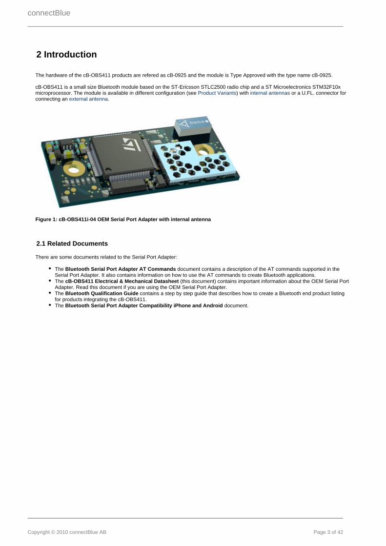
2 Introduction
The hardware of the cB-OBS411 products are refered as cB-0925 and the module is Type Approved with the type name cB-0925.
cB-OBS411 is a small size Bluetooth module based on the ST-Ericsson STLC2500 radio chip and a ST Microelectronics STM32F10xmicroprocessor. The module is available in different configuration (see ) with or a U.FL. connector forProduct Variants internal antennasconnecting an . external antenna
Figure 1: cB-OBS411i-04 OEM Serial Port Adapter with internal antenna
2.1 Related Documents
There are some documents related to the Serial Port Adapter:
The document contains a description of the AT commands supported in theBluetooth Serial Port Adapter AT CommandsSerial Port Adapter. It also contains information on how to use the AT commands to create Bluetooth applications.The (this document) contains important information about the OEM Serial PortcB-OBS411 Electrical & Mechanical DatasheetAdapter. Read this document if you are using the OEM Serial Port Adapter.The contains a step by step guide that describes how to create a Bluetooth end product listingBluetooth Qualification Guidefor products integrating the cB-OBS411.The document.Bluetooth Serial Port Adapter Compatibility iPhone and Android
connectBlue
Copyright © 2010 connectBlue AB Page 4 of 42
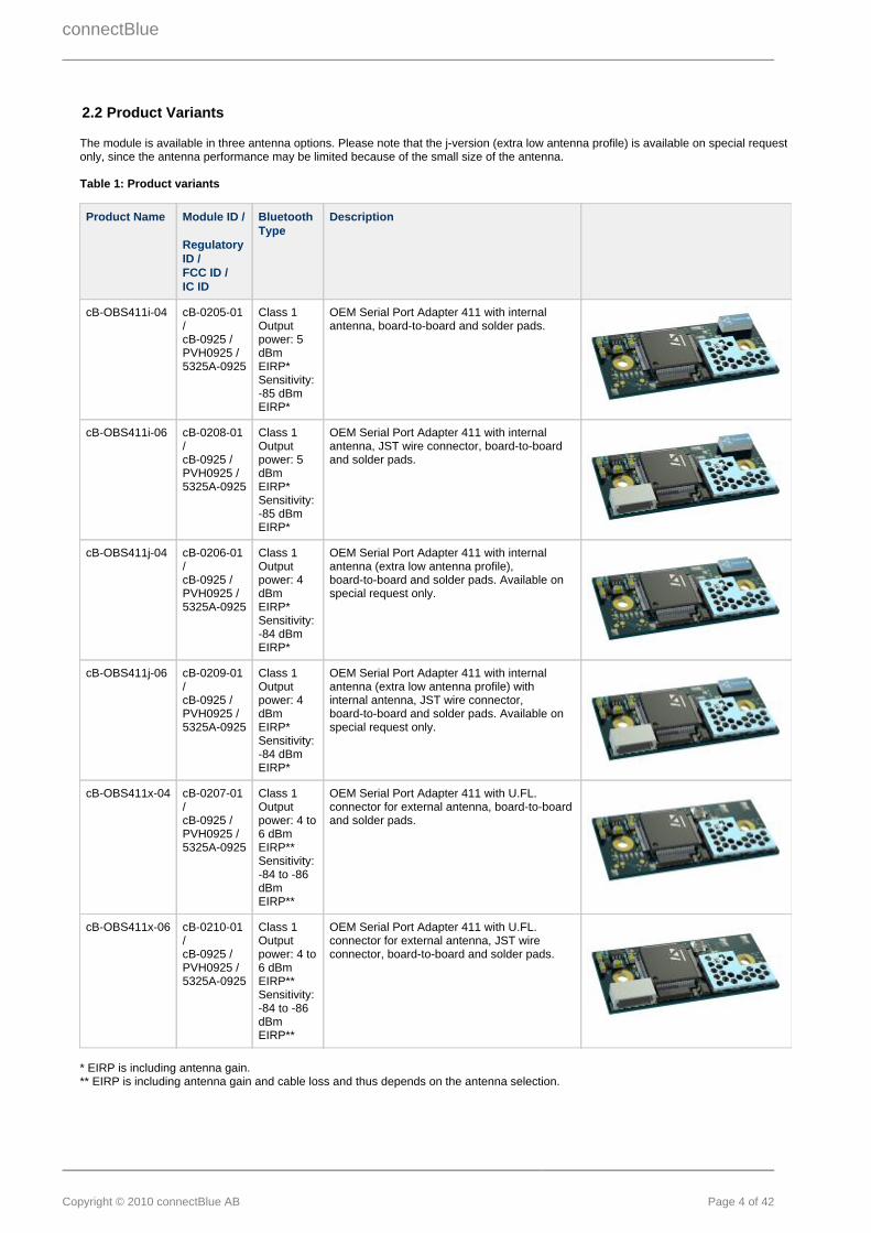
2.2 Product Variants
The module is available in three antenna options. Please note that the j-version (extra low antenna profile) is available on special requestonly, since the antenna performance may be limited because of the small size of the antenna.
Table 1: Product variants
Product Name Module ID /
RegulatoryID / FCC ID / IC ID
BluetoothType
Description
cB-OBS411i-04 cB-0205-01/ cB-0925 / PVH0925 / 5325A-0925
Class 1 Outputpower: 5dBmEIRP* Sensitivity:-85 dBmEIRP*
OEM Serial Port Adapter 411 with internalantenna, board-to-board and solder pads.
cB-OBS411i-06 cB-0208-01/ cB-0925 / PVH0925 / 5325A-0925
Class 1 Outputpower: 5dBmEIRP* Sensitivity:-85 dBmEIRP*
OEM Serial Port Adapter 411 with internalantenna, JST wire connector, board-to-boardand solder pads.
cB-OBS411j-04 cB-0206-01/ cB-0925 / PVH0925 / 5325A-0925
Class 1 Outputpower: 4dBmEIRP* Sensitivity:-84 dBmEIRP*
OEM Serial Port Adapter 411 with internalantenna (extra low antenna profile),board-to-board and solder pads. Available onspecial request only.
cB-OBS411j-06 cB-0209-01/ cB-0925 / PVH0925 / 5325A-0925
Class 1 Outputpower: 4dBmEIRP* Sensitivity:-84 dBmEIRP*
OEM Serial Port Adapter 411 with internalantenna (extra low antenna profile) withinternal antenna, JST wire connector,board-to-board and solder pads. Available onspecial request only.
cB-OBS411x-04 cB-0207-01/ cB-0925 / PVH0925 / 5325A-0925
Class 1 Outputpower: 4 to6 dBmEIRP** Sensitivity:-84 to -86dBmEIRP**
OEM Serial Port Adapter 411 with U.FL.connector for external antenna, board-to-boardand solder pads.
cB-OBS411x-06 cB-0210-01/ cB-0925 / PVH0925 / 5325A-0925
Class 1 Outputpower: 4 to6 dBmEIRP** Sensitivity:-84 to -86dBmEIRP**
OEM Serial Port Adapter 411 with U.FL.connector for external antenna, JST wireconnector, board-to-board and solder pads.
* EIRP is including antenna gain.** EIRP is including antenna gain and cable loss and thus depends on the antenna selection.

connectBlue
Copyright © 2010 connectBlue AB Page 5 of 42
2.3 Block Diagram
Figure 2: Block diagram of cB-OBS411
connectBlue
Copyright © 2010 connectBlue AB Page 6 of 42
3 Electrical Interface and Connectors
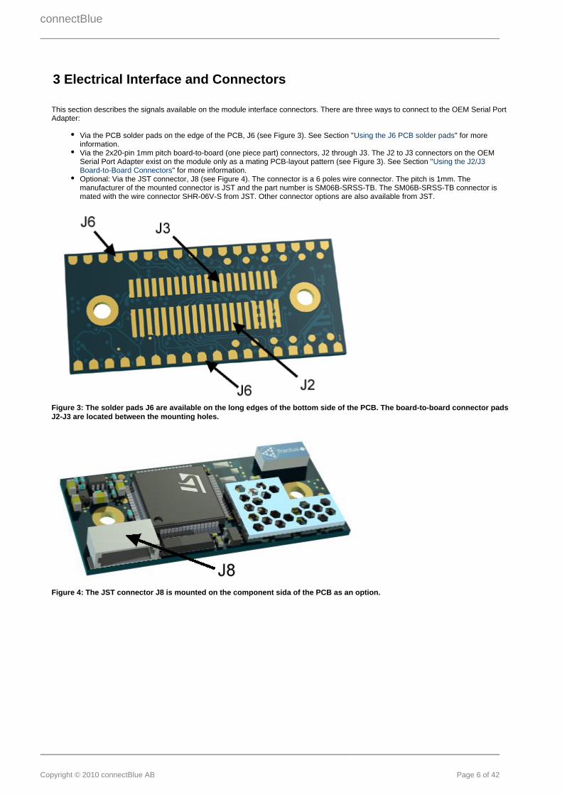
This section describes the signals available on the module interface connectors. There are three ways to connect to the OEM Serial PortAdapter:
Via the PCB solder pads on the edge of the PCB, J6 (see Figure 3). See Section " " for moreUsing the J6 PCB solder padsinformation.Via the 2x20-pin 1mm pitch board-to-board (one piece part) connectors, J2 through J3. The J2 to J3 connectors on the OEMSerial Port Adapter exist on the module only as a mating PCB-layout pattern (see Figure 3). See Section "Using the J2/J3
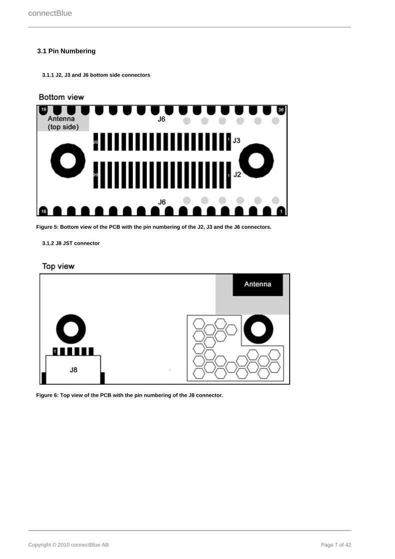
" for more information.Board-to-Board ConnectorsOptional: Via the JST connector, J8 (see Figure 4). The connector is a 6 poles wire connector. The pitch is 1mm. Themanufacturer of the mounted connector is JST and the part number is SM06B-SRSS-TB. The SM06B-SRSS-TB connector ismated with the wire connector SHR-06V-S from JST. Other connector options are also available from JST.
Figure 3: The solder pads J6 are available on the long edges of the bottom side of the PCB. The board-to-board connector padsJ2-J3 are located between the mounting holes.
Figure 4: The JST connector J8 is mounted on the component sida of the PCB as an option.
connectBlue
Copyright © 2010 connectBlue AB Page 7 of 42
3.1 Pin Numbering
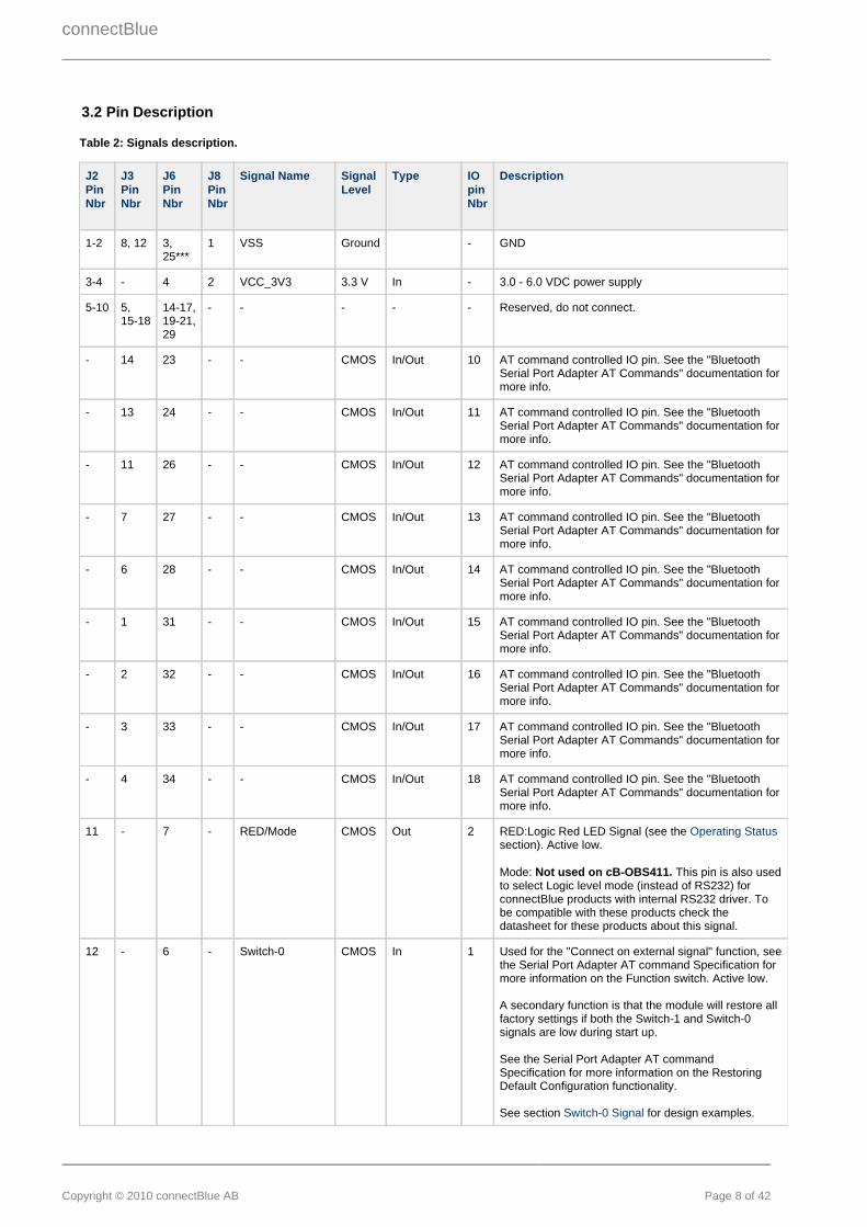
3.1.1 J2, J3 and J6 bottom side connectors
Figure 5: Bottom view of the PCB with the pin numbering of the J2, J3 and the J6 connectors.
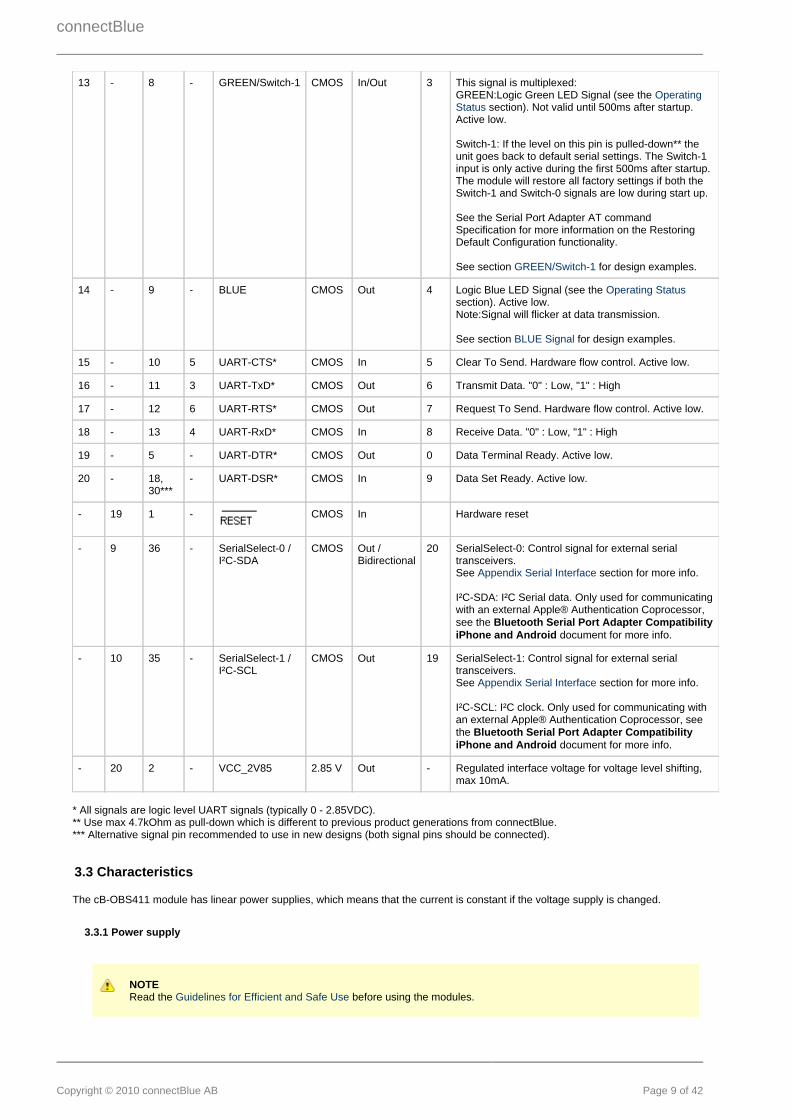
3.1.2 J8 JST connector
Figure 6: Top view of the PCB with the pin numbering of the J8 connector.
connectBlue
Copyright © 2010 connectBlue AB Page 8 of 42
3.2 Pin Description
Table 2: Signals description.
J2PinNbr
J3 PinNbr
J6PinNbr
J8PinNbr
Signal Name SignalLevel
Type IOpinNbr
Description
1-2 8, 12 3,25***
1 VSS Ground - GND
3-4 - 4 2 VCC_3V3 3.3 V In - 3.0 - 6.0 VDC power supply
5-10 5,15-18
14-17,19-21,29
- - - - - Reserved, do not connect.
- 14 23 - - CMOS In/Out 10 AT command controlled IO pin. See the "BluetoothSerial Port Adapter AT Commands" documentation formore info.
- 13 24 - - CMOS In/Out 11 AT command controlled IO pin. See the "BluetoothSerial Port Adapter AT Commands" documentation formore info.
- 11 26 - - CMOS In/Out 12 AT command controlled IO pin. See the "BluetoothSerial Port Adapter AT Commands" documentation formore info.
- 7 27 - - CMOS In/Out 13 AT command controlled IO pin. See the "BluetoothSerial Port Adapter AT Commands" documentation formore info.
- 6 28 - - CMOS In/Out 14 AT command controlled IO pin. See the "BluetoothSerial Port Adapter AT Commands" documentation formore info.
- 1 31 - - CMOS In/Out 15 AT command controlled IO pin. See the "BluetoothSerial Port Adapter AT Commands" documentation formore info.
- 2 32 - - CMOS In/Out 16 AT command controlled IO pin. See the "BluetoothSerial Port Adapter AT Commands" documentation formore info.
- 3 33 - - CMOS In/Out 17 AT command controlled IO pin. See the "BluetoothSerial Port Adapter AT Commands" documentation formore info.
- 4 34 - - CMOS In/Out 18 AT command controlled IO pin. See the "BluetoothSerial Port Adapter AT Commands" documentation formore info.
11 - 7 - RED/Mode CMOS Out 2 RED:Logic Red LED Signal (see the Operating Statussection). Active low.
Mode: This pin is also usedNot used on cB-OBS411.to select Logic level mode (instead of RS232) forconnectBlue products with internal RS232 driver. Tobe compatible with these products check thedatasheet for these products about this signal.
12 - 6 - Switch-0 CMOS In 1 Used for the "Connect on external signal" function, seethe Serial Port Adapter AT command Specification formore information on the Function switch. Active low.
A secondary function is that the module will restore allfactory settings if both the Switch-1 and Switch-0signals are low during start up.
See the Serial Port Adapter AT commandSpecification for more information on the RestoringDefault Configuration functionality.
See section for design examples.Switch-0 Signal
connectBlue
Copyright © 2010 connectBlue AB Page 9 of 42
13 - 8 - GREEN/Switch-1 CMOS In/Out 3 This signal is multiplexed: GREEN:Logic Green LED Signal (see the Operating
section). Not valid until 500ms after startup.StatusActive low.
Switch-1: If the level on this pin is pulled-down** theunit goes back to default serial settings. The Switch-1input is only active during the first 500ms after startup.The module will restore all factory settings if both theSwitch-1 and Switch-0 signals are low during start up. See the Serial Port Adapter AT commandSpecification for more information on the RestoringDefault Configuration functionality.
See section for design examples.GREEN/Switch-1
14 - 9 - BLUE CMOS Out 4 Logic Blue LED Signal (see the Operating Statussection). Active low. Note:Signal will flicker at data transmission.
See section for design examples.BLUE Signal
15 - 10 5 UART-CTS* CMOS In 5 Clear To Send. Hardware flow control. Active low.
16 - 11 3 UART-TxD* CMOS Out 6 Transmit Data. "0" : Low, "1" : High
17 - 12 6 UART-RTS* CMOS Out 7 Request To Send. Hardware flow control. Active low.
18 - 13 4 UART-RxD* CMOS In 8 Receive Data. "0" : Low, "1" : High
19 - 5 - UART-DTR* CMOS Out 0 Data Terminal Ready. Active low.
20 - 18,30***
- UART-DSR* CMOS In 9 Data Set Ready. Active low.
- 19 1 - CMOS In Hardware reset
- 9 36 - SerialSelect-0 /I²C-SDA
CMOS Out /Bidirectional
20 SerialSelect-0: Control signal for external serialtransceivers. See section for more info. Appendix Serial Interface
I²C-SDA: I²C Serial data. Only used for communicatingwith an external Apple® Authentication Coprocessor,see the Bluetooth Serial Port Adapter Compatibility
document for more info.iPhone and Android
- 10 35 - SerialSelect-1 /I²C-SCL
CMOS Out 19 SerialSelect-1: Control signal for external serialtransceivers. See section for more info. Appendix Serial Interface
I²C-SCL: I²C clock. Only used for communicating withan external Apple® Authentication Coprocessor, seethe Bluetooth Serial Port Adapter Compatibility
document for more info. iPhone and Android
- 20 2 - VCC_2V85 2.85 V Out - Regulated interface voltage for voltage level shifting,max 10mA.
* All signals are logic level UART signals (typically 0 - 2.85VDC).** Use max 4.7kOhm as pull-down which is different to previous product generations from connectBlue.*** Alternative signal pin recommended to use in new designs (both signal pins should be connected).
3.3 Characteristics
The cB-OBS411 module has linear power supplies, which means that the current is constant if the voltage supply is changed.
3.3.1 Power supply
NOTERead the before using the modules.Guidelines for Efficient and Safe Use
connectBlue
Copyright © 2010 connectBlue AB Page 10 of 42
Table 3: Power supply
Symbol Parameter Value Unit
VCC_3V3 Power supply (Unregulated*) Min 3.0 VDC
Max 6.0 VDC
The module is equipped with internal linear voltage regulators.
Table 4: Current consumption
Symbol Mode Value Unit
I @ VCC_3V3 = 3.3VCC Not connected Connectable, discoverable Average 14.5 mA
Peak 64.5 mA
Not connected, stop mode enabled Not connectable, not discoverable Average 0.6 mA
Peak 0.6 mA
Connectable, not discoverable Average 0.8 mA
Peak 37.2 mA
Connectable, discoverable Average 1.2 mA
Peak 37.2 mA
Connected Idle or Receiving Average 15.5 mA
Peak 57.8 mA
Transmitting @115.2kbit/s Average 25.1 mA
Peak 64.9 mA
Inquiry Average 35.5 mA
Peak 71.0 mA
3.3.2 Input/Output signals
Table 5: Input/output signals
Symbol Parameter Value Unit
V LowIN Logic LOW level input voltage Min -0.50 V
Max 0.80 V
V HighIN UART Logic HIGH level input voltage UART interface and RED signal Min 2.00 V
Max 5.50 V
V HighIN Logic HIGH level input voltage all other IO pins Min 2.00 V
Max 3.35 V
V LowOUT Logic LOW level output voltage Max 0.40 V
V HighOUT Logic HIGH level output voltage Min 2.40 V
IIO Sink and source current Max 8 mA
CIO I/O pin capacitance Typ 5 pF
connectBlue
Copyright © 2010 connectBlue AB Page 11 of 42
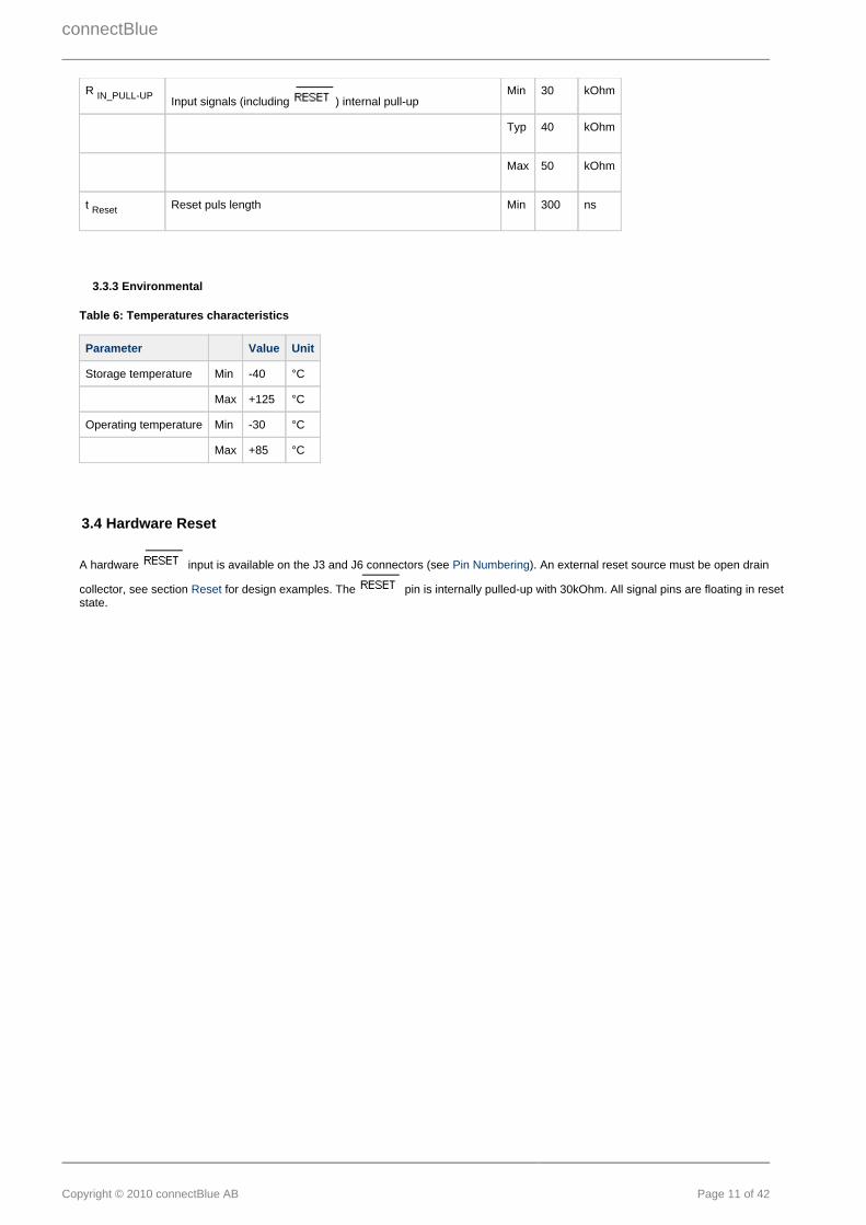
R IN_PULL-UP Input signals (including ) internal pull-up Min 30 kOhm
Typ 40 kOhm
Max 50 kOhm
t Reset Reset puls length Min 300 ns
3.3.3 Environmental
Table 6: Temperatures characteristics
Parameter Value Unit
Storage temperature Min -40 °C
Max +125 °C
Operating temperature Min -30 °C
Max +85 °C
3.4 Hardware Reset
A hardware input is available on the J3 and J6 connectors (see ). An external reset source must be open drainPin Numbering
collector, see section for design examples. The pin is internally pulled-up with 30kOhm. All signal pins are floating in resetResetstate.
connectBlue
Copyright © 2010 connectBlue AB Page 12 of 42
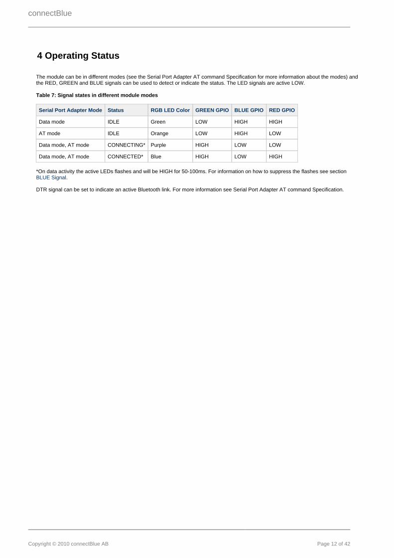
4 Operating Status
The module can be in different modes (see the Serial Port Adapter AT command Specification for more information about the modes) andthe RED, GREEN and BLUE signals can be used to detect or indicate the status. The LED signals are active LOW.
Table 7: Signal states in different module modes
Serial Port Adapter Mode Status RGB LED Color GREEN GPIO BLUE GPIO RED GPIO
Data mode IDLE Green LOW HIGH HIGH
AT mode IDLE Orange LOW HIGH LOW
Data mode, AT mode CONNECTING* Purple HIGH LOW LOW
Data mode, AT mode CONNECTED* Blue HIGH LOW HIGH
*On data activity the active LEDs flashes and will be HIGH for 50-100ms. For information on how to suppress the flashes see section .BLUE Signal
DTR signal can be set to indicate an active Bluetooth link. For more information see Serial Port Adapter AT command Specification.
connectBlue
Copyright © 2010 connectBlue AB Page 13 of 42
5 Antennas
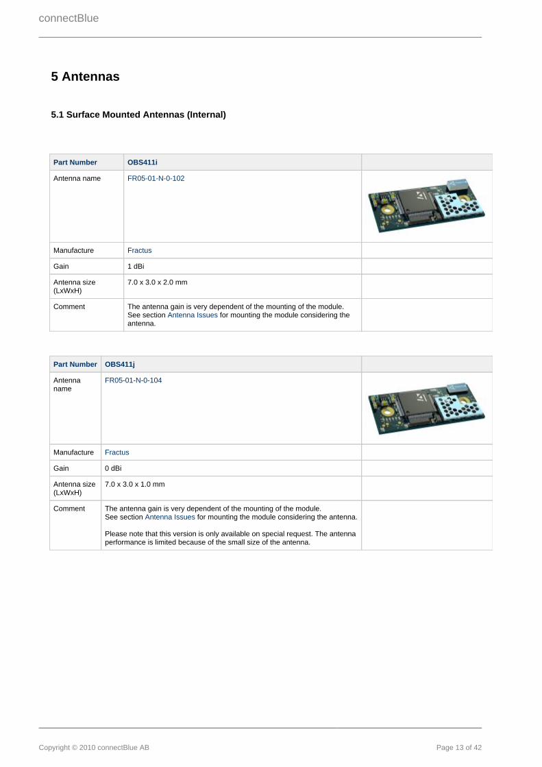
5.1 Surface Mounted Antennas (Internal)
Part Number OBS411i
Antenna name FR05-01-N-0-102
Manufacture Fractus
Gain 1 dBi
Antenna size(LxWxH)
7.0 x 3.0 x 2.0 mm
Comment The antenna gain is very dependent of the mounting of the module. See section for mounting the module considering theAntenna Issuesantenna.
Part Number OBS411j
Antennaname
FR05-01-N-0-104
Manufacture Fractus
Gain 0 dBi
Antenna size(LxWxH)
7.0 x 3.0 x 1.0 mm
Comment The antenna gain is very dependent of the mounting of the module. See section for mounting the module considering the antenna.Antenna Issues
Please note that this version is only available on special request. The antennaperformance is limited because of the small size of the antenna.
connectBlue
Copyright © 2010 connectBlue AB Page 14 of 42
5.2 Antenna Connector (External antennas)
The external antennas are connected to the board through a U.FL connector. Some of the antennas are connected directly to the U.FLconnector of the board and some are connected using an SMA or reversed polarity SMA connector through a short U.FL to SMA orreversed polarity SMA adapter cable. The SMA antenna versions are not allowed for usage in USA and Canada. Instead the reversedpolarity SMA must be used. Other antennas are also available on request (please contact connectBlue for more information).
5.2.1 Antenna Accessories
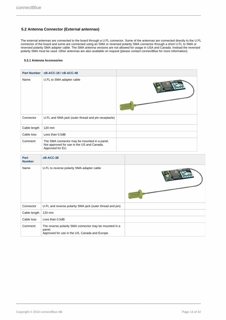
Part Number cB-ACC-18 / cB-ACC-48
Name U.FL to SMA adapter cable
Connector U.FL and SMA jack (outer thread and pin receptacle)
Cable length 120 mm
Cable loss Less than 0.5dB
Comment The SMA connector may be mounted in a panel. Not approved for use in the US and Canada. Approved for EU.
PartNumber
cB-ACC-38
Name U.FL to reverse polarity SMA adapter cable
Connector U.FL and reverse polarity SMA jack (outer thread and pin)
Cable length 120 mm
Cable loss Less than 0.5dB
Comment The reverse polarity SMA connector may be mounted in apanel. Approved for use in the US, Canada and Europe.
connectBlue
Copyright © 2010 connectBlue AB Page 15 of 42
5.2.2 Antennas
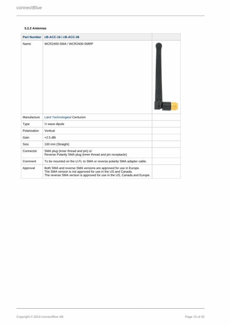
Part Number cB-ACC-16 / cB-ACC-36
Name WCR2400-SMA / WCR2400-SMRP
Manufacture / Centurion Laird Technologies
Type ½ wave dipole
Polarization Vertical
Gain +2.5 dBi
Size 100 mm (Straight)
Connector SMA plug (inner thread and pin) or Reverse Polarity SMA plug (inner thread and pin receptacle)
Comment To be mounted on the U.FL to SMA or reverse polarity SMA adapter cable.
Approval Both SMA and reverse SMA versions are approved for use in Europe. The SMA version is not approved for use in the US and Canada. The reverse SMA version is approved for use in the US, Canada and Europe.
connectBlue
Copyright © 2010 connectBlue AB Page 16 of 42
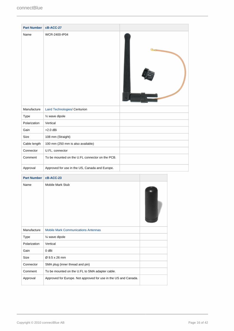
Part Number cB-ACC-27
Name WCR-2400-IP04
Manufacture / Centurion Laird Technologies
Type ½ wave dipole
Polarization Vertical
Gain +2.0 dBi
Size 108 mm (Straight)
Cable length 100 mm (250 mm is also available)
Connector U.FL. connector
Comment To be mounted on the U.FL connector on the PCB.
Approval Approved for use in the US, Canada and Europe.
Part Number cB-ACC-23
Name Mobile Mark Stub
Manufacture Mobile Mark Communications Antennas
Type ¼ wave dipole
Polarization Vertical
Gain 0 dBi
Size Ø 9.5 x 26 mm
Connector SMA plug (inner thread and pin)
Comment To be mounted on the U.FL to SMA adapter cable.
Approval Approved for Europe. Not approved for use in the US and Canada.

connectBlue
Copyright © 2010 connectBlue AB Page 17 of 42
PartNumber
cB-ACC-17
Name Reel planTec Bluetooth m70
Manufacture REEL
Type Patch antenna
Gain +1.0 dBi
Size Ø 75 x 20 mm
Mounting M16 x 13.6 mm
Connector SMA plug (inner thread and pin)
Cablelength
300 cm. Other cable lengths are availableon request.
Comment To be mounted on the U.FL to SMAadapter cable.
Approval Approved for Europe. Not approved for usein the US and Canada. Please contact connectBlue for informationabout US and Canada approved versionsof the antenna with reverse polarity SMAplug connector.
connectBlue
Copyright © 2010 connectBlue AB Page 18 of 42
PartNumber
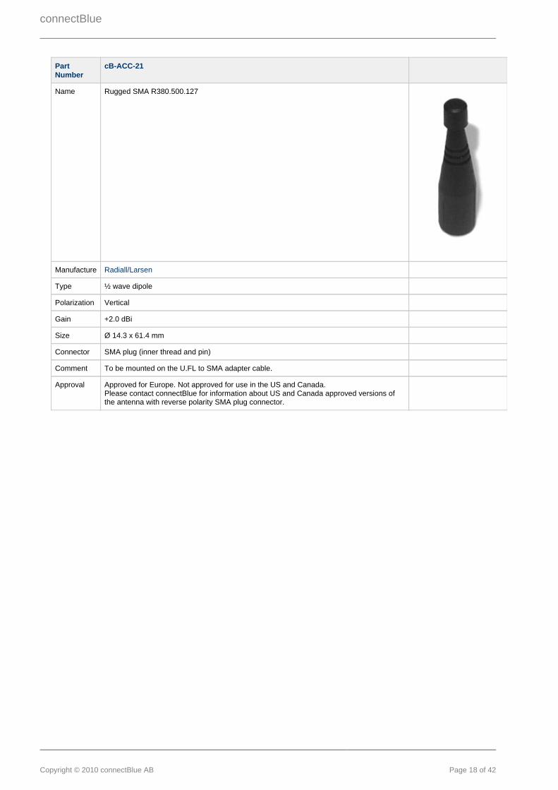
cB-ACC-21
Name Rugged SMA R380.500.127
Manufacture Radiall/Larsen
Type ½ wave dipole
Polarization Vertical
Gain +2.0 dBi
Size Ø 14.3 x 61.4 mm
Connector SMA plug (inner thread and pin)
Comment To be mounted on the U.FL to SMA adapter cable.
Approval Approved for Europe. Not approved for use in the US and Canada. Please contact connectBlue for information about US and Canada approved versions ofthe antenna with reverse polarity SMA plug connector.
connectBlue
Copyright © 2010 connectBlue AB Page 19 of 42
6 Mechanics
6.1 Module Outlines
6.1.1 Dimensions
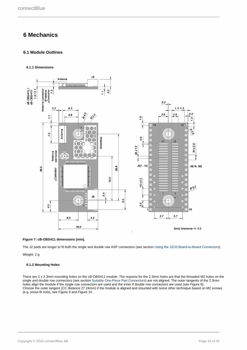
Figure 7: cB-OBS411 dimensions [mm].
The J2 pads are longer to fit both the single and double row ASP connectors (see section ).Using the J2/J3 Board-to-Board Connectors
Weight: 2 g
6.1.2 Mounting Holes
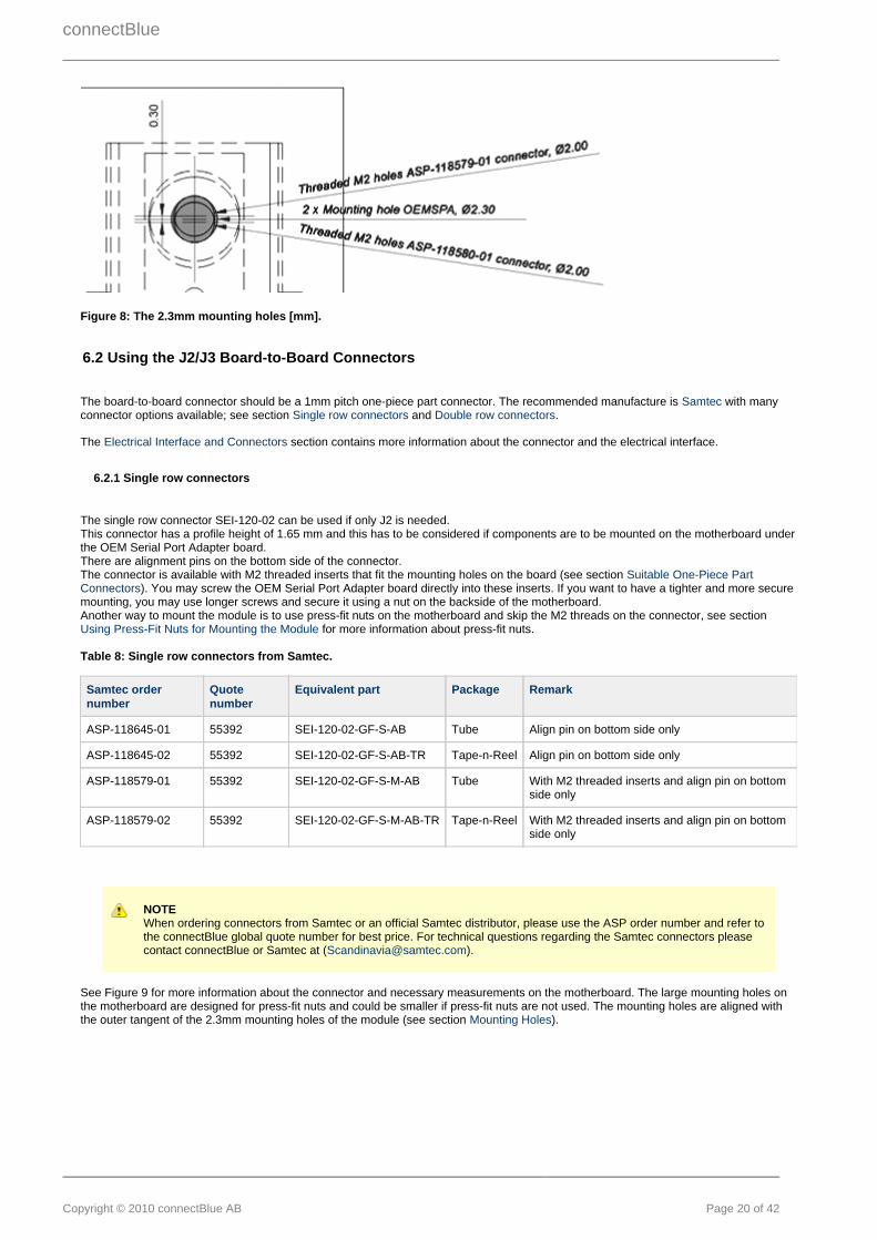
There are 2 x 2.3mm mounting holes on the cB-OBS411 module. The reasons for the 2.3mm holes are that the threaded M2 holes on thesingle and double row connectors (see section ) are not aligned. The outer tangents of the 2.3mmSuitable One-Piece Part Connectorsholes align the module if the single row connectors are used and the inner if double row connectors are used (see Figure 8).Choose the outer tangent (CC distance 27.24mm) if the module is aligned and mounted with some other technique based on M2 screws(e.g. press-fit nuts), see Figure 9 and Figure 10.
connectBlue
Copyright © 2010 connectBlue AB Page 20 of 42
Figure 8: The 2.3mm mounting holes [mm].
6.2 Using the J2/J3 Board-to-Board Connectors
The board-to-board connector should be a 1mm pitch one-piece part connector. The recommended manufacture is with manySamtecconnector options available; see section and .Single row connectors Double row connectors
The section contains more information about the connector and the electrical interface.Electrical Interface and Connectors
6.2.1 Single row connectors
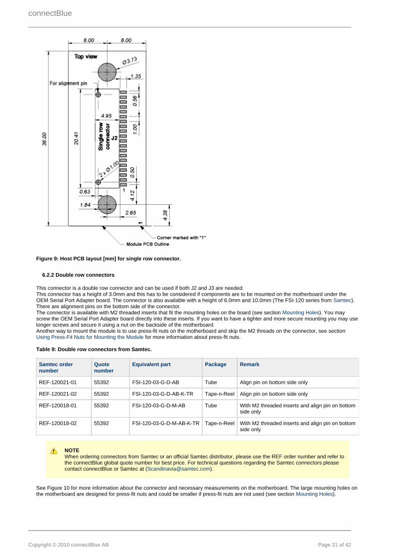
The single row connector SEI-120-02 can be used if only J2 is needed.This connector has a profile height of 1.65 mm and this has to be considered if components are to be mounted on the motherboard underthe OEM Serial Port Adapter board.There are alignment pins on the bottom side of the connector.The connector is available with M2 threaded inserts that fit the mounting holes on the board (see section Suitable One-Piece Part
). You may screw the OEM Serial Port Adapter board directly into these inserts. If you want to have a tighter and more secureConnectorsmounting, you may use longer screws and secure it using a nut on the backside of the motherboard.Another way to mount the module is to use press-fit nuts on the motherboard and skip the M2 threads on the connector, see section
for more information about press-fit nuts.Using Press-Fit Nuts for Mounting the Module
Table 8: Single row connectors from Samtec.
Samtec ordernumber
Quotenumber
Equivalent part Package Remark
ASP-118645-01 55392 SEI-120-02-GF-S-AB Tube Align pin on bottom side only
ASP-118645-02 55392 SEI-120-02-GF-S-AB-TR Tape-n-Reel Align pin on bottom side only
ASP-118579-01 55392 SEI-120-02-GF-S-M-AB Tube With M2 threaded inserts and align pin on bottomside only
ASP-118579-02 55392 SEI-120-02-GF-S-M-AB-TR Tape-n-Reel With M2 threaded inserts and align pin on bottomside only
NOTEWhen ordering connectors from Samtec or an official Samtec distributor, please use the ASP order number and refer tothe connectBlue global quote number for best price. For technical questions regarding the Samtec connectors pleasecontact connectBlue or Samtec at ( )[email protected]
See Figure 9 for more information about the connector and necessary measurements on the motherboard. The large mounting holes onthe motherboard are designed for press-fit nuts and could be smaller if press-fit nuts are not used. The mounting holes are aligned withthe outer tangent of the 2.3mm mounting holes of the module (see section ).Mounting Holes
connectBlue
Copyright © 2010 connectBlue AB Page 21 of 42
Figure 9: Host PCB layout [mm] for single row connector.
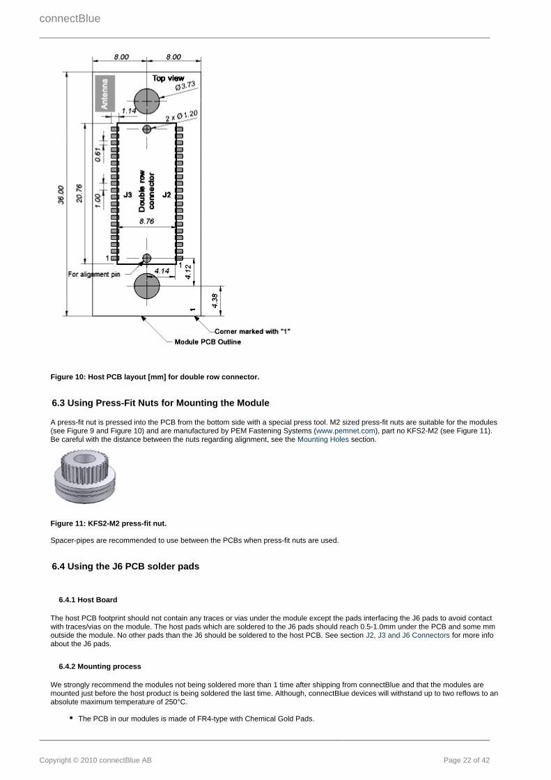
6.2.2 Double row connectors
This connector is a double row connector and can be used if both J2 and J3 are needed.This connector has a height of 3.0mm and this has to be considered if components are to be mounted on the motherboard under theOEM Serial Port Adapter board. The connector is also available with a height of 6.0mm and 10.0mm (The FSI-120 series from ).SamtecThere are alignment pins on the bottom side of the connector.The connector is available with M2 threaded inserts that fit the mounting holes on the board (see section ). You mayMounting Holesscrew the OEM Serial Port Adapter board directly into these inserts. If you want to have a tighter and more secure mounting you may uselonger screws and secure it using a nut on the backside of the motherboard.Another way to mount the module is to use press-fit nuts on the motherboard and skip the M2 threads on the connector, see section
for more information about press-fit nuts.Using Press-Fit Nuts for Mounting the Module
Table 9: Double row connectors from Samtec.
Samtec ordernumber
Quotenumber
Equivalent part Package Remark
REF-120021-01 55392 FSI-120-03-G-D-AB Tube Align pin on bottom side only
REF-120021-02 55392 FSI-120-03-G-D-AB-K-TR Tape-n-Reel Align pin on bottom side only
REF-120018-01 55392 FSI-120-03-G-D-M-AB Tube With M2 threaded inserts and align pin on bottomside only
REF-120018-02 55392 FSI-120-03-G-D-M-AB-K-TR Tape-n-Reel With M2 threaded inserts and align pin on bottomside only
NOTEWhen ordering connectors from Samtec or an official Samtec distributor, please use the REF order number and refer tothe connectBlue global quote number for best price. For technical questions regarding the Samtec connectors pleasecontact connectBlue or Samtec at ( )[email protected]
See Figure 10 for more information about the connector and necessary measurements on the motherboard. The large mounting holes onthe motherboard are designed for press-fit nuts and could be smaller if press-fit nuts are not used (see section ).Mounting Holes
connectBlue
Copyright © 2010 connectBlue AB Page 22 of 42
Figure 10: Host PCB layout [mm] for double row connector.
6.3 Using Press-Fit Nuts for Mounting the Module
A press-fit nut is pressed into the PCB from the bottom side with a special press tool. M2 sized press-fit nuts are suitable for the modules(see Figure 9 and Figure 10) and are manufactured by PEM Fastening Systems ( ), part no KFS2-M2 (see Figure 11).www.pemnet.comBe careful with the distance between the nuts regarding alignment, see the section. Mounting Holes
Figure 11: KFS2-M2 press-fit nut.
Spacer-pipes are recommended to use between the PCBs when press-fit nuts are used.
6.4 Using the J6 PCB solder pads
6.4.1 Host Board
The host PCB footprint should not contain any traces or vias under the module except the pads interfacing the J6 pads to avoid contactwith traces/vias on the module. The host pads which are soldered to the J6 pads should reach 0.5-1.0mm under the PCB and some mmoutside the module. No other pads than the J6 should be soldered to the host PCB. See section for more infoJ2, J3 and J6 Connectorsabout the J6 pads.
6.4.2 Mounting process
We strongly recommend the modules not being soldered more than 1 time after shipping from connectBlue and that the modules aremounted just before the host product is being soldered the last time. Although, connectBlue devices will withstand up to two reflows to anabsolute maximum temperature of 250°C.
The PCB in our modules is made of FR4-type with Chemical Gold Pads.
connectBlue
Copyright © 2010 connectBlue AB Page 23 of 42
The modules are produced in a lead-free process with a lead-free soldering paste.It is recommended that the customers make their own electrical, climate, stress and vibration tests on the final assembledproduct to secure that the manufacturing process hasn't damaged or affected the Bluetooth module in any way.The modules are normally delivered without labels on each module when packaged on tape-and-reel. However, if they aredelivered with labels on each module, the labels should be removed before the module is processed since the labels do notwithstand the heat of soldering.Modules delivered on trays are classed with MSL-Class 3.The device recommended maximum re-flow temperature is 245°C for 10 sec.The device absolute maximum re-flow temperature is 250°C for 3 sec.
6.5 Antenna Issues
The unit cannot be mounted arbitrary, because of the radio communication. The unit with an internal surface mounted antenna(cB-OBS411i and cB-OBS411j) cannot be mounted in a metal enclosure. No metal casing or plastics using metal flakes should be used,avoid also metallic based paint or lacquer. Keep a minimum clearance of 5 mm between the antenna and the casing. Keep minimum 10mm free space from metal around the antenna including under and above. If a metal enclosure is required, one of the external antennaoptions has to be used. See for more information on the antenna options available.Surface Mounted Antenna (Internal)
connectBlue
Copyright © 2010 connectBlue AB Page 24 of 42
7 Bluetooth Information
7.1 General information
In the tables below you can find information about Bluetooth properties. The output power of the cB-OBS411 device is max +4dBm(2.5mW).
Table 10: Bluetooth information cB-OBS411
Parameter Data
Bluetooth radio ST-Ericsson STLC2500DB
Host micro controller ST Microelectronics STM32F10x
RF output power (conducted - excluding antenna gain)
Class 1, max 4dBm
Receive sensitive level -84dBm
Receive input level (max) +15dBm
Output frequency 2.402 - 2.480 GHz, ISM band.
Bluetooth stack connectBlue Embedded Bluetooth Stack
Bluetooth qualification 2.1+EDR
7.2 Bluetooth Qualification information
All products based on the PCB cB-0925 have been qualified according to the Bluetooth specification 2.1+EDR.
Table 11: Bluetooth Qualification information
Module Bluetooth specification Referenced QDIDs List date (EPL)
cB-OBS411 2.1+ EDR B016013 combined with B015102 2009-10-26
The following Bluetooth profiles are supported (covered functionality):
Generic Access Profile (GAP)Serial Port Profile (SPP)Dial-up Networking Profile (DUN GW, DUN DT)
When creating end products based on the cB-OBS411 the following applies:
The end product does not have to be re-tested or re-qualified.A free of charge Bluetooth End Product Listing (EPL) be completed at the Bluetooth SIG website www.bluetooth.org. Thismustapplies for all products implementing Bluetooth technology. The EPL requires no testing (online listing only) and is goodmarketing since the product is published at the Bluetooth web site www.bluetooth.com. A free of charge "Adopter Bluetooth SIGmembership" is required.Create the EPL based on the connectBlue cB-OBH411 (QD ID: B016013) combined with the connectBlue Embedded BluetoothHost Stack (QD ID:B015102). A guide describing each step in the end product listing process is available in the connectBlue
.Bluetooth Qualification GuideThe Bluetooth Trademark may be placed on the end product. This requires a free of charge Adopter Bluetooth SIG membership.For more information see www.bluetooth.orgThe Bluetooth Trademark may be used in material related to the end product. This requires a free of charge Adopter BluetoothSIG membership. For more information see .www.bluetooth.org

connectBlue
Copyright © 2010 connectBlue AB Page 25 of 42
For more information please contact .connectBlue
connectBlue
Copyright © 2010 connectBlue AB Page 26 of 42
8 Regulatory Information
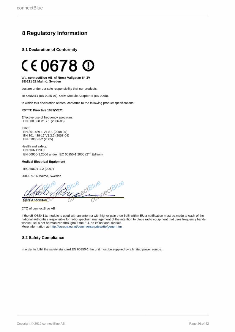
8.1 Declaration of Conformity
We, , of connectBlue AB Norra Vallgatan 64 3VSE-211 22 Malmö, Sweden
declare under our sole responsibility that our products:
cB-OBS411 (cB-0925-01), OEM Module Adapter III (cB-0068).
to which this declaration relates, conforms to the following product specifications:
R&TTE Directive 1999/5/EC:
Effective use of frequency spectrum: EN 300 328 V1.7.1 (2006-05)
EMC: EN 301 489-1 V1.8.1 (2008-04) EN 301 489-17 V1.3.2 (2008-04) EN 61000-6-2 (2005)
Health and safety: EN 50371:2002 EN 60950-1:2006 and/or IEC 60950-1:2005 (2 Edition)nd
Medical Electrical Equipment
IEC 60601-1-2 (2007)
2009-09-16 Malmö, Sweden
CTO of connectBlue AB
If the cB-OBS411x module is used with an antenna with higher gain then 5dBi within EU a notification must be made to each of thenational authorities responsible for radio spectrum management of the intention to place radio equipment that uses frequency bandswhose use is not harmonized throughout the EU, on its national market.More information at: http://europa.eu.int/comm/enterprise/rtte/gener.htm
8.2 Safety Compliance
In order to fulfill the safety standard EN 60950-1 the unit must be supplied by a limited power source.
connectBlue
Copyright © 2010 connectBlue AB Page 27 of 42
8.3 FCC and IC Compliance
See the section for information about the different product variants.Product Variants
8.3.1 Compliance for cB-0925
8.3.1.1 FCC Statement for cB-0925
This device complies with Part 15 of the FCC Rules. Operation is subject to the following two conditions:
(1) this device may not cause harmful interference, and(2) this device must accept any interference received, including interference that may cause undesired operation.
NOTEThis equipment has been tested and found to comply with the limits for a Class B digital device, pursuant to Part 15 ofthe FCC Rules. These limits are designed to provide reasonable protection against harmful interference in a residentialinstallation. This equipment generates, uses and can radiate radio frequency energy and, if not installed and used inaccordance with the instructions, may cause harmful interference to radio communications. However, there is noguarantee that interference will not occur in a particular installation. If this equipment does cause harmful interference toradio or television reception, which can be determined by turning the equipment off and on, the user is encouraged totry to correct the interference by one or more of the following measures:
Reorient or relocate the receiving antennaIncrease the separation between the equipment and receiverConnect the equipment into an outlet on a circuit different from that to which the receiver is connected
Consult the dealer or an experienced radio/TV technician for help.
8.3.1.2 Caution
Any changes or modifications NOT explicitly APPROVED by connectBlue AB could cause the module to cease to comply with FCC rulespart 15, and thus void the user's authority to operate the equipment.
8.3.1.3 IC Compliance
Operation is subject to the following two conditions:
(1) this device may not cause harmful interference, and(2) this device must accept any interference received,
including interference that may cause undesired operation.
This device has been designed to operate with an antenna having a maximum gain of 8.0 dBi.Having a higher gain is strictly prohibited per regulations of Industry Canada. The required antenna impedance is 50 ohms.To reduce potential radio interference to other users, the antenna type and its gain should be so chosen that the equivalent isotropicallyradiated power (EIRP) is not more than that required for successful communication.
The installer of this radio equipment must ensure that the antenna is located or pointed such that it does not emit RF field in excess ofHealth Canada limits for the general population; consult Safety Code 6, obtainable from Health Canada's website www.hc-sc.gc.ca/rpb
8.3.1.4 Labeling Requirements for End Product
For an end product using the product cB-0925 there must be a label containing, at least, the following information:
This device contains
FCC ID: PVH0925 IC: 5325A-0925
The label must be affixed on an exterior surface of the end product such that it will be visible upon inspection in compliance with themodular approval guidelines developed by the FCC.
In accordance with 47 CFR § 15.19 the end product shall bear the following statement in a conspicuous location on the device:
"This device complies with Part 15 of the FCC Rules.Operation is subject to the following two conditions;
(1) this device may not cause harmful interference, and
connectBlue
Copyright © 2010 connectBlue AB Page 28 of 42
(2) this device must accept any interference received, including interference that may cause undesired operation."
When the device is so small or for such use that it is not practicable to place the statement above on it, the information shall be placed ina prominent location in the instruction manual or pamphlet supplied to the user or, alternatively, shall be placed on the container in whichthe device is marketed. However, the FCC ID label must be displayed on the device.
In case, where the final product will be installed in locations where the end-user is not able to see the FCC ID and/or this statement, theFCC ID and the statement shall also be included in the end-product manual.
8.4 UL listing information
If a customer intends to UL list a product including any of the Bluetooth modules based on the PCB cB-0925 this information is useful:
The printed circuit board if produced according to the following specification:
UL recognized ZPMV2 min. 105 °C flame class V-0 or better.
8.5 Compliance with RoHS directive
All products based on the PCB cB-0925 are produced according to the RoHS (Restriction of the use of certain Hazardous substances inelectrical and electronic equipment) directive and complies with the directive.
connectBlue
Copyright © 2010 connectBlue AB Page 29 of 42
9 Guidelines for Efficient and Safe Use
9.1 General
Read this information before using your OEM Serial Port Adapter.
For any exceptions, due to national requirements or limitations, when using your OEM Serial Port Adapter, please visitwww.bluetooth.org.
NOTEChanges or modifications to the product not expressly approved by connectBlue AB will void the user's authority tooperate the equipment.
9.2 Product Care
Do not expose your product to liquid or moisture.Do not expose you product to extreme hot or cold temperature (see section for further information).EnvironmentalDo not expose your product to lit candles, cigarettes, cigars, open flames, etc.Do not drop, throw or try to bend your product since rough treatment could damage your product.Do not attempt to disassemble your product. Doing so will void warranty. The product does not contain consumer serviceable orreplaceable components. Service should only be performed by connectBlue AB.Do not paint your product as the paint could prevent normal use.If you will not be using your product for a while, store it in a place that is dry, free from damp, dust and extreme heat and cold.The clearance and creepage distances required by the end product must be withheld when the module is installed.The cooling of the end product shall not negatively be influenced by the installation of the module when the module is installed.
9.3 Radio Frequency Exposure
The OEM Serial Port Adapter contains a small radio transmitter and receiver. During communication with other Bluetooth products theOEM Serial Port Adapter receives and transmits radio frequency (RF) electromagnetic fields (microwaves) in the frequency range 2400 to2500 MHz. The output power of the radio transmitter is less than 4mW.
When using the OEM Serial Port Adapter, you will be exposed to some of the transmitted RF energy. This exposure is well below theprescribed limits in all national and international RF safety standards and regulations.
9.4 Electronic Equipment
Most modern electronic equipment, for example, in hospitals and cars, is shielded from RF energy. However, certain electronicequipment is not. Therefore:
NOTEThis equipment emits RF energy in the ISM (Industrial, Scientific, Medical) band. Please insure that all medical devicesused in proximity to this device meet appropriate susceptibility specifications for this type of RF energy.
9.5 Potentially Explosive Atmospheres
Turn off your electronic device before entering an area with potentially explosive atmosphere. It is rare, but your electronic device couldgenerate sparks. Sparks in such areas could cause an explosion or fire resulting in bodily injury or even death.
Areas with a potentially explosive atmosphere are often, but not always, clearly marked. They include fuelling areas, such as petrolstation, below deck on boats, fuel or chemical transfer or storage facilities, and areas where the air contains chemicals or particles, suchas grain, dust, or metal powders.
9.6 Power Supply
The OEM Serial Port Adapter must be supplied by a limited power source according to EN 60950-1.
Connect your power supply only to designated power-sources as marked on the product.Make sure all cords and cable are positioned so that they will not be stepped on, tripped over or otherwise subject to damage orstress.To reduce risk of electric shock, unplug the unit from any power source before attempting to clean it.
connectBlue
Copyright © 2010 connectBlue AB Page 30 of 42
10 Application Notes
Usually only a subset of the available functionality is of interest to the designer. In addition, depending on the host system, the electricalinterface can be designed in many ways. The designer can use the step-by-step guide in this chapter as an aid in the design process.
10.1 Step-by-Step Guide
Table 12: Step-by-step guide with Yes and No answers.
Question Yes No
Are you going to integrate the OEMSerial Port Adapter in a metalenclosure?
Use one of the OEM Serial Ports Adapters withantenna connector for external antenna(cB-OBS411x).
Go on to next point.
Do you wish to use logic level whencommunicating with the OEM Serial PortAdapter?
See section for electrical design.Logic level Mode See section External RS232 driverand forExternal RS422 driverelectrical design.
Do you want to use RS232 as thephysical serial interface?
See section for electricalExternal RS232 driverdesign.
Go on to next point.
Do you wish to connect LEDs to theOEM Serial Port Adapter?
See section for designLED and Switch Designexamples for connecting the LEDs.
Go on to next point.
Do you want to detect the status of themodule with a controller?
See section for status detectionOperating Statusand section for electricalLED and Switch Designdesign.
Go on to next point.
Do you wish to utilize the restore switch? See section for electrical design.GREEN/Switch-1 Go on to next point.
Do you wish to utilize the Functionswitch ("Connect on external signal")?
See section for electrical design.Switch-0 Signal Go on to next point.
Do you want to manually reset themodule?
See section for electrical design. Use aResetdouble row connector. See section Double row
.connectors
10.2 Design Examples
This section contains design examples for all interfaces on J2, J3, and J6. The connector type that suits a specific application depends onthe needed signal and the preferred interface type (board-to-board or SMD).
10.2.1 Logic Levels
10.2.1.1 3.0/3.3 voltage host system
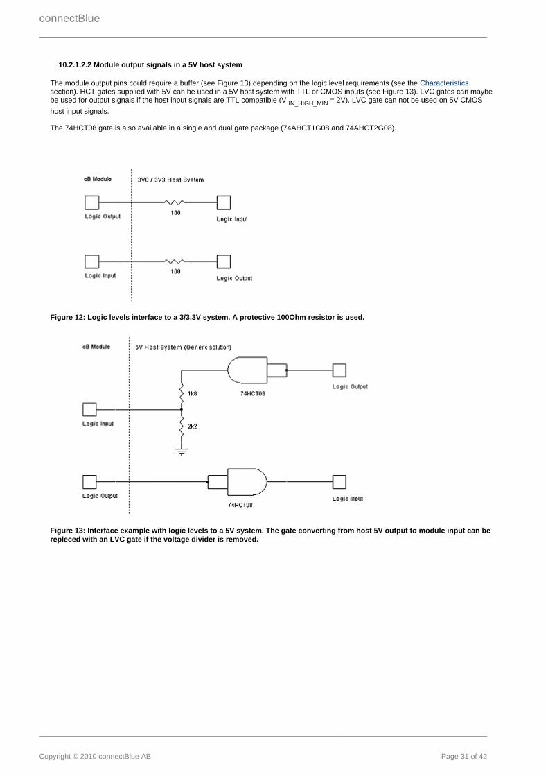
A 3.0/3.3V host system can be connected directly to the logic level pins (BLUE, UART-TxD / UART-RxD etc). A serial 100Ohm resistorshall be used (see Figure 12) for protection, see the section for logic levels characteristics.Characteristics
10.2.1.2 5 voltage host system
A 5V host system can easily be adjusted to the logic levels.
10.2.1.2.1 Module input signals in a 5V host system
The module input signals can use a resistive divider (1.8kOhm/2.2kOhm) to adjust the levels (See Figure 12). This is applicable forspeeds up to 115.2kBits/s. The divider can be improved by adding a logic buffer (74HCT08) for higher speeds (see Figure 13). Theresistor dividers consume current and a better solution could be to use the 5V input tolerant gates in the LVC family. The LVC gates areavailable in singel, dual and quad gates packages (e.g. 74LVC1G08, 74LVC2G08 and 74LVC08). The LVC gates need to be powersupplied with the module signal voltage levels (see ). The VCC_2V85 pin (see the section) can beInput/Output signals Pin Descriptionused for suppling the interface circuits. Notice that the VCC_2V85 output voltage supply not is available on all connectBlue modules e.g.if the application is designed to be used with different pin compatible connectBlue modules.
The LVC gates could maybe also be used for output signals if the host input signals are TTL compatible (V = 2V). LVC gateIN_HIGH_MINcan not be used on 5V CMOS input signals.
connectBlue
Copyright © 2010 connectBlue AB Page 31 of 42
10.2.1.2.2 Module output signals in a 5V host system
The module output pins could require a buffer (see Figure 13) depending on the logic level requirements (see the Characteristicssection). HCT gates supplied with 5V can be used in a 5V host system with TTL or CMOS inputs (see Figure 13). LVC gates can maybebe used for output signals if the host input signals are TTL compatible (V = 2V). LVC gate can not be used on 5V CMOSIN_HIGH_MINhost input signals.
The 74HCT08 gate is also available in a single and dual gate package (74AHCT1G08 and 74AHCT2G08).
Figure 12: Logic levels interface to a 3/3.3V system. A protective 100Ohm resistor is used.
Figure 13: Interface example with logic levels to a 5V system. The gate converting from host 5V output to module input can berepleced with an LVC gate if the voltage divider is removed.
connectBlue
Copyright © 2010 connectBlue AB Page 32 of 42
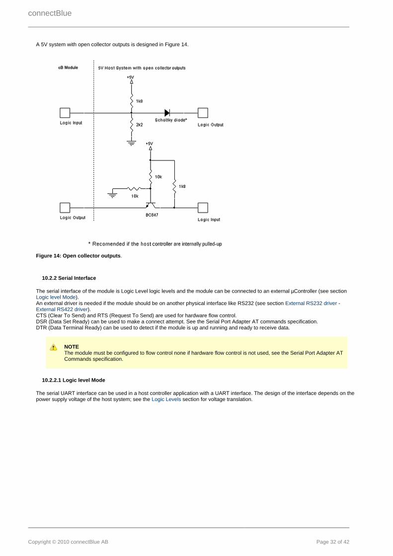
A 5V system with open collector outputs is designed in Figure 14.
. Figure 14: Open collector outputs
10.2.2 Serial Interface
The serial interface of the module is Logic Level logic levels and the module can be connected to an external µController (see section ).Logic level Mode
An external driver is needed if the module should be on another physical interface like RS232 (see section - External RS232 driver).External RS422 driver
CTS (Clear To Send) and RTS (Request To Send) are used for hardware flow control.DSR (Data Set Ready) can be used to make a connect attempt. See the Serial Port Adapter AT commands specification.DTR (Data Terminal Ready) can be used to detect if the module is up and running and ready to receive data.
NOTEThe module must be configured to flow control none if hardware flow control is not used, see the Serial Port Adapter ATCommands specification.
10.2.2.1 Logic level Mode
The serial UART interface can be used in a host controller application with a UART interface. The design of the interface depends on thepower supply voltage of the host system; see the section for voltage translation.Logic Levels
connectBlue
Copyright © 2010 connectBlue AB Page 33 of 42
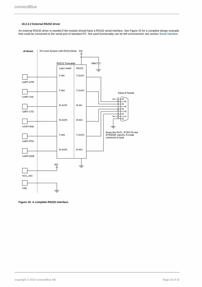
10.2.2.2 External RS232 driver
An external RS232 driver is needed if the module should have a RS232 serial interface. See Figure 15 for a complete design examplethat could be connected to the serial port of standard PC. Not used functionality can be left unconnected; see section .Serial Interface
Figure 15: A complete RS232 interface.
connectBlue
Copyright © 2010 connectBlue AB Page 34 of 42
10.2.2.3 External RS422 driver
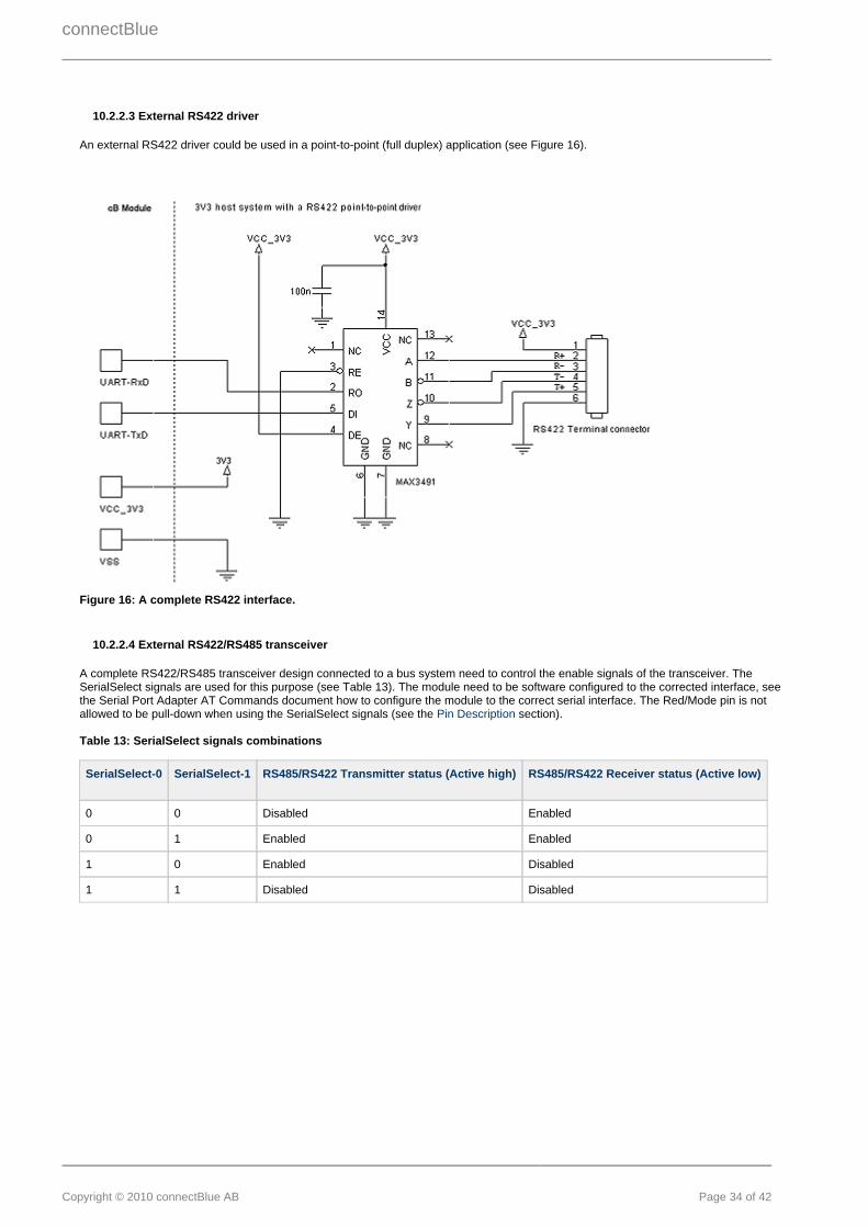
An external RS422 driver could be used in a point-to-point (full duplex) application (see Figure 16).
Figure 16: A complete RS422 interface.
10.2.2.4 External RS422/RS485 transceiver
A complete RS422/RS485 transceiver design connected to a bus system need to control the enable signals of the transceiver. TheSerialSelect signals are used for this purpose (see Table 13). The module need to be software configured to the corrected interface, seethe Serial Port Adapter AT Commands document how to configure the module to the correct serial interface. The Red/Mode pin is notallowed to be pull-down when using the SerialSelect signals (see the section).Pin Description
Table 13: SerialSelect signals combinations
erialSelect-0S SerialSelect-1 RS485/RS422 Transmitter status (Active high) RS485/RS422 Receiver status (Active low)
0 0 Disabled Enabled
0 1 Enabled Enabled
1 0 Enabled Disabled
1 1 Disabled Disabled
connectBlue
Copyright © 2010 connectBlue AB Page 35 of 42
Figure 17: A complete RS422/RS485 transceiver design.
10.2.3 LED and Switch Design
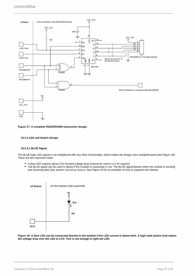
10.2.3.1 BLUE Signal
The BLUE logic LED signal is not multiplexed with any other functionality, which makes the design more straightforward (see Figure 18).There are two important notes:
A blue LED requires about 3.5V forward voltage drop (cannot be used in a 3.3V system).The BLUE signal can be used to detect if the module is connected or not. The BLUE signal flashes when the module is sendingand receiving data (see section ). See Figure 19 for an example on how to suppress the flashes.Operating Status
Figure 18: A blue LED can be connected directly to the module if the LED current is below 4mA. A high state (active low) makes the voltage drop over the LED to 2.2V. This is not enough to light the LED.
connectBlue
Copyright © 2010 connectBlue AB Page 36 of 42
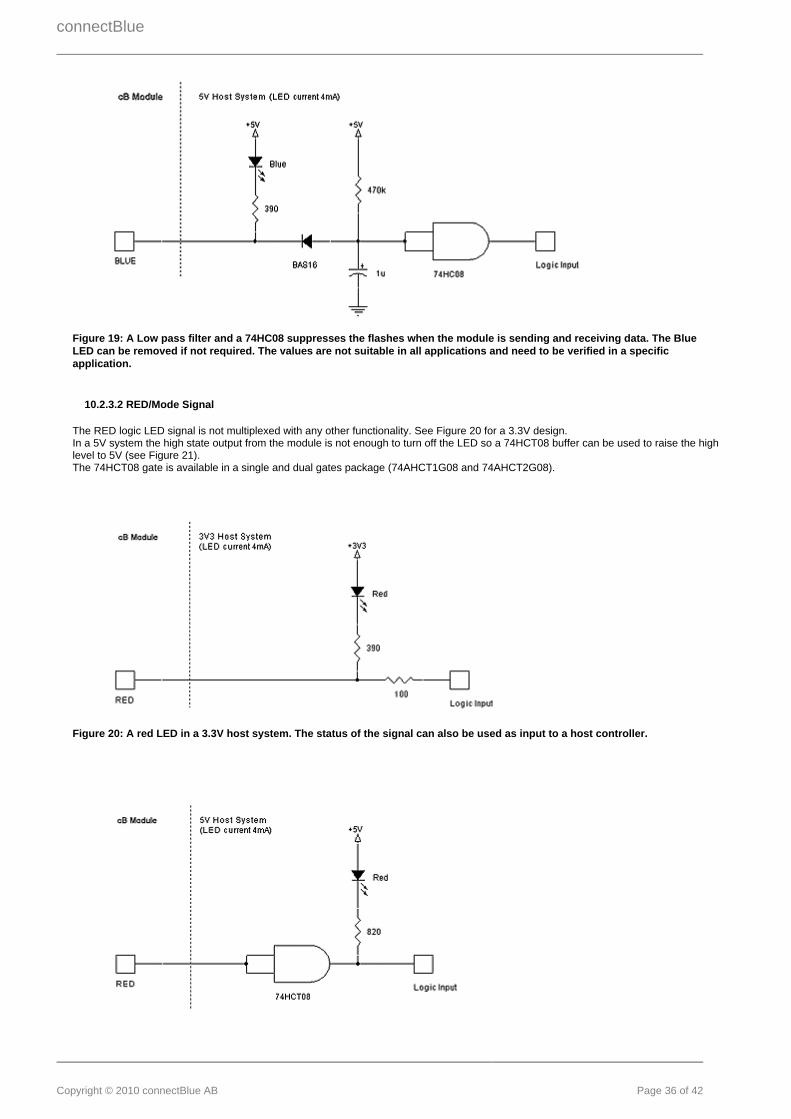
Figure 19: A Low pass filter and a 74HC08 suppresses the flashes when the module is sending and receiving data. The BlueLED can be removed if not required. The values are not suitable in all applications and need to be verified in a specific
application.
10.2.3.2 RED/Mode Signal
The RED logic LED signal is not multiplexed with any other functionality. See Figure 20 for a 3.3V design.In a 5V system the high state output from the module is not enough to turn off the LED so a 74HCT08 buffer can be used to raise the highlevel to 5V (see Figure 21).The 74HCT08 gate is available in a single and dual gates package (74AHCT1G08 and 74AHCT2G08).
Figure 20: A red LED in a 3.3V host system. The status of the signal can also be used as input to a host controller.
connectBlue
Copyright © 2010 connectBlue AB Page 37 of 42
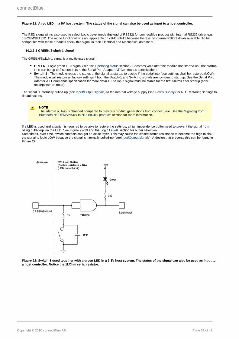
Figure 21: A red LED in a 5V host system. The status of the signal can also be used as input to a host controller.
The RED signal pin is also used to select Logic Level mode (instead of RS232) for connectBlue product with internal RS232 driver e.g.cB-OEMSPA312. The mode functionality is not applicable on cB-OBS411 because there is no internal RS232 driver available. To becompatible with these products check this signal in their Electrical and Mechanical datasheet.
10.2.3.3 GREEN/Switch-1 signal
The GREEN/Switch-1 signal is a multiplexed signal:
GREEN - Logic green LED signal (see the section). Becomes valid after the module has started up. The startupOperating statustime can be up to 2 seconds (see the Serial Port Adapter AT Commands specification).Switch-1 - The module reads the status of the signal at startup to decide if the serial interface settings shall be restored (LOW).The module will restore all factory settings if both the Switch-1 and Switch-0 signals are low during start up. See the Serial PortAdapter AT Commands specification for more details. The input signal must be stable for the first 500ms after startup (afterreset/power on reset).
The signal is internally pulled-up (see ) to the internal voltage supply (see ) for NOT restoring settings toInput/Output signals Power supplydefault values.
NOTEThe internal pull-up is changed compared to previous product generations from connectBlue. See the Migrating from
section for more information.Bluetooth cB-OEMSPA3xx to cB-OBS4xx products
If a LED is used and a switch is required to be able to restore the settings, a high impendence buffer need to prevent the signal frombeing pulled-up via the LED. See Figure 22-23 and the section for buffer selection.Logic LevelsSometimes, over time, switch contacts can get an oxide layer. This may cause the closed switch resistance to become too high to sinkthe signal to logic LOW because the signal is internally pulled-up (see ). A design that prevents this can be found inInput/Output signalsFigure 27.
Figure 22: Switch-1 used together with a green LED in a 3.3V host system. The status of the signal can also be used as input to a host controller. Notice the 1kOhm serial resistor.

connectBlue
Copyright © 2010 connectBlue AB Page 38 of 42
Figure 23: Switch-1 used together with a green LED in a 5V host system. The status of the signal can also be used as input to a host controller. Notice the 1kOhm serial resistor.
The buffer can be removed in a 3.3V system if no restore switch is required (see Figure 24).
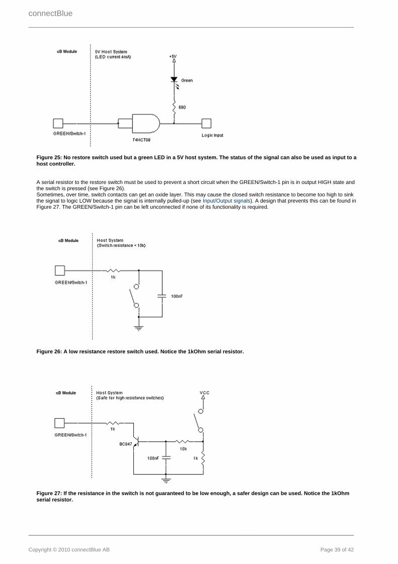
In a 5V system the high state output from the module is not enough to turn off the LED, so a 74HCT08 buffer can be used to raise thehigh level to 5V (see Figure 25).The 74HCT08 gate is also available in a single gate package (74AHCT1G08).
Figure 24: No restore switch used but a green LED in a 3.3V host system. The status of the signal can also be used as input to a host controller.
connectBlue
Copyright © 2010 connectBlue AB Page 39 of 42
Figure 25: No restore switch used but a green LED in a 5V host system. The status of the signal can also be used as input to a host controller.
A serial resistor to the restore switch must be used to prevent a short circuit when the GREEN/Switch-1 pin is in output HIGH state andthe switch is pressed (see Figure 26).Sometimes, over time, switch contacts can get an oxide layer. This may cause the closed switch resistance to become too high to sinkthe signal to logic LOW because the signal is internally pulled-up (see ). A design that prevents this can be found inInput/Output signalsFigure 27. The GREEN/Switch-1 pin can be left unconnected if none of its functionality is required.
Figure 26: A low resistance restore switch used. Notice the 1kOhm serial resistor.
Figure 27: If the resistance in the switch is not guaranteed to be low enough, a safer design can be used. Notice the 1kOhm serial resistor.
connectBlue
Copyright © 2010 connectBlue AB Page 40 of 42
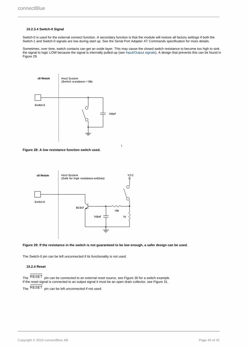
10.2.3.4 Switch-0 Signal
Switch-0 is used for the external connect function. A secondary function is that the module will restore all factory settings if both theSwitch-1 and Switch-0 signals are low during start up. See the Serial Port Adapter AT Commands specification for more details.
Sometimes, over time, switch contacts can get an oxide layer. This may cause the closed switch resistance to become too high to sinkthe signal to logic LOW because the signal is internally pulled-up (see ). A design that prevents this can be found inInput/Output signalsFigure 29.
\ Figure 28: A low resistance function switch used.
Figure 29: If the resistance in the switch is not guaranteed to be low enough, a safer design can be used.
The Switch-0 pin can be left unconnected if its functionality is not used.
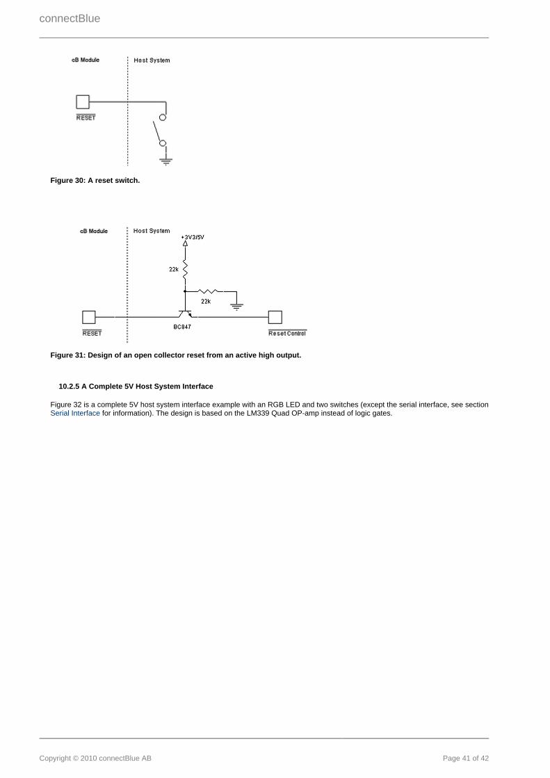
10.2.4 Reset
The pin can be connected to an external reset source, see Figure 30 for a switch example.If the reset signal is connected to an output signal it must be an open drain collector, see Figure 31.
The pin can be left unconnected if not used.
connectBlue
Copyright © 2010 connectBlue AB Page 41 of 42
Figure 30: A reset switch.
Figure 31: Design of an open collector reset from an active high output.
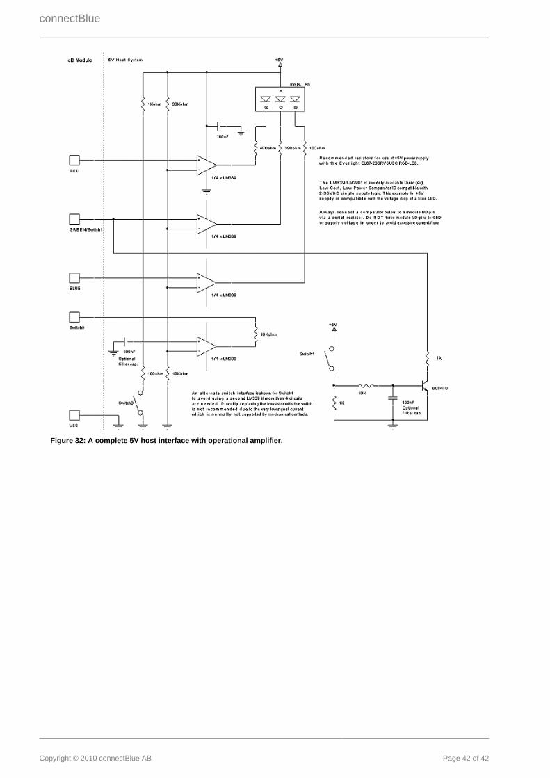
10.2.5 A Complete 5V Host System Interface
Figure 32 is a complete 5V host system interface example with an RGB LED and two switches (except the serial interface, see section for information). The design is based on the LM339 Quad OP-amp instead of logic gates.Serial Interface
connectBlue
Copyright © 2010 connectBlue AB Page 42 of 42
Figure 32: A complete 5V host interface with operational amplifier.