c:/documents and settings/ccsun/®à ±/paper/phd/diss
TRANSCRIPT

VLSI Design Concepts for Iterative Algorithms
Von der Fakultat fur Elektrotechnik und Informationstechnik
der Technischen Universitat Dortmund
genehmigte
Dissertation
zur Erlangung des akademischen Grades
Doktor der Ingenieurwissenschaften
eingereicht von
Chi-Chia Sun
Tag der mundlichen Prufung: 11.04.2011
Hauptreferent: Univ.-Prof. Dr.-Ing. Jurgen Gotze
Korreferent: Univ.-Prof. Dr.-Ing. Rudiger Kays
Arbeitsgebiet Datentechnik, Technische Universitat Dortmund

Abstract
Circuit design becomes more and more complicated, especially whenthe Very Large Scale Integration (VLSI) manufacturing technology nodekeeps shrinking down to nanoscale level. New challenges come up suchas an increasing gap between the design productivity and the Moore’sLaw. Leakage power becomes a major factor of the power consumptionand traditional shared bus transmission is the critical bottleneck in thebillion transistors Multi-Processor System–on–Chip (MPSoC) designs.These issues lead us to discuss the impact on the design of iterativealgorithms.
This thesis presents several strategies that satisfy various design con-straints, which can be used to explore superior solutions for the circuitdesign of iterative algorithms. Four selected examples of iterative al-gorithms are elaborated in this respect: hardware implementation ofCOordinate Rotation DIgital Computer (CORDIC) processor for sig-nal processing, configurable DCT and integer transformations basedCORDIC algorithm for image/video compression, parallel Jacobi Eigen-value Decomposition (EVD) method with arbitrary iterations for com-munication, and acceleration of parallel Sparse Matrix–Vector Multipli-cation (SMVM) operations based Network–on–Chip (NoC) for solvingsystems of linear equations. These four applications of iterative meth-ods have been chosen since they cover a wide area of current signalprocessing tasks.
Each method has its own unique design criteria when it comes tothe direct implementation on the circuit level. Therefore, a balancedsolution between various design tradeoffs is elaborated for each method.These tradeoffs are between throughput and power consumption, com-putational complexity and transformation accuracy, the number of in-ner/outer iterations and energy consumption, data structure and net-work topology. It is shown that all of these algorithms can be imple-mented on FPGA devices or as ASICs efficiently.


Acknowledgements
This thesis was written while I was working as a research assistant at theInformation Processing Laboratory of the Dortmund University of Tech-nology. I would like to thank Professor Dr.-Ing. Jurgen Gotze, the headof the laboratory, for all the interesting discussions that contributed es-sentially to this thesis, for creating an open and relaxed atmosphere,and for providing excellent working conditions.
Furthermore, I am very pleased to thank Professor Dr.-Ing. RudigerKays (TU Dortmund) for his interest in my works, his comments on mythesis and his reviews for my DAAD scholarship, and his time.
I would also like to thank Professor Shanq-Jang Ruan (Low-PowerSystem Lab, National Taiwan University of Science and Technology) forhis guidance during my Master study in Taipei. I am especially gratefulto my present and former colleagues for providing such a stimulatingatmosphere at the laboratory. It was a pleasure to share so much timewith you. Special thanks goes to many students for their contributionsto this work too.
To my parents and my sister for their support and encouragementsduring the long years of my education.
Dortmund Germany, April 2011


Contents
1 Introduction 1
2 Introduction to VLSI Design 92.1 Modern Digital Circuit Design . . . . . . . . . . . . . . . 92.2 Moore’s Law . . . . . . . . . . . . . . . . . . . . . . . . 112.3 Circuit Design Issues: Modular Design . . . . . . . . . . 122.4 Circuit Design Issues: Low Power . . . . . . . . . . . . . 162.5 Circuit Design Issues: Synthesis for Power Efficiency . . 172.6 Circuit Design Issues: Source of Power Dissipation . . . . 19
2.6.1 Dynamic Power Dissipation . . . . . . . . . . . . 202.6.2 Short Circuit Power Dissipation . . . . . . . . . . 212.6.3 Static Leakage Power Dissipation . . . . . . . . . 21
2.7 Design Consideration for Iterative Algorithms . . . . . . 232.8 Summary . . . . . . . . . . . . . . . . . . . . . . . . . . 24
3 CORDIC Algorithm 253.1 Generic CORDIC Algorithm . . . . . . . . . . . . . . . . 253.2 Extension to Linear and Hyperbolic functions . . . . . . 303.3 CORDIC in Hardware . . . . . . . . . . . . . . . . . . . 323.4 Hardware Performance Analysis . . . . . . . . . . . . . . 353.5 Summary . . . . . . . . . . . . . . . . . . . . . . . . . . 36
4 Discrete Cosine Integer Transform (DCIT) 374.1 Introduction of DCIT . . . . . . . . . . . . . . . . . . . . 374.2 DCT algorithms . . . . . . . . . . . . . . . . . . . . . . . 39
4.2.1 The DCT Background . . . . . . . . . . . . . . . 394.2.2 The CORDIC based Loeffler DCT . . . . . . . . . 404.2.3 4×4 Integer Transform . . . . . . . . . . . . . . . 424.2.4 8×8 Integer Transform . . . . . . . . . . . . . . . 43
4.3 Discrete Cosine and Integer Transform . . . . . . . . . . 464.3.1 Forward DCIT . . . . . . . . . . . . . . . . . . . 464.3.2 Inverse DCIT . . . . . . . . . . . . . . . . . . . . 48

4.4 The proposed 2–D QDCIT framework . . . . . . . . . . . 514.4.1 The 2–D QDCIT . . . . . . . . . . . . . . . . . . 514.4.2 The CORDIC based Scaler . . . . . . . . . . . . . 534.4.3 The CORDIC-Scaler Configurator and the LUT
Read Module . . . . . . . . . . . . . . . . . . . . 574.4.4 The Post-Quantizer . . . . . . . . . . . . . . . . . 61
4.5 Experimental Results . . . . . . . . . . . . . . . . . . . . 634.5.1 Variable Iteration Steps of CORDIC . . . . . . . 644.5.2 ASIC Implementation . . . . . . . . . . . . . . . 654.5.3 Performance in MPEG–4 XVID and H.264 . . . . 67
4.6 Summary . . . . . . . . . . . . . . . . . . . . . . . . . . 75
5 Parallel Jacobi Algorithm 775.1 Parallel Eigenvalue Decomposition . . . . . . . . . . . . 78
5.1.1 Jacobi Method . . . . . . . . . . . . . . . . . . . 785.1.2 Jacobi EVD Array . . . . . . . . . . . . . . . . . 79
5.2 Architecture Consideration . . . . . . . . . . . . . . . . . 815.2.1 Conventional CORDIC Solution . . . . . . . . . . 815.2.2 Simplified µ–rotation CORDIC . . . . . . . . . . 835.2.3 Adaptive µ–CORDIC iterations . . . . . . . . . . 855.2.4 Exchanging inner and outer iterations . . . . . . . 86
5.3 Experimental Results . . . . . . . . . . . . . . . . . . . . 875.3.1 Matlab Simulation . . . . . . . . . . . . . . . . . 875.3.2 Using threshold methods . . . . . . . . . . . . . . 895.3.3 Configurable Jacobi EVD Array . . . . . . . . . . 915.3.4 Circuit Implementation . . . . . . . . . . . . . . . 94
5.4 Summary . . . . . . . . . . . . . . . . . . . . . . . . . . 98
6 Sparse Matrix–Vector Multiplication on Network–on–Chip 1016.1 Introduction of Sparse Matrix–Vector Multiplication . . . 1026.2 SMVM on Network-on-Chip . . . . . . . . . . . . . . . . 103
6.2.1 Sparse Matrix-Vector Multiplication . . . . . . . 1036.2.2 Conjugate Gradient Solver . . . . . . . . . . . . . 1056.2.3 Basic Idea . . . . . . . . . . . . . . . . . . . . . . 106
6.3 Implementation . . . . . . . . . . . . . . . . . . . . . . . 1086.3.1 Packet Format . . . . . . . . . . . . . . . . . . . 1086.3.2 Switch Architecture . . . . . . . . . . . . . . . . . 1096.3.3 Pipelined Switch Architecture . . . . . . . . . . . 1116.3.4 Routing Algorithm . . . . . . . . . . . . . . . . . 1126.3.5 Processing Element . . . . . . . . . . . . . . . . . 113

6.3.6 Data Mapping . . . . . . . . . . . . . . . . . . . . 1136.4 Experimental Result . . . . . . . . . . . . . . . . . . . . 115
6.4.1 FPGA Implementation . . . . . . . . . . . . . . . 1156.4.2 Influence of the Sparsity . . . . . . . . . . . . . . 1166.4.3 Mapping to Iterative Solver . . . . . . . . . . . . 118
6.5 Summary . . . . . . . . . . . . . . . . . . . . . . . . . . 120
7 Conclusions 121
A Appendix Tables 125
B Appendix Figures 129
Bibliography 137


List of Figures
1.1 Designer productivity gap (modified from SEMATECH) 21.2 Iterative algorithm design concept . . . . . . . . . . . . . 3
2.1 Moore’s Law: Plot of x86 CPU transistor counts from1970 until 2010 . . . . . . . . . . . . . . . . . . . . . . . 11
2.2 IC scaling roadmap for More than Moore (modified figurefrom 2009 International Technology Roadmap for Semi-conductors Executive Summary) [58] . . . . . . . . . . . 13
2.3 Relative delays of interconnection wire and gate in nanoscalelevel (regenerated figure from International TechnologyRoadmap for Semiconductors 2003) [57] . . . . . . . . . 14
2.4 The prediction of future multi-core SoC performance (re-generated figure from 2009 International Technology Roadmapfor Semiconductors System Drivers) [59] . . . . . . . . . 15
2.5 A typical NoC architecture with a mesh style packet-switched network . . . . . . . . . . . . . . . . . . . . . . 16
2.6 Power reduction at each design level [88] . . . . . . . . . 182.7 A simple CMOS inverter . . . . . . . . . . . . . . . . . . 202.8 There are four components of leakage sources in NMOS:
Subthreshold leakage (ISub), Gate-oxide leakage (IGate),Reverse biased junction leakage (IRev) and Gate InducedDrain Leakage (IGIDL) . . . . . . . . . . . . . . . . . . . 22
3.1 CORDIC rotating and scaling a input vector < x0, y0 >in the orthogonal rotation mode . . . . . . . . . . . . . . 28
3.2 CORDIC rotating a input vector < x0, y0 > in the or-thogonal vector mode . . . . . . . . . . . . . . . . . . . . 29
3.3 Flow graph of a folded CORDIC (recursive) processor . . 333.4 Flow graph of an unfolded (parallel) CORDIC processor 343.5 Flow graph of an unfolded (parallel) CORDIC processor
with pipelining . . . . . . . . . . . . . . . . . . . . . . . 34
4.1 Flow graph of an 8–point Loeffler DCT architecture . . . 41
4.2 Flow graph of an 8–point CORDIC based Loeffler DCTarchitecture . . . . . . . . . . . . . . . . . . . . . . . . . 42
4.3 Flow graph of the 4–point integer transform in H.264 . . 444.4 Flow graph of the 8–point integer transform in H.264 . . 464.5 Flow graph of an 8–point FDCIT Transform with five
configurable modules for multiplierless DCT and integertransforms [106] . . . . . . . . . . . . . . . . . . . . . . . 47
4.6 Three sub flow graphs of the modules of Figure 4.5 . . . 484.7 Flow graph of an 8–point IDCIT Transform with seven
configurable modules for multiplierless IDCT and inverseinteger transforms . . . . . . . . . . . . . . . . . . . . . . 49
4.8 Three sub flow graphs of the modules of Figure 4.7 . . . 504.9 The framework of the proposed CORDIC based 2-D FQD-
CIT with four CORDIC-Scalers, a Post-Quantizer, a CORDIC-Scaler Configurator, a LookUp Table Read Module and17 dedicated LUTs (8 are for DCT and the other 9 arefor integer transforms) . . . . . . . . . . . . . . . . . . . 52
4.10 Framework of a CORDIC based 2-D IQDCIT . . . . . . 534.11 Schematic view of the first CORDIC-Scaler with one Fold
and four CORDIC compensation steps . . . . . . . . . . 544.12 Schematic view and IOs of the LUT reader module and
CORDIC-Scaler configurator module . . . . . . . . . . . 604.13 Schematic view of the Post-Quantizer . . . . . . . . . . . 624.14 Three flow graphs of CORDIC-Scaler with different num-
ber of CORDIC compensation steps . . . . . . . . . . . . 654.15 Final layout view of the 2–D CORDIC based FQDCIT
implementation in TSMC 0.18µm technology library . . 664.16 Timing waveform of the 2–D CORDIC based FQDCIT
in the DCT mode (requiring 29 clock cycles for latency) . 684.17 The average Forward Q+DCT, FNQDCT and FQDCIT
PSNR of the “foreman” and “paris” cif video test fromlow to high bitrates in XVID . . . . . . . . . . . . . . . . 71
4.18 The average FQDCIT PSNR of the “foreman” and “paris”cif video test from low to high bitrates in H.264 . . . . . 71
4.19 The average IQDCIT PSNR of the “foreman”, “paris”and “news” cif video test from low to high bitrates inXVID . . . . . . . . . . . . . . . . . . . . . . . . . . . . 72
4.20 The average IQDCIT PSNR of the “crew” and “ice”DVD video test from low to high bitrates in XVID . . . 73

4.21 The average IQDCIT PSNR of the “rush hour” and “bluesky” Full–HD video test from low to high bitrates in XVID 73
4.22 The average IQDCIT PSNR of the “foreman”, “paris”and “news” cif video test from low to high bitrates inH.264 . . . . . . . . . . . . . . . . . . . . . . . . . . . . 74
4.23 The average IQDCIT PSNR of the “crew” and “ice”DVD video test from low to high bitrates in H.264 . . . . 75
4.24 The average IQDCIT PSNR of the “rush hour” and “bluesky” Full–HD video test from low to high bitrates in H.264 76
5.1 A 4×4 EVD array, where n=8 for 8×8 symmetric matrix 80
5.2 Flow graph of a folded CORDIC (recursive) processorwith the scaling . . . . . . . . . . . . . . . . . . . . . . . 83
5.3 Four simplified CORDIC rotation types . . . . . . . . . . 84
5.4 The block diagram of a scaling–free µ–CORDIC PE, in-cluding 2 adders, 2 shifters and 4 multiplexers . . . . . . 86
5.5 The average number of sweeps vs. array sizes for fourrotation methods (µ–CORDIC, Full CORDIC and twoadaptive methods). . . . . . . . . . . . . . . . . . . . . . 87
5.6 The number of shift–add operations for four rotationmethods on different size of array . . . . . . . . . . . . . 89
5.7 The required number of sweeps vs. off–diagonal norm for10×10 Jacobi EVD array with double floating precision . 90
5.8 The required number of sweeps vs. off–diagonal norm for80×80 Jacobi EVD array with double floating precision . 91
5.9 The required number of sweeps vs. off–diagonal norm for10×10 Jacobi EVD array with single floating precision . 92
5.10 The required number of sweeps vs. off–diagonal norm for80×80 Jacobi EVD array with single floating precision . 93
5.11 The reduction of shift–add operations (in percent) forthree rotation methods with the threshold strategy andpreconditioned E index on different size of array in IEEE754 single floating precision . . . . . . . . . . . . . . . . 94
5.12 3–D bar statistic view of the l = E− 127 index for adap-tive index selection for 10×10 Jacobi EVD array withsingle floating precision . . . . . . . . . . . . . . . . . . . 95
5.13 3–D bar statistic view of the l = E− 127 index for adap-tive index selection for 80×80 Jacobi EVD array withsingle floating precision . . . . . . . . . . . . . . . . . . . 95
5.14 The locations of six different PE types in a 4×4 JacobiEVD array . . . . . . . . . . . . . . . . . . . . . . . . . . 96
5.15 A configurable parallel Jacobi EVD design . . . . . . . . 965.16 Final layout view of a 10×10 Jacobi EVD array with the
µ–CORDIC PE with TSMC 45nm technology library. . . 975.17 The energy consumption per EVD operation with each
size of EVD array (operating at 100 MHz) . . . . . . . . 98
6.1 The quadratic surface of the f(x) . . . . . . . . . . . . . 1056.2 A direct mapping of parallel SMVM operations based on
the NoC architecture . . . . . . . . . . . . . . . . . . . . 1076.3 The system level view of a 4×4 SMVM-NoC in Xilinx
Virtex–6 . . . . . . . . . . . . . . . . . . . . . . . . . . . 1086.4 Detailed switch interconnection including two 3×3 cross-
bars, five I/O ports and four FIFOs . . . . . . . . . . . . 1106.5 A 5–stage pipelined switch with two 3×3 crossbars, five
I/O ports and four FIFOs . . . . . . . . . . . . . . . . . 1126.6 Schematic view of the PE for the SMVM–NoC platform . 1136.7 Performance analysis of different matrix size with ran-
dom sparsity on the Pentium-4 PC, non–pipelined 4×4/8×8SMVM-NoC, 4×4/8×8 pipelined SMVM-NoC (operat-ing at 200MHz) . . . . . . . . . . . . . . . . . . . . . . . 117
6.8 Influence of sparsity on different architectures with ran-dom sparsity from 10% to 50% . . . . . . . . . . . . . . . 118
6.9 Analysis of the packet traffics for the 4×4 pipelined SMVM–NoC . . . . . . . . . . . . . . . . . . . . . . . . . . . . . 119
6.10 Two clock regions for the PE and the switch, one for PErunning at higher frequency, another lower frequency . . 120
B.1 CORDIC linear rotation mode . . . . . . . . . . . . . . . 130B.2 CORDIC linear vector mode . . . . . . . . . . . . . . . . 130B.3 CORDIC hyperbolic rotation mode . . . . . . . . . . . . 131B.4 CORDIC hyperbolic vector mode . . . . . . . . . . . . . 131B.5 Seven video sequences for test the QDCIT transformation 132B.6 An inverse mapping of parallel SMVM operations based
on the NoC architecture . . . . . . . . . . . . . . . . . . 132

List of Tables
2.1 Typical switching activity levels [5] . . . . . . . . . . . . 21
3.1 Three different rotation types of CORDIC with both ro-tation and vector modes used for implementing the dig-ital processing algorithms (said n iterations and rotatedwith a target angle φt ) . . . . . . . . . . . . . . . . . . . 26
3.2 Comparison of three different CORDIC dependence flowgraphs . . . . . . . . . . . . . . . . . . . . . . . . . . . . 34
3.3 Implementation results of three different CORDIC de-pendence flow graphs with the orthogonal rotation modein Xilinx Virtex–5 FPGA (xc5vlx110t-1ff1136) . . . . . . 35
4.1 Control Signals for the proposed framework of 2–D QDCIT 53
4.2 The corresponding QPs of Luma DC and Chroma DCvalues in MPEG-4 . . . . . . . . . . . . . . . . . . . . . 54
4.3 Values of QStep dependent on QP in H.264 . . . . . . . 55
4.4 LUT organization of an entry for Quantization of DCTcoefficients . . . . . . . . . . . . . . . . . . . . . . . . . . 58
4.5 LUT organization of an entry for Quantization of 4 ×4/8× 8-integer transform coefficients . . . . . . . . . . . 59
4.6 Complexity for each 2-D quantized transformation archi-tecture . . . . . . . . . . . . . . . . . . . . . . . . . . . . 63
4.7 2–D Transformation Complexity for arbitrary CORDICiterations . . . . . . . . . . . . . . . . . . . . . . . . . . 64
4.8 Comparison of various DCT implementations and theproposed 2-D FQDCIT in different design criteria (area,timing, power, latency, throughput and architecture) . . 69
4.9 The list of test sequences . . . . . . . . . . . . . . . . . . 70

5.1 The lookup table for µ–rotations CORDIC with 32–bitaccuracy, showing the rotation type, the 2× tan θ an-gle, the required shift–add operations for rotation andscaling, the required cycle delay and repeat numner forCORDIC–6 [109]. . . . . . . . . . . . . . . . . . . . . . . 99
5.2 Area, Delay and Power Consumption results of 4×4 and10×10 Jacobi EVD arrays with the TSMC 45nm tech-nology. . . . . . . . . . . . . . . . . . . . . . . . . . . . . 100
6.1 Packet Format . . . . . . . . . . . . . . . . . . . . . . . . 1096.2 An example of packing vector elements and nonzero ma-
trix elements into packet format ( × denotes empty andBold/Italic fonts denote that these packets have to bemapped on the same PE.) . . . . . . . . . . . . . . . . . 114
6.3 Synthesis Results of pipelined SMVM-NoC Architecturein Xilinx Virtex-6 (XC6VLX240T-1FF1156) . . . . . . . 116
6.4 The performance comparison between non–pipelined 4×4SMVM-NoC and pipelined 4×4 SMVM-NoC (NZs: NonzeroElements) . . . . . . . . . . . . . . . . . . . . . . . . . . 116
A.1 The detailed information for each x86 based CPU from1970 until 2010 . . . . . . . . . . . . . . . . . . . . . . . 126
A.2 The pseudo code for each type of Jacobi parallel EVDcode generation . . . . . . . . . . . . . . . . . . . . . . . 127
1 Introduction
Modern Very Large Scale Integration (VLSI) manufacturing technologyhas kept shrinking down to Very Deep Sub-Micron (VDSM) with a veryfast trend and Moore’s Law is expected to hold for the next decade[1, 41] or extend to the More than Moore concept (a prediction for theintegration of more than thousand cores before 2020) [21, 64, 95]. 10years ago, for 0.35µm technology, design engineers focused on reducingthe area size to lower down the cost. Later, when it came to 0.13µmtechnology, they paid huge efforts to improve the signal integrity andreduce the power consumption for low power devices. More and morefunctionalities can be integrated on an integrated circuit due to thecontinuing improvements.
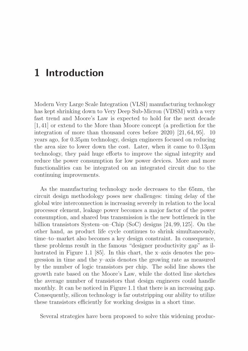
As the manufacturing technology node decreases to the 65nm, thecircuit design methodology poses new challenges: timing delay of theglobal wire interconnection is increasing severely in relation to the localprocessor element, leakage power becomes a major factor of the powerconsumption, and shared bus transmission is the new bottleneck in thebillion transistors System–on–Chip (SoC) designs [24, 99, 125]. On theother hand, as product life cycle continues to shrink simultaneously,time–to–market also becomes a key design constraint. In consequence,these problems result in the famous “designer productivity gap” as il-lustrated in Figure 1.1 [85]. In this chart, the x–axis denotes the pro-gression in time and the y–axis denotes the growing rate as measuredby the number of logic transistors per chip. The solid line shows thegrowth rate based on the Moore’s Law, while the dotted line sketchesthe average number of transistors that design engineers could handlemonthly. It can be noticed in Figure 1.1 that there is an increasing gap.Consequently, silicon technology is far outstripping our ability to utilizethese transistors efficiently for working designs in a short time.
Several strategies have been proposed to solve this widening produc-

2 Introduction 1
Design Complix
ity by M
oore’s L
aw 50%
Designer Productivity 20%~25%
Des
igne
r P
rodu
ctiv
ity
Gap
Time
Gro
wth
Rat
e
Figure 1.1: Designer productivity gap (modified from SEMATECH)
tivity gap. One of the most efficient solutions is using parallel comput-ing, which has received great attention. It has been introduced in manystate-of-the-art applications in the past few years (e.g. Six-Core CPU,MPSoC and parallel processor arrays) [104, 120, 121, 132]. In addition,modulized circuit design has developed to very large SoC by utilizingreusable/configurable Intellectual Property (IP) cores as much as pos-sible [17]. Soon traditional bus transmission architecture will be unableto satisfy the need for more than thousand cores on a single silicon die.Hence, a better network switching method is desired.
These challenges motivate us to analyze their impact on parallel iter-ative algorithms. We try to present a generalized VLSI design conceptthat considers the significant impact on power, performance, cost, re-liability, and time–to–market. To implement an iterative algorithm ona multiprocessor array, there is a tradeoff between the complexity ofan iteration step (assuming that the convergence of the algorithm isretained) and the number of required iteration steps. For example,suppose we have a hardware platform with multiple processors whichrequires an iteration step of the iterative algorithm to be executed Ktimes in order to obtain the convergence. The iteration step is exe-cuted in parallel on the platform. We want to simplify the processorsin order to improve the logical utilization of the platform as shown inFigure 1.2. This simplification will usually cause an increased numberof iterations for convergence. The number of required iterations willincrease from K to K + L. That means the number of data transfer in

1 Introduction 3
Hareware Platform
L KHareware Platform
Simplified
K
Figure 1.2: Iterative algorithm design concept
the interconnections also increases due to the behavior of the iterativealgorithm. Therefore, as long as the convergence properties are guaran-teed, it is possible to adjust the architecture which is normally resultingin an increased number of iteration steps. This reduces the complex-ity with regard to the implementation significantly. However, it is noteasy to find a superior solution to balance the design criteria, especiallyfor the performance/complexity of the hardware, the load/throughputof interconnects and the overall energy/power consumption. An exam-ple of this in the SoC design is the area and the timing optimization.Area is a metric that is aggressively optimized to achieve low chip cost.In contrast, timing closure is achieved when a particular target clockfrequency is met (further timing optimization is not necessary). Opti-mization of one metric can be traded off for the optimization of otherone. Obviously, it is extremely difficult to optimize all metrics at thesame time.
As we will emphasize throughout this thesis, a design engineer mustthink carefully which strategy should be selected for the hardware im-plementation of iterative algorithms. However, a proper decision be-comes more and more difficult as VLSI technology is evolving. Thisproblem motivates us to study the design issues. Four different itera-tive algorithms have been selected, which cover a wide area of currentsignal processing tasks. All of them are implemented and realized inorder to discuss the relationship between circuit design issues and thealgorithmic complexity. The chosen algorithms are:
CORDIC processor A COordinate Rotation DIgital Computer (CORDIC)

4 Introduction 1
can perform a lot of mathematical computations to acceleratemany digital functions and signal processing applications in hard-ware, including linear and orthogonal transformations by requir-ing only shift and add operations. Since the CORDIC is also animportant iterative algorithm, a brief introduction to the genericdefinition and the hardware implementation issues will be givenfirst. It is a simple, but very flexible arithmetical unit. Very sim-ple modifications to the controller lead to linear and orthogonaloperating modes, capable of calculating vector rotations, angleestimations or even multiplications/divisions. Various conditionsconcerning the circuit design issues will be described and com-pared, particularly on the architecture level. We elaborate theway of implementing a CORDIC rotation with reasonable com-putational complexity by trading off the throughput [6, 83].
Discrete Cosine Integer Transform (DCIT) VLSI implementation ofboth forward and inverse CORDIC based Quantized DCIT (QD-CIT) is presented. This configurable architecture not only per-forms multiplierless 8×8 Quantized DCT (QDCT) and 4×4/8×8integer transforms but also contains configurable modules suchthat it can adjust the number of CORDIC rotations for arbi-trary accuracy. Therefore, the presented architecture reduces thenumber of iterations when the target resolution is small (QCIF/-CIF). On the contrary, it will apply more iterations when thetarget resolution is large (Full-HD/Ultra-HD). Moreover, it stillretains an acceptable transformation quality compared to the de-fault methods in terms of PSNR. This leads to a high-accuracyhigh throughput implementation [106,107,112,113].
Parallel Jacobi EVD method Parallel Jacobi method for EigenvalueDecomposition (EVD) is chosen as an example to explain the de-sign concepts concerning tradeoff between the complexity and theiteration (see Figure 1.2). Here, it is chosen since its convergenceproperty is very robust. Simplifying the hardware architecture ispaid by an increased number of rotations due to the behavior ofJacobi’s algorithm. Nevertheless, the computational complexity isactually decreased, which also results in lower energy consumptionper EVD operation [46,109]. The implementation results demon-strate that using the simplified architecture is beneficial concern-ing the design criteria since it yields smaller area overhead, faster

1 Introduction 5
overall computation time and less energy consumption.
Sparse Matrix-Vector Multiplication based on NoC Future integra-tion of more than thousands IP cores for the very large SoC de-sign will soon challenge the current shared bus transmission sys-tem [133]. In this regard, a Sparse Matrix-Vector Multiplication(SMVM) calculator with the chip-internal network is presented asa novel solution for parallel matrix computation to further acceler-ate many iterative solvers in hardware, such as solving systems oflinear equations, Finite Element Method (FEM) and so on [110].This methodology is called Network–on–Chip (NoC). Using NoCarchitecture allows the parallel processors to deal with irregularstructure of the sparse matrices and achieve a high performancein FPGA by trading off the area overhead, especially when thedata transfers are unstable.
In this thesis, our major concern is to explore several VLSI design con-cepts for iterative algorithms. Contrary to conventional circuit designs,usually reducing the logical utilization and increasing the performance,we will further look into parallel computing, configurable architectureand packet–switched network. The goal is not to optimize one or severalcriteria as much as possible, but trying to expose the complete tradeoffcurves and to have a global view on how large the range is for real-lifeapplications. The major contributions of this thesis are:
1. The description of different circuit design challenges is introducedbriefly, especially when the technology node is very small. Thisleads us further to discuss the design impact on iterative algo-rithms from the algorithmic and the architectural point of views.
2. The investigation of VLSI design concepts is presented for futurecircuit design in nanoscale for four selected iterative applications:CORDIC processor for signal processing, configurable transfor-mations for video compression, parallel EVD for communicationand parallel SMVM for solving systems of linear equations. Eachapplication has its own unique design criteria requiring design en-gineers to think carefully. They require investigating the tradeoffsbetween throughput and power consumption, computational com-plexity and transformation accuracy, the number of inner/outer

6 Introduction 1
iterations and energy consumption, data structure and networktopology. These tradeoffs are further elaborated to obtain a bal-anced solution for each application.
3. The circuit implementations of both forward and inverse QD-CIT transformations based on the CORDIC algorithm are pre-sented. The CORDIC based FQDCIT requires only 120 addersand 40 barrel shifters to perform the multiplierless 8×8 FQDCTand 4×4/8×8 forward quantized integer transform by sharing thehardware resources. Hence it can support different video Codecs,such as JPEG, MPEG–4, H.264 or SVC. Furthermore, for a TSMC0.18µm circuit implementation, it can achieve small chip area andhigh throughput for future UHD resolution. On the other hand,the inverse architecture requires only 124 adders and 40 barrelshifters to perform the multiplierless 8×8 IQDCT and quantized4×4/8×8 inverse integer transform. Meanwhile, the ability toadjust CORDIC iteration steps can be used to support differentvideo resolutions.
4. A configurable Jacobi EVD array has been elaborated with bothFull CORDIC (exact rotation, executing W CORDIC iterations,where W is the word length) and µ–CORDIC (approximate ro-tation, executing only one CORDIC iteration) in order to furtherstudy the tradeoff between the performance/complexity of pro-cessors and the load/throughput of interconnects. Moreover, uti-lizing a preconditioned E index method not only reduces morethan 35% computational overhead for the Full CORDIC and 10%for the µ–CORDIC in average, but also omits the floating pointnumber comparators. For a TSMC 45nm circuit implementation,a detailed comparison between area, timing delay and power/en-ergy consumption is done.
5. A solution for sparse matrix computation based on the NoC con-cept is presented. Parallel SMVM computations have been testedin the Xilinx Virtex–6 FPGA. The advantages of introducing theNoC structure into SMVM computation are given by high resourceutilization, flexibility and the ability to communicate among het-erogeneous systems. This configurable solution can be configuredas a larger p×p array as long as there are enough hardware re-sources (p = 2, 4, 8, . . . , 2k, k ∈ N). Moreover, the NoC structure

1 Introduction 7
can guarantee that arbitrary sparsity structures of the matrix canbe handled without interfering the performance by the sparsity ofthe matrix.
This thesis is organized as follows: Chapter 2 gives a brief intro-duction to recent VLSI design trends, on the parallel implementationissues, and the low power design methodology. Then, in Chapter 3, theCORDIC algorithm is introduced and it is shown how it is derived andimplemented. Two typical iterative algorithms based on the CORIDCarchitecture, Discrete Cosine and Integer Transform and parallel JacobiEVD, will be presented and tested in Chapter 4 and Chapter 5 respec-tively. After that, in Chapter 6, SMVM based NoC is presented andpreliminary implementation results are given. Finally, conclusions aregiven in Chapter 7.

8 Introduction 1

2 Introduction to VLSI Design
In this chapter, a brief introduction to the future trend of VLSI designand its circuit design problems will be addressed. Moore’s Law is ex-pected to hold for at least 10 more years. Meanwhile, digital multimediadevices will keep driving the demand for very complex SoC systems. Asingle chip can contain more than billion transistors to support variousfunctionalities. Therefore, before looking into the design issues of iter-ative algorithms, it is very important to review today’s nanoscale VLSItechnology in Section 2.1. The reason how Moore’s Law will continueto influence the circuit design trend will be explained in Section 2.2.Several strategies for obtaining the timing convergence and reducingthe power optimization from a higher design level to the lower level willbe described from Section 2.3 to Section 2.5. The power consumptionof CMOS circuit and the corresponding solutions will be introduced inSection 2.6. At the end, our motivation on VLSI design concepts foriterative algorithms will be clarified in Section 2.7.
2.1 Modern Digital Circuit Design
Silicon technology is now at the stage where it is feasible to incorporatenumerous transistors on a single square centimeter of silicon such thatIntel predicts the availability of 100 billion transistors on a 300mm2 diein 2015 [17]. At this moment, multi-core SoC design emerged because itallowed design engineers to integrate few cores together for simple par-allel computing. This permits to build as a complete SoC for supportingextremely complex functions, which would previously be implementedas a collection of individual chips on a PCB board. Now, since thenano-technology allows the integration of an ever-increasing numberof macro-cells on a single silicon die, parallel multiprocessor platformshave received great attention and have been realized into several state-

10 Introduction to VLSI Design 2
of-the-art applications (e.g. Six–Core, MPSoC and parallel processorarray) [8, 17, 132].
Besides the issue of parallelism, the ability to integrate all parts ofapplications on the same piece of silicon is also beneficial for lowerpower, greater reliability and reduced cost of manufacturing for con-sumer electronic devices. Consequently, increased pressure has beenput on design engineers to meet a much shorter time–to–market, nowmeasured in months rather than years. Particularly, with the new in-dustry standards such as H.264, WCDMA, and WiMAX, which keepdriving the growth of High–Definition TV (HDTV) and smart phone.However, the decreasing development period for a new Application-Specific Integrated Circuit (ASIC) not only results in a very high Non-recurring Engineering (NRE) cost, but also makes it hard to succeedthe goal of time–to–market. Therefore, another popular solution FieldProgrammable Gate Array (FPGA) plays an important role for fittingthe gap between cost and flexibility.
FPGA is an integrated circuit, which is designed to be configuredafter manufacturing. The FPGA configuration is generally specified us-ing a Hardware Description Language (HDL), similar to that used foran ASIC design. Hence, FPGAs can be used to implement any logicalfunction that an ASIC can do. In this way, the capability to updatethe functionality, partial reconfiguration of the design and the low NREcosts offer advantages to many applications [134]. However, the manu-facturing cost per FPGA still makes it unsuitable for many consumerstandard devices. For example, the price of an FPGA die which canbe configured as a video decoder with MPEG–4 decoding functionalitywill be much higher than a dedicated ASIC. Therefore, the choice be-tween the FPGA and the ASIC design is simple the question if eitherthe size of market is large enough to afford ASIC development costs orthe devices need the reconfiguration for supporting new functionalitiesafter shipping.

2.2 Moore’s Law 11
Figure 2.1: Moore’s Law: Plot of x86 CPU transistor counts from 1970 until 2010
2.2 Moore’s Law
In 1965 Gordon E. Moore has predicted a long-term trend of computinghardware, in which the number of transistors that can be placed on anintegrated circuit will double approximately every two years [80]. Notethat it is often incorrectly cited as a doubling of transistors every 18months. The actual average period is about 20 months. Historically,Moore’s Law has precisely described a driving force of technological andsocial change with respect to cost, functionality and performance in thelate 20th and early 21st centuries. For example, if we consider the CPUtransistor counts from 1970 until 2010 in Figure 2.1, it results in a con-stant line corresponding to exponential growth due to the logarithmicscale.
At the beginning, the first x86 Intel 4004 contained only thousandtransistors; 10 years ago, the transistor counts of an Intel Pentium in-creased very fast to a million transistors. Until now a single Quad-Core/Six-Core CPU can integrate more than a billion transistors. InAppendix A, Table A.1 shows more detailed information for each x86

12 Introduction to VLSI Design 2
CPU model. In the future, Moore’s Law will continue until 2020 [41,90]or maybe even further. After that, soon CMOS technology will meetits physical limitation when the node size is smaller than 10nm. Nowmany scientists are trying to replace the current silicon based MOS-FET by a novel carbon based Carbon Nanotube Field Effect Transistor(CNFET) or spintronics in order to shrink the node size into the atomlevel [7, 61, 86]. If it comes true, the computer will usher in a new era“Beyond CMOS” (also known as “More Moore”). Unfortunately, itseems that this is probably not going to happen so easily in the next 10years. On the other hand, other groups came out with another poten-tial way to keep Moore’s Law alive by using a Three-Dimensional IC(3D-IC) concept to increase the density of transistors [66,91]. As far aswe can see the Through-Silicon Via (TSV) technology for 3D-IC will befeasible before 2012.
More and more evidences point out that the trend of Moore’s Lawbecomes slow, especially the 2009 executive summary of InternationalTechnology Roadmap for Semiconductors (ITRS) provides a taxonomyof scaling in the traditional, “More than Moore” sense. Figure 2.2 showsthree possible trends. They envision future integrated circuit systemwill perform diverse functions such as high-accuracy sensing of real-timesignals, energy harvesting, and on-chip chemical/biological sensors in aSystem-in-Package (SiP) or a System-of-Package (SoP) design [64, 95].In this way, the incorporation of functionalities into devices will notnecessarily scale according to Moore’s Law but provide additional valueto the end customer in different ways. The More than Moore approachwill allow for the non-digital functionalities (e.q. RF communication,power control, passive components, sensors, actuators) to migrate fromthe system board-level into particular SiP/SoP potential solutions [119].So far, we still could not tell which solution will dominate the futuredesign trend, especially there are many design issues require engineersfurther discuss.
2.3 Circuit Design Issues: Modular Design
Recently, the growing complexity of multi–core architectures will soonrequire highly scalable communication infrastructure. Today most of

2.3 Circuit Design Issues: Modular Design 13
130nm
90nm
65nm
45nm
32nm
22nm
Analog/RF BiochipsPassives Power Sensors
Very large SoCDigital content
Information Processing
New Standards
SiP/SoP design
Interacting with people and enviroment
Non−digital content
Beyond CMOS
Moo
re’s
Law
More than Moore
Combing SoC and SiP/SoP, Many−Core system
3D IC
Figure 2.2: IC scaling roadmap for More than Moore (modified figure from 2009International Technology Roadmap for Semiconductors Executive Summary) [58]
the current communication architectures in multi-core SoC are stillbased on dedicated wiring. With shirking process technology, logiccomponents such as gates have also decreased in size. However, thetraditional wiring lengths do not shrink accordingly, resulting in rela-tively longer communication path lengths between logic components.For instance, when the technology node is 65nm, the metal–layer wiredelay is 10 times larger than the gate node delay as shown in Figure 2.3.Moreover, the data synchronization issue with a single clock source hasalso become a critical problem for circuit synthesis [14,51]. That meansthe timing closure issue on the large SoC design is difficult to be solved.
In the meantime, design resource reuse concerns all additional activ-ities that have to be performed to generate an easy–to–use and flexibleIP module. This is based on a hierarchical approach, which proceeds bypartitioning a system into many small modules and requires compati-bility and consistency. Proper system partitioning allows independencebetween the design of different modules. The decomposition is gener-ally guided by structuring rules aimed at hiding local design decisions insuch a way that only the interface of each module is visible. This kindof methodology is also called “a modular design”. The overall modularapproach can optimize the insertion of reusable IP component within

14 Introduction to VLSI Design 2
Figure 2.3: Relative delays of interconnection wire and gate in nanoscale level (regen-erated figure from International Technology Roadmap for Semiconductors 2003) [57]
the circuit design.
As a result, ITRS has predicted for the next 20 years that a singleSoC design will integrate more than one thousand IP components. Theyassumed the future die area will keep in a constant size and the numberof cores will increase by a factor of 1.4 per year. Each processor core’soperational frequency and its computational architecture will be bothimproved by a factor of 1.05 per year simultaneously. This means thatthe IP core performance will increase by a factor of 1.1025 per year.Figure 2.4 predicts a roughly 1000 times increase in a multi-core SoCsystem, which is the product number of IP cores and the frequency/per-formance. Therefore, the system performance with about 80-cores willincrease about 20 times compared to an 8-cores implementation in 45nmtechnology in 2009. Note that these two anticipations are based on cur-rent 8-cores for general PC workstations and 2-core for mobile handhelddevices.
In order to satisfy the needs for the very huge modular design (i.e.more than thousand IP cores), the flexible reusable interface and thenanoscale global wire delay problem, Network–on–Chip (NoC) was pre-

2.3 Circuit Design Issues: Modular Design 15
Figure 2.4: The prediction of future multi-core SoC performance (regenerated figurefrom 2009 International Technology Roadmap for Semiconductors System Drivers) [59]
sented as a new SoC paradigm to replace the traditional bus based on-chip interconnections by packet–switched network architecture [14,121,133]. It can yield reduced chip size and cost with higher interconnec-tion efficiency. The components of an on-chip network (e.g. switchingfabric, link circuitry, buffer and control logic) and the module inter-faces, which are designed to be compatible with both heterogeneous IPcores and homogeneous Processing Elements (PEs), are interoperableand reusable.
The NoC can be used to structure the top-level wires on a chip andfacilitate the implementation into a modular design. As shown in Fig-ure 2.5, a typical multi-core system based on a mesh style networkconsists of a regular n×n array of tiles. Each tile could be a general-purpose processor, a DSP, a customized IP core or a subsystem. Thenetwork topology can be mesh, tours, ring, tree, irregular or hybridstyle. A Network Interface (NI) is embedded within each tile for con-necting itself with its neighboring tiles. The communication can beachieved by routing packets in a packet–switched network. This net-
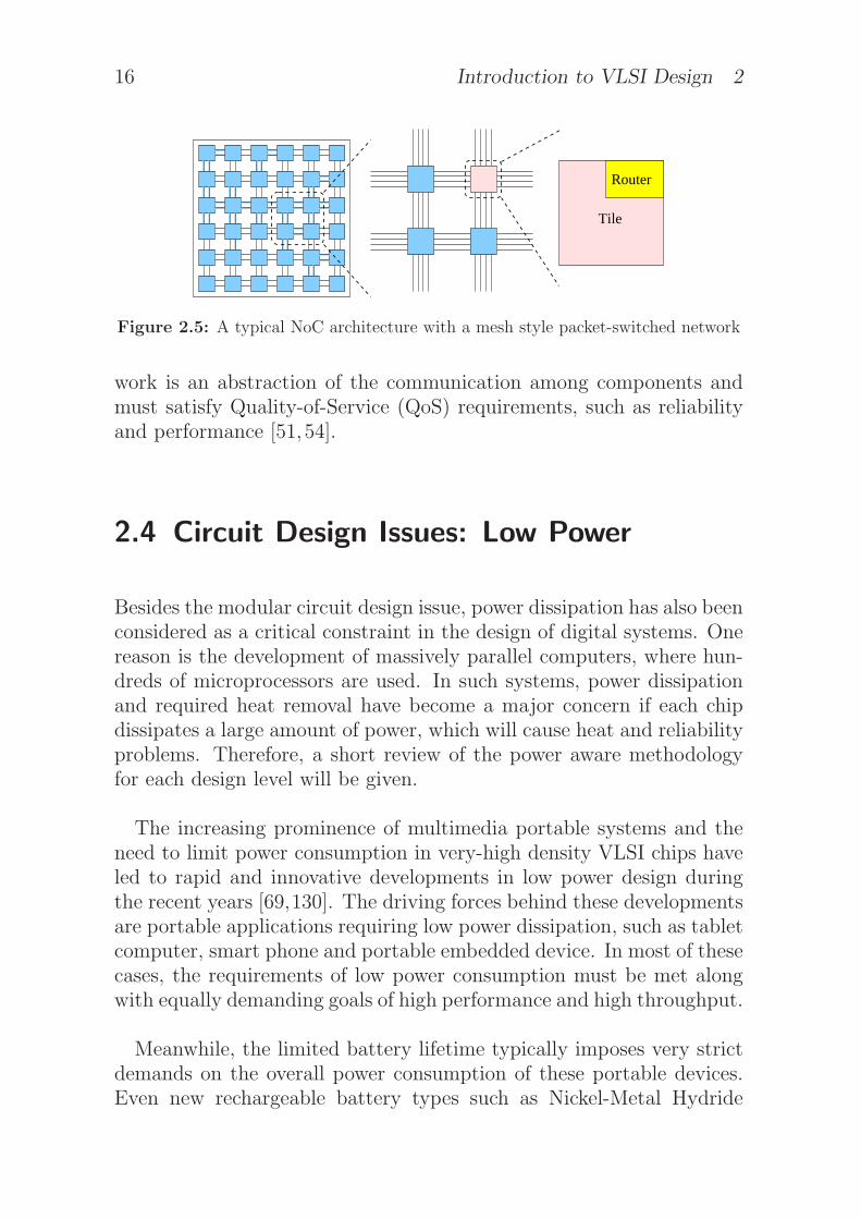
16 Introduction to VLSI Design 2
Router
Tile
Figure 2.5: A typical NoC architecture with a mesh style packet-switched network
work is an abstraction of the communication among components andmust satisfy Quality-of-Service (QoS) requirements, such as reliabilityand performance [51, 54].
2.4 Circuit Design Issues: Low Power
Besides the modular circuit design issue, power dissipation has also beenconsidered as a critical constraint in the design of digital systems. Onereason is the development of massively parallel computers, where hun-dreds of microprocessors are used. In such systems, power dissipationand required heat removal have become a major concern if each chipdissipates a large amount of power, which will cause heat and reliabilityproblems. Therefore, a short review of the power aware methodologyfor each design level will be given.
The increasing prominence of multimedia portable systems and theneed to limit power consumption in very-high density VLSI chips haveled to rapid and innovative developments in low power design duringthe recent years [69,130]. The driving forces behind these developmentsare portable applications requiring low power dissipation, such as tabletcomputer, smart phone and portable embedded device. In most of thesecases, the requirements of low power consumption must be met alongwith equally demanding goals of high performance and high throughput.
Meanwhile, the limited battery lifetime typically imposes very strictdemands on the overall power consumption of these portable devices.Even new rechargeable battery types such as Nickel-Metal Hydride

2.5 Circuit Design Issues: Synthesis for Power Efficiency 17
(NiMH) have been developed with high energy capacity. So far, theenergy density offered by the NiMH battery technology is about 2300-2700 mAh per AA size battery. It is still low in view of the expandingapplications of portable devices. Unfortunately, revolutionary increaseof the energy capacity is not expected in the near future. Therefore,low power and energy efficient computing has emerged as a very activeand rapidly developing field of integrated circuit design.
2.5 Circuit Design Issues: Synthesis forPower Efficiency
In order to meet not only functionality, performance, cost-efficiency butalso power-efficiency, automatic synthesis tools for IC design have be-come indispensable. The recent trend has considered power dissipationat all phases of the design levels. As we can see in Figure 2.6, largeimprovements in power dissipation are possible at the higher levels ofdesign abstraction. The opportunities for reducing power consumptionare higher if we start the design space from the system design level orthe behavioral level. However, with the increasing power dissipation ofVLSI, all possible power optimization techniques are used to minimizepower dissipation at all levels.
• System level - For the first stage, the system architectural andtopological choices are made, together with the boundary betweenhardware and software. This design phase is referred as hardware& software co-design. Obviously, at this stage, the design engineerhas a very abstract view of the system. The most abstract repre-sentation of a system is the function it performs. A proper choicebetween the efficient algorithm and energy budget for perform-ing the function (whether implemented in hardware or software)strongly affects system performance and power dissipation [13,53].
• Behavioral level - After determining the implementation of thefunction by hardware or software, this stage targets on the opti-mization of hardware resources and the optimization of the aver-age number of clock cycles per task required to perform a given

18 Introduction to VLSI Design 2
Figure 2.6: Power reduction at each design level [88]
set of modularized tasks [96]. Moreover, refined task arrangementfor parallelism choosing an appropriate topology of the intercon-nection network also play important roles at this level.
• RTL level - RTL level design is the most common abstractionlevel for the manual design concept. The description is thentransformed into logic gate implementation. At this level, all syn-chronous registers, latches and combinational logics between thesequential elements are described in a HDL program such as Ver-ilog or VHDL. Moreover, the right choice of clock optimizationstrategy and pipelining will strongly affect the power consump-tion [67, 138].
• Logic level - The goal of this level is to generate a structural viewof a logic-level model. Logic synthesis is the manipulation of logicspecifications to create logic models as interconnection of logicprimitives. Thus logic synthesis determines the micro structure ofa circuit at gate-level. The task of transforming a logic model intoan interconnection instance (netlist) of library cells (i.e. the back–

2.6 Circuit Design Issues: Source of Power Dissipation 19
end logic synthesis tools), is often referred to as a library bindingor a technology mapping [78]. At logic level, low power synthesisfor a large SoC chip can be further reduced in average 10%–20% byapplying these methodologies: Multi–Voltage, Multi–ThresholdCMOS (MTCMOS) or Power Gating [20, 67].
• Physical level - In the last stage, the circuit representation is con-verted into a layout of the chip. Layout is created by convertingeach logic component (cells, macros, gates or transistors) into ageometric representation with specific shapes in multiple layers,which performs the intended logic function of the correspondinginstance. Connections between different instances are also ex-pressed as geometric patterns, typically lines, in multiple layers.Various power optimization techniques such as partitioning, fineplacement, MEMS based power switch, transistor resizing, dy-namic voltage scaling are employed [89, 92]. However, only 5%–10% power reductions could be obtained at this level.
2.6 Circuit Design Issues: Source of PowerDissipation
Power consumption in a CMOS technology can be described by a simpleequation that summarizes the three most important contributors to itsfinal value [15, 87].
PTotal = PDynamic + PShort + PLeakage. (2.1)
These three components are dynamic power dissipation (PDynamic),short circuit power dissipation (PShort) and leakage power dissipation(PLeakage). PLeakage considers the static power consumption when thecircuit is in static mode. This static power consumption is important forbattery life in standby mode because the power is consumed wheneverthe device is powered up. PShort and PDynamic are both considered asdynamic power which is important for battery life when operating as itrepresents the power consumed when processing data.

20 Introduction to VLSI Design 2
VDD
VSSVSS
IN
CLIN
IP
ISC
Figure 2.7: A simple CMOS inverter
2.6.1 Dynamic Power Dissipation
For the dynamic power consumption, Figure 2.7 illustrates the currentsof a simple CMOS inverter. Assume that a pulse of data is fed intothe transistor charging up and charging down the device. Power is con-sumed when the gate drives its output to a new value. It is dependenton the resistance values of the pmos transistor and the nmos transistorin the inverter. Hence, the charging and discharging of the capacitorsresult in the dynamic power consumption [131,134]:
PDynamic = CL(VDD − VSS)2fα. (2.2)
When the ground voltage VSS is assumed to be 0. It reduces to abetter-known expression:
PDynamic = CLV2DDfα, (2.3)
where CL is the loading capacitance at the output of the inverter, VDD
denotes the supply voltage and f is the clock frequency. These threeparameters are primarily determined by the fabrication technology andcircuit layout. α is the switching activity level and is dependent onthe target applications (referred as the transition density), which canbe determined by evaluating the logic function and the statistical prop-erties of the input vectors. Table 2.1 lists the probability for the dif-ferent kind of input singles. Obviously, Equation 2.2 shows that thedynamic power dissipation is proportional to the average switching ac-tivity, which means that it is influenced by the target application. In a

2.6 Circuit Design Issues: Source of Power Dissipation 21
Signal Activity (α)
Clock 0.5Random data signal 0.5Simple logic circuits driven by random data 0.4-0.5Finite state machines 0.08-0.18Video signals 0.1(MSB)-0.5(LSB)Conclusion 0.05-0.5
Table 2.1: Typical switching activity levels [5]
typical case, dynamic power dissipation is usually the dominant fractionof total power dissipation (50%–80%).
2.6.2 Short Circuit Power Dissipation
Short-circuit currents occur when the rise/fall time at the input of agate is larger than the output rise/fall time, causing imbalance andmeaning that the supply voltage VDD is short-circuited for a very shortspace of time. This will particularly happen when the transistor isdriving a heavy capacity load. Fortunately, the short circuit current ismanageable and can easily be avoided in a good design or synthesizedby a well condition back–end logic synthesis tool. Therefore, the PShort
power dissipation is usually a small fraction (less than 1%) of the totalpower dissipation in CMOS technology.
2.6.3 Static Leakage Power Dissipation
The scaling of VLSI technology has provided the inspiration for manyproduct evolutions as it gives a scaling of the transistor dimensions, asillustrated in Figure 2.8, where the length and the width are scaled by afactor of k. That means the new dimensions are given by L = L
k, L = L
k
and Tox = Tox
k. This will result in a transistor area reduction up to 1
k2
and also increase the transistor speed. Moreover, an expected decreasein transistor power dissipation as known as currents should be equallyreduced.

22 Introduction to VLSI Design 2
���������������
���������������
�������������������������������������������������
�������������������������������������������������
Oxide
W
L
n+ n+
Gate
DrainSource
IRev IRev
Tox
P-well
ISub
IGIDL
IGate
Figure 2.8: There are four components of leakage sources in NMOS: Subthresholdleakage (ISub), Gate-oxide leakage (IGate), Reverse biased junction leakage (IRev) andGate Induced Drain Leakage (IGIDL)
However, when the node size is smaller than 65nm, a formerly ignor-able gate leakage current (IGate) keeps raising explosively when the Tox isreduced to Tox
kbecause the depth of gate oxide between first metal layer
and P-well is too short. Fortunately, this problem had already beensolved by using high-k dielectric materials to replace the conventionalsilicon based dioxide to improve the gate dielectric. This allows similardevice performance, but with a thicker gate insulator, thus avoidingthis leakage current. In a similar situation, the Reverse biased Junction(IRev) leakage and the Gate Induced Drain Leakage (IGIDL) can both besuppressed efficiently in the manufacturing process with new materials.
On the other hand, in order to avoid excessively high electric fieldsin the scaled structure, the input voltage VDD is required to be scaled.This forces a scaling in the threshold voltage VT , too, otherwise thetransistor will not turn off properly. In the past, subthreshold conduc-tion was generally viewed as a parasitic leakage in a state that wouldideally have no current. However, now the reduction in VT will resultin an increase of subthreshold drain current (ISub) with a direction fromthe drain to the source in a MOSFET. When the transistor is in thesubthreshold region or weak-inversion region, it can be defined as [67]:
ISub = (µCoxV2th
W
L)e
VGS−VTnVth , (2.4)
where W and L are the dimension of the transistor, µ is a carrier mobil-

2.7 Design Consideration for Iterative Algorithms 23
ity, Cox is the gate capacitance, Vth is the thermal voltage kT/q (25mVat a room temperature), VGS is the gate-source voltage, n is a num-ber of the device manufacturing process with a range from 1.0 to 2.5.These parameters are considered as constant coefficients for subthresh-old leakage problem. Therefore, the major coefficient is the exponentof VGS − VT . Once we decrease the VDD and VT during shrinking thesize of the transistor nodes simultaneous, this results in an exponentialincrease of the subthreshold leakage power dissipation. In early VLSIcircuits, ISub leakage was a small fraction (far less than 5%) of the totalpower dissipation. However, this expected decrease in power consump-tion now becomes a nightmare when the node size is smaller than 65nm(could be more than 50%). So far, the most efficient way to reduce theISub leakage power is power gating, when the entire macro is turned off.
2.7 Design Consideration for IterativeAlgorithms
With aforementioned design issues, we have to consider the relationshipbetween iterative algorithms and design criteria for circuit implemen-tation. First of all, as mentioned in Section 2.4, we already know thatthe system level stage provides the most opportunities to reduce thepower dissipation. On the other hand, according to the source of powerdissipation in Section 2.6, the major sources of power dissipation aredynamic and leakage power dissipations in CMOS circuit. Therefore,to design a low power iterative architecture that can reduce both dy-namic and static power dissipations significantly at the system level isone of the major topics in this thesis. In the following chapters, a VLSIdesign concept will be clarified by four different iterative algorithm-s/methodologies. These hardware solutions not only balance with thecircuit design criteria (area, timing and power) but also retain the goodquality of results.
Iterative algorithms usually have a common character, more precisecomputation or approximation per iteration step will result in morearea overhead for iterative hardware core. On the one hand, less pre-cise iteration steps will cause slower convergence property. On the otherhand, more precise iteration steps will consume more energy. Here we
24 Introduction to VLSI Design 2
will elaborate two iterative examples, CORDIC based QDCIT trans-formation for video compression and parallel Jacobi method for EVD.They will be handled carefully with a balance between the cost/area,convergency/timing and energy/power.
On–chip network emerges for the next generation SoC and becomesmore and more important. With the need for supporting many mul-timedia standards in a single chip, it has been predicted more thanone thousand processor units will be integrated together in the future.However, current bus methodology is facing a critical challenge of dataswitching for supporting large scale SoC, especially when these proces-sor units are heterogeneous. Moreover, the timing closure will becomeextremely difficult to be obtained. Therefore, the choice between theordinary bus-based system and switching based network is a criticaldesign issue especially when the data transfers are irregular. Later, wewill show how to utilize this switching feature for Sparse Matrix-VectorMultiplication (SMVM) when solving systems of linear equations iter-atively.
2.8 Summary
In this chapter, a brief introduction to the concerns of today’s nanoscaleVLSI design concepts was given. It was shown that dealing with thepower dissipation problem became one of the important tasks concern-ing an ASIC development. It will cause very huge efforts for both verifi-cation and implementation when the power sources are not guaranteed.Therefore, design engineers must carefully think about the relationshipbetween the design criteria (area, timing and power/energy) and theproper way how to realize iterative algorithms in hardware. In nextchapter, we will start to discuss the relationship between these im-portant design issues by a well–known iterative algorithm, “CORDIC”algorithm, which can be used to accelerate many digital functions andapplications in signal processing.

3 CORDIC Algorithm
COordinate Rotation DIgital Computer (CORDIC) is a typical itera-tive algorithm which is used to accelerate many digital functions andapplications in signal processing. In this chapter, a brief introductionto the generic definition of the CORDIC algorithm with orthogonal ro-tation mode will be given first in Section 3.1. Then the extension ofCORDIC to linear and hyperbolic modes will be further explained inSection 3.2. In Section 3.3, three different dependence flow graphs forthe CORDIC hardware implementation will be described and comparedin Section 3.4.
3.1 Generic CORDIC Algorithm
Digital Signal Processing (DSP) algorithms exhibit an increasing needfor the efficient implementation of complex arithmetic operations. Thecomputation of trigonometric functions, coordinate transformations orrotations of complex valued phases are almost naturally involved withmodern DSP algorithms. Popular application examples are algorithmsused in digital communication technology and in adaptive signal pro-cessing. There are many applications using the CORDIC algorithm,such as solving systems of linear equations [2,4,55,60], computation ofeigenvalues and singular values [30,38,102], Discrete Wavelet Transform(DWT) [28,103], Discrete Cosine Transform (DCT) [75,112] and digitalfilters [31, 32, 115]. The CORDIC algorithm offers the opportunity tocalculate all the desired functions and applications in a rather simpleand elegant way in circuit design [6].
The CORDIC algorithm was first presented by Jack Volder in 1959[122] for the computation of trigonometric function, multiplication, divi-sion, data type conversion, and later generalized to hyperbolic function
26 CORDIC Algorithm 3
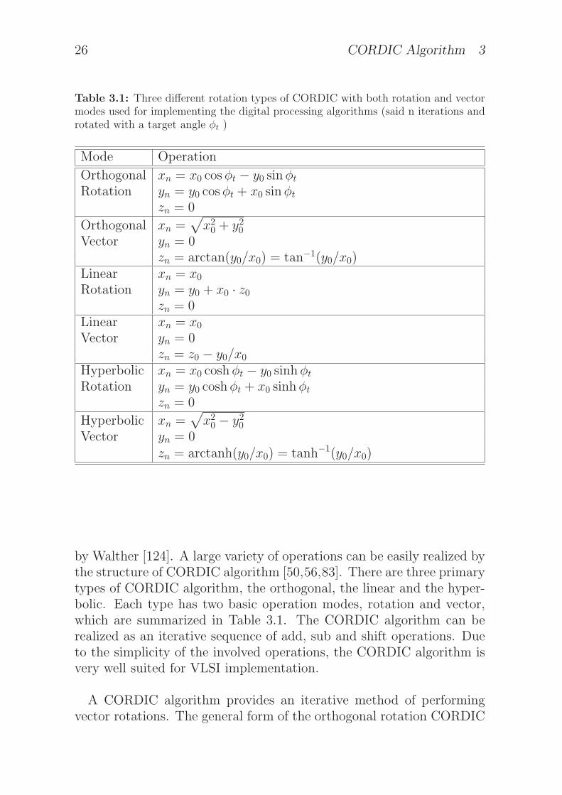
Table 3.1: Three different rotation types of CORDIC with both rotation and vectormodes used for implementing the digital processing algorithms (said n iterations androtated with a target angle φt )
Mode Operation
Orthogonal xn = x0 cosφt − y0 sinφt
Rotation yn = y0 cosφt + x0 sinφt
zn = 0
Orthogonal xn =√
x20 + y20Vector yn = 0
zn = arctan(y0/x0) = tan−1(y0/x0)Linear xn = x0Rotation yn = y0 + x0 · z0
zn = 0Linear xn = x0Vector yn = 0
zn = z0 − y0/x0Hyperbolic xn = x0 coshφt − y0 sinhφt
Rotation yn = y0 coshφt + x0 sinhφt
zn = 0
Hyperbolic xn =√
x20 − y20Vector yn = 0
zn = arctanh(y0/x0) = tanh−1(y0/x0)
by Walther [124]. A large variety of operations can be easily realized bythe structure of CORDIC algorithm [50,56,83]. There are three primarytypes of CORDIC algorithm, the orthogonal, the linear and the hyper-bolic. Each type has two basic operation modes, rotation and vector,which are summarized in Table 3.1. The CORDIC algorithm can berealized as an iterative sequence of add, sub and shift operations. Dueto the simplicity of the involved operations, the CORDIC algorithm isvery well suited for VLSI implementation.
A CORDIC algorithm provides an iterative method of performingvector rotations. The general form of the orthogonal rotation CORDIC

3.1 Generic CORDIC Algorithm 27
mode is defined as:
x′ = x cosφt − y sinφt
y′ = y cosφt + x sinφt,(3.1)
which rotates the input vector < x, y > in the Cartesian coordinatesystem by a rotation angle φt. Then this equation can be rearrangedas:
x′ = cosφt(x− y tanφt)y′ = cosφt(y + x tanφt).
(3.2)
To further simplify it, we can restrict the rotation angle tanφt totanφt = ±2−i, such that the multiply operation by the tangent partis reduced to shift operations. This alters Equation 3.2 to become asequence of arbitrary elementary rotations. Since the decision at eachiteration i is fixed, the cos2−i = cos2i becomes a constant number. Thenew iterative rotation can now be defined as:
xi+1 = Ki(xi − yi · di · 2−i)yi+1 = Ki(yi + xi · di · 2−i)Ki = cos(tan−1 2−i) = 1√
1+2−2i
di = ±1i = 0, 1, 2, 3, . . . n.
(3.3)
Removing the scaling factor Ki from the iterative part yields a sim-ple shift-add algorithm for orthogonal rotation CORDIC. After severaliterations, the product of Ki factors will converge to a constant coef-ficient 0.607252. The exact gain depends on the number of iterations:An =
∏
n
√1 + 2−2i ≈ 1.646762 = 1
Kn. In the mode of orthogonal rota-
tion, the angle accumulator is added to the Equation 3.4.
xi+1 = xi − yi · di · 2−iyi+1 = yi + xi · di · 2−izi+1 = zi − di · tan−1 2−idi = −1 when zi < 0 else + 1.
(3.4)
The angle accumulator is initialized with the input rotation angle.The rotation direction at each iteration i is decided by the magnitudeof the residual angle in the angle accumulator. If the residual angle is

28 CORDIC Algorithm 3
ScalingRotating
< xn, yn >
< xs, ys >
< x0, y0 >
< xn, yn >< x2, y2 >
< x1, y1 >
n times
φt
Figure 3.1: CORDIC rotating and scaling a input vector < x0, y0 > in the orthogonalrotation mode
positive, then the di is set to +1 otherwise -1. After serveral iterations,it will produce the following results:
xn = An(x− y tan z0)yn = An(y + x tan z0)zn = 0.
(3.5)
In Figure 3.1, an example for the generic CORDIC processor rotatingan input vector < x0, y0 > with a target rotation angle φt is shown. TheCORDIC processor rotates it by the desired rotation angle iteratively,said n times (usually n = 32 with the single floating precision). Afterthat, a constant scaling value K = 0.607252 will be applied to therotated vector < xn, yn > in order to scale the rotation results.
Moreover, for the orthogonal vector mode, the CORDIC rotates theinput vector through whatever angle is necessary to align the resultingvector with the x axis. That means the direction di is dependent on thecurrent yi instead of zi. Equation 3.4 can be modified as:
xi+1 = xi − yi · di · 2−iyi+1 = yi + xi · di · 2−izi+1 = zi − di · tan−1 2−idi = −1 when yi ≥ 0 else + 1.
(3.6)

3.1 Generic CORDIC Algorithm 29
Rotating
n times
< xn, yn >
< x0, y0 >
< x1, y1 >
< x2, y2 >φn
Figure 3.2: CORDIC rotating a input vector < x0, y0 > in the orthogonal vectormode
Then:
xn =√
x20 + y20yn = 0zn = z0 − di · tan−1 2−i.
(3.7)
The CORDIC with orthogonal vector mode can obtain the arctan-gent result, φ = arctan(y
x), if the angle accumulator is initialized with
zero (z0 = 0). Since the arctangent result is taken from the angle accu-mulator, the scaling factor An can be ignored and does not affect theresult.
zn = arctan( y0x0
). (3.8)
Figure 3.2 shows an example when a CORDIC processor rotates aninput vector < x0, y0 > to the x axis iteratively. After n iterations, theφn=arctan( y0
x0
), will converge into the zn accumulator. Note that theconstant scaling value K = 0.607252 for correcting the < xn, yn > isnot necessary if we only need the arctangent result.

30 CORDIC Algorithm 3
3.2 Extension to Linear and Hyperbolicfunctions
A simple modification to Equation 3.4 allows the computation of func-tion in the linear coordinate system using the same architecture:
xi+1 = xi − 0 · yi · di · 2−i = xiyi+1 = yi + xi · di · 2−izi+1 = zi − di · 2−i
i = 1, 2, 3, 4, . . . n.
(3.9)
For the linear rotation mode, di = -1 if zi < 0 else +1, the linearrotation CORDIC produces:
xn = x0yn = y0 + x0 · z0zn = 0.
(3.10)
This operation is more and less like a multiplier but requires only theshift and add operations. It is a very efficient approximated solutionfor iterative hardware design [82]. Of course there are more efficientimplementations of MAC like structures and especially multipliers, butif a CORDIC is already available it may be used as such [53]. On theother hand, if we redefine di = -1 if yi ≥ 0 else +1, the linear vectormode results will be converted as:
xn = x0yn = 0zn = z0 − y0
x0
.(3.11)
On the contrary, the linear vector mode now can approximate a divideoperation iteratively, which is very important for DSP system. Notethat the rotations in the linear coordinate system have only a unitygain, so there is no scaling factor for compensation. In Appendix B,two linear CORDIC examples with the rotation mode and the vectormode are described in Figure B.1 and Figure B.2.

3.2 Extension to Linear and Hyperbolic functions 31
The difference between trigonometric function and hyperbolic func-tion is very small, they can share the same CORDIC architecture witha little modification to Equation 3.4. In this case the formulas for thehyperbolic rotation mode are:
xi+1 = xi + yi · di · 2−iyi+1 = yi + xi · di · 2−izi+1 = zi − di · tanh−1 2−i
i = 1, 2, 3, 4, 4, 5, . . . 12, 13, 13, 14, . . . n,
(3.12)
where di = -1 if zi < 0 else +1, then the hyperbolic rotation CORDICwill produce:
xn = An(x+ y tanh z0)yn = An(y + x tanh z0)zn = 0
An =∏
n
√1− 2−2i ≈ 0.80.
(3.13)
Moreover, for the hyperbolic vector mode, di = +1 if yi < 0 else -1,then the hyperbolic vector CORDIC produces:
xn =√
x20 − y20yn = 0zn = z0 + tanh−1 y0
x0
.(3.14)
It should be noticed that the rotations in the hyperbolic coordinatesystem do not converge. It will only converge if we select a particulariteration sequence, i.e. i = 4, 13, 40, . . . , k, 3k + 1, . . . are repeated once[2, 124]. The hyperbolic equivalents of all the functions as the circularcoordinate system can be computed in a similar fashion. In Appendix B,two hyperbolic CORDIC examples for the rotation mode and the vectormode are described in Figure B.3 and Figure B.4. Essentially, these sixdifferent rotation modes can be summarized into an unified formulaas (i.e. orthogonal rotation, orthogonal vector, linear rotation, linear

32 CORDIC Algorithm 3
vector, hyperbolic rotation and hyperbolic vector):
xi+1 = xi −m · yi · di · 2−iyi+1 = yi + xi · di · 2−izi+1 = zi − di · ei
ei =
tan−1 2−i when m = 12−i when m = 0tanh−1 2−i when m = −1
,(3.15)
where ei is the elementary angle of rotation for iteration i in the selectedcoordinate system. For orthogonal mode in the Cartesian coordinatesystem, the ei = tan−1 2−i and the m=1. For linear mode in the linearcoordinate system, the ei = 2−i and the m=0. For hyperbolic mode inthe hyperbolic coordinate system, the ei = tanh−1 2−i and the m=-1.This universal representation, credited to Walther, permits the designof a general purpose CORDIC rotation processor. However, the focusof this thesis will be only on the orthogonal rotation and the orthogonalvector modes.
3.3 CORDIC in Hardware
In this section, three different dependence flow graphs are presented forthe hardware implementation of the CORDIC. Note that we restrictonly to the conventional CORDIC iteration scheme as shown in Equa-tion 3.15. In Figure 3.3, the structure of one stage of the CORDICiteration is presented, which requires a pair of adders for rotation andanother adder for steering the next angle direction (di). All internal vari-ables are buffered in the registers separately until the iteration numberis large enough to obtain convergence. The signs of all three interme-diate variables are fed into a control unit which generates the rotationdirection flags di to steer the add or sub operations and keeps trackingof the rotation angle zi. This folded dependence graph is typical forthe orthogonal rotation mode and has its benefit in small area for VLSIdesign. However, the throughput is very low and requires an extra stor-age (lookup table) to store the rotation angles for following iterations.Moreover, it requires a number of different shifting lengths according

3.3 CORDIC in Hardware 33
add
add
adder or substractor
buffer register
right shift k bit
2x1 multiplexer
Look-Up Table
Reg
Reg
Reg
Reg
add
>>k
>>k
>>k
add
mux
ROM
ROM
di
zout
yout
xoutx0
y0
z0
−mdi
−di
mux
mux
mux
Figure 3.3: Flow graph of a folded CORDIC (recursive) processor
to the chosen shift sequence, additional barrel shifters are required infolded CORDIC architecture.
We can unfold it to improve the throughput and obtain a new flowgraph where n = 32 stages are cascaded together as shown in Fig-ure 3.4. Note that the fixed shift operations are assumed to be hard-wired, hence they do not represent any propagation delay or furtherhardware resources. In this way, the lookup table is not required andeach stage has a specified constant number for steering the next stage’sangle direction.
Besides having a purely combinational implementation, buffers canalso be inserted between successive stages as indicated in Figure 3.5. Inthis way, the throughput of the unfolded CORDIC can be improved byusing a pipelined architecture. Table 3.2 lists the overall comparison foreach flow graph in terms of area, speed and power consumption. It canbe noticed that the folded CORDIC is smaller than the other two flowgraphs but the processing speed is much slower. On the contrary, thepipelined CORDIC achieves higher throughout but requires larger areaoverhead. Therefore, the choice between folded, unfolded and pipelinedsimply becomes a tradeoff problem. Design engineers must further con-sider which solution is best for their system design.

34 CORDIC Algorithm 3
right shift k bit
add
add add
add
adder or substractor >>k
>>0
>>0
>>1
>>1
>>2 >>31
>>31>>2
add
add add addadd
const
x0 xout
yout
zout
const
add
add
const
add
add
const
y0
z0
d0
−md0
d1 d2
−md1 −md2
d31
−md31
Figure 3.4: Flow graph of an unfolded (parallel) CORDIC processor
RE
GR
EG
RE
G
add
add
RE
GR
EG
RE
G
RE
GR
EG
RE
G
right shift k bit REGadder or substractor pipeline buffer
add
add
>>1
>>1
>>2
>>2
>>31
>>31
>>kadd
>>0
>>0
add add
const
d1
−md1
add
add
add
const
d2
−md2
add
xout
yout
zout
add
add
const
d31
−md31
const
x0
y0
z0
d0
−md0
Figure 3.5: Flow graph of an unfolded (parallel) CORDIC processor with pipelining
Table 3.2: Comparison of three different CORDIC dependence flow graphs
Mode Area Speed Power
folded small very slow lowunfold large slow highpipeline very large very fast very high

3.4 Hardware Performance Analysis 35
Table 3.3: Implementation results of three different CORDIC dependence flow graphswith the orthogonal rotation mode in Xilinx Virtex–5 FPGA (xc5vlx110t-1ff1136)
folded unfold pipeline
Slice Regs 502 162 3,204Slice LUTs 477 3,528 3,106Timing 7.340 ns 94.732 ns 5.347 nsFrequency 136.2 MHz 10.6 MHz 187 MHzThroughput (MByte) 34.04 MB 84.8 MB 1496 MBPower Consumption 27.44 mW 14.92 mW 53.38 mWEnergy (per byte) 0.8061 nJ 0.1759 nJ 0.0357 nJ
3.4 Hardware Performance Analysis
In order to further analyze these three different dependence flow graphs,they are directly generated from the Xilinx IP core library and synthe-sized by the Xilinx ISE 11.5 in Virtex–5 FPGA, where Table 3.3 lists thesynthesis results. Note that each generated CORDIC hardcore requires32 iterations and the input/output word length is 32 bits.
First of all, the area size of the folded CORDIC is very small comparedto the others, but the throughput is very low. Although the pipelinedCORDIC can achieve higher throughput, the area overhead is very high(due to cascaded units and pipeline buffers) and the power consump-tion is also high. Second, the timing delay of the unfold CORDIC flowgraph is much larger than the others due to its very long data path forclock tree synthesis. Third, if we further consider the energy consump-tion per byte, the pipelined CORDIC is much more efficient than thefolded CORDIC, because the computation period is shorter. Finally,the FPGA synthesis results show that the pipelined CORDIC archi-tecture can achieve higher throughput and low power but require morelogical utilization resources in FPGA. On the other hand, the foldedCORDIC is small and simple. However, it is very slow and not efficientconcerning the energy consumption.

36 CORDIC Algorithm 3
3.5 Summary
In this chapter, a brief introduction to the fundamental CORDIC algo-rithm with different rotation modes and the corresponding VLSI circuitdesign of three dependence flow graphs was given. The folded CORDICflow graph is smaller than the pipelined CORDIC but the throughputis slow. Furthermore, the energy consumption is also higher. Therefore,the design tradeoff is between the throughput and the energy consump-tion. The choice is dependent on the target application. Although onlythe orthogonal rotation and orthogonal vector modes are used in thisthesis, the presented VLSI design concepts can also be applied to otherCORDIC rotation modes.

4 Discrete Cosine Integer Transform(DCIT)
In this chapter, the integration of DCT and integer transform on a con-figurable IP Core for supporting multi–standard image/video Codecs ispresented. In Section 4.1, a short review on today’s video transforma-tion and quantization will be given first. Section 4.2 briefly introducesthe algorithms of the DCT, Loeffler DCT, CLDCT and the integertransforms. In Section 4.3, a configurable forward and inverse DCITfor supporting the multiple transformations is presented. Later, theframework of the proposed CORDIC based Quantized DCIT architec-ture on a schematic design level will be described in Section 4.4. Theimplementation results are shown in Section 4.5. Section 4.6 summa-rizes this chapter.
4.1 Introduction of DCIT
As the demand for multi-function devices has been growing severelyin recent years, more and more requirements have been posed for SoCdesign, such as low power, high performance, quality awareness andmulti-standard integration. The DCT transformation is a very im-portant video coding component of many modern Image/Video com-pression standards (e.g. JPEG, MPEG–2, MPEG–4, H.263 and soon [26, 94]). In H.264 Codec, which is a joint standard of the ITU-Tvideo compression and the ISO/IEC MPEG-4 Part 10 Advanced VideoCoding (AVC), the DCT part is replaced by an integer transform usinga block size of 4×4 pixels. For adding profiles for High Definition (HD)videos, an integer transform using a block size of 8×8 pixels has beenadded [74]. Recently, the H.264/AVC has been extended to supportScalable Video Coding (SVC) by Joint Video Team of ITU-T VCEG
38 Discrete Cosine Integer Transform (DCIT) 4
and ISO MPEG (JVT) [100,101]. Furthermore, Ultra–HD (UHD) TV,producing a 7,680×4,320 pixel resolution (a.k.a. Super Hi-Vision) andthe next generation High Efficiency Video Coding (HEVC), will soonneed very high throughput performance [25, 79]. Therefore, the multi-function integration of different Codecs with very high throughput is achallenge to design engineers implementing the Codecs for supporting3D/UHD displays.
A low–power and high-quality CORDIC based Loeffler DCT (CLDCT)is presented. It can reduce the computational complexity from 11 muland 29 add operations to 38 add and 16 shift operations [112]. It ob-tains a transformation quality as good as the original Loeffler DCT.Furthermore, 4–point integer transform and 8–point integer transformare integrated in this CLDCT [106], such that a configurable architec-ture for Discrete Cosine and Integer Transform (DCIT) is obtained. Itcan be configured to perform the multiplierless One–Dimensional (1–D) 8–point DCT and the 1–D 4–point/8–point integer transforms inmulti-standard Video Codecs.
In general, the Two–Dimensional (2–D) DCT coefficients are usu-ally followed by a quantization procedure in image/video compressions.Quantization can be uniform or nonuniform. The uniform quantiza-tion method is typically implemented as a division by a quantizationstep size followed by a rounding operation. The nonuniform quantiza-tion method can be implemented in a large lookup table or by utiliz-ing a search algorithm in a code book. Incorporating the quantizationinto the DCT transformation, resulting in Quantized DCT (QDCT),has been considered as an efficient way to improve the computationalcomplexity for video compression. Essentially, only the uniform quan-tization can be incoperated into the DCT transformation due to itsregular structure, which is more efficient for VLSI implementation. Inthe literature, Alen Docef et al. [34] proposed a joint implementationof Chen’s DCT [23] and Quantization (i.e. a conventional QDCT de-sign). Later, Hanli Wang et al. [126] merged the quantization processrepresented by a quantization matrix that has variable quantizationstep sizes into Chen’s DCT. They called it Novel QDCT (NQDCT).However, both QDCT designs require multipliers to perform DCT andQuantization. Even if the multiplier could be replaced by CanonicalSigned Digit (CSD) representation, the QDCT and NQDCT will needmore than 300 add operations, in the worst case.

4.2 DCT algorithms 39
In this chapter, instead of realizing the QDCT architecture with mul-tiplications, CORDIC compensation steps are used to approximate thequantization procedure iteratively. As for CLDCT in [112], the numberof CORDIC compensation iterations is reduced, resulting in a CORDICbased Scaler (CORDIC-Scaler). This CORDIC-Scaler has five stagesand requires 8 adders and 10 shifters to approximate two scaling oper-ations. The combination of two 1–D DCITs, a row-column transposi-tion memory and four CORDIC-Scalers forms a 2–D Forward QDCIT(FQDCIT) which requires 120 adders and 40 shifters. On the otherhand, an extended version of Inverse QDCIT (IQDCIT) has also beenmodified with seven configurable modules which requires 124 addersand 40 shifters. The proposed core can save more than the half numberof adders by using a shared configurable architecture. This CORDICbased IQDCIT can support arbitrary scaling values for quantizationby updating the lookup tables for different Codecs which are basedon scaler dequantizer, such as JPEG, MPEG–4, H.264 or DivX. Af-ter that, different numbers of CORDIC iterations are applied to theInverse DCIT (IDCIT) and different numbers of compensation stepsto the CORDIC-Scaler, respectively, because in most image/video de-coders, the required transformation precision is dependent on the targetresolution. For example, the concept of dynamic Bit-width adaptationby decreasing the bit length of the high frequency coefficients in DCThas also been adopted into our design [84]. Therefore, it will performfewer iterations when the target resolution is small (QCIF/CIF). Onthe contrary, when the target resolution is large (Full-HD/Ultra-HD),more iterations will be applied. Providing arbitrary accuracy for variousresolutions is important for embedding video decoders in any consumerelectronic devices.
4.2 DCT algorithms
4.2.1 The DCT Background
A 2–D DCT can transform an 8× 8 block sample from spatial domainX(i, j) into frequency domain Y (k, l) as follows:

40 Discrete Cosine Integer Transform (DCIT) 4
Y (k, l) = 14C(k)C(l)
7∑
i=0
7∑
j=0
X(i, j) · cos[ (2i+1)kπ16 ] cos[ (2j+1)lπ
16 ]
C(k) =
{ 1√2
if k = 0
1 otherwiseC(l) =
{ 1√2
if l = 0
1 otherwise
k and l = 0, 1, 2, . . . 7.
(4.1)
Since computing the above 2–D DCT by using matrix multiplicationrequires 84 multiplications, a commonly used approach to reduce thecomputational complexity is row-column decomposition. This decom-position performs row-wise 1–D transformation followed by column-wise1-D transformation with intermediate transposition. This approach hastwo advantages. First, the computational complexity is significantly re-duced. Second, the original 1–D DCT can be easily replaced by differentDCT algorithms. A 1–D 8–point DCT can transform 8 samples X(i)into the frequency domain Y (k) as follows:
Y (k) = 12C(k)
7∑
i=0
X(i) cos[ (2i+1)kπ16 ]
C(k) =
{ 1√2
if k = 0
1 otherwise
k = 0, 1, 2, . . . 7.
(4.2)
4.2.2 The CORDIC based Loeffler DCT
Lately, a simplified 1-D 8–point CLDCT has been presented requiringonly 38 add and 16 shift operations [112]. The original Loeffler DCT isselected as the starting point for optimization as shown in Figure 4.1.The trigonometric plane rotation with the angle 3π/8, 3π/16 and π/16,can be calculated using only 3 mul and 3 add operations instead of 4 muland 2 add operations using the equivalence function. Hence, including

4.2 DCT algorithms 41
0
1
2
3
4
5
6
7
0
4
2
6
1
5
3
7
cos π16
cos 3π16
− sin 3π16
sin 3π16
sin π16− sin π16
√2
√2
√2 cos 3π
8√2 sin 3π
8−√2 sin 3π
8√2 cos 3π
8
cos π16
cos 3π16
Figure 4.1: Flow graph of an 8–point Loeffler DCT architecture
two√2 multiplications, a 1-D Loeffler DCT requires in total 11 mul
and 29 add operations. In the meantime, the theoretical lower bound ofthe number of multiplications required for the 1-D DCT had also beenproven to be 11 [36, 73].
Implementing the Loeffler DCT with the CORDIC method by ignor-ing some unnoticeable iterations and shifting the compensation stepsof each angle to the quantizer yields the simplified CLDCT. Figure 4.2shows the RTL flow graph of the CLDCT, where the white circles areadders, and the dark circles are shifters, including eight scaling factorsincorporated into the quantization table. Here, Module 1 represents anorthogonal CORDIC rotation with the angle φ = 3π/8. The numberof CORDIC iterations is reduced to three with 6 adders and 4 shifters.All compensation steps are shifted to the quantizer. For Module 2, itis a simplification of an orthogonal CORDIC rotation with the angleφ = π/16, the compensation iterations of the π/16 rotation are firstignored and then the iterations are reduced to 4 adders and 4 shifters.For Module 3 with the rotation angle 3π/16, the number of iterationsare reduced to 4 adders and 4 shifters. Since there is a data correlationbetween the subsequent stages of the π/16 and the 3π/16, two CORDICcompensation steps with 4 adders and 4 shifters are still required to ob-tain the correct correlation. Although simplifying these rotation angles

42 Discrete Cosine Integer Transform (DCIT) 4
0
1
2
3
4
5
6
7
3
43
1
1 4
4
44
0.31551
0.5
0.3536
0.31551
0.3536
0.5
0.3536
0.3536
Module 1
Module-2
Module 3
1
63 3
3 6
1
3
3π8
π16
3π16
Figure 4.2: Flow graph of an 8–point CORDIC based Loeffler DCT architecture
will decrease the quality of the transformation results, the influences arenot noticeable in video sequence streams or image compression. ThisDCT architecture not only has a similar computational complexity asthe binDCT [118] but also keeps the transformation quality as goodas Loeffler DCT. More detailed information about this low-power andhigh-quality DCT can be found in [42–44,112].
4.2.3 4×4 Integer Transform
The DCT transformation was used in all MPEG-Standards up to theMPEG-4 Visual standard. Since H.264, it has been replaced by a 4×4-integer transform. This transform is implemented similar to the DCTwith the difference that all the operations can be directly implementedas integer arithmetics without any loss of accuracy. In H.264, a 4×4

4.2 DCT algorithms 43
integer transform is defined as:
Y = (CfXCTf )⊗ Ef
=
1 1 1 12 1 −1 −21 −1 −1 11 −2 2 −1
[
X]
1 2 1 11 1 −1 −21 −1 −1 21 −2 1 −1
⊗
a2 ab2 a2 ab
2ab2
b2
4ab2
b2
4
a2 ab2 a2 ab
2ab2
b2
4ab2
b2
4
,
(4.3)where the size of input matrix X is 4×4 and CfXCT
f is the 2–D integer
transform. E is a matrix of scaling factors where a=12 , b=
√
25 and d=1
2 .
Note that the operator ⊗ represents the multiplication of two matriceselement by element (i.e. C = A ⊗ B means cij = aij · bij, ∀i, j). Thecorresponding formula of the inverse transform is given by [74, 94]:
X ′ = CTi (Y ⊗ Ei)Ci
=
1 1 1 12
1 12 −1 −1
1 −12 −1 1
1 −1 1 −12
[
Y]
⊗
a2 ab a2 abab b2 ab b2
a2 ab a2 abab b2 ab b2
1 1 1 11 1
2 −12 −1
1 −1 −1 112 −1 1 −1
2
.
(4.4)
Although the inverse integer transform contains shift operations tothe right side, it has no loss of accuracy since the coefficients are prescaledby the corresponding matrix Ei. The scaling with the matrices Ef andEi are usually approximated by the quantizer and the dequantizer. Fig-ure 4.3 shows the flow graph of the 4–point integer transform that isbased on Equation 4.3. Here the multiplication with the factor 2 frommatrix Cf is implemented by a left shift operation. In the correspond-ing inverse transform the multiplication by 1
2 can be implemented by aright shift operation in a similar way [74].
4.2.4 8×8 Integer Transform
In 2004 the H.264 was expanded by an additional profile so called highprofile for HD resolutions. The profiles ”Baseline”, ”Main” and ”Ex-tended” use the 4×4 integer transform. The new profile uses an 8×8

44 Discrete Cosine Integer Transform (DCIT) 4
0.5
1
1
0.6324
0.6324
0.5 2
0
3
13
2
1
0
Figure 4.3: Flow graph of the 4–point integer transform in H.264
integer transform, which was incorporated by the standard [94]. The8 × 8 integer transform can also be separated into one for horizontaltransform and another one for vertical transform. Each transform canbe explained as the sum of two 4–point integer transforms. One of the4-point integer transforms is identical to the transform in Figure 4.3,while the other one is a modification of it. The first one is executedon all the lines and columns with even index, while the modified one isexecuted on all the lines and columns with an odd index. The followingequation explains this interrelation:
T8 =
(
Q1
0 1 −1 1.5−1 −1.5 0 11 0 1.5 1−1.5 1 1 0
1 0 0 −14
0 1 14 0
0 14 −1 0
14 1 0 1
QT1
+W1
1 1 1 0.51 0.5 −1 −11 −0.5 −1 11 −1 1 −0.5
W T1
)
M,
(4.5)

4.2 DCT algorithms 45
where the matrices Q1, W1 and M are defined as follows:
Q1 =
0 0 0 01 0 0 00 0 0 00 1 0 00 0 0 00 0 1 00 0 0 00 0 0 1
, W1 =
1 0 0 00 0 0 00 1 0 00 0 0 00 0 1 00 0 0 00 0 0 10 0 0 0
and
M =
1 0 0 0 0 0 0 10 1 0 0 0 0 −1 00 0 1 0 0 1 0 00 0 0 1 −1 0 0 00 0 0 1 1 0 0 00 0 1 0 0 −1 0 00 1 0 0 0 0 1 01 0 0 0 0 0 0 −1
.
(4.6)
Therefore, the 8× 8 integer transform is defined as:
Y = T8XT T8 . (4.7)
The left summand from Equation 4.5 shows the modified part ofthe transform, which is executed on the lines and columns with aneven index according to the matrix Q1. The right summand shows theunmodified part of the transform, which is executed on all the lines andcolumns with an odd index. Figure 4.4 shows the flow graph of the8–point integer transform based on Equation 4.5. The end of the flowgraph shows the scaling quantization factors.

46 Discrete Cosine Integer Transform (DCIT) 4
2
2
2
2
1
1
1
1
1
1
2
5
0
1
2
3
4
6
7
2
6
4
0
5
1
7
3
0.3328
0.4472
0.3536
0.3536
0.4472
0.3328
0.3328
0.3328
Figure 4.4: Flow graph of the 8–point integer transform in H.264
4.3 Discrete Cosine and Integer Transform
4.3.1 Forward DCIT
In order to combine the DCT transformation and the integer trans-forms, the CLDCT’s flow graph has been modularized, where Figure 4.5shows the RTL flow graph of the proposed 1–D Forward DCIT (FDCIT)transformation with all required resources. Five configurable modules,which can execute different operations, are used for performing boththe multiplierless DCT and integer transforms.
First of all, the proposed DCIT architecture can execute an 8–pointDCT with a dedicated sub flow graph as shown in Figure 4.6(a), whereModule 1–4 are the original operations for the CLDCT and Module 5is a bypassing circuit. Note that two data paths have to be switchedbetween Module 2 and Module 3. Furthermore, after Module 2–3 thefour adders inside the shaded box and the four data paths indicatedby dashed lines have to be bypassed. The required scaling values areidentical to Figure 4.2 with a specified order of the outputs.
Next, the five configurable modules have been modified in order toperform the 8–point integer transform on the resulting hardware as

4.3 Discrete Cosine and Integer Transform 47
Module 5
Module 4
Module 1
Module #
0.3328
0.6324
0.5
0.5
0.5
0.6324
0.6324
0.5
Bypass DCT
Bypass Int−4
0.3536��
����
��
��
����
4
5
7
6
3
2
1
00a
1a
3a
2a
0b
3b
2b
1b
T T T T T
T T T T T
T T T
T T T
T
adder or substractor
pipeline buffer configurable module
0.3536
0.4472
0.4472
0.3328
0.3328
0.6324
0.3536
0.3155
0.3155
0.3536
0.3536 0.3536
0.3328
0.5
Int−8 Int−4 DCTInt−8 Int−4 DCT
0
4
6
1
7
0
4
2
7
1
3
2
3
5
6
5
2b
0a
2a
3a
1a
0.5
0b
Int−4
1b
3b
Int−4
Int−4 DCTInt−8
Module 2
Module 3
Figure 4.5: Flow graph of an 8–point FDCIT Transform with five configurablemodules for multiplierless DCT and integer transforms [106]
shown in Figure 4.6(b). In detail, in the upper part of the flow graph,a pair of shifter and adder is required in Module 1. In the lower part ofthe flow graph, Module 2 and Module 3 have been simplified into onesingle CORDIC compensation step with two shifters and two addersfor each. Two further shifters are inserted in Module 4 and one pair ofshifter and adder is inserted in Module 5. The required scaling valuesand the output order for the 8–point integer transform are also givenat the end of the flow graph.
In the same way, two 4–point integer transforms are configured byreusing the flow graph. There are three configurable modules and twobypassing modules. Figure 4.6(c) shows the related sub flow graphs ofthe 4–point integer transform. First of all, the first stage consisting ofbutterfly operations, 8 adders, Modules 2-3 and the four adders in theshaded box after Modules 2–3 have to be bypassed in Figure 4.5. Mod-ule 4 is simplified into a butterfly operation. Module 1 and Module 5have one pair of shifter and adder for each. Then, one 4–point integertransform is executed by the upper part of the flow graph, and anotherone is executed by the lower part. Additionally, the order of the inputvalues has to be changed. The different order of the input/output and

48 Discrete Cosine Integer Transform (DCIT) 4
11
1
4
4
4
23
3
4
4
3
6
6
3
3
1
1
33
Bypass5
T T
T T
(a) Function of the modules for an 8–point CLDCT
1
1
1
1 31
4
1
1 2
2
2
52
2
(b) Function of the modules for an 8–point in-teger transform
1
1
4 51
1
1 Bypass Bypass2 3
(c) Function of the modules for two 4–pointinteger transforms
Figure 4.6: Three sub flow graphs of the modules of Figure 4.5
scaling values are represented by the dashed boxes.
Overall, Figure 4.5 shows an integration of one 8–point DCT, two4–point integer transforms and one 8–point integer transform with fiveconfigurable modules. The proposed architecture can perform these in-teger transforms and the DCT with a very small area overhead. More-over, if we insert two pipeline buffers into Module 2, three buffers infront of Module 1 and five buffers at the upper part of the flow graph,then it will simply result in an 8–stage pipelined 1–D DCIT.
4.3.2 Inverse DCIT
Additionally, an inverse design of the DCIT (IDCIT) is implemented ina similar way as shown in Figure 4.7. This flow diagram can executean 8-point IDCT, two 4-point inverse integer transforms and an 8-pointinverse integer transform. The order of inputs and the correspondingcoefficients for each input signal are marked at the beginning. Thereare seven configurable modules that perform various operations for dif-ferent transform modes. For the IDCT mode, Modules 1–3, as shown

4.3 Discrete Cosine and Integer Transform 49
0a
0b
1b
1a
2a
3a
3b
2b
0
1
3
2
4
5
6
7
Module #
0
1
3
2
4
5
0.3536 0.5 0.3536
T
adder or substractor
pipeline buffer configurable module
0.3155
0.3536 0.35360.5
0.5
0
4
2b
Int−4IDCT
6
2
3b
1a
2a
IDCT Int−4 Int−8
1b
3a
3
7
5
1
0.33280.63250.5
0.3536 0.3328
0.3536 0.33280.6325
0.33280.6325
0b
0a
Int−8
0
4
2
6
7
3
1
5
0.4472
0.5
Module 2
Module 1
Module 3
Module 4
7
Module
Module 5
Module 6
0.5 0.44720.3155
0.6325
IDCTInt−4Int−8
6
7
Int−4 Int−4
T T T
T T T T T
T T T T T
T T T
T
T
T
T
T
T
Figure 4.7: Flow graph of an 8–point IDCIT Transform with seven configurablemodules for multiplierless IDCT and inverse integer transforms
in Figure 4.8(a), are represented based on the CORDIC algorithm. Thelength of signal flows in these three modules depends on the number ofiterations and the amount of corresponding compensation steps. Mod-ule 4 and Module 6 are neglected. Module 5 is a butterfly operation forconnecting with Module 1–2. Module 7 is a bypassing circuit.
Figure 4.8(b) shows the mode of 8-point inverse integer transform.Module 4 and Module 6 will perform one step CORDIC compensationwith two shifters and two adders for the following add and sub oper-ations. Module 5 will bypass the input signals. Then the signals areswitched in Module 7. At the same time, Module 1–3 has a pair ofshifter and adder for each. Moreover, Figure 4.8(c) shows the configu-ration of two 4-point inverse integer transforms. Note that only the areabordered by dashed lines in Figure 4.7 will be activated, other parts arebypassed directly. Therefore, the input signals will be shifted to thehighlighted area and further processed by Module 1–2. On the otherhand, if we insert one pipeline buffer into Module 3 and three buffersinto Module 2, three buffers in front of Module 1 and five buffers at theupper part of the flow graph, and six buffers at the lower part of theflow graph, then it will result in an 8–stage pipelined 1–D IDCIT.

50 Discrete Cosine Integer Transform (DCIT) 4
3
6
6
3
3
1
1
3
51
7
4 and 6
3 4
4
23
1
1
4
4
3
T
T
T T T
T T T
(a) Function of the modules for an 8–point inverse CLDCT
2
21
2
2
2
1
1
35
1
1
4 and 6 7
(b) Function of the modules for an 8–point in-verse integer transform
1
1
1
1
1
2
4 and 6
3, 5 and 7
(c) Function of the modules for two 4–pointinverse integer transforms
Figure 4.8: Three sub flow graphs of the modules of Figure 4.7

4.4 The proposed 2–D QDCIT framework 51
4.4 The proposed 2–D QDCIT framework
In this section we will describe how a CORDIC based QDICT is wiredup in a block schematic view. Figure 4.9 shows the framework of theCORDIC based 2-D FQDCIT. This block diagram shows how the com-ponents of the 2–D DCIT transformation and the quantization modulesare connected to each other. The inner part of Figure 4.9 which is in-dicated by dashed lines gives an overview of the 2–D DCIT core. Thefirst 1–D DCIT, which can execute a 1–D DCT, two 1–D 4–point in-teger transforms or a 1–D 8–point integer transform over the rows byconfiguring the shared hardware resources, has already been describedin Figure 4.5. The results of the 1–D DCIT over the rows of one blockwith a size of 8× 8 pixels (or two 4× 4 pixels in the case of the 4–pointinteger transform) are buffered in the transpose memory. Behind thememory buffer, there is a second DCIT transform core, which is ex-tended from the first transformation core with longer bit lengths. Afterthat, there are four CORDIC-Scalers with 17 dedicated LookUp Tables(LUT) executing the quantization. Note that not all the control signalsare shown in this figure and the width of input/output wires are markedby numbers.
4.4.1 The 2–D QDCIT
The input signals of the quantizer are the output signals from the 2–D DCIT transformation. In each case, two of the output signals areconnected to one CORDIC-Scaler, which can scale up or quantize thecoefficients. The configuration for each CORDIC-Scaler is dependent onthe type of transformation to be executed, on the current scaling factor,and on the quantization level. These configurations can be obtainedfrom a LookUp Table read module. They are first analyzed and thenstored in 17 dedicated lookup tables (8 are for DCT, and another 9 arefor integer transforms). In order to perform the pipelined quantization,a CORDIC-Scaler Configurator is used to configure each pipeline stageof the four CORDIC-Scalers dynamically. At the end, the output signalsfrom the CORDIC-Scalers will be sent to the final Post–Quantizer block.
Table 4.1 lists all the necessary control signals. The mode signal tells

52 Discrete Cosine Integer Transform (DCIT) 4
15
15
15
15
15
15
15
15
15
15
15
15
15
15
15
15
12
12
12
12
12
12
12
12
12
12
12
12
12
12
12
12
in_2
in_3
in_6
in_7
in_0
in_1
in_4
in_5
clk
rst
mode2
LUTDCT0.250
LUTDCT0.125
LUTDCTLuma
LUTDCTChro
LUTInt0.250
LUTInt0.316
LUTInt0.40
CORDIC−Scaler 1
CORDIC−Scaler 3
CORDIC−Scaler 4
CORDIC−ScalerConfigurator
Look Up Table
Read Module
Post−
Quantizer
192
CORDIC−Scaler 2
CORDIC based 2−D QDCIT
1D D
CIT
Transform
Tranpose M
emory
8
8
8
8
8
8
8
8
CORDIC based 2−D DCIT
1D D
CIT
Transform
15
15
15
15
15
15
15
15
48
48
48
48
out_2
out_3
out_6
out_7
out_0
out_1
out_4
out_5
6frame_intra
lumachromaq_par
frame_sync
DCTLUT
0.158
LUT
0.0990.176DCTLUTLUT
DCT0.112
DCT
LUTInt0.125
LUTInt
LUTInt
LUTInt
LUTInt
0.118 0.158 0.111 0.149
LUTInt0.20
Figure 4.9: The framework of the proposed CORDIC based 2-D FQDCIT with fourCORDIC-Scalers, a Post-Quantizer, a CORDIC-Scaler Configurator, a LookUp TableRead Module and 17 dedicated LUTs (8 are for DCT and the other 9 are for integertransforms)
the IP core which transformation should be configured. The q par givesthe value of the quantization scaling level. The frame intra indicatesthat the incoming frame is an intra frame or an inter frame in MPEG-4. Chroma and Luma need one bit each to decide which kind of intraframe is coming in. If the incoming intra frame belongs to Chroma, theChroma bit is set to “1”. On the other hand, when a Luma intra frameis coming in, the Luma bit is set to “1”. At the end, the frame syncsignal is very important to inform the IP core that a new frame iscoming in (i.e. the first pixel is arrived).
In a similar way, we can reverse the 2–D FQDCIT as a configurableinverse flow graph by rearranging the components and rewiring them.Figure 4.10 shows this inverse framework. First of all, the inverse Post–Dequantizer is not required for MPEG-4 and H.264. The input pixelswill first be dequantized by four CORDIC–Scalers. There is also aCORDIC–Scaler Configurator module, which configures the four paral-lel modules, to perform the scaling operations dynamically. The con-figuration of each CORDIC-Scaler is dependent on the type of trans-formation to be executed, on the current scaling factor, and on thedequantization level. After that, there is a sub–block which is indicatedby dashed lines. There is an 1–D IDCIT followed by a row-column

4.4 The proposed 2–D QDCIT framework 53
Table 4.1: Control Signals for the proposed framework of 2–D QDCIT
Signal Bits Functionality
clock 1 Bit Synchronous clock inputrst 1 Bit Low reset input
mode 2 BitsTransformation modes“00”:8×8 DCT, “01”:4×4 Int and “10”:8×8 Int
frame intra 1 Bit Indication of the intra frame or the inter frameframe sync 1 Bit Assert signal for the first input pixel
q par 6 Bits Index for the QP scaling levelchroma 1 Bit Indication of the Chroma DC intra frameluma 1 Bit Indication of the Luma DC intra frame
in_0
in_1
in_2
in_3
in_4
in_5
in_6
in_7
15
15
15
15
15
15
15
15
15
15
15
15
15
15
15
15
21
21
21
21
21
21
21
21
21
21
21
21
21
21
21
21
8
8
8
8
8
8
8
8
1D Inverse D
CIT
Transform
Tranpose M
emory
1D Inverse D
CIT
Transform
CORDIC based 2−D Inverse QDCIT
CORDIC based 2−D Inverse DCIT
CORDIC−Scaler 1
CORDIC−Scaler 2
CORDIC−Scaler 3
CORDIC−Scaler 4
CORDIC−ScalerConfigurator
Look Up TableRead Module
DCT LUTs for XVID
Int LUTs for H.264
48
48
48
48out_0
out_1
out_2
out_3
out_4
out_5
out_6
out_7
192
clkrst
mode
q_par
frame_sync
6
2
Figure 4.10: Framework of a CORDIC based 2-D IQDCIT
transpose memory, then followed by another 1–D IDCIT to performthe 2–D multiplierless IDCT and inverse integer transforms. The firstand second 1–D IDCIT transform is the transform core that has alreadybeen described in Figure 4.7.
4.4.2 The CORDIC based Scaler
QDCT is one of the most efficient methods to reduce the transformationcomplexity compared to the conventional one (i.e. Quantization follows

54 Discrete Cosine Integer Transform (DCIT) 4
15 15
4 4 44 44 44 44
15 15+/- +/-+/-+/-FoldF_xin F_xout
+/-
c_sc
aler
_1_f
lag_
2_x
c_sc
aler
_1_f
lag_
1_x
c_sc
aler
_1_f
lag_
2_y
c_sc
aler
_1_f
lag_
1_y
c_sc
aler
_1_s
hift
_1_x
c_sc
aler
_1_s
hift
_2_x
c_sc
aler
_1_s
hift
_3_x
c_sc
aler
_1_f
old_
y
c_sc
aler
_1_f
old_
x
c_sc
aler
_1_s
hift
_1_y
c_sc
aler
_1_s
hift
_2_y
c_sc
aler
_1_s
hift
_3_y
c_sc
aler
_1_f
lag_
3_x
c_sc
aler
_1_f
lag_
3_y
c_sc
aler
_1_s
hift
_4_x
c_sc
aler
_1_f
lag_
4_x
c_sc
aler
_1_f
lag_
4_y
F_yin F_yout
CORDIC-Scaler 1
c_sc
aler
_1_s
hift
_4_y
+/-+/-+/-Fold
X3 X4X2X1
Y3 Y4Y2Y1
Figure 4.11: Schematic view of the first CORDIC-Scaler with one Fold and fourCORDIC compensation steps
Table 4.2: The corresponding QPs of Luma DC and Chroma DC values in MPEG-4
Block type QP ≤ 4 5 ≤ QP ≤ 8 9 ≤ QP ≤ 24 25 ≤ QP
QPs for Luma 8 2×QP QP + 8 (2×QP )− 16QPs for Chroma 8 (QP + 13)/2 (QP + 13)/2 QP − 6
the 2-D DCT). However, direct implementation of the correspondingquantizer by multipliers with the CSD representation is not ideal forVLSI implementation. Besides CSD representation, there is anotherrather simple and elegant way to approximate multiplierless QDCTby utilizing the compensation phase of the CORDIC algorithm withsequential shifters and adders [83].
In order to integrate both DCT for MPEG-4 and integer transform forH.264 in a single configurable IP core, utilizing the CORDIC compensa-tion iteration method is applied for integration of two different quanti-zation methods. First of all, we look at the scaling factors at the end ofthe flow graph in Figure 4.2. These scaling factors are deduced from theCORDIC compensation steps and the integer transforms. On the otherhand, since the quantization phase behind the DCT/Integer transformsfor image/video compression are usually fixed steps, we could combinethe transformation scaling factors and the quantization scaling levelstogether by utilizing the CORDIC compensation circuit, and then storethe pre-computed compensation parameters in the lookup tables.

4.4 The proposed 2–D QDCIT framework 55
Table 4.3: Values of QStep dependent on QP in H.264
QP 0 1 2 3 4 5 6 7 8 9QStep 0.625 0.6875 0.8125 0.875 1 1.125 1.25 1.375 1.625 1.75
QP 10 11 12 ... 18 ... 24 ... ... 51QStep 2 2.25 2.5 ... 5 ... 10 ... ... 224
According to the dependence flow graph of the unfolded CORDIC ar-chitecture presented in [83], a CORDIC based Scaler (CORDIC-Scaler)with one fold operation and four compensation steps has been imple-mented as shown in Figure 4.11. This CORDIC-Scaler can approximatea predefined scaling value and one of the three different quantizationvalues shown at the end of the flow graph in Figure 4.5. In MPEG-4quantization “method 2” has a range of Quantization Parameter (QP)from 1 to 31. In H.264 the range of Quantization Step (QStep) is from 0to 51 but results into a nonlinear QStep value as shown in Table 4.3. Thecombination of transformation scaling factors and quantization steps isdescribed as:
Y qi = Yi×Si
[QP or QStep] ,
with i ∈ {0, 1, 2, . . . , 7},(4.8)
where Yi are the transformed results, Y qi are the quantized results, Si
are the scaling values, QP as given in Table 4.2, and QStep as givenin Table 4.3. Equation 4.8 shows the typical case of quantization phasewhen the inputs Fi are results from DC values for MPEG-4 (Luma orChroma) in the DCT mode [93] or result from H.264 in the integermode [94]. Note that the range of QPs for DC values is not linear asindicated in Table 4.2. On the other hand, when the inputs are ACvalues for MPEG-4 intra frame in the DCT mode, the quantizationformula is described as:
Y qi = Yi×Si
2QP
= (Yi×Si
QP) >> 1,
with QP ∈ {1, 2, 3, . . . , 31},
(4.9)
where QP is doubled compared to the Equation 4.8 and >> k denotesa right shift by k bits. In order to perform the quantization by sharingthe hardware resources, we move the division by 2 out as a right shiftby 1 bit. Next, when the inputs are AC values for MPEG-4 inter frame

56 Discrete Cosine Integer Transform (DCIT) 4
in the DCT mode, the quantization formula is described as:
Y qi =
Yi×Si−QP2
2QP
= Yi×Si
2QP− 1
4
= ((Yi×Si
QP<< 1)− 1) >> 2,
with QP ∈ {1, 2, 3, . . . , 31}.
(4.10)
Equation 4.10 can also be modified by first performing a left shift by1 bit, then subtracting one, and right shift by 2 bits. All these threequantization equations have a common part Yi×Si
QP, which can be fur-
ther approximated by the proposed CORDIC–Scaler. At first, there isa stage called “Fold”. This Fold is a barrel shift operation which isused to pre-scale down the input values. The implementation of theseFolds before the CORDIC compensation steps is required, because thescaling factors are too small after the 2–D transformation and becomeextremely tiny after combination with the quantization scaler. By usingthis pre-scaling “Fold” technique the inner iteration number of CORDICcompensation steps can be reduced from 9 or 10 steps to about 4 or 5steps in average. This Fold operation is followed by 4 CORDIC com-pensation steps. Note that the shadowed circles represent the barrelshifters, and the white circles represent an adder or a substractor. Ithas 4 adders and 5 shifters (1 fold and 4 compensation steps) for eachinput, so each CORDIC-Scaler component has a computational com-plexity of 8 adders and 10 shifters. Since the bit shifting operations arenot fixed, we have to use the barrel shifter to perform variable shiftingoperation instead of wire shifting as in the transform part. Furthermore,this CORDIC–Scaler can also support the scaling up procedure for theinverse transformation by modifying the direction of barrel shifters andthe fold, this could be easily achieved by modifying the configuratorand regenerating the lookup tables.
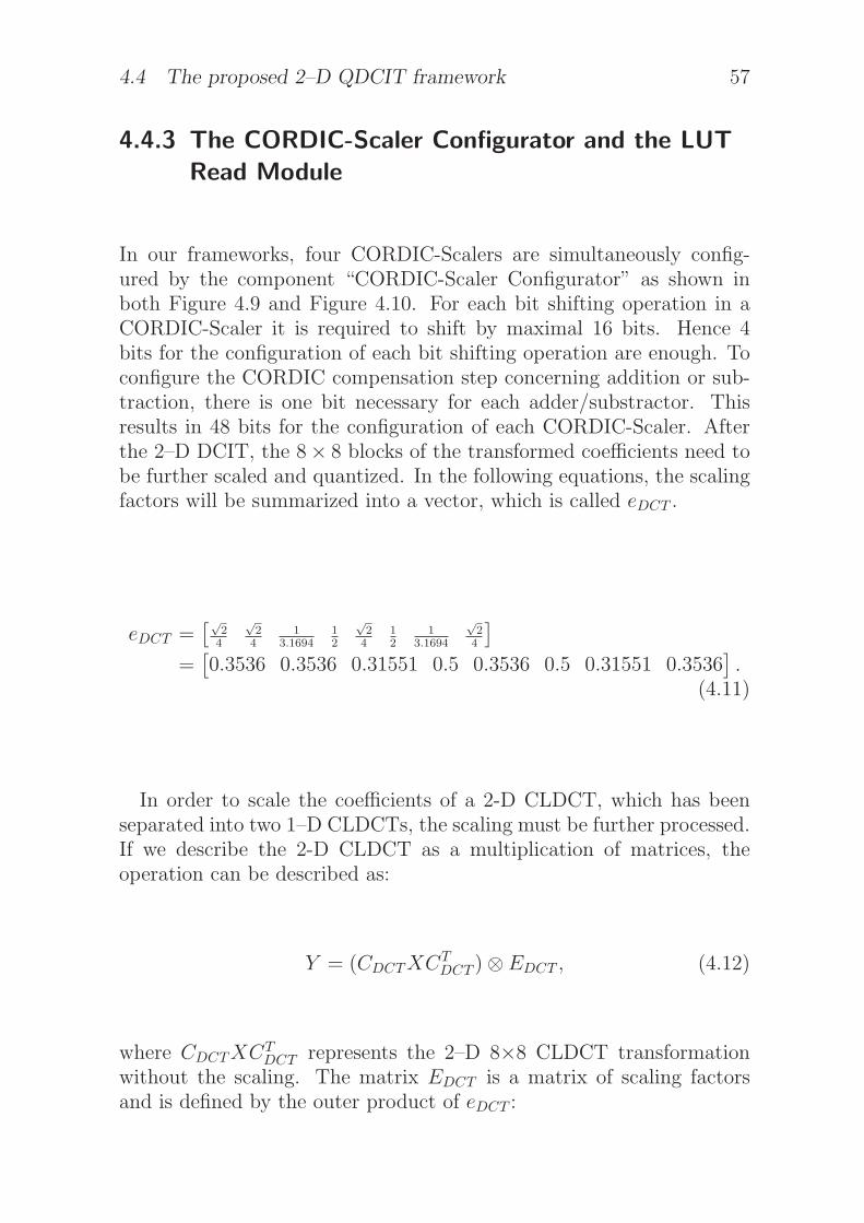
4.4 The proposed 2–D QDCIT framework 57
4.4.3 The CORDIC-Scaler Configurator and the LUT
Read Module
In our frameworks, four CORDIC-Scalers are simultaneously config-ured by the component “CORDIC-Scaler Configurator” as shown inboth Figure 4.9 and Figure 4.10. For each bit shifting operation in aCORDIC-Scaler it is required to shift by maximal 16 bits. Hence 4bits for the configuration of each bit shifting operation are enough. Toconfigure the CORDIC compensation step concerning addition or sub-traction, there is one bit necessary for each adder/substractor. Thisresults in 48 bits for the configuration of each CORDIC-Scaler. Afterthe 2–D DCIT, the 8× 8 blocks of the transformed coefficients need tobe further scaled and quantized. In the following equations, the scalingfactors will be summarized into a vector, which is called eDCT .
eDCT =[√
2
4
√2
4
1
3.16941
2
√2
4
1
2
1
3.1694
√2
4
]
=[
0.3536 0.3536 0.31551 0.5 0.3536 0.5 0.31551 0.3536]
.(4.11)
In order to scale the coefficients of a 2-D CLDCT, which has beenseparated into two 1–D CLDCTs, the scaling must be further processed.If we describe the 2-D CLDCT as a multiplication of matrices, theoperation can be described as:
Y = (CDCTXCTDCT )⊗ EDCT , (4.12)
where CDCTXCTDCT represents the 2–D 8×8 CLDCT transformation
without the scaling. The matrix EDCT is a matrix of scaling factorsand is defined by the outer product of eDCT :

58 Discrete Cosine Integer Transform (DCIT) 4
Table 4.4: LUT organization of an entry for Quantization of DCT coefficients
Fold Flag 1 Flag 2 Flag 3 Flag 4 X1/Y1 X2/Y2 X3/Y3 X4/Y4
4 Bits 1 Bit 1 Bit 1 Bit 1 Bit 4 Bits 4 Bits 4 Bits 4 Bits
EDCT = eTDCT × eDCT
=
0.125 0.125 0.112 0.176 0.125 0.176 0.112 0.1250.125 0.125 0.112 0.176 0.125 0.176 0.112 0.1250.112 0.112 0.099 0.158 0.112 0.158 0.099 0.1120.176 0.176 0.158 0.25 0.176 0.25 0.158 0.1760.125 0.125 0.112 0.176 0.125 0.176 0.112 0.1250.176 0.176 0.158 0.25 0.176 0.25 0.158 0.1760.112 0.112 0.099 0.158 0.112 0.158 0.099 0.1120.125 0.125 0.112 0.176 0.125 0.176 0.112 0.125
. (4.13)
If we take a closer look at the scaling matrix EDCT we can notice thatthere are only 6 different scaling factors: 0.125, 0.112, 0.176, 0.099, 0.158and 0.25, which means that only these 6 different scaling factors must bestored in lookup tables. In the current architecture, each scaling factorhas one lookup table, which contains the configuration of CORDIC-Scalers to scale with the respective value dependent on the QP. TheQP has a range from 1 to 31 for the DCT mode. Each entry of thetable contains 24 bits configuration data. Table 4.4 shows the structureof one single entry in the lookup table. Therefore, 6 tables for theDCT transformation contain in total 31×24×6=4464 bits. On the otherhand, the QPs of DC values in MPEG-4 are not linear as shown inTable 4.2. This results in only 28 possible combinations because thefirst four QPs are constant numbers. Hence we have created two morelookup tables for Luma DC values and Chroma DC values, respectively.The size of the Luma and Chroma tables are 28×24×2=1344 bits.
In the same way, there are only three scaling factors which are dif-ferent after the 2–D 4×4 integer transform: 0.25, 0.316 and 0.4. Soin the mode of the 4 × 4-integer transform, CORDIC-Scalers performa multiplication with the current scaling factors divided by the QPs,which have a range from 0 to 51. Similar to the 4 × 4 integer trans-form, there are 6 different scaling factors for the 8×8 integer transformwhich must be stored in the lookup tables: 0.125, 0.118, 0.158, 0.111,0.149, 0.2. If we take a closer look at Table 4.3 we can notice that the

4.4 The proposed 2–D QDCIT framework 59
Table 4.5: LUT organization of an entry for Quantization of 4 × 4/8 × 8-integertransform coefficients
Flags X1/Y1 X2/Y2 X3/Y3 X4/Y4 fold values 1...9
4 Bits 4 Bits 4 Bits 4 Bits 4 Bits 36 Bits
value of QStep doubles for each increment of 6. This means that foreach increment of 6 the configuration is the same except for the “Fold”value, which increases by 1. It is not necessary to store all combinationsin the lookup tables for each value of QP. It is enough to store only 6entries with the “Fold” values in order to reduce the size of the table.As there are 52 different values of QP there can be up to 9 incrementsof 6 for each value from 0 · · · 5. Hence for each entry there are 36 bitsnecessary for the fold. Table 4.5 shows how one entry in a table for theinteger transforms is organized. The size of the 4×4 and 8×8 integertransform tables are 6×56×9=3024 bits.
Therefore, 6 tables for DCT scaling factors and two further tables forLuma DC values and Chroma DC values are needed in MPEG-4, and9 tables are required for 4×4 and 8×8 integer transforms in H.264. Intotal 17 tables are required for the proposed architecture. In a similarway, for supporting the inverse transformation, the CORDIC–scaler canperform the scaling up and dequantization by regenerating the lookuptables.
The CORDIC-Scaler configurator will first get all the data from thecomponent “LookUp Table Read Module” and forward the relevant con-figuration to each CORDIC-Scaler. Figure 4.12 shows the inputs andoutputs of the CORDIC-Scaler configurator module and the LUT readmodule. First of all, there are two methods to configure the CORDIC-Scalers, dynamic or static. In the static case the configuration is variedwhen ever the value of QP changes. In the dynamic case the config-uration of the CORDIC-Scalers changes with the clock cycle, becausethe matrix of scaling factors contains different scaling factors for eachcolumn.
Since the architecture is pipelined, the CORDIC-Scalers have to beconfigured dynamically during each clock cycle. Of course, the overheadof hardware resources is higher compared to the static method due tothe extra registers for the buffering and the more complex scheduling
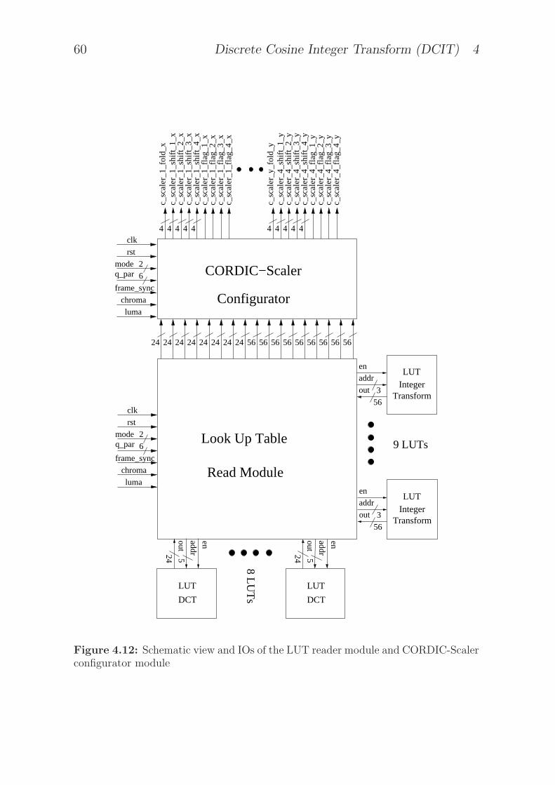
60 Discrete Cosine Integer Transform (DCIT) 4
rst
clk
luma
chroma
frame_sync
q_parmode
6
2
DCT
LUT
en
addr
out24 5
DCT
LUT
en
addr
out24 5
24 24 24 24 24 24 24 24 56 56 56 56
en
out
LUTInteger
Transform
addr
56
3
en
out
LUTInteger
Transform
addr
56
3
9 LUTs
CORDIC−Scaler
Configurator
Look Up Table
Read Module
rst
clk
luma
chroma
frame_sync
q_parmode
6
2
4 4 4 44
8 LUT
s
c_sc
aler
_y_f
old_
yc_
scal
er_4
_shi
ft_1_
yc_
scal
er_4
_shi
ft_2_
yc_
scal
er_4
_shi
ft_3_
yc_
scal
er_4
_shi
ft_4_
yc_
scal
er_4
_fla
g_1_
yc_
scal
er_4
_fla
g_2_
yc_
scal
er_4
_fla
g_3_
yc_
scal
er_4
_fla
g_4_
y
c_sc
aler
_1_f
old_
xc_
scal
er_1
_shi
ft_1_
xc_
scal
er_1
_shi
ft_2_
xc_
scal
er_1
_shi
ft_3_
xc_
scal
er_1
_shi
ft_4_
xc_
scal
er_1
_fla
g_1_
xc_
scal
er_1
_fla
g_2_
xc_
scal
er_1
_fla
g_3_
xc_
scal
er_1
_fla
g_4_
x4 4 4 4 4
56 56 56 56 56
Figure 4.12: Schematic view and IOs of the LUT reader module and CORDIC-Scalerconfigurator module

4.4 The proposed 2–D QDCIT framework 61
state machine for the configurations. The configuration signals contain48 bits per CORDIC-Scaler. Dependent on the mode and the chromaand the luma signals, the CORDIC-Scalers are configured.
These four CORDIC-Scalers are configured dynamically to process 8input values per clock cycle through a controller. This state machinewill first be triggered by the input signal “frame sync”. And then thestate machine will know that there is a new frame coming in and pre-pare to configure the CORDIC-Scalers. Before it starts to configurethe CORDIC-Scalers, it has to wait for 21 clock cycles until the firsttransformed input pixels arrive in the DCT mode. Similarly, for the4×4 integer transform 8 clock cycles are required and for the 8×8 inte-ger transform 16 clock cycles are required. After these delays, the statemachine will start to configure the CORDIC-Scalers, whose configura-tions change during each clock cycle. Note that the scaling inside aCORDIC-Scaler is separated into 5 stages, the fold and the 4 CORDICcompensation steps. Each of these stages is configured independentlyfrom the others.
4.4.4 The Post-Quantizer
For the forward transformation, the Post-Quantizer is required to per-form the remaining compensations after the CORDIC-Scalers. Thereare three cases for the Post-Quantizer stage. First, if the inputs arezeros, belong to DC values or in the integer transformation modes, itwill bypass them as indicated in Equation 4.8. Second, if the inputsbelong to the intra frame in the DCT mode, it will perform right shiftby 1 bit. Third, if the inputs belong to the inter frame in the DCTmode, it will perform left shift by 1 bit, minus one then right shift by2 bits for the reason explained in Equation 4.10. Figure 4.13 shows theschematic view of the Post-Quantizer. Note that the Post-Quantizer isnot required for the inverse transformation.

62 Discrete Cosine Integer Transform (DCIT) 4
15
in_6
sub 1 >> 2<< 1
>> 1
sub 1 >> 2<< 1
>> 1
sub 1 >> 2<< 1
>> 1
sub 1 >> 2<< 1
>> 1
sub 1 >> 2<< 1
>> 1
sub 1 >> 2<< 1
>> 1
sub 1 >> 2<< 1
>> 1
sub 1 >> 2<< 1
>> 1
15
in_2
15
in_4
15
in_5
15
in_7
out_0
15
out_2
15
out_1
15
out_3
15
out_4
15
out_5
15
out_6
1
out_7
15
frame_intra
15
in_0
15
in_1
15
in_3
clk mode
2
frame_syncrst
Figure 4.13: Schematic view of the Post-Quantizer

4.5 Experimental Results 63
Table 4.6: Complexity for each 2-D quantized transformation architecture
XXXXX
XXXX
XXX
TypeOperation
Mul Add W–Shift B–Shift Mux
Conventional Q+DCT [34] 40 52 8 0 0Novel QDCT [126] 32 52 8 0 0Novel QDCT (CSD) 0 308 224 72 0CORDIC based FQDCT 0 108 32 40 0CORDIC based FQDCIT (with integer transforms) 0 120 40 40 56CORDIC based FQDCIT (unshared) 0 268 60 120 8
4.5 Experimental Results
Table 4.6 summarizes the number of arithmetic units for each quan-tized architecture. At first, the conventional Q+DCT requires 40 mul,52 add and 8 shift operations to perform 2-D QDCT. For the 2-D NovelQDCT 32 mul, 52 add and 8 shift operations are required [126]. Therequired multiplications for both methods are not ideal for VLSI design.Even if we use the CSD representation to carry out the multiplications,the Novel QDCT still needs 302 add and 72 barrel shift operationsin the worst case. The presented 2-D Quantized CLDCT based onCORDIC architecture with four CORDIC-Scalers reduces the compu-tational complexity dramatically to 108 add operations. The number ofbarrel shifters is reduced, too. Furthermore, for integration of the 8×8and 4×4 integer transforms only 12 add, 8 barrel shift and 56 multiplexoperations are required additionally. Of course, the FQDCIT requiresextra multiplexers for performing the multi-functional transformations.However, the row “CORDIC based FQDCIT (unshared)” shows thecomplexity, if we implement the three quantized transformations with-out sharing hardware by using five configurable modules. It requiresmuch more arithmetic units compared to the shared one.

64 Discrete Cosine Integer Transform (DCIT) 4
Table 4.7: 2–D Transformation Complexity for arbitrary CORDIC iterations
Type/Operation Mul Add W–Shift B–Shift Mux
Novel IQDCT [126] 32 52 8 0 0scaled CORDIC DCT [139] 4 64 + 80×6 80×6 0 0CORDIC DCT/IDCT [116] 0 36 + 80×10 80×10 0 0CORDIC based DCT [62] 0 208 176 0 0CORDIC Loeffler DCT [112] 0 76 32 0 0IQDCIT–S1 0 92 24 24 44IQDCIT–S2 0 112 36 32 52IQDCIT (default) 0 124 40 40 60IQDCIT–C1 0 184 80 56 76
4.5.1 Variable Iteration Steps of CORDIC
Since the proposed IDCIT is executed based on the CORDIC algorithmiteratively, we can adjust the iterations of trigonometric operations inthe IDCIT (module 1–3) and the compensation steps of CORDIC-Scaleras different configurations. Table 4.7 lists the computational complex-ity if different number of CORDIC iterations are applied to the inversetransforms, where IQDCIT–S1 is a simplified version from the defaultIQDCIT with only 2 iterations/steps and IQDCIT–S2 has 2–3 itera-tions/steps. The number of iterations/steps is treated as a variable in-fluencing on the precision. On the other hand, IQDCIT–C1 extends thenumber of iterations to 6–8 iterations/steps in order to obtain a betterquality. For example, Figure 4.14 shows the configuration with differentCORDIC compensation steps for the default IQDCIT with 4 CORDICcompensation steps, IQDCIT–S1 with 2 steps and IQDCIT–C1 with 6steps. Note that the number of iteration is selected by the brute forcesearch with a target resolution. Clearly, the proposed IQDCIT not onlyreduces more than half arithmetic units than other regular CORDICDCTs but also executes the dequantization. In [116,139], besides addersfor butterfly operations and multipliers, additional CORDIC processorsare required. They assumed the DSP inside FPGA will satisfy the needfor CORDIC rotations. Therefore, additional number of shift and addoperations is required in here (80 shift–add operations for each pipelinedCORDIC with compensation steps as mentioned in Section 3.3).

4.5 Experimental Results 65
15
15
15
15
+/- +/-+/-
+/-
+/-Fold
F_yin
F_xin F_xout
F_yout+/-+/-+/-Fold
X3
Y3
X4
Y4Y2
X2
Y1
X1
(a) Flow graph of the default CORDIC-Scaler with 4 iterations
15
15
15
15
F_xout
F_yout
+/-
+/-
+/-Fold
F_yin
F_xin
+/-Fold
Y2
X2
Y1
X1
(b) Flow graph of the CORDIC-Scaler S1 with 2 iterations
15
15
15
15
F_xout
F_yout
+/-+/-
+/-
+/-Fold
F_yin
F_xin +/-+/-+/-
+/-+/-Fold +/-+/-+/-
X3
Y3Y2
X2
Y1
X1 X4
Y4
X5
Y5
X6
Y6
(c) Flow graph of the CORDIC-Scaler C1 with 6 iterations
Figure 4.14: Three flow graphs of CORDIC-Scaler with different number of CORDICcompensation steps
4.5.2 ASIC Implementation
A full-pipelined CORDIC based 2-D FQDCIT has been modeled inVHDL, including two 1-D DCITs, one transposition memory, four CORDIC-Scalers, one Post-Quantizer, one CORDIC-Scaler Configurator, one LUTreader and 17 dedicated lookup tables. Later, these RTL codes aresynthesized by Synopsys Design Compiler 2009 with TSMC 0.18µmstandard cell libraries. At the end, the final Place & Route stage is per-formed with the Cadence SoC Encounter 8.1 [19,117]. The final versionof the chip ready for fabrication is shown in Figure 4.15. Note that thetotal number of the IOs required for this design is 198 IO pads, whichwould result in a low chip density as in [71]. Hence we have to removethe IO pads and treat it as a macro IP design. The input and outputIOs are located in the left and lower side of the chip layout. Table 4.8lists the comparison between our final layout results and other availablecores in terms of several design criteria. Note that no further advancedmethodologies are introduced to improve the performance. Neverthe-less, a simple and straightforward pipelined design is presented (8–stagepipeline for the first 1–D DCIT, 8–stage pipeline for the transpose mem-ory, 8–stage pipeline for the second 1–D DCIT and 5–stage pipeline forthe CORDIC-Scaler). Figure 4.16 shows the timing waveform of the

66 Discrete Cosine Integer Transform (DCIT) 4
Figure 4.15: Final layout view of the 2–D CORDIC based FQDCIT implementationin TSMC 0.18µm technology library
post simulation in the mode of DCT transformation (QP=13) requiring29 clock cycles until the first pipeline outputs are ready.
There are some important points can be observed. First, we cansee that the proposed pipelined FQDCIT occupies small core size inchip area, because the CORDIC method enables a very simple architec-ture for implementation. For example, the core area is a little smallerthan [97], but the proposed core can achieve much higher throughputand supporting multi-functions for different Codecs. Note that inverseversion of the FQDCIT can be easily modified by reconfiguring themodules and flushing the lookup tables. Second, in [97] and [9], thecores achieve very high frequency by optimizing the pipeline stage (as-suming better arithmetic units), but provide very low throughput due
4.5 Experimental Results 67
to the serial output, i.e. one pixel per cycle. Contrary to the previousapproaches, the proposed one processes 8 samples in parallel per clockcycle, leading to a higher throughput, which is very suitable for Full–HD or even future 4K/8K UHD resolution [25,33]. This, however, doesnot lead to a very high increase in the chip area.
The latency is shorter than other designs due to the fine–gainedpipeline architecture. The critical timing delay is 7.121ns. Of course,we can further reduce the critical timing by replacing the default “Rip-ple Carry Adder” in current implementation by “Carry Save Adder”or “Carry Look-ahead Adder” for each pipelined stage [49]. On theother hand, the size of the core can be further shrieked if we remove thepipeline and folding the row-column decomposition as one single DCITand one CORDIC-Scaler with a buffer memory [9].
The presented implementation consumes more power than others dueto the higher operational frequency and the parallel output character-istic. However, synthesizing with the multiple voltage threshold libraryand the clock/power-gating methodology can help reduce the powerconsumption dramatically [67]. It can be reduced by slowing down theoperational frequency, too. Moreover, Dynamic Bit-width adaptation inDCT could also be applied into our design by decreasing the bit lengthof the high frequency coefficients [84]. The zero prediction algorithmcan also reduce the power consumption significantly by omitting the un-necessary computational efforts [63, 127, 140]. These two methods canreduce the computational efforts and power consumption by trading offthe transformation quality in PSNR. Finally, the VLSI implementationresults show that the presented CORDIC based QDCIT architecturecan provide a good solution for integration of different transformationsand their quantization methods by utilizing the CORDIC algorithm toshare the hardware resources.
4.5.3 Performance in MPEG–4 XVID and H.264
The proposed 2-D forward and inverse QDCIT transformations havebeen tested with the video coding standard MPEG–4 and H.264 byusing publicly available software, XVID Codec 1.2.2 [137] and JM-16.1 Codec [105]. The default DCT algorithm in the Codec of the

68 Discrete Cosine Integer Transform (DCIT) 4
0
13
88 8f ea 22 59 f0 0b e9 88 8f ea 22 59 f0 0b e9 53 48 da 84 63 fc 8e 23 de 31 2d 59 84 fd 70 56 6c b0
27 c9 c6 d3 df 06 bf aa 27 c9 c6 d3 df 06 bf aa 84 45 d1 2d 45 fe a0 05 01 13 52 62 ac 5f 17 d8 7d 75
bf d0 56 65 bb d3 38 2b bf d0 56 65 bb d3 38 2b fb b8 6e 33 57 03 06 c6 91 92 70 c1 97 2d 05 d5 b9 c9
37 24 51 4e 0d 57 1d 24 37 24 51 4e 0d 57 1d 24 4e 20 bc 07 8e 7c 13 62 32 cd 55 c8 35 82 43 d6 51 56
b3 1e 4c 9f 0e c5 d5 82 b3 1e 4c 9f 0e c5 d5 82 8b ea 77 4d 6c 72 ab fe 44 1c ce e7 d9 58 a0 69 f1 db
ee 90 25 96 b8 90 03 27 ee 90 25 96 b8 90 03 27 f4 c8 15 d3 bd c5 a8 40 9d 87 ad 62 24 d2 3f e7 08 df
bb 3c d0 ce 0b c1 60 8d bb 3c d0 ce 0b c1 60 8d 1e 47 16 c2 ef 75 87 b2 95 72 ba 23 8b 75 5d 72 34 ad
a1 03 39 b3 76 29 99 41 a1 03 39 b3 76 29 99 41 20 93 f8 ec b5 15 e1 9c cf af 32 83 1b 7f 86 3d 86 23
0 68 2 3 2 -6 -4
0 1 -1 -5 1
0 -2 -1 1 0
0 1 -4 -5 0 -1 0
0 -4 0 -1 -2 -3
0 1 -8 -2 2 -3
0 2 0 3 2 6
0 -3 0 1 -3 -1 -4
0 ns 50 ns 100 ns 150 ns 200 ns 250 ns 300 ns
clk
rst
mode 0
q_par 13
frame_sync
frame_intra
chroma
luma
in_0 88 8f ea 22 59 f0 0b e9 88 8f ea 22 59 f0 0b e9 53 48 da 84 63 fc 8e 23 de 31 2d 59 84 fd 70 56 6c b0
in_1 27 c9 c6 d3 df 06 bf aa 27 c9 c6 d3 df 06 bf aa 84 45 d1 2d 45 fe a0 05 01 13 52 62 ac 5f 17 d8 7d 75
in_2 bf d0 56 65 bb d3 38 2b bf d0 56 65 bb d3 38 2b fb b8 6e 33 57 03 06 c6 91 92 70 c1 97 2d 05 d5 b9 c9
in_3 37 24 51 4e 0d 57 1d 24 37 24 51 4e 0d 57 1d 24 4e 20 bc 07 8e 7c 13 62 32 cd 55 c8 35 82 43 d6 51 56
in_4 b3 1e 4c 9f 0e c5 d5 82 b3 1e 4c 9f 0e c5 d5 82 8b ea 77 4d 6c 72 ab fe 44 1c ce e7 d9 58 a0 69 f1 db
in_5 ee 90 25 96 b8 90 03 27 ee 90 25 96 b8 90 03 27 f4 c8 15 d3 bd c5 a8 40 9d 87 ad 62 24 d2 3f e7 08 df
in_6 bb 3c d0 ce 0b c1 60 8d bb 3c d0 ce 0b c1 60 8d 1e 47 16 c2 ef 75 87 b2 95 72 ba 23 8b 75 5d 72 34 ad
in_7 a1 03 39 b3 76 29 99 41 a1 03 39 b3 76 29 99 41 20 93 f8 ec b5 15 e1 9c cf af 32 83 1b 7f 86 3d 86 23
out_0 0 68 2 3 2 -6 -4
out_1 0 1 -1 -5 1
out_2 0 -2 -1 1 0
out_3 0 1 -4 -5 0 -1 0
out_4 0 -4 0 -1 -2 -3
out_5 0 1 -8 -2 2 -3
out_6 0 2 0 3 2 6
out_7 0 -3 0 1 -3 -1 -4
24 ns256 ns
232 ns
Figure 4.16: Timing waveform of the 2–D CORDIC based FQDCIT in the DCTmode (requiring 29 clock cycles for latency)

4.5Experim
ental
Resu
lts69
Table 4.8: Comparison of various DCT implementations and the proposed 2-D FQDCIT in different design criteria (area, timing,power, latency, throughput and architecture)
Year Function Tech Area(mm) Gates Power Frequency Gbits/sec Latency Architecture
Ours 8×8/4×4 FQDCIT 0.18um 1.8V 2.05 47.1(K) 269(mW) 125 MHz 15.0 29 cycles FGA TB Pipe PL
2007 [123] 8×8 DCT 0.18um 1.6V 1.32 N/A 4.08(mW) 80.6 MHz 0.967 N/A AIR RC TB Pipe
2006 [97] 8×8 DCT/IDCT 0.35um 3.3V 3.00 11.7(K) N/A 300 MHz 2.4 178 cycles FGA RC TB Pipe
2005 [71] 4×4 QInt 0.18um 1.8V N/A 51.6(K) N/A 68 MHz 10.3 N/A FGA Pipe PL
2005 [27] 8×8 DCT 0.18um 1.55V 0.12(Chip) N/A N/A 5 MHz 0.24 46 cycles FGA RC Pipe TB
2004 [40] 8×8 DCT 0.18um 2.16 N/A 7.5(mW) N/A 0.9 80 cycles AIR RC TBRAM
2004 [9] 8×8 DCT 0.18um 1.8V N/A 14.7(K) N/A 180 MHz 0.352 392 cycles MUXRC TB
2000 [22] 8×8 DCT 0.6um 2.0V 50.5 38(K) 138(mW) 100 MHz N/A 198 cycles DA PL
1998 [135] 8×8 IDCT 0.7um 1.3V 20.7(Chip) 40(K) 4.65(mW) 14 MHz 0.896 N/A RC TB Pipe
DA (Distributed Arithmetic), FGA (Flow-Graph Arithmetic), AIR (Algebraic Integer Representations), RC (Row–Column Decomposition),
MUXRC (Multiplexed Row–Column Decomposition), Pipe (Full Pipeline), PL (Parallel Architecture), TB (Transpose), TRAM (Transpose RAM).

70 Discrete Cosine Integer Transform (DCIT) 4
Table 4.9: The list of test sequences
video sequence frames resolution
foreman 300 CIF (352×288)paris 1065 CIF (352×288)news 300 CIF (352×288)crew 300 DVD (720×576)ice 240 DVD (720×576)rush hour 250 Full–HD (1920×1080)blue sky 217 Full–HD (1920×1080)
selected XVID implementation is based on Loeffler’s factorization usingfloating-point multiplications (see Figure 4.1) and MEPG–4 Quantiza-tion “method 2”. Both the NQDCT and the QDCIT are implementedin a System–C like style with fixed point shift–add operations into theXVID software and the H.264 JM-16.1 software. To test the perfor-mance of our configurations, video test sequences with CIF, DVD andFull–HD formats are used, where Table 4.9 lists all the test sequences,where the framerate is 60 FPS (original figures are attached in Ap-pendix B.5).
Figure 4.17 illustrates the average Peak Signal to Noise Ratio (PSNR)of the “foreman” and “paris” CIF video test sequences from low to highbitrates in XVID. The proposed architecture performs very close to theoriginal Forward Q+DCT design and almost the same as the ForwardNQDCT (FNQDCT). Figure 4.18 shows that the comparison resultsbetween the FQDCIT and the default method in H.264, where Int–4mode and Int–8 mode are compared separately. Obviously, the FQDCITarchitecture can obtain a good transformation quality. Note that thevideo sequences are first encoded with the FQDCIT architecture of thesetwo referenced softwares, then decoded by using the default decoder.
On the other hand, the inverse version has also been implementedwith different iteration numbers and compensation steps from Table 4.7,where Figure 4.19 illustrates the average PSNR of the “foreman”, “paris”and “news” CIF video test sequences from low to high bitrates in XVID.Obviously, these results agree with our expectation that the configura-tions with more shift and add operations or CORDIC iteration stepscan obtain better PSNR results. Moreover, the default “IQDCIT” is

4.5 Experimental Results 71
Figure 4.17: The average Forward Q+DCT, FNQDCT and FQDCIT PSNR of the“foreman” and “paris” cif video test from low to high bitrates in XVID
Figure 4.18: The average FQDCIT PSNR of the “foreman” and “paris” cif videotest from low to high bitrates in H.264
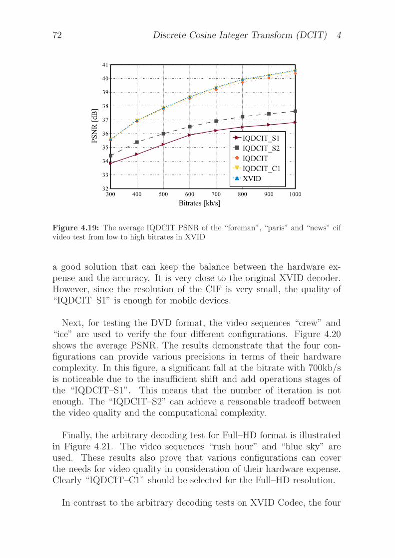
72 Discrete Cosine Integer Transform (DCIT) 4
Figure 4.19: The average IQDCIT PSNR of the “foreman”, “paris” and “news” cifvideo test from low to high bitrates in XVID
a good solution that can keep the balance between the hardware ex-pense and the accuracy. It is very close to the original XVID decoder.However, since the resolution of the CIF is very small, the quality of“IQDCIT–S1” is enough for mobile devices.
Next, for testing the DVD format, the video sequences “crew” and“ice” are used to verify the four different configurations. Figure 4.20shows the average PSNR. The results demonstrate that the four con-figurations can provide various precisions in terms of their hardwarecomplexity. In this figure, a significant fall at the bitrate with 700kb/sis noticeable due to the insufficient shift and add operations stages ofthe “IQDCIT–S1”. This means that the number of iteration is notenough. The “IQDCIT–S2” can achieve a reasonable tradeoff betweenthe video quality and the computational complexity.
Finally, the arbitrary decoding test for Full–HD format is illustratedin Figure 4.21. The video sequences “rush hour” and “blue sky” areused. These results also prove that various configurations can coverthe needs for video quality in consideration of their hardware expense.Clearly “IQDCIT–C1” should be selected for the Full–HD resolution.
In contrast to the arbitrary decoding tests on XVID Codec, the four

4.5 Experimental Results 73
Figure 4.20: The average IQDCIT PSNR of the “crew” and “ice” DVD video testfrom low to high bitrates in XVID
Figure 4.21: The average IQDCIT PSNR of the “rush hour” and “blue sky” Full–HDvideo test from low to high bitrates in XVID
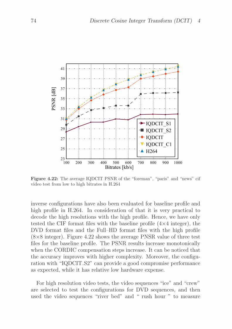
74 Discrete Cosine Integer Transform (DCIT) 4
Figure 4.22: The average IQDCIT PSNR of the “foreman”, “paris” and “news” cifvideo test from low to high bitrates in H.264
inverse configurations have also been evaluated for baseline profile andhigh profile in H.264. In consideration of that it is very practical todecode the high resolutions with the high profile. Hence, we have onlytested the CIF format files with the baseline profile (4×4 integer), theDVD format files and the Full–HD format files with the high profile(8×8 integer). Figure 4.22 shows the average PNSR value of three testfiles for the baseline profile. The PSNR results increase monotonicallywhen the CORDIC compensation steps increase. It can be noticed thatthe accuracy improves with higher complexity. Moreover, the configu-ration with “IQDCIT S2” can provide a good compromise performanceas expected, while it has relative low hardware expense.
For high resolution video tests, the video sequences “ice” and “crew”are selected to test the configurations for DVD sequences, and thenused the video sequences “river bed” and “ rush hour ” to measure

4.6 Summary 75
Figure 4.23: The average IQDCIT PSNR of the “crew” and “ice” DVD video testfrom low to high bitrates in H.264
the performance for Full–HD resolution. Figure 4.23 and Figure 4.24illustrate the performance for each, respectively. Obviously, all fourconfigurations show relative good performances. First, the results meetthe conclusion for CIF sequences that the more expensive configurationis, the better it performs. In total, these four configurations can pro-vide a balanced performance in terms of their hardware expense. TheIQDCIT-S1 and the IQDCIT-S2 fit for small resolutions or low bitrates.However, when the bitrates are high, IQDCIT and IQDCIT-C1 are pre-ferred. Therefore, these results agree with our expectation that theconfigurations with more shift–add operation stages/iteration steps canprovide better accuracy. Moreover, the configuration “IQDCIT” is agood solution that can keep the balance between the hardware expenseand the accuracy for both XVID and H.264 Codecs.
4.6 Summary
In this chapter, a low-complexity and highly-integrated QDCIT basedon the CORDIC architecture was presented. The proposed 2-D FQD-

76 Discrete Cosine Integer Transform (DCIT) 4
Figure 4.24: The average IQDCIT PSNR of the “rush hour” and “blue sky” Full–HDvideo test from low to high bitrates in H.264
CIT architecture requires only 120 add and 40 barrel shift operationsto perform the multiplierless 8×8 FQDCT and 4×4/8×8 forward quan-tized integer transform by sharing the hardware resources as much aspossible. The proposed design had been implemented with TSMC0.18µm cell library. On the other hand, an inverse version based onthe CORDIC algorithm with arbitrary iteration numbers had also beenimplemented. The proposed 2–D IQDCIT architecture requires only124 add and 40 barrel shift operations to perform the multiplierless8×8 IQDCT and quantized 4×4/8×8 inverse integer transform. Theproposed architecture can reduce more than half of the add operationscompared to the conventional Q+DCT and NQDCT architecture. Fur-thermore, it achieved a smaller chip area and higher throughput com-pared to the other architectures for future UHD resolution. Moreover,both XVID and H.264 simulations showed that the proposed QDCITarchitecture can provide a good compromise between PSNR and com-putational effort, and is also highly satisfactory compared to the refer-enced implementations in terms of video quality. Also note that usingarbitrary iteration steps can adjust the complexity of the architectureaccording to the target device’s resolution.
5 Parallel Jacobi Algorithm
In this chapter, a configurable Jacobi Eigenvalue Decomposition (EVD)array using a scaling–free µ–rotation CORDIC (µ–CORDIC) processoris presented in order to further study the tradeoff between the perfor-mance/complexity of processors and the load/throughput of intercon-nects. Computing the EVD in parallel with Jacobi’s iterative method isselected as an important example in this thesis, because the convergenceof this method is very robust to modifications of the homogeneous pro-cessor elements [18,46,47,70]. It is simple, concise and inherent parallelfor both implementation and computation. In [108,109], a Jacobi EVDarray was realized by implementing the µ–CORDIC processor, whichonly performs a predefined number of CORDIC iterations (e.g. only oneµ–rotation). In this way, the size of the processor array can be furtherreduced, such that a larger size of EVD array can be implemented. Inorder to further study the design impact in VDSM level, a 10×10 EVDarray (i.e. computing the EVD of a 20×20 symmetric matrix) was im-plemented in TSMC 45nm technology. After that, several modificationsof the algorithm/processor were studied and their impact on the designcriteria were investigated for different sizes of EVD array through a con-figurable interface (10×10 to 80×80). At the end, a strategy to complywith the design criteria is presented, especially in terms of balancingthe number of iterations and the computational complexity.
This chapter is organized as follows: serial and parallel Jacobi meth-ods will be described in Section 5.1. In Section 5.2 the design issues ofthe parallel Jacobi EVD array are discussed, which lead to the simplifi-cation from a regular Full CORDIC to the µ–CORDIC processor withadaptive number of iterations. Section 5.3 shows the implementationresults and Section 5.4 summarizes this chapter.
78 Parallel Jacobi Algorithm 5
5.1 Parallel Eigenvalue Decomposition
5.1.1 Jacobi Method
An eigenvalue decomposition of a real symmetric n×n matrix A is ob-tained by factorizing A into three matrices A = Q ∧ QT , where Q isan orthogonal matrix (QQT = I) and ∧ is a diagonal matrix whichcontains the eigenvalues of A. The Jacobi method approximates theeigenvalues iteratively as follows:
Ak+1 = QkAkQTk , with k = 0, 1, 2, . . . ,
(5.1)
where Qk is an orthonormal rotation by the angle θ in the (i, j) plane.It is an identity matrix containing four nonzero elements, qii = qjj =cos θk, and qij = −qji = sin θk:
Qk =
col i col j↓ ↓
1 0 · · · 0
0 . . .cos θk sin θk ← row i
... . . . ...− sin θk cos θk ← row j
. . . 00 · · · 1
(5.2)
The plane rotations Qk, where k = 0, 1, 2, · · · , can be executed invarious orders to obtain the ∧. The most common order of sequentialplane rotations {Qk} is called cyclic–by–row, i.e. (i, j) is chosen asfollows:
(i, j) = (1, 2)(1, 3) . . . (1, n)(2, 3) . . . (2, n) . . . (n− 1, n) . (5.3)
The execution of all N = n(n − 1)/2 index pairs (i, j) is called asweep. If several sweeps are applied, the matrix A will converge into a

5.1 Parallel Eigenvalue Decomposition 79
diagonal matrix ∧, which contains the eigenvalues λ1, λ2, . . . , λn:
limk→∞
Ak = diag[λ1, λ2, . . . , λn] =
λ1 0 · · · 0
0 λ2...
... . . . 00 · · · 0 λn
. (5.4)
Besides the cyclic–by–row order, many different sequential ordershave already been presented, such as butterfly–like permutation order-ing, odd-even ordering or dynamic ordering by searching the best rota-tion set [10–12]. These specialized orderings are chosen according to thetopology of network in order to guarantee good load balancing duringthe whole computational process. For example, for a parallel computerwith ring style network topology, the odd-even ordering should be se-lected for the goal of shortest path data transmission. However, theinfluence from the network topology on different orders becomes lessimportant due to the shorter timing delay between SoC processors, es-pecially when the packet–switched network is gradually replacing thebus transmission in large SoC systems. Therefore, the cyclic–by–roworder has been selected for the parallel EVD design.
5.1.2 Jacobi EVD Array
Instead of performing the plane rotations Qk one by one in a cyclic–by–row order, we can separate them into multi–subproblems and executethem in parallel on a (logn)–dimensional multi-core platform. A parallelarray for Jacobi’s method was first presented by Brent and Luk [18].It consists of n
2 × n2 homogeneous PEs and each PE contains a 2×2
sub-block of the matrix A. Figure 5.1 shows a typical 4×4 Jacobi EVDarray with 16 PEs. This Jacobi array can perform n
2 subproblems inparallel. Initially, each PE holds a 2×2 sub-matrix of A:
PEpq =
(
a2p−1,2q−1 a2p−1,2qa2p,2q−1 a2p,2q
)
, where p and q = 1, 2, · · · , n2 . (5.5)

80 Parallel Jacobi Algorithm 5
a65
a55 a56
a66 a67
a57 a58
a68
a85
a75 a76
a86 a87
a77 a78
a88
PE11 PE13
PE21 PE22
PE14
PE24PE23
PE44
PE34PE33PE31
PE41 PE42 PE43
PE12
PE32
Figure 5.1: A 4×4 EVD array, where n=8 for 8×8 symmetric matrix
A rotation angle has to be choosen in order to zero the off–diagonalelements of the submatrix by solving a 2×2 symmetric EVD subproblemas shown in the following:
[
a′ii a′ija′ji a′jj
]
= R ·[
aii aijaji ajj
]
· RT ,
where R =
[
cos θ − sin θsin θ cos θ
]
.
(5.6)
We obtain the maximal reduction {a′ij, a′ji} = 0 by applying the op-timal angle of rotation θopt:
θopt =12 arctan(
2aijajj−aii ), (5.7)
where the range of θopt is limited to |θopt| ≤ π4 .
This optimal angle θopt, which can annihilate the off–diagonal ele-ments (a2p−1,2q and a2p,2q−1), is computed by diagonal PEs using Equa-tion 5.7. After these rotation angles are computed, they will be sent tothe off–diagonal PEs. This transmission is indicated by the dashed linesin the vertical and horizontal direction in Figure 5.1. All off–diagonalPEs will perform a two-sided rotation with the corresponding rotationangles who are obtained from the row (θr) and column (θc) respectively.
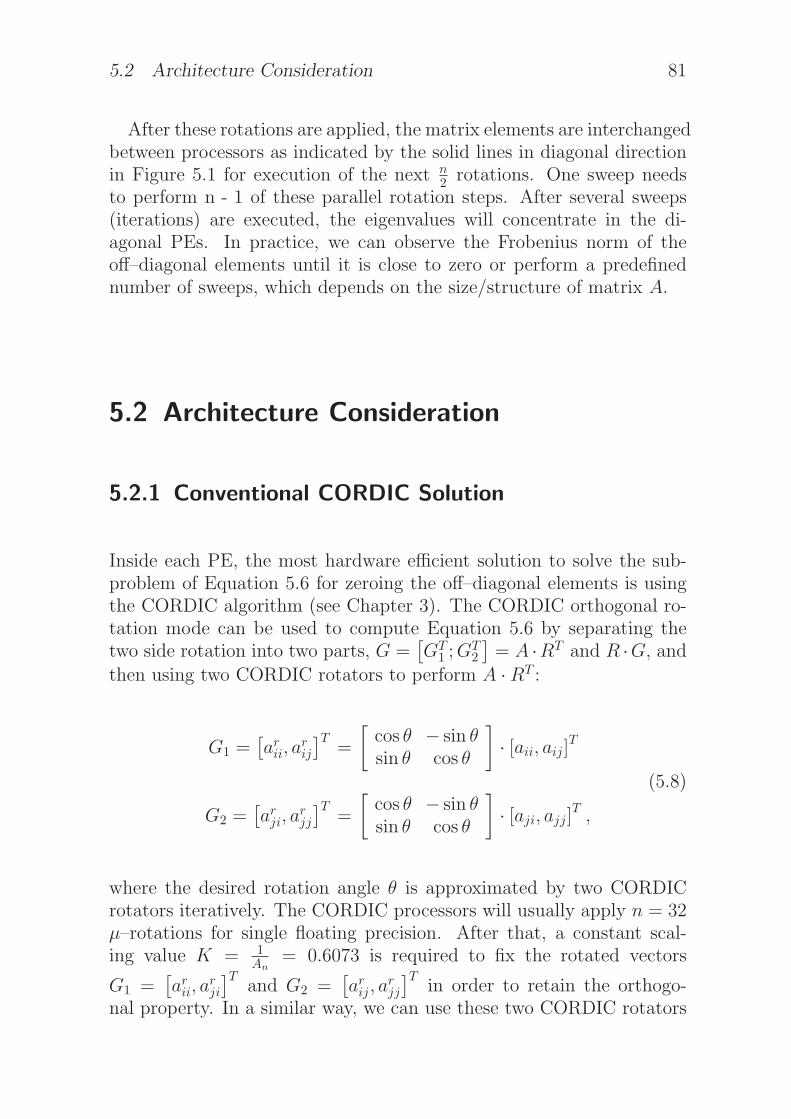
5.2 Architecture Consideration 81
After these rotations are applied, the matrix elements are interchangedbetween processors as indicated by the solid lines in diagonal directionin Figure 5.1 for execution of the next n
2 rotations. One sweep needsto perform n - 1 of these parallel rotation steps. After several sweeps(iterations) are executed, the eigenvalues will concentrate in the di-agonal PEs. In practice, we can observe the Frobenius norm of theoff–diagonal elements until it is close to zero or perform a predefinednumber of sweeps, which depends on the size/structure of matrix A.
5.2 Architecture Consideration
5.2.1 Conventional CORDIC Solution
Inside each PE, the most hardware efficient solution to solve the sub-problem of Equation 5.6 for zeroing the off–diagonal elements is usingthe CORDIC algorithm (see Chapter 3). The CORDIC orthogonal ro-tation mode can be used to compute Equation 5.6 by separating thetwo side rotation into two parts, G =
[
GT1 ;G
T2
]
= A ·RT and R ·G, and
then using two CORDIC rotators to perform A ·RT :
G1 =[
arii, arij
]T=
[
cos θ − sin θsin θ cos θ
]
· [aii, aij]T
G2 =[
arji, arjj
]T=
[
cos θ − sin θsin θ cos θ
]
· [aji, ajj]T ,(5.8)
where the desired rotation angle θ is approximated by two CORDICrotators iteratively. The CORDIC processors will usually apply n = 32µ–rotations for single floating precision. After that, a constant scal-ing value K = 1
An= 0.6073 is required to fix the rotated vectors
G1 =[
arii, arji
]Tand G2 =
[
arij, arjj
]Tin order to retain the orthogo-
nal property. In a similar way, we can use these two CORDIC rotators

82 Parallel Jacobi Algorithm 5
to compute R ·G:
[
a′
ii, a′
ji
]T=
[
cos θ − sin θsin θ cos θ
]
·[
arii, arji
]T
[
a′
ij, a′
jj
]T=
[
cos θ − sin θsin θ cos θ
]
·[
arij, arjj
]T.
(5.9)
Meanwhile, the optimal rotation angle can be also approached byusing the CORDIC orthogonal vector mode (see Table 3.1). The θoptangle can be approximated iteratively as: 2× θopt = arctan(
2aijajj−aii ).
In VLSI design, there are two common ways to realize the CORDICdependence flow graph in hardware, the folded (serial) or the parallel(pipelining) as earlier described in Section 3.3. Note that we restrictonly to the conventional CORDIC iteration scheme as mentioned inEquation 3.15. Although the folded CORDIC flow graph consumesmore energy than the pipelined CORDIC, it is still selected here inorder to satisfy the need for large EVD array computation. Figure 5.2(a)shows a folded CORDIC PE. It requires a pair of adders for the planerotation and another adder for steering the next angle direction, which isidentical to Figure 3.3. However, after the plane rotation, the remainingscaling procedure has to be further proceeded by the Figure 5.2(b) forfixing the An, where two multiplexers are required for selecting theinputs to the barrel shifters for CORDIC compensation steps. Thisfolded dependence graph is typical for the orthogonal rotation mode andbenefits in a small area in VLSI design. Moreover, it requires a numberof different shifts according to the chosen shift sequence, additionalbarrel shifters are required in folded CORDIC architecture for successiverecursive processing.
In practice, the angle accumulator is not required for the off–diagonalPEs. We can directly use the di from Equation 3.15 to steer the rotators.This means that the transmission on the dashed lines in the vertical andhorizontal direction in Figure 5.1 will be replaced by a sequence of diflags. In this way, the computation effort for the θopt can be omitted.

5.2 Architecture Consideration 83
adder or substractor
buffer register
right shift k bit
2x1 multiplexer
Look-Up Table
(b) Rotating
add
add
(b) Scaling
add
add
Reg
add
>>k
Reg
Reg
Reg
Reg
Reg
>>k
>>k
>>k
>>k
mux
ROM
add
ROMROM
di
zout
yout
xoutx0
y0
z0
−di
−di
mux
mux
mux
yout
xoutx0
y0
−di
mux
mux
di
Figure 5.2: Flow graph of a folded CORDIC (recursive) processor with the scaling
5.2.2 Simplified µ–rotation CORDIC
In this subsection, the methodology how to simplify the regular CORDICarchitecture will be clarified. As the process technologies continue toshrink to the VDSM level, it becomes possible to directly implementa full parallel Jacobi EVD array [3, 72]. However, the size of EVD ar-ray with the regular CORDIC that could be implemented on currentdevice is still small. Therefore, it is necessary to simplify the architec-ture in order to integrate more processors for solving larger matrices.A scaling–free µ–CORDIC for performing the plane rotation in Equa-tion 5.6 is used, where the number of inner iterations is reduced (from32 iterations to only one iteration [46, 70]). Here, the µ–CORDIC willbe implemented as a circuit and verified under different design criteria(area, timing, power/energy).
The definition of µ–CORDIC can be developed from Equation 3.15as:
xi+1 = m[
xi − yi · di · 2−i]
yi+1 = m[
yi + xi · di · 2−i]
m =√
cos2 θ + sin2 θ = 1 + ǫ,
(5.10)
where m is the required scaling factor per iteration and ǫ is the off-set error. The idea of µ–CORDIC rotation is to reduce the number of
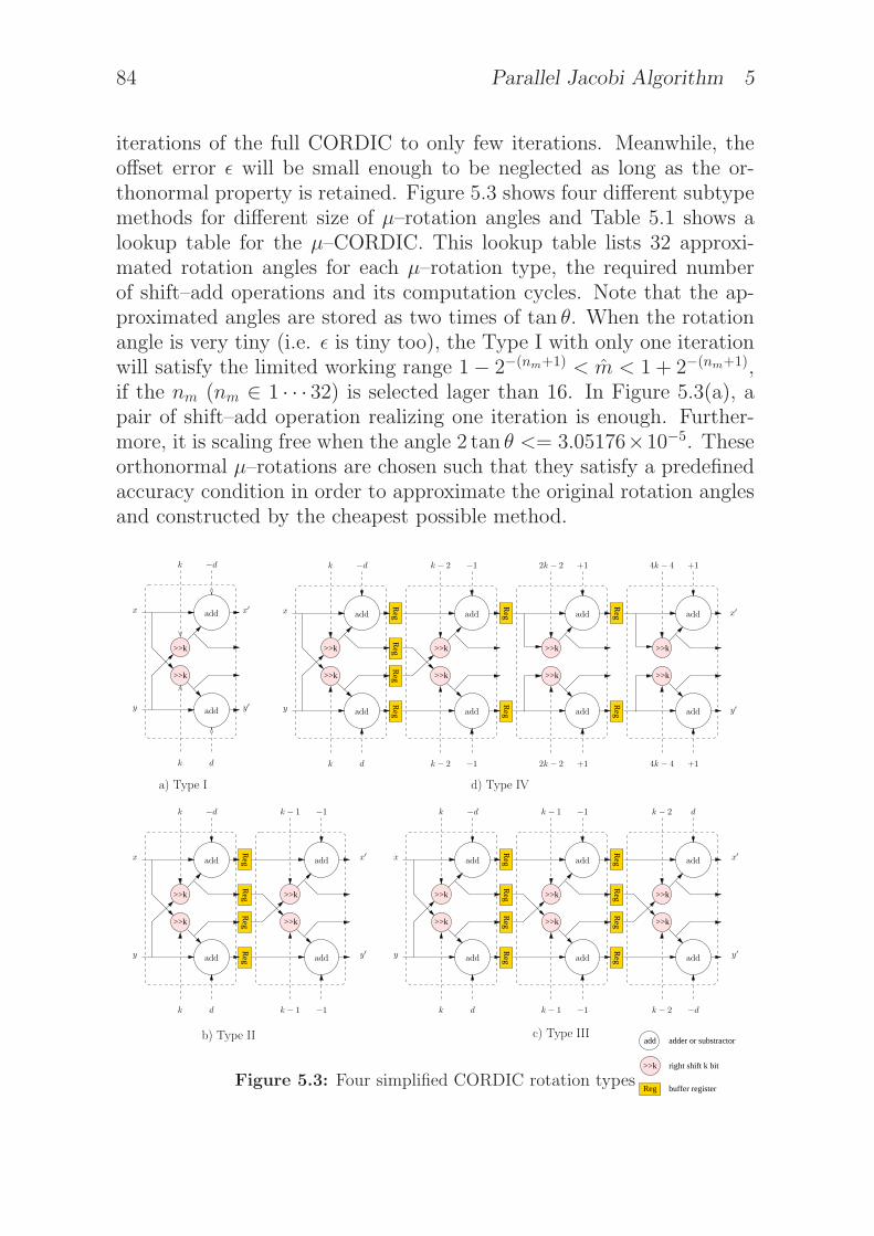
84 Parallel Jacobi Algorithm 5
iterations of the full CORDIC to only few iterations. Meanwhile, theoffset error ǫ will be small enough to be neglected as long as the or-thonormal property is retained. Figure 5.3 shows four different subtypemethods for different size of µ–rotation angles and Table 5.1 shows alookup table for the µ–CORDIC. This lookup table lists 32 approxi-mated rotation angles for each µ–rotation type, the required numberof shift–add operations and its computation cycles. Note that the ap-proximated angles are stored as two times of tan θ. When the rotationangle is very tiny (i.e. ǫ is tiny too), the Type I with only one iterationwill satisfy the limited working range 1− 2−(nm+1) < m < 1 + 2−(nm+1),if the nm (nm ∈ 1 · · · 32) is selected lager than 16. In Figure 5.3(a), apair of shift–add operation realizing one iteration is enough. Further-more, it is scaling free when the angle 2 tan θ <= 3.05176×10⁻⁵. Theseorthonormal µ–rotations are chosen such that they satisfy a predefinedaccuracy condition in order to approximate the original rotation anglesand constructed by the cheapest possible method.
buffer register
right shift k bit
adder or substractor
>>k
>>k
Reg
Reg
Reg
Reg
>>k
>>k
>>k
>>k
Reg
Reg
Reg
Reg
Reg
Reg
Reg
Reg
>>k
>>k
>>k
>>k
>>k
>>k
>>k
>>k
Reg
Reg
Reg
Reg
Reg
Reg
Reg
Reg
Reg
add
>>k
>>k
>>k
>>k
>>k
>>k
>>k
x′
y′
a) Type I
add
add
x
y
k
k −d
d
x′
y′
k − 1 −1
k − 1 −1
add
add
b) Type II
add
add
x
y
k
k −d
d
add
add
x
y
k
k −d
d
k − 2 −1
k − 2 −1
add
add
d) Type IV
4k − 4 +1
4k − 4 +1
add
add
2k − 2 +1
2k − 2 +1
add
add
x′
y′
x′
y′
add
add
x
y
k
k −d
d
k − 1 −1
k − 1 −1
add
add
k − 2 d
k − 2 −d
add
add
c) Type III
Figure 5.3: Four simplified CORDIC rotation types

5.2 Architecture Consideration 85
Next, for the µ–rotation Type II as shown in Figure 5.3(b), when thenm is selected from 8 to 15, two pairs of shift–add operations are enoughto retain the orthonormal property. Moreover, when the nm is selectedfrom 5 to 7, Type III repeats three times µ–rotation without any scaling.Finally, for large rotation angles, the offset errors cannot be omittedwithout scaling. Figure 5.3(d) shows the corresponding dependenceflow graph for Type IV. Besides two pairs of shift–add operations forrotation itself at the beginning of the sub flow graph, 2∼4 pairs ofshift–add operations are required to fix the scaling factor m:
m = (1 + 2−2(k+1))(1 + 2−4(k+1)) · · · (1 + 2−2M (k+1)). (5.11)
Note that the scaling costs M=2∼4 pairs of shift–add operations. Ingeneral, we can say that the cost of Type IV is given by 2+M pairs ofshift–add operations. For example, when the index k is 2, the scalingis:
m2 = (1 + 2−6)(1 + 2−12)(1 + 2−24). (5.12)
These four subtypes have three identical parts: Type I with one it-eration, the scaling part of Type IV and the second iteration of TypeII. These three parts can be integrated together by using multiplexersto select the data paths as shown in Figure 5.4, which has 2 adders,2 shifters and 4 multiplexers. More detailed information about the µ–CORDIC can be found in [46, 108].
5.2.3 Adaptive µ–CORDIC iterations
To improve the computational efficiency, we perform 6 iterations percycle and name it CORDIC–6. Since the global clock in a synchronouscircuit is determined by the longest path, which also means that themaximum timing delay per iteration is 6 cycles (when the index k is 1,Type IV). Therefore, the inner iteration steps are repeated until theyare close to the critical one. The required numbers of repetition arequoted in Table 5.1. For example, when the rotation angle index isk=8, it will repeat three times from the index k=8 to the index k=10.When the rotation angle index is k=20, it will repeat six times fromthe index k=20 to the index k=25. On the other hand, the number ofiterations can be adjusted by selecting the average angle during the last

86 Parallel Jacobi Algorithm 5
2 5 32 32
8
8
32
32
32
32 32
32
adder or substractor
buffer register
right shift k bit
2x1 multiplexer
Controller
>>k
>>k
Reg
Reg
Reg
Reg
Reg
>>k
add
mux
mux
mux
mux
add
add
x′a
x′
y′a
y′
x
dy
kx
ky
mux
dx
xa
y
ya
type index xin yin en
yout
xout
S0 S1
Figure 5.4: The block diagram of a scaling–free µ–CORDIC PE, including 2 adders,2 shifters and 4 multiplexers
sweep and name it as CORDIC–mean. In this way, the iteration stepsof adaptive µ–CORDIC are defined according to the structure of thematrix.
5.2.4 Exchanging inner and outer iterations
Modifying the inner iteration number of CORDIC processor will causea tradeoff issue. Decreasing the iterations will result in an increasednumber of outer sweeps due to the imprecise inner iterations. Therefore,the Full CORDIC architecture requires fewer sweeps but needs morearea. On the other hand, the simplified µ–CORDIC architecture canreduce the area but results in an increased number of outer sweeps.This problem becomes a tradeoff between the iteration numbers and thecomputational complexity. In the next section, we will further comparethese rotation modes in Matlab.
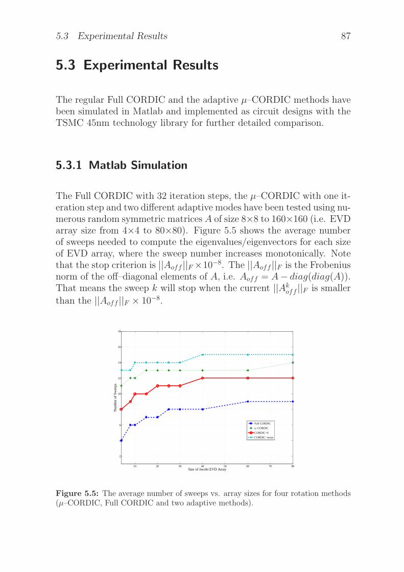
5.3 Experimental Results 87
5.3 Experimental Results
The regular Full CORDIC and the adaptive µ–CORDIC methods havebeen simulated in Matlab and implemented as circuit designs with theTSMC 45nm technology library for further detailed comparison.
5.3.1 Matlab Simulation
The Full CORDIC with 32 iteration steps, the µ–CORDIC with one it-eration step and two different adaptive modes have been tested using nu-merous random symmetric matrices A of size 8×8 to 160×160 (i.e. EVDarray size from 4×4 to 80×80). Figure 5.5 shows the average numberof sweeps needed to compute the eigenvalues/eigenvectors for each sizeof EVD array, where the sweep number increases monotonically. Notethat the stop criterion is ||Aoff ||F×10−8. The ||Aoff ||F is the Frobeniusnorm of the off–diagonal elements of A, i.e. Aoff = A− diag(diag(A)).That means the sweep k will stop when the current ||Ak
off ||F is smaller
than the ||Aoff ||F × 10−8.
10 20 30 40 50 60 70 80
2
4
6
8
10
12
14
16
18
Size of Jacobi EVD Array
Num
ber
of S
wee
ps
Full CORDIC
u−CORDIC
CORDIC−6
CORDIC−mean
Figure 5.5: The average number of sweeps vs. array sizes for four rotation methods(µ–CORDIC, Full CORDIC and two adaptive methods).

88 Parallel Jacobi Algorithm 5
When the Jacobi EVD array size is 10×10, the µ–CORDIC requires12 sweeps while the Full CORDIC only requires 6 sweeps. If we adjustthe inner rotations to six times, the sweep number will be 10, smallerthan the µ–CORDIC but more than the Full CORDIC. On the otherhand, using the average rotation angle to decide the rotation numberas CORDIC–mean will require more sweeps than the others. Althoughthe µ–CORDIC requires twice more sweeps per EVD computation thanthe Full CORDIC, it actually reduces the number of the inner CORDICrotations, which results in an improved computational complexity. Forexample, a 10×10 array with the Full CORDIC PE needs 6 sweeps× 32 inner CORDIC rotations, the CORDIC–6 needs 10 sweeps × 6inner CORDIC rotations, while the µ–CORDIC PE only requires 12sweeps × 1 inner CORDIC rotation. In Figure 5.6, the average shift–add operations required for each rotation method with different size oftesting EVD arrays is demonstrated, where Full CORDIC needs muchmore shift–add operations than others and the adaptive CORDIC–6method can offer a compromise between the hardware complexity andthe computational effort. Consequently, from an algorithmic point ofview, doubtless we would prefer to realize the Jacobi method by utilizingthe µ–CORDIC method. However, when it comes to nanoscale VLSIimplementation, other design issues become also important.
Figure 5.7 shows the off–diagonal Frobenius norm versus the sweepnumbers. When the array size is 10×10 with double floating precision,each rotation method will easily converge to the predefined stop cri-terion. Here the stop criterion is also defined as ||Aoff ||F × 10−8. Ina similar situation, when the array size is 80×80 as illustrated in Fig-ure 5.8, the convergence is also obtained. However, when using thesingle floating precision (default IEEE 754 single), it will no longer con-verge due to the insufficient operand precision.
Figure 5.9 and Figure 5.10 show the reduction of the off–diagonalFrobenius norm versus the sweep numbers for single floating precision.It can be noticed that the off–norms do not reach the convergence.Each size of EVD array has its own stop criterion (maximum offNormreduction vs. sweep number). Therefore, we must first analyze theFrobenius norm of the off–diagonal elements in Matlab and then observeit until it reaches its maximal reduction. Afterwards, a lookup table hasto be generated and directly assigned these stop criteria to the targethardware circuit or IP component.

5.3 Experimental Results 89
10 20 30 40 50 60 70 8010
4
105
106
107
108
109
1010
Size of Jacobi EVD Array
Num
ber
of S
hitf
and
Add
ope
ratio
ns
Full CORDIC
u−CORDIC
CORDIC−6
CORDIC−mean
Figure 5.6: The number of shift–add operations for four rotation methods on differ-ent size of array
5.3.2 Using threshold methods
In Figure 5.9 and Figure 5.10, the decrease of the off–diagonal normbecomes slower with single floating precision, it is obvious that the ro-tations along these plateaus do not contribute to the overall result forsmall rotation angles. A simple way to reduce such inefficient oper-ations is to apply a threshold strategy. That means in each sweep athreshold value is used to decide if a rotation is computed or not. Thethreshold method was already mentioned by Wilkinson in [128]. Heworked with a fixed sequence of threshold values, lowering from sweepto sweep to reduce computation time. Every transformation regardingan off–diagonal element that is below the threshold value is bypassed.However, there is a problem for comparing floating point numbers incircuit design. Since the design complexity of the floating comparator issame as the floating adder, the benefit we could obtain from the simpli-fied µ–CORDIC will become oblivious. Therefore, another simple wayto predict the index E is presented in here, which came from m×2E−127,where m is the mantissa and E is the exponent of an IEEE 754 singlefloating point number. Figure 5.12 shows the frequency distribution of

90 Parallel Jacobi Algorithm 5
1 2 3 4 5 6 7 8 9 10 11 12 13 14 1510
−7
10−6
10−5
10−4
10−3
10−2
10−1
100
101
102
Sweep
Off
Nor
m
Full CORDIC
u−CORDIC
CORDIC−6
CORDIC−mean
Figure 5.7: The required number of sweeps vs. off–diagonal norm for 10×10 JacobiEVD array with double floating precision
the optimal rotation angle θopt’s exponent E over the sweep number fora Jacobi EVD array of size 10×10 in single floating precision. Addi-tionally, Figure 5.13 shows the frequency distribution for the array sizeof 80×80.
It can be noticed that both average peaks appear in a range from127 to 96 (equal to 0 to -32). It is very similar to the rotation indexn = 32 for both Full CORDIC and µ–CORDIC. In order to simplify thecomparator operations, this prediction can be utilized to bypass thosesmall rotation angles which have very little contribution to the conver-gence. Figure 5.11 further shows the reduction of shift–add operationswith the threshold strategy and the preconditioned E index method ondifferent size of the array in IEEE 754 single floating precision. If theregular Full CORDIC is selected, a maximal reduction up to 40% can beachieved. For the µ–CORDIC and CORDIC–6, a reduction up to 10%of shift–add operations is obtained. Therefore, using the preconditionedE index method not only achieves a similar reduction of shift–add op-erations compared to the threshold strategy (sometimes even better),but also replaces the floating comparators by a lookup table.

5.3 Experimental Results 91
1 2 3 4 5 6 7 8 9 10 11 12 13 14 1510
−6
10−5
10−4
10−3
10−2
10−1
100
101
102
103
104
Sweep
Off
Nor
m
Full CORDIC
u−CORDIC
CORDIC−6
CORDIC−mean
Figure 5.8: The required number of sweeps vs. off–diagonal norm for 80×80 JacobiEVD array with double floating precision
5.3.3 Configurable Jacobi EVD Array
One of the major contributions in this thesis is to design a configurableJacobi EVD interface, where a n×n (n = 2, 4, 8, . . . , 2k, k ∈ N) parallelsystolic processor array can be generated through the C++ program di-rectly as long as there is enough logic for implementation. In Figure 5.1,it can be easily noticed that there are similar interconnection propertiesbetween the neighbor PEs in this 4×4 systolic array. Essentially, thesePEs can be categorized into six different types which are highlighted bydashed boxes in Figure 5.14. These six different types can help discoverthe similar property coding style for parameters design, especially inthe data switching behavior between the neighbor PEs. According totheir locations, they are “top”, “bottom”, “inner”, “left”, “right” andfour “corner”. The pseudo code for each type is listed in AppendixTable A.2.
In theory, once the off–diagonal elements of matrixA are small enoughor the computation reaches the predefined maximal sweep number ac-cording to the Matlab analysis, then the systolic processor array will
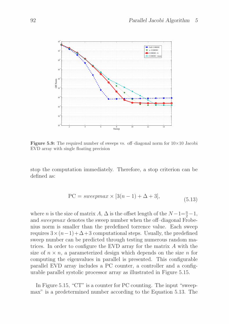
92 Parallel Jacobi Algorithm 5
2 4 6 8 10 12 1410
−7
10−6
10−5
10−4
10−3
10−2
10−1
100
101
102
Sweep
Off
Nor
m
Full CORDIC
u−CORDIC
CORDIC−6
CORDIC−mean
Figure 5.9: The required number of sweeps vs. off–diagonal norm for 10×10 JacobiEVD array with single floating precision
stop the computation immediately. Therefore, a stop criterion can bedefined as:
PC = sweepmax× [3(n− 1) + ∆ + 3],(5.13)
where n is the size of matrix A, ∆ is the offset length of the N−1=n2−1,
and sweepmax denotes the sweep number when the off–diagonal Frobe-nius norm is smaller than the predefined torrence value. Each sweeprequires 3×(n−1)+∆+3 computational steps. Usually, the predefinedsweep number can be predicted through testing numerous random ma-trices. In order to configure the EVD array for the matrix A with thesize of n × n, a parameterized design which depends on the size n forcomputing the eigenvalues in parallel is presented. This configurableparallel EVD array includes a PC counter, a controller and a config-urable parallel systolic processor array as illustrated in Figure 5.15.
In Figure 5.15, “CT” is a counter for PC counting. The input “sweep-max” is a predetermined number according to the Equation 5.13. The

5.3 Experimental Results 93
1 2 3 4 5 6 7 8 9 10 11 12 13 14 1510
−6
10−5
10−4
10−3
10−2
10−1
100
101
102
103
104
Sweep
Off
Nor
m
Full CORDIC
u−CORDIC
CORDIC−6
CORDIC−mean
Figure 5.10: The required number of sweeps vs. off–diagonal norm for 80×80 JacobiEVD array with single floating precision
signal “off” is the stop flag. The signal “stop” tells the parallel sys-tolic array when to stop the computation. The signal “store” notifiesthe eigenvalues are ready for transmission to the output ports. The in-structions for controlling the PEs are identical, if their ∆ are equal too.There are N lines for “store” and “stop” singles to notify the N parallelsubproblems. Note that the signal “loads” has 6 different instructions.One “load” instruction is for diagonal PEs. There are N − 1 “loadt”instructions, N 2−N “loada11” instructions, N 2−N “loada12” instruc-tions, N 2−N “loada21” instructions and N 2−N “loada22” instructionsfor off-diagonal PEs. These six instructions will notify the PEs whento load the input matrix, transmit the output eigenvalues/eigenvectoror exchange the matrix elements with its neighbors.
For instance, when the single“LW” is asserted, the matrix A will firstbe assigned to the array through the “input” ports. Once “enable” isasserted, the EVD array will start to compute the eigenvalues. Afterseveral sweep rotations, if the “pc in” is equal to the “sweepmax”, itwill stop the computation. The diagonal PEs will forward the results tothe output ports. So far we assumed the n should be even for simplicity.

94 Parallel Jacobi Algorithm 5
4 8 10 15 20 25 30 40 60 800%
5%
10%
15%
20%
25%
30%
35%
40%
45%
Size of Jacobi EVD Array
Red
uctio
n of
Shi
tf an
d A
dd o
pera
tions
Full CORDIC (th)
Full CORDIC (E)
u−CORDIC (th)
u−CORDIC (E)
CORDIC−6 (th)
CORDIC−6 (E)
Figure 5.11: The reduction of shift–add operations (in percent) for three rotationmethods with the threshold strategy and preconditioned E index on different size ofarray in IEEE 754 single floating precision
For odd n we can simply expand the matrix A by zeros.
5.3.4 Circuit Implementation
The presented µ–CORDIC has been modeled and compared with thefolded Full CORDIC in VHDL. Later, these two methods are imple-mented into parallel EVD arrays with size 4×4 and 10×10 through aconfigurable interface separately. After that, they are synthesized bythe Synopsys Design Compiler with TSMC 45nm standard cell library.It should be noticed that the word-length is 32 bits for IEEE 754 singlefloating precision. At the end, the SoC Encounter is used to perform thePlace & Route. Figure 5.16 shows the chip layout with 100 µ–CORDICPEs. We did not add any IO pads to the implementation and treatedit as a standard macro design. Table 5.2 lists the synthesis results forarea, timing delay and power consumption.
First of all, the combinational logic area and the power consumptionof the µ–CORDIC PE is much smaller than for the Full CORDIC.Furthermore, in order to determine the time required to compute theEVD of a n× n symmetric matrix, we obtain:

5.3 Experimental Results 95
85
90
95
100
105
110
115
120
125
130
12
34
56
78
910
1112
1314
15
0
1000
2000
3000
4000
5000
6000
IEEE 754 exponet
20x20 u−CORDIC
Sweep
Figure 5.12: 3–D bar statistic view of the l = E − 127 index for adaptive indexselection for 10×10 Jacobi EVD array with single floating precision
85
90
95
100
105
110
115
120
125
130
12
34
56
78
910
1112
1314
15
0
1
2
3
4
x 105
IEEE 754 exponet
160x160 u−CORDIC
Sweep
Figure 5.13: 3–D bar statistic view of the l = E − 127 index for adaptive indexselection for 80×80 Jacobi EVD array with single floating precision
Ttotal = Tdelay ×Kiteration ×Ksweep × [3(n− 1) + ∆ + 3],n = 8, 16, 20, 30, . . . 160,∆ = n
2 − 1.(5.14)
The total timing delay per EVD operation is defined as “ the criti-cal timing delay × the number of inner CORDIC rotations × averagenumber of outer sweeps × size of the matrix A”. We can observe thatthe total operation time is dependent upon the relation between theinner CORDIC rotations and the outer sweeps. For instance, comput-

96 Parallel Jacobi Algorithm 5
PE11 PE13
PE21 PE22
PE14
PE24PE23
PE44
PE34PE33PE31
PE41 PE42 PE43
PE12
PE32
∆=0
∆=0
∆=0
∆=0
∆=1
∆=2
∆=3
∆=1
∆=1
∆=1
∆=1
∆=1
∆=2
∆=2
∆=2
∆=3
Figure 5.14: The locations of six different PE types in a 4×4 Jacobi EVD array
LW
Counter
clk
rst
enable
sweepmax
offpc_inPC
input
Parameterized EVD array
Configurable
NN
stop
stor
e
load
s N+4N(N-1)
Controller
N×N Arrayn×32bits
(n×n matrix)n×n×32bits
Figure 5.15: A configurable parallel Jacobi EVD design
ing the EVD on the 10×10 EVD array with the Full CORDIC, requires4.286×32×7×(3×19+9+3) ∼= 66.24 us. Using the µ–CORDIC PE onlyrequires 2.247×2×10×(3×19+9+3) ∼= 3.1 us. Therefore, a speed upby a factor of 21.4 can be obtained from reducing the number of innerCORDIC rotations. Although the reduction of power consumption isnot so much due to extra multiplexers, µ–CORDIC’s controller and alookup table, it actually consumes much less energy per EVD compu-tation due to the shorter computation time. Note that the µ–CORDICPE requires two inner iterations in average due to the different rotationcycles (from six to one inner iteration) as shown in Table 5.1. Therefore,we can incorporate the synthesis results from Table 5.2 and the precon-ditioned E index to normalize the energy consumption with different

5.3 Experimental Results 97
Figure 5.16: Final layout view of a 10×10 Jacobi EVD array with the µ–CORDICPE with TSMC 45nm technology library.
size of EVD array. Figure 5.17 shows the predicted energy consumptionresults for size of the array from 4×4 to 80×80. Note that the energyconsumption is shows on the logarithmic scale on the Y–axis. Bothrotation methods consume much less energy than the Full CORDIC,where the CORDIC–6 can obtain an energy reduction factor of 40.9and the µ–CORDIC can obtain an energy reduction factor of 104.3 inaverage compared to the Full CORDIC. In short, the µ–CORDIC notonly achieves less combinational logic cell area and faster frequency,but also less energy consumption compared to the Full CORDIC. Onthe other hand, the CORDIC–6 consumes two times more energy thanthe µ–CORDIC, but the convergence speed is faster. Therefore, thisbecomes a tradeoff issue between the µ–CORDIC and the CORDIC–6(computation time vs. energy consumption).

98 Parallel Jacobi Algorithm 5
Figure 5.17: The energy consumption per EVD operation with each size of EVDarray (operating at 100 MHz)
5.4 Summary
Computing the EVD by the parallel Jacobi method was selected as atypical example due to its robust convergence property. A configurableJacobi EVD array has been implemented with both Full CORDIC andµ–CORDIC to explain the design concepts for parallel iterative algo-rithms. Using the preconditioned E index method not only reducedmore than 35% shift–add operations for the Full CORDIC and 10% forthe µ–CORDIC in average, but also omits the floating point numbercomparators. Afterwards, for a TSMC 45nm implementation, a detailedcomparison between area, timing delay and power/energy consumptionwas made. It was shown that the modification of inner iterations notonly reduced the size of the combinational logic, improved the overallcomputation time but also saved the energy consumption. Furthermore,the CORDIC–6 provided a compromised solution between the compu-tation time and the energy consumption compared to the µ–CORDIC.
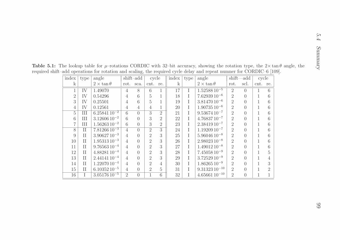
5.4Summary
99
Table 5.1: The lookup table for µ–rotations CORDIC with 32–bit accuracy, showing the rotation type, the 2× tan θ angle, therequired shift–add operations for rotation and scaling, the required cycle delay and repeat numner for CORDIC–6 [109].
index type angle shift–add cycle index type angle shift—add cyclek 2× tan θ rot. sca. cnt. re. k 2× tan θ rot. scl. cnt. re.
1 IV 1.49070 4 8 6 1 17 I 1.52588 10−5 2 0 1 62 IV 0.54296 4 6 5 1 18 I 7.62939 10−6 2 0 1 63 IV 0.25501 4 6 5 1 19 I 3.81470 10−6 2 0 1 64 IV 0.12561 4 4 4 1 20 I 1.90735 10−6 2 0 1 65 III 6.25841 10−2 6 0 3 2 21 I 9.53674 10−7 2 0 1 66 III 3.12606 10−2 6 0 3 2 22 I 4.76837 10−7 2 0 1 67 III 1.56263 10−2 6 0 3 2 23 I 2.38419 10−7 2 0 1 68 II 7.81266 10−3 4 0 2 3 24 I 1.19209 10−7 2 0 1 69 II 3.90627 10−3 4 0 2 3 25 I 5.96046 10−8 2 0 1 610 II 1.95313 10−3 4 0 2 3 26 I 2.98023 10−8 2 0 1 611 II 9.76563 10−4 4 0 2 3 27 I 1.49012 10−8 2 0 1 612 II 4.88281 10−4 4 0 2 3 28 I 7.45058 10−9 2 0 1 513 II 2.44141 10−4 4 0 2 3 29 I 3.72529 10−9 2 0 1 414 II 1.22070 10−4 4 0 2 4 30 I 1.86265 10−9 2 0 1 315 II 6.10352 10−5 4 0 2 5 31 I 9.31323 10−10 2 0 1 216 I 3.05176 10−5 2 0 1 6 32 I 4.65661 10−10 2 0 1 1

100
ParallelJacob
iAlgorithm
5
Table 5.2: Area, Delay and Power Consumption results of 4×4 and 10×10 Jacobi EVD arrays with the TSMC 45nm technology.
4×4 Full CORDIC 4×4 µ–CORDIC 10×10 Full CORDIC 10×10 µ–CORDIC
AreaCombinational 0.847 mm2 0.296 mm2 5.143 mm2 1.829 mm2
Noncombinational 0.390 mm2 0.123 mm2 2.306 mm2 0.833 mm2
Total 1.237 mm2 0.419 mm2 7.449 mm2 2.662 mm2
Power
Cell 62.283 mW 18.239 mW 388.379 mW 123.215 mWNet 0.465 mW 0.433 mW 2.993 mW 2.678 mWLeakage 11.909 mW 3.765 mW 86.136 mW 23.966 mWTotal 74.657 mW 22.437 mW 477.508 mW 149.859 mW
TimingCritical 4.454 ns 1.213 ns 4.286 ns 2.247 nsFrequency 224.5 MHz 824.4 MHz 233.3 MHz 445 MHz

6 Sparse Matrix–VectorMultiplication on Network–on–Chip
A new concept for accelerating Sparse Matrix–Vector Multiplication(SMVM) operations by using Network–on–Chip (NoC) is introducedin this chapter. In traditional circuit design on-chip communicationshave been designed with dedicated point-to-point interconnections orshared buses. Therefore, regular data transfer is the major concern ofmany parallel implementations. However, when dealing with the paral-lel implementation of SMVM, which is the main step of most iterativealgorithms for solving systems of linear equations, the required datatransfers are usually dependent on the sparsity structure of the matrixand can be extremely irregular. Using a NoC architecture makes itpossible to deal with an arbitrary structure of the data transfers. Inthis chapter, a configurable SMVM calculator based on the NoC archi-tectures (SMVM–NoC) is implemented with arbitrary size of p × p(p = 2, 4, 8, . . . , 2k, k ∈ N) with the IEEE-754 single floating point pre-cision in an FPGA.
This chapter is organized as follows: In Section 6.1, a brief introduc-tion to recent works on SMVM will be given first. After that, Section 6.2shows the main concept of the parallel NoC based SMVM architecture.Then, the hardware implementation will be described in Section 6.3 indetail. In Section 6.4, the experimental results are given. Section 6.5summarizes this chapter.

102 Sparse Matrix–Vector Multiplication on Network–on–Chip 6
6.1 Introduction of Sparse Matrix–VectorMultiplication
Over the past 30 years, researchers and scientists have tried variousapproaches to mitigate the poor performance of sparse matrix compu-tations, such as reordering the data to diminish wasted memory band-width, modifying the algorithms to reuse the data, and even buildingspecialized memory controllers. Despite these efforts, the sparsity ofthe matrices still dominates the performance of the SMVM computa-tions [81].
SMVM is used in many applications. For example, Finite ElementMethod (FEM) is a widely applied engineering analysis tool which isbased on obtaining a numerically approximate solution for a given math-ematical model of a structure. The resulting linear system is char-acterized by the system matrix A which is usually large and sparse[29,37,83,98]. In general, iterative solvers, such as the Conjugate Gra-dient (CG) method, are almost dominated by SMVM operations (usu-ally more than 95%). The CG method is the most popular iterativemethod for numerically solving a system of linear equations, A · x = b,where A is a Symmetric Positive-Definite (SPD) sparse matrix [52,77].Moreover, Google’s PageRank (PR) Eigenvalue problem is consideredto be the world’s largest sparse matrix calculation. This problem is alsodominated by SMVM operations where the target matrix is extremelysparse, and unstructured.
In the last decade, many researchers were dealing with the integra-tion of pipelining and parallelism inherent in the SMVM computationin hardware designs. Sun et al. [114] proposed a SMVM design con-taining many Processing Elements (PEs) with pipelined floating-pointunits in FPGA. Gregg et al. [39] built a specialized memory controllerto accelerate the SMVM. Gotze and Schwiegelshohn [48] presented asystolic algorithm which allows the parallel execution of SMVM in adedicated VLSI circuit. Williams et al. [129] used multi-core environ-ment, using the heterogeneous x86 based quad-core CPU to acceleratethe SMVM computation in parallel. Google’s PR problem has also beeninvestigated for acceleration with FPGA in [76, 141].

6.2 SMVM on Network-on-Chip 103
Conventional SMVM architectures are usually focused on a dedicatedinternal chip interconnection to forward vector components and nonzeromatrix elements among several processors. For instance, the fat-treestyle design, which requires pre-sorting and pre-ordering before the datainput [65], will become extremely difficult when the matrix is very largeand sparse. This motivates to use a packet–switched network for solvingthese design issues. This packet switching architecture is called NoC asearlier described in Section 2.3.
In this chapter, an FPGA accelerator for SMVM–NoC architectureis presented in order to solve the design problems which arise fromlarge sparse matrices with their extremely irregular structures. Thebasic idea of this concept is to implement an on-chip internal networkas the main transmission bone for the data transfers required for theSMVM computation. The presented vision provides a superior methodto handle large sparse matrices, especially it can deal with arbitrarysparsity structures. The 2×2, 4×4 and 8×8 SMVM-NoC calculatorshave been implemented on Xilinx Virtex-6 platform. According to theimplementation results, utilizing the packet forwarding functionality isbeneficial concerning heterogeneous IP integration and flexibility.
6.2 SMVM on Network-on-Chip
6.2.1 Sparse Matrix-Vector Multiplication
A typical SMVM operation can be expressed as follow:
A · x = b, (6.1)
where x and b are vectors of length n and A is a n × n sparse matrix.Since the matrix A can be very large and sparse, iterative solvers aretypically used to solve the system of linear equations due to their lowstorage requirements [45]. Many researchers have already utilized thepipelining and the parallelism to improve the performance. However,the computational complexity is still determined by the sparsity of thematrix A [29].

104 Sparse Matrix–Vector Multiplication on Network–on–Chip 6
In practice, the sparse matrix is usually stored in a CompressedSparse Row (CSR) format, in which only the nonzero matrix elementswill be stored in contiguous memory locations. In CSR format, thereare three vectors: val for nonzero matrix elements; col for the columnindex of the nonzero matrix elements; and ptr stores the locations inthe val vector that start a new row [141]. As an example, consider asimple SMVM operation with 5×5 sparse matrix A as follows:
4 0 8 0 06 0 3 0 00 1 0 0 00 0 0 5 07 0 0 0 4
·
x1x2x3x4x5
=
b1b2b3b4b5
. (6.2)
The CSR format of this matrix can be described by three vectorsgiven below:
————————————–val: 4 8 6 3 1 5 7 4
————————————–col: 1 3 1 3 2 4 1 5
————————————–ptr: 1 3 5 6 7 8
————————————–
When a CSR format matrix is read in successively, the column indexof the nonzero element can be obtained from col, while the row indexis indirectly indicated by ptr. This format can be easily facilitated intothe data packets for a switching network.

6.2 SMVM on Network-on-Chip 105
−20−10
010
20 −20
−10
0
10
20
−1000
0
1000
2000
3000
x2
x1
f(x
)=
1 2x
TA
x−bT
x+
c
Figure 6.1: The quadratic surface of the f(x)
6.2.2 Conjugate Gradient Solver
CG iterative solver, which was presented in 1952 by Magnus Hestenesand Eduard Stiefel [52], is perhaps the best known iterative method usedfor solving very large and extremely sparse systems of linear equations.The starting point in the derivation is to consider how we might be ableto minimize the quadratic function: f(x) = 1
2xTAx− bTx+ c, where c ∈
R, b ∈ Rn and A ∈ R
n×n is assumed to be a SPD matrix. The minimumvalue of f(x) is −bTA−1b/2, achieved by setting x = A−1b. Therefore,minimizing f(x) and solving A · x = b are equivalent problems. Forexample, when we define them as:
A =
[
3 22 6
]
, b =
[
2−8
]
and c = 0, (6.3)
we obtain a (n+1)–dimensional convex parabolic surface as illustratedin Figure 6.1. Minimizing f(x) corresponds to the solution for A ·x = b.That means the solution is the lowest point on the surface, which canbe obtained by using the steepest descent method [45].
However, when the condition of A increases, the steepest descentmethod will barely converge to the solution. A better approach is touse A-conjugate direction for the descent. Algorithm 1 briefly describes

106 Sparse Matrix–Vector Multiplication on Network–on–Chip 6
a simple scenario of the CG algorithm. This while loop approximatesthe next value of x (estimated solution), r (residual) and p (search di-rection) iteratively. Each iteration step will yield a better x by “walkingdownhill” in the A-conjugate direction of vector p. A convergence test,as idealized by the while clause set, causes the CG algorithm to ter-minate if the residual r vector is smaller than the predefined tolerancevalue. More than 95% of the computational efforts are SMVM opera-tions: q ⇐ Apk [29].
Algorithm 1 Conjugate Gradient Algorithm [45]Require: A is n× n SPD matrix, x and b are vectors of length n.Ensure: Congate(A, x, b, tol)x(0) ⇐ x0 initial guessp(0) ⇐ r(0) ⇐ b⇐ Ax(0)
k ⇐ 0while (norm(rk) ≥ tol ) doq ⇐ Apk (SMVM operation)α⇐ (rk, rk)/(pk, q)x(k+1) ⇐ xk + αpk
r(k+1) ⇐ rk − αqβ ⇐ (r(k+1), r(k+1))/(rk, rk)p(k+1) ⇐ r(k+1) + βpk
k ⇐ k + 1end while
6.2.3 Basic Idea
In order to accelerate the performance of the iterative solvers, a SMVMplatform was built based on the NoC architecture according to the ear-lier reports [110, 111], which contains p × p PEs (p = 2, 4, 8, . . . , 2k
k ∈ N). It is connected by a 2–D mesh network. The packet forwardingfunction is used to transmit the data.
For instance, Figure 6.2 shows a simple scenario (see Equation 6.2)for mapping a parallel SMVM–NoC computation. The circle symbolsdenote the nonzero elements from the sparse matrix, the square symbolsdenote the vector elements, and the rhombus symbols denote the results,respectively. First of all, the vector components xj have already been

6.2 SMVM on Network-on-Chip 107
assigned to PE according to the predefined routing addresses. Afterthat nonzero matrix elements Aij will be distributed to the correspond-ing PE according to the coordinate index i and j through the meshnetwork; i.e. vector x1 arrives at the PE with A11, A21, and A51 ele-ments, vector x2 arrives at the PE with A32 element, vector x3 arrivesat the PE with A13 and A23 elements, vector x4 arrives at the PE withA44 element, and vector x5 arrives at the PE with A55 element in the
network, respectively. Now the partial products b(j)i = Aij · xj must
be computed and then the b(j)i are accumulated to form bi =
∑
b(j)i .
Note that the number of nonzero elements nz is usually larger than thenumber of PEs. The detailed mapping method will be explained inSection 6.3.6.
Figure 6.2: A direct mapping of parallel SMVM operations based on the NoC ar-chitecture
On the other hand, we can also reverse the first and second step sothat nonzero matrix elements Aij will be distributed to the PE arraybefore broadcasting the vector components xj. This inverse mappingis shown in Appendix Figure B.6. In this way, dense matrix problemcan be handled when the number of nonzero matrix elements is farmore than the vector components. This, however, does not lead to anymodification of the proposed architecture, because this could be doneby using the MicroBlaze to modify the packet’s headers. For reason ofsimplicity at beginning, the first scenario is selected.
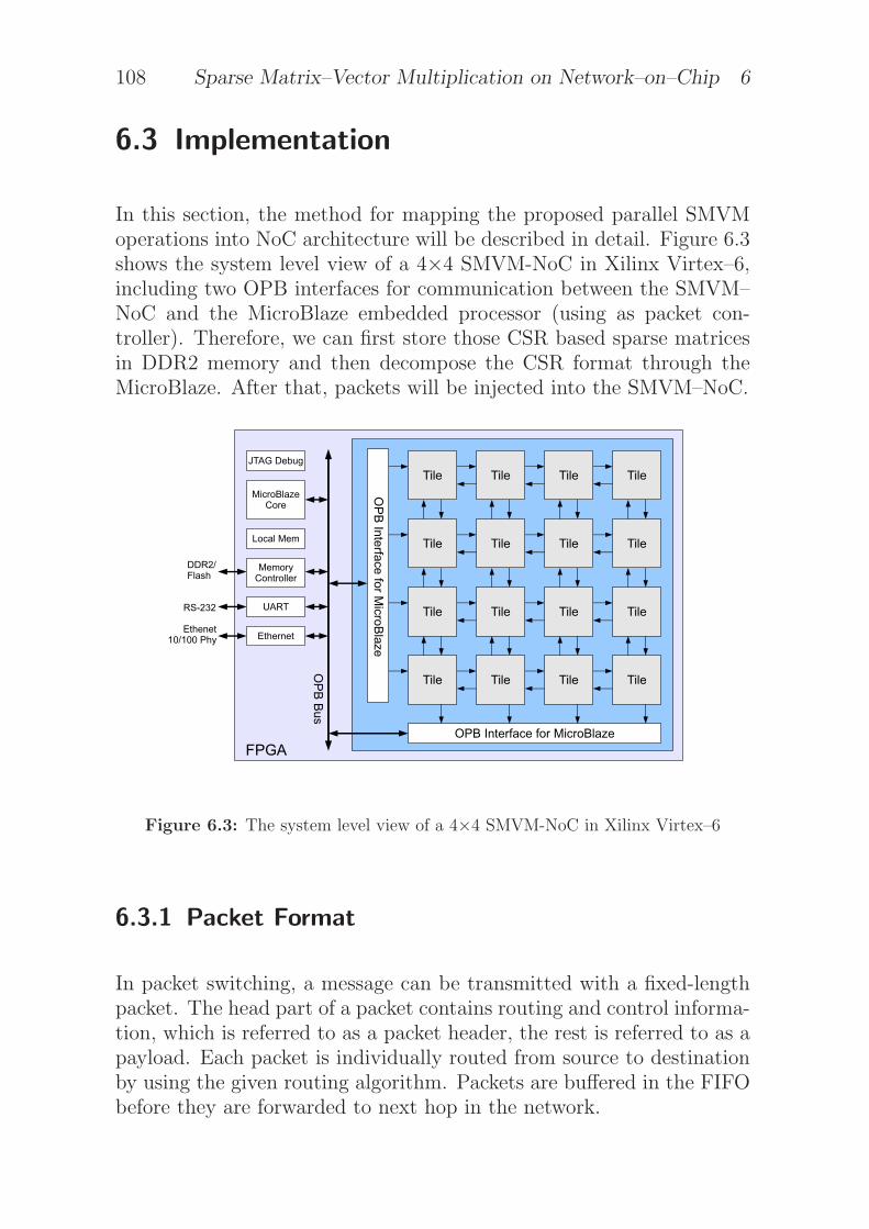
108 Sparse Matrix–Vector Multiplication on Network–on–Chip 6
6.3 Implementation
In this section, the method for mapping the proposed parallel SMVMoperations into NoC architecture will be described in detail. Figure 6.3shows the system level view of a 4×4 SMVM-NoC in Xilinx Virtex–6,including two OPB interfaces for communication between the SMVM–NoC and the MicroBlaze embedded processor (using as packet con-troller). Therefore, we can first store those CSR based sparse matricesin DDR2 memory and then decompose the CSR format through theMicroBlaze. After that, packets will be injected into the SMVM–NoC.
Figure 6.3: The system level view of a 4×4 SMVM-NoC in Xilinx Virtex–6
6.3.1 Packet Format
In packet switching, a message can be transmitted with a fixed-lengthpacket. The head part of a packet contains routing and control informa-tion, which is referred to as a packet header, the rest is referred to as apayload. Each packet is individually routed from source to destinationby using the given routing algorithm. Packets are buffered in the FIFObefore they are forwarded to next hop in the network.

6.3 Implementation 109
Table 6.1: Packet Format
Bit Functionality
50 Finish flag49 OPCode:0⇒Multiplication and 1⇒Accumulation48 DataType:0⇒Matrix and 1⇒Vector
40-47 Y–Coordinate32-39 X–Coordinate0-31 Payload
The packet format that is used to communicate over the proposedNoC architecture is summarized in Table 6.1. The packet is mainlyconstituted by the header and the payload. The header contains threeflags and two addresses. The three flags are named Finish, OPCode, andDataType. The Finish flag tells the routers that this packet containsthe result of the SMVM operation and needs to be forwarded to theMicroBlaze controller through the exit port. The OPCode informs thePE which floating-point operation (i.e. multiplication or accumulation)is going to be performed, and the DataType flag represents the type ofinput data (i.e. matrix element or vector element). The objective oftwo addresses (i.e. X–Coordinate and Y–Coordinate) is to locate theposition of the PE for the multiplier or the accumulator.
6.3.2 Switch Architecture
The switch is the most important component concerning the NoC per-formance. However, the area and the power consumption are also im-portant design criteria for embedded systems. For this reason, a con-ventional 5×5 crossbar switch is now separated into two small 3×3crossbar switches in order to reduce the area overhead [68]. Figure 6.4illustrates a typical switch component for the local PE to communicatewith its neighbor PEs consists of a set of input/output ports, dual-crossbar switches, four input FIFOs and controllers. The switch hasfive data input ports and five data output ports, named North, East,West, South, and Local, respectively. The Local port is connected toits PE, and the North, East, West, South ports are connected to themesh network.

110 Sparse Matrix–Vector Multiplication on Network–on–Chip 6
Figure 6.4: Detailed switch interconnection including two 3×3 crossbars, five I/Oports and four FIFOs
Each packet needs at least four cycles for transmitting a packet tonext hop. In the first cycle, the PE will read a packet from the FIFOand then decomposes the packet in the second cycle.
The packet will be routed in the third cycle. If the desired port isavailable the packet will be output, otherwise it will wait until the out-put port is free. Here the Round-Robin strategy is selected to preventthe deadlock hazard when multiple packets arrive in a switch at thesame time [35]. This switching approach is usually known as the store–and–forward method. It is a packet switching protocol in which thenode stores the complete packet and forwards it based on the informa-tion within its header. Thus the packet may stall if the router in theforwarding path does not have enough buffer space [16]. However, forthe simple and easy implementation of the presented SMVM–NoC inthe FPGA, store–and–forward routing is preferred at beginning.
On the other hand, wormhole switching combines packet switchingwith the data streaming quality of circuit switching to achieve a min-
6.3 Implementation 111
imal packet latency. In here the packets are divided into many smallflits. The router will first check the header of the packet for determin-ing the next hop and immediately forward it. The subsequent flits arealso forwarded as they arrive. This causes the packet to worm its waythrough the network. Flits are acting like ants, hence gave the name.However, when a stalling happens, this method has an unpleasantlyexpensive side effect of occupying all the links that the worm spans.Furthermore, virtual cut–through has a forwarding mechanism similarto the wormhole switching. However, before forwarding the first flit,the node waits for a guarantee that the next hop in the path will acceptthe entire packet. Thus if the packet stalls, it collects and waits at thecurrent node without blocking any links. Of course, the performance ofwormhole switching method and virtual cut–through method are bet-ter than the simplest store–and–forward routing, but they also requirelarger area overhead for implementation.
6.3.3 Pipelined Switch Architecture
In order to improve the performance of the switch, the selected 3×3crossbar switch is divided into five pipelined stages as shown in Fig-ure 6.5. These five stages are named as Fetch, Routing, Channel Re-quest, Channel Acknowledgment and Output. The structure of pipelinedswitch is similar to non–pipelined switch, but pipeline buffers are in-serted between these five stages. Fetch stage reads a packet when thereis a packet available in the FIFO and forwards it to the next stage.Routing stage receives a packet from the Fetch stage and decomposesthe header information for routing. Channel Request stage receives in-formation from the Routing stage and sends a channel request to thecrossbar. The packet will be forwarded if the desired channel is notoccupied, otherwise it will be stalled until the requested channel is free.Ideally, a three-port switch can transmit three packets at each clockcycle. There are two conditions that stall the pipeline, either outputFIFO full or the requested channel has been occupied by another re-quest. When a stall event happens, the switch will first move the packetin the last stage to a stall register since the Fetch stage cannot predictthe stall event while reading the input FIFO. This might result in onemore packet that has been read after stall happened. After the stallevent is dissolved, the switch will retrieve the packet from the stall

112 Sparse Matrix–Vector Multiplication on Network–on–Chip 6
register.
Figure 6.5: A 5–stage pipelined switch with two 3×3 crossbars, five I/O ports andfour FIFOs
6.3.4 Routing Algorithm
Although the packet–switched network can forward the data automat-ically, the design of the network communications is still complicated.The routing decisions are only made locally and some routes can bemore efficient than others. Therefore, different kind of network topolo-gies (ring, star, spider, mesh or irregular), routing schemes (direct-route, adaptive-route, broadcast or multi-cast) and switch architectures(store–and–forward, wormhole switching or virtual cut-through) influ-ence the performance intensively [54]. For simplicity and flexibility ofthe proposed SMVM–NoC hardware implementation, the direct routingalgorithm is selected (a.k.a. XY deterministic routing). In XY routing,the switches in the network are indexed by their XY coordinates. Whena switch receives a packet, it will first extract the header informationof this packet and arbitrate the direction, then transmit to the nexthop. Each packet is first routed along X coordinate and then along Ycoordinate until the packet reaches its destination.

6.3 Implementation 113
6.3.5 Processing Element
The PE is designed to deal with the floating-point operations for theSMVM computation as illustrated in Figure 6.6. This dedicated PEcontains a controller, a single floating point multiplier, a single floatingpoint adder, a data arbiter, a 2×1 multiplexer, and four FIFOs. Mul-tiplier and adder are used to perform multiplication and accumulation,respectively. The data arbiter receives the packet from the switch andextracts the header. Then it forwards the data to the FIFOs or datalookup tables. The multiplexer is used to select one of the two resultFIFOs as data output. The Vector Table and the Sum Table can con-tain at most 16 matrix vector elements and 16 accumulation results foreach. Note that the default data length is 32 bits for the single float-ing precision operands, which is directly generated from the Xilinx ISEcore library. It is also possible to configure it as 64 bits for the doubleprecision or 80 bits for the extended double precision.
Figure 6.6: Schematic view of the PE for the SMVM–NoC platform
6.3.6 Data Mapping
When mapping a SMVM operation into a 4×4 SMVM-NoC, we firstneed to pack the nonzero elements from the CSR based sparse matrixand the corresponding vector elements with a proper header. Packingexamples are listed in Table 6.2, the two addresses (X–Coordinate andY–Coordinate) are separated into three sub parts for each. The lower 2

114 Sparse Matrix–Vector Multiplication on Network–on–Chip 6
bits of the two addresses are used to indicate the horizontal and verticalpositions of PE for multiplication. The third and fourth bits are used toaddress the PE for performing the accumulation operation in the sameway. Note that these two address lengths should be long enough whenthe size p of SMVM-NoC increases. The higher 4 bits of X-Coordinateare used as an index for Vector Table to cache 16 entries in PE formultiplication, whereas the higher 4 bits of Y-Coordinate are used forSum Table to buffer 16 entries for accumulation.
If we look at Figure 6.2 and Table 6.2 as an example, the nonzeroelements A11, A21 and A51 need to perform multiplications with thevector element x1. The addresses of these three nonzero elements andone vector element should be mapped to the same PE. This means thatthe lower 2 bits in those packets have to be identical (emphasized initalic style). On the other hand, the multiplication results (A21 × x1)and (A23×x3) need to be accumulated in the same PE so that the thirdand fourth bits of A21 and A23 and sum index (emphasized in bold style)should be identical, too.
Table 6.2: An example of packing vector elements and nonzero matrix elements intopacket format ( × denotes empty and Bold/Italic fonts denote that these packets haveto be mapped on the same PE.)
Finish Operation Data Y–Coordinate X–Coordinate PayFlag Code Type Sum Acc Mul Vector Acc Mul load
0 × 0 ×××× ×× 10 0110 ×× 11 x1
0 × 0 ×××× ×× 10 0001 ×× 10 x3
0 0 1 0111 11 10 0110 11 11 A11
0 0 1 0100 10 10 0110 10 11 A21
0 0 1 1010 10 10 0110 11 11 A51
0 0 1 0100 10 10 0001 10 10 A23
However, sometimes the sparse matrix will be larger than the maxi-mal capacity. In this case, we need to collect as many nonzero elementsas the maximum capacity of vector elements can hold. Then we sendthose packets to the SMVM-NoC for computation. Once the computa-tion is finished, we receive the result from SMVM-NoC as a temporaryresult, and send another data set for further computation. Finally, alltemporary results will be combined in the MicroBlaze processor to getthe multiplication result.

6.4 Experimental Result 115
6.4 Experimental Result
6.4.1 FPGA Implementation
The proposed SMVM-NoC platform as illustrated in Figure 6.3 hasbeen modeled in Verilog HDL, synthesized by the Xilinx ISE 11.5 andverified on the Xilinx ML–605 development kit with the Xilinx Plat-form Studio 11.5 [136]. The synthesized resource utilization reportswith pipelining are listed in Table 6.3. After that, a set of randommatrices from the size of 16×16 to 256×256 with sparsity from 10% to50% is tested. In Figure 6.7, an overall comparison was made betweenPentium-4 PC, non–pipelined SMVM-NoC and pipelined SMVM-NoCwith different size of sparse matrice. Obviously, the pipelining can im-prove the performance but results in a huge area overhead. For exam-ple, when the matrix size is 128×128, the performance of the proposedpipelined SMVM–NoC can reach 580 MFlops with the size of 4×4 and910 MFlops with the size of 8×8 in average. Therefore, it can obtain aspeed up by a factor of 2.8∼4.4 compared to the Pentium-4. The 8×8pipelined SMVM–NoC is too large for device mapping on the XilinxVirtex–6. The peak performance of the proposed SMVM-NoC platformwith the mesh network is 25.47 GFlops in theory. Each PE can performat most two floating-point operations for each clock cycle. The peakperformance can be obtained as:
Performancepeak = FPOPC ∗ PEC ∗ f, (6.4)
where FPOPC, PEC and f are the Floating-Point Operations PerCycle in a single PE, the number of processor and the maximal clockfrequency.
Table 6.4 shows the comparison between the non–pipelined and thepipelined switches in terms of performance, resource utilization andpower consumption. An average performance enhancement by 74% isachieved by integrating the pipelined switch into the SMVM-NoC. Theinsertion of pipeline registers results in an increase of resource utilizationin terms of Slice Registers and Slice LUTs by 35% and also an increaseof dynamic power consumption by 13%.

116 Sparse Matrix–Vector Multiplication on Network–on–Chip 6
Table 6.3: Synthesis Results of pipelined SMVM-NoC Architecture in Xilinx Virtex-6(XC6VLX240T-1FF1156)
Size Logic utilization Used Available Util. Freq. Peak Flops
2×2Slice Registers 16,171 301,440 5%
286 MHz 2.29 GFlopsSlice LUTs 18,002 150,720 11%DSP48E1 20 768 3%
4×4Slice Registers 69,224 301,440 22%
275 MHz 8.8 GFlopsSlice LUTs 77,540 150,720 51%DSP48E1 80 768 10%
8×8Slice Registers 254,960 301,440 84%
199 MHz 25.47 GFlopsSlice LUTs 318,076 150,720 211%DSP48E 320 768 41%
Table 6.4: The performance comparison between non–pipelined 4×4 SMVM-NoCand pipelined 4×4 SMVM-NoC (NZs: Nonzero Elements)
Item Non–pipelined Pipelined Comment
MFlops
256 NZs 171.24 318.5 +86%1024 NZs 235.27 454.8 +93%4096 NZs 227.58 382.75 +68%16384 NZs 244.7 367.05 +50%
Util.Slice Reg 52,609 69,224 +32%Slice LUTs 56,322 77,540 +38%DSP48E1 48 48 0%
PowerDynamic Power 0.80626W 0.90937W +13%Static Power 2.20761W 2.21330W +0.3%Total Power 3.01387W 3.12267W +4%
6.4.2 Influence of the Sparsity
The performance of SMVM-NoC is not influenced by the sparsity of thematrix. It is more stable than the general processor (i.e. GPP’s perfor-mance is highly depending on the sparsity). 500 random matrices withthe matrix size of 128×128 and 256×256 are generated. They are withrandom sparsity from 10% to 50%. Figure 6.8 shows that the perfor-mance of the proposed SMVM–NoC is not depending on the sparsity,whereas the sparsity affects the performance of SMVM in a general pur-pose processor. However, the performance of pipelined SMVM-NoC hasa huge variance compared to the non–pipelined one. On the other hand,according to Figure 6.7 currently only an average performance in the

6.4 Experimental Result 117
Figure 6.7: Performance analysis of different matrix size with random sparsity onthe Pentium-4 PC, non–pipelined 4×4/8×8 SMVM-NoC, 4×4/8×8 pipelined SMVM-NoC (operating at 200MHz)
range of hundreds of MFlops could be obtained from the experimentalresults. If we further look into the packet distribution analysis betweenthe PEs and the switches as shown in Figure 6.9, we can see that most ofthe time the packets are stuck in the switches due to the traffic conges-tion and poor throughput of the switches. This is because the switchestransmitting packets over the network have much shorter latency com-pared to the PEs and then results in an unbalanced performance be-tween the pipelined PEs and the pipelined switches. Therefore, theswitch is compromised with the PE concerning clock rate, which resultsin performance decrements. To solve this problem, we can separate theclock source into two parts, one for PE running at a lower frequency,another for the switch running at a higher frequency. Figure 6.10 showsa simple scenario that the clock domain is divided into two parts byutilizing the asynchronous FIFO buffer. This asynchronous FIFO is aspecial customized design, which can receive and transmit the data be-tween different clock domains. This is already highly adapted in todaysanalog and mixed–signal VLSI design. Therefore, using different clocksfor NI and PE should enable to improve the performance.

118 Sparse Matrix–Vector Multiplication on Network–on–Chip 6
0
100
200
300
400
500
600
700
800
900
0 50 100 150 200 250 300 350 400 450Random Sparse Matrix
Per
form
ance
(M
Flo
ps)
Pipelined Non-pipelined Pentium-4 3.0G
(a) 500–sets random 128×128 sparse matrice
0
100
200
300
400
500
600
700
800
900
0 50 100 150 200 250 300 350 400 450Random Sparse Matrix
Per
form
ance
(M
Flo
ps)
Pipelined Non-pipelined Pentium-4 3.0G
(b) 500–sets random 256×256 sparse matrice
Figure 6.8: Influence of sparsity on different architectures with random sparsity from10% to 50%
6.4.3 Mapping to Iterative Solver
When we have to map the proposed SMVM-NoC architecture into cur-rent iterative solvers, more sophisticated methods (steepest descent,CG) are required. So far, the current architecture can be used for cer-tain methods for solving sparse systems of linear equations, such asthe Jacobi and Gauss Seidel methods. The convergence of these meth-ods, however, depends on certain properties of the matrix (e.g. spectralradius, diagonal dominance and so on). Furthermore, there is an impor-tant fact specific to the iterative methods. The routing paths are not

6.4 Experimental Result 119
0
100
200
300
400
500
600
700
800
0 2 5 7 10 12 15 17 20 22 24 27 29 32 34 37 39 41 44 46 49 51 54 56 59 61 63 66 68 71 73 76 78 81 83 85
Time(�s)
Num
ber
������� � �������������� � � �
(a) 128×128 sparse matrix
0
100
200
300
400
500
600
700
800
0 10 20 30 40 50 60 70 80 90 100 110 120 130 140 150
Time(�s)
Num
ber
������� �� ��������������� �� ���
(b) 256×256 sparse matrix
Figure 6.9: Analysis of the packet traffics for the 4×4 pipelined SMVM–NoC
known during the first iteration, especially when the sparsity structureis still unknown. However, the sparsity structure and the routing pathson the NoC will be determined once the first iteration is finished. Thesepaths will be identical for the remaining iterations.
Although these methods are dominated by the SMVM concerningtheir complexity, there are other operations which must be executedbetween the successive SMVM computations. Incorporating these op-erations into the overall data flow must be investigated for the differentmethods.

120 Sparse Matrix–Vector Multiplication on Network–on–Chip 6
����� !"��#$%��
&'(')* &'('+,( -./
Figure 6.10: Two clock regions for the PE and the switch, one for PE running athigher frequency, another lower frequency
6.5 Summary
In this chapter, a new design concept for accelerating the SMVM basedon NoC in an FPGA was presented. Matrix-vector multiplications withvarious random sparse matrices in IEEE–754 single floating point pre-cision have been tested on the Xilinx Virtex–6 FPGA. The advantagesof introducing the NoC structure into SMVM computation were givenby high resource utilization, flexibility and the ability to communicateamong heterogeneous systems, such that more accelerators can be con-figured into a larger p × p array (p =, 2, 4, 8, . . . , 2k, k ∈ N). The syn-thesis results showed that the advanced FPGA with the chip-internalNoC network can provide a solution for sparse matrix computation tofurther accelerate many iterative solvers in hardware. Moreover, theNoC structure can receive data from and forward results to differententries simultaneously. This makes it possible to deal with very largesparse matrices with arbitrary sparsity structure of the matrix withoutinterfering the performance by the sparsity of the matrix.
7 Conclusions
Lately, the ever increasing speed of production and standardization cy-cles for electronic devices drives the VLSI manufacturing technology.It is evolving into VDSM level with a very fast trend. This trendis expected to be continued for at least 10 more years. However, italso causes many nasty side effects like the famous design productivitygap, short development period for time–to–market, increasing of leak-age power and the bus transmission bottleneck. In this regard, thesechallenges motivate to analyze their impact on iterative algorithms andto present generalized VLSI design concepts, which consider the signif-icant impact on area, timing, power, performance, cost, reliability andso on.
Implementing an iterative algorithm on a multiprocessor array, thereis a tradeoff between the complexity of an iteration step and the numberof required iterations. As long as the convergence property is retained,it is possible to modify the algorithm (i.e. mainly the iteration step).However, it is not easy to find a balanced solution to satisfy all designcriteria, especially for the performance/complexity of the hardware, theload/throughput of interconnects and the overall energy/power con-sumption. Therefore, in order to understand the relationship betweenthe circuit design issues and the iteration steps, we have elaboratedthe design issues through four different selected iterative algorithms:CORDIC processor for signal processing, configurable QDCIT trans-formations for video compression, parallel Jacobi method for EVD andparallel SMVM–NoC for solving systems of linear equations. In allcases, it was shown how the iterative algorithm is derived from thesystem model, and how it can be implemented in a circuit efficiently.
A brief introduction to the fundamental CORDIC algorithm withdifferent rotation modes and their corresponding VLSI circuit imple-mentations was given first. Different flow graphs of the CORDIC archi-

122 Conclusions 7
tectures influence the throughput and the energy consumption deeply.It simply becomes a tradeoff problem between the hardware cost (log-ical utilization) and the throughput (byte per second). For example,the area of the folded CORDIC flow graph is smaller than the pipelinedCORDIC but the throughput is much lower. On the contrary, the useof pipelining not only obtains a higher throughput, but also achieveslow energy consumption. However, the logical utilization is higher.
Second, a low-complexity and fully configurable QDCIT with arbi-trary iteration steps was presented. Since most of the video and imagestandards require the DCT and integer transform, these two transfor-mations were integrated together by using various modules which arebased on the CORDIC iterations and the compensation steps. The pro-posed 2-D FQDCIT architecture requires only 120 adders and 40 barrelshifters to perform the multiplierless 8×8 FQDCT and 4×4/8×8 for-ward quantized integer transform by sharing the hardware resources asmuch as possible. An inverse version with arbitrary iteration numbershas also been implemented. The proposed 2–D IQDCIT architecturerequires only 124 adders and 40 barrel shifters to perform the inversetransformations. According to the ASIC implementation results, theQDCIT achieved a smaller chip area and higher throughput comparedto the other architectures. Most important is that it provided a goodcompromise between PSNR and computational effort, and also satisfiedthe referenced implementations in terms of video quality (both XVIDand H.264). On the other hand, the arbitrary iteration steps can furtheradjust the hardware complexity according to the device’s resolution.That means the tradeoff between the video quality and the computa-tional complexity is highly adaptable. Therefore, the presented iterativearchitecture for video compression is very suitable for low-complexityand multi-standard SoC designs.
Third, a Jacobi EVD method was selected as a typical example formodification of the iteration step, because of its very robust convergenceproperty as long as the orthogonality of the similarity transformationis retained. A configurable 10×10 Jacobi EVD array has been imple-mented as an ASIC with the Full CORDIC and the µ–CORDIC toexplain the circuit design concept for parallel iterative algorithms. Anadaptive method was also applied to improve the convergence speed.A detailed comparison was made concerning the tradeoffs between theinner iteration numbers of CORDIC processor and the outer sweep num-

7 Conclusions 123
bers. It was shown that the modified Jacobi method can further improvethe area overhead of combinational logic, reduce the computation timeand save the energy consumption.
Fourth, a novel design to accelerate the SMVM based NoC conceptwas presented. In this architecture, the advantages of introducing theNoC structure into SMVM computation were high resource utilization,flexibility and the ability to communicate among heterogeneous sys-tems. The performance of SMVM-NoC is not depending on the spar-sity structure of the sparse matrix. Since the NoC structure can receivedata from and forward results to different entries simultaneously, it isable to deal with very large sparse matrix without caring about thestructure of the sparse matrix. The implementation results show thatthe chip-internal NoC network can achieve a good balanced solutionfor sparse matrix computation to further accelerate many numericallyproblems in hardware, such as solving a system of linear equation (CGMethod), FEM problem and so on.
The comparison to the established iterative architectures showed sig-nificant differences of the system in many respects, such as the achievedPSNR, the need of logical utilization, the power/energy consumption,the computational complexity and others. As we have always empha-sized throughout this thesis, a design engineer must think carefullywhich strategy should be selected for the hardware implementation ofiterative algorithms. These four examples indicate that a proper deci-sion can be made efficiently for different design issues.
For future work, FFT algorithm, wavelet transformation or 16×16integer transform can be also integrated into our configurable DCITcore by using the CORDIC architecture. This will make the transformcore be able to support next generation of scalable video Codecs, suchas H.264 scalable profiles, High Efficiency Video Coding (HEVC/H.265)and JPEG 2000.
Furthermore, instead of selecting a fixed size parallel EVD array, wewill try to design a block Jacobi method, where a smaller array, say10×10 to 40×40, can solve the EVD/SVD problems with size of morethan 1000×1000.
The pipelined SMVM-NoC design is facing a performance bottleneck

124 Conclusions 7
due to the unbalanced packet distribution between PEs and switches.This caused a huge performance gap between them. The floating-pointunits in the PEs can have a critical latency compared to the switchwhich only performs data transmission. For this reason, we will extendthis architecture to speed up the clock rate of the switch by separatingthe clock signal into NI clock and PE clock. Furthermore, the pipelinestage of PE can also be adjusted in order to reduce the packet injectionrate.
In addition, the general concept of exchanging inner and outer it-erations in parallel iterative algorithms can be investigated for otheriterative algorithms and their applications.

A Appendix Tables

126 Appendix Tables A
Table A.1: The detailed information for each x86 based CPU from 1970 until 2010
Year CPU chip short name vender transistor counts die size (mm)
1971-11-15 4004 4004 Intel 2,300 12
1972-4-1 8008 8008 Intel 2,500 15
1974-4-1 8080 8080 Intel 6,000 20
1978-6-8 8086 8086 Intel 29,000 33
1982-2-1 80268 80286 Intel 134,000 47
1985-10-17 80386 80386 Intel 275,000 104
1989-4-1 80486 80486 Intel 1,185,000 81
1993-3-22 Pentium P5 Pentium Intel 3,100,000 293
1996-3-27 AMD K5 K5 AMD 4,300,000 251
1997-4-2 AMD K6 K6 AMD 8,800,000 157
1997-5-7 Pentium II P2 Intel 7,500,000 113
1999-2-26 Pentium III P3 Intel 9,500,000 128
1999-6-23 Athlon K7 K7 AMD 22,000,000 184
2000-11-20 Pentium 4 P4 Intel 42,000,000 217
2001-6-1 Itanium Itanium Intel 325,000,000 300
2003-9-23 Athlon 64 K8 AMD 105,000,000 193
2005-7-18 Itanium Processor 9M Itanium II Intel 592,000,000 432
2005-8-1 Athlon 64 X2 Dual-Core K9 AMD 233,200,000 199
2006-8-1 Core 2 Duo Dual-Core Core 2 Intel 291,000,000 143
2007-10-31 Itanium 9152M Dual-Core Itanium II Dual Intel 1,720,000,000 596
2007-11-19 Phenom X4 9600 Quad-Core Phenom AMD 463,000,000 283
2008-5-29 Nano U2350 VIA Nano VIA 94,000,000 63
2008-11-17 Core i7 Quad-Core i7 Intel 731,000,000 263
2009-8-13 Phenom II X4 965 Quad-Core Phenom II AMD 758,000,000 258
2010-1-7 Core i5 Dual-Core i5 Intel 774,000,000 296
2010-2-8 Itanium 2 9350 Quad-Core Itanium II Quad Intel 2,046,000,000 698.75
2010-3-11 Core i7-980X Extreme Six-Core i7 980X Intel 1,170,000,000 248
2010-4-26 Phenom II X6 Six-Core Phenom II X6 AMD 904,000,000 346

A Appendix Tables 127
Table A.2: The pseudo code for each type of Jacobi parallel EVD code generation
top, when (p = 1) and ( 1 < q < N)
a11 in PEp,q ↔ a12 in PEp,q−1; a12 in PEpq ↔ a11 in PEp,q+1
a21 in PEp,q ↔ a12 in PEp+1,q−1; a22 in PEpq ↔ a11 in PEp+1,q+1
bottom, when (p = N) and (1 < q <N)
a11 in PEpq ↔ a22 in PEp−1q−1; a12 in PEpq ↔ a21 in PEp−1q+1
a21 in PEpq ↔ a22 in PEpq−1; a22 in PEpq ↔ a21 in PEpq+1
inner, when (1 < p < N) and (1 < q < N)
a11 in PEp,q ↔ a22 in PEp−1,q−1; a12 in PEp,q ↔ a21 in PEp−1,q+1
a21 in PEp,q ↔ a12 in PEp+1,q−1; a22 in PEp,q ↔ a11 in PEp+1,q+1
left, when (1 < p < N) and (q = 1)
a11 in PEpq ↔ a21 in PEp−1q ; a12 in PEpq ↔ a21 in PEp−1q+1
a21 in PEpq ↔ a11 in PEp+1q ; a22 in PEpq ↔ a11 in PEp+1q+1
right, when (1 < p < N) and (q = N)
a11 in PEpq ↔ a22 in PEp−1q−1; a12 in PEpq ↔ a22 in PEp−1q
a21 in PEpq ↔ a12 in PEp+1q−1; a22 in PEpq ↔ a12 in PEp+1q
four corner
when (p = 1 and q = 1)
a11 in PE11 ↔ a11 in PE11; a12 in PE11 ↔ a11 in PE12
a21 in PE11 ↔ a11 in PE21; a22 in PE11 ↔ a11 in PE22
when (p = 1) and (q = N)
a11 in PE1N ↔ a12 in PE1N−1; a12 in PE1N ↔ a12 in PE1N
a21 in PE1N ↔ a12 in PE2N−1; a22 in PE1N ↔ a12 in PE2N
when (p = N) and (q = 1)
a11 in PEN1 ↔ a21 in PEN−11; a12 in PEN1 ↔ a21 in PEN−12
a21 in PEN1 ↔ a21 in PEN1; a22 in PEN1 ↔ a21 in PEN2
when (p = N) and (q = N)
a11 in PENN ↔ a22 in PEN−1N−1; a12 in PENN ↔ a22 in PEN−1N
a21 in PENN ↔ a22 in PENN−1; a22 in PENN ↔ a22 in PENN

128 Appendix Tables A

B Appendix Figures

130 Appendix Figures B
ResultRotating
< x0, y0 >
< x1, y1 >
< xn, yn >
n times
< xn, yn >
< x0, y0 >
x0 · zφt
x0 x0
Figure B.1: CORDIC linear rotation mode
ResultRotating
< x0, y0 >
n times< x2, y2 >
< x0, y0 >
< x1, y1 >
< xn, yn > < xn, yn >
y0x0
x0x0
Figure B.2: CORDIC linear vector mode

B Appendix Figures 131
Rotating
n times
Scaling
φt
< x0, y0 >
< x1, y1 >
< xn, yn >
< xs, ys >
< xn, yn >
Figure B.3: CORDIC hyperbolic rotation mode
n times
Ratating
< x0, y0 >
< xn, yn >
< x1, y1 >
φt
Figure B.4: CORDIC hyperbolic vector mode

132 Appendix Figures B
(a) foreman CIF sequence (b) paris CIF sequence (c) news CIF sequence
(d) crew DVD sequence (e) ice DVD sequence
(f) rush–hour Full–HDsequence
(g) blue–sky Full–HD sequence
Figure B.5: Seven video sequences for test the QDCIT transformation
Figure B.6: An inverse mapping of parallel SMVM operations based on the NoCarchitecture

Notation and Abbreviations
Notation
x Vectorsm offset errorsb Matrix vector mutlication resultsc Constant, scalar system parametersA Matricesx(i) The ith element of vector xA(i, j) The element in row i, column j of matrix Aaij The element in row i, column j of matrix AAT Transpose of AA−1 Inverse of AAH Conjugate transpose of Adiag(A) Diagonal matrix with elements of A on diagonalx(t) Time-continous scalar functionx(n) Time-discrete scalar functionC = A⊗ B Element–by–element matrix multiplication
Abbreviations
1-D One-Dimensional2-D Two-Dimensional3D-IC Three-Dimensional Integrated Circuitµ-CORDIC µ-rotation CORDICAC Alternating CurrentAIR Algebraic Integer RepresentationsALU Algorithmic Logic Unit

ASIC Application Specific Integrated CircuitCG Conjugate GradientCIF Common Intermediate Format (352×288)CLDCT CORDIC based Loeffler DCTCMOS Complementary Metal-Oxide-SemiconductorCNFET Carbon Nanotube Field Effect TransistorCodec enCoding/decodingCORDIC COordinate Rotation for DIgital ComputerCPU Central Processing UnitCSD Canonical Signed DigitCSR Compressed Sparse RowDA Distributed ArithmeticDC Directing CurrentDCT Discrete Cosine TransformDCIT Discrete Cosine Integer TransformDFT Discrete Fourier TransformDSM Deep Sub-MicronDSP Digital Signal ProcessorDVD Digital Video DiscEVD Eigenvalue DecompositionFEM Finite Element MethodFFT Fast Fourier TransformFGA Flow Graph ArithmeticFP Floating PointFPGA Field Programmable Gate ArrayFQDCIT Forward Quantized Discrete Cosine Integer TransformGPS Global Positioning SystemGSM Global System for Mobile communicationH.263 ITU-T H.263 standardH.264 ITU-T H.264 standardH.265 ITU-T H.265 standardHD High-DefinitionHDL Hardware Description LanguageHDTV High-Definition TelevisionHEVC High Efficiency Video CodingIDCT Inverse Discrete Cosine TransformIDCIT Inverse Discrete Cosine Integer TransformIEEE 754 IEEE Standard for Floating-Point ArithmeticIFFT Inverse Fast Fourier TransformIO Input/Output

IP Intellectual PropertyIQDCIT Inverse Quantized Discrete Cosine Integer TransformITU-T Telecommunication Standardization SectorITRS International Technology Roadmap for SemiconductorsJPEG Joint Photographic Experts GroupLSB Least Significant BitLUT Lookup TableMAC Multiply AccumulateMEMS Micro Electro Mechanical SystemsMOSFET Metal-Oxide-Semiconductor Field-Effect TransistorMPEG Moving Picture Experts GroupMPEG-4 AVC MPEG-4 Advanced Video CodingMPSoC MultiProcessor System-on-ChipMSB Most Significant BitMTCMOS Multi-Threshold CMOSMUXRC Multiplexed Row-Column DecompositionNI Network InterfaceNiMH Nickel-Metal HydridePMOS P-type Metal-Oxide-SemiconductorNoC Network-on-ChipNQDCT Novel QDCTNRE Non-Recurring EngineeringOFDM Orthogonal Frequency Domain MultiplexingOPB Xilinx On–chip Peripheral BusPR PageRankP & R Place and RoutePE Processor/Processing ElementPMOS P-type Metal-Oxide-SemiconductorPSNR Peak Signal-to-Noise RatioQCIF Quarter Common Intermediate Format (176×144)QDCT Quantized Discrete Cosine TransformQDCIT Quantized Discrete Cosine Integer TransformQP Quantization ParameterQRD QR DecompositionQStep Quantization StepRC Row-Column DecompositionRTL Register Transfer LevelSiP System-in-PackageSMVM Sparse Matrix-Vector MultiplicationSMVM-NoC Sparse Matrix-Vector Multiplication based on Network-on-Chip

SoC System-on-ChipSoP System-of-PackageSPD Symmetric Positive-DefiniteSVD Singular Value DecompositionTRAM Transpose RAMTSMC Taiwan Semiconductor Manufacturing Company limitedUHD Ultra High-DefinitionVDSM Very Deep Sub-MicronVHDL VHSIC Hardware Description LanguageVLSI Very Large Scale Integrationx86 Intel 80x86 CPU familyWCDMA Wideband Code Division Multiple AccessWiMAX Worldwide Interoperability for Microwave AccessWLAN Wireless Local Area Network
Bibliography
[1] 15 Moore’s Years: 3D chip stacking will take Moore’s Law past2020. Technical report, IBM, Mar 2010.
[2] H.M. Ahmed, J.M. Delosme, and M. Morf. Highly ConcurrentComputing Structure for Matrix Arithmetic and Signal Process-ing. IEEE Computer Magazine, 15:65–82, 1982.
[3] A. Ahmedsaid, A. Amira, and A. Bouridane. Improved SVD sys-tolic array and implementation on FPGA. In IEEE InternationalConference on Field-Programmable Technology, pages 3–42, De-cember 2003.
[4] M. Ali and J. Gotze. A VLSI-Suited Algorithm for Solving Lin-early Constrained Least Squares Problems. In Algorithms andParallel VLSI Architectures, pages 87–96, 1991.
[5] Chandrakasan P. Anantha and Robert W. Brodersen. Low PowerDigital CMOS Design. Kluwer Academic, 1995.
[6] Ray Andraka. A survey of CORDIC algorithms for FPGA basedcomputers. In International Symposium on Field ProgrammableGate Arrays, pages 191–200, 1998.
[7] I. Appelbaum. Silicon spintronics. In International Conferenceon Ultimate Integration of Silicon, pages 5–8, 2009.
[8] S. Asaad and T. Bapty. Performance modeling for adaptive par-allel embedded systems. In IEEE International Performance,Computing, and Communications Conference, pages 57–64, April2002.

[9] N.J. August and Dong Sam Ha. Low power design of DCT andIDCT for low bit rate video codecs. IEEE Transactions on Mul-timedia, 6(3):414–422, June 2004.
[10] Martin Becka, Gabriel Oksa, and Marian Vajtersic. Dynamic or-dering for a parallel block-Jacobi SVD algorithm. Parallel Com-puting, 28(2):243–262, 2002.
[11] Martin Becka and Marian Vajtersic. Block-Jacobi SVD algorithmsfor Distributed Memory System I: Hypercubes and Rings. ParallelAlgorithms and Applications, 13(3):265–287, 1999.
[12] Martin Becka and Marian Vajtersic. Block-Jacobi SVD algorithmsfor Distributed Memory System II:Meshes. Parallel Algorithmsand Applications, 14(1):37–56, 1999.
[13] Luca Benini and Giovanni De Micheli. System-Level Power Op-timization: Techniques and Tools. ACM Transactions on DesignAutomation of Electronc Systems, 5(2):115–192, April 2000.
[14] Luca Benini and Giovanni De Micheli. Networks on Chips: ANew SoC Paradigm. Computer, 35(1):70–78, January 2002.
[15] Luca Benini and Givanni De Micheli. Dynamic Power Manage-ment: Design Techniques and CAD Tools. Kluwer Academic,1998.
[16] Tobias Bjerregaard and Shankar Mahadevan. A Survey of Re-search and Practices of Network-on-Chip. ACM Computing Sur-veys, 38(1):1–51, 2006.
[17] S. Borkar. Thousand Core Chips A Technology Perspective. InDesign Automation Conference, pages 746–749, 2007.
[18] Richard P. Brent and Franklin T. Luk. The Solution of Singular-Value and Symmetric Eigenvalue Problems on MultiprocessorArrays. SIAM Journal on Scientific and Statistical Computing,6(1):69–84, January 1985.
[19] Cadence. The Cadence Website. www.cadence.com, Dec 2010.

[20] B.H. Calhoun, F.A. Honore, and A.P. Chandrakasan. A leakagereduction methodology for distributed MTCMOS. IEEE Journalof Solid-State Circuits, 39(5):818–826, May 2004.
[21] K. Chakrabarty, R.B. Fair, and Jun Zeng. Design Tools for Digi-tal Microfluidic Biochips: Toward Functional Diversification andMore Than Moore. IEEE Transactions on Computer-Aided De-sign of Integrated Circuits and Systems, 29(7):1001–1017, July2010.
[22] Hao-Chieh Chang, Jiun-Ying Jiu, Li-Lin Chen, and Liang-GeeChen. A Low Power 8×8 Direct 2-D DCT Chip Design. VLSISignal Processing, 26(3):319–332, November 2000.
[23] Wen Hsiung Chen, C. Smith, and S. Fralick. A Fast Computa-tional Algorithm for the Discrete Cosine Transform. IEEE Trans-actions on Communication, 25(9):1004–1009, September 1977.
[24] Yuhua Chen. Cell Switched Network-on-Chip Candidate forBillion-Transistor System-on-Chips. In IEEE International SOCConference, pages 57–60, September 2006.
[25] Chang Cho, Jun Heo, and Joon Kim. An extension of J.83 annexB transmission systems for ultra-high definition (UD) TV broad-casting. IEEE Transactions on Consumer Electronics, 55(1):63–68, February 2009.
[26] R. C. Conzalez and R. E. Woods. Digial Image Processing.Prentice-Hall, 2001.
[27] Philip P. Dang, Paul M. Chau, Truong Q. Nguyen, and Trac D.Tran. BinDCT and Its Efficient VLSI Architecture for Real-TimeEmbedded Applications. Journal of Imaging Science and Technol,49(2):124–137, April 2005.
[28] B. Das and S. Banerjee. A low complexity architecture for com-plex discrete wavelet transform. In IEEE International Confer-ence on Acoustics, Speech, and Signal Processing, volume 2, 6-102003.
[29] Michael deLorimier and Andre DeHon. Floating-point sparsematrix-vector multiply for FPGAs. In International Symposiumon Field-Programmable Gate Arrays, pages 75–85, February 2005.
[30] J.-M. Delosme. A Processor for Two-Dimensional SymmetricEigenvalue and Singular Value Arrays. In Asilomar Conferenceon Circuits, Systems and Computers, pages 217–221, 1987.
[31] E. Deprettere, P. Dewilde, and R. Udo. Pipelined CORDIC Ar-chitecture for Fast VLSI Filtering and Array Processing. In IEEEInternational Conference on Acoustics, Speech, and Signal Pro-cessing, pages 250–253, 1984.
[32] E. Deprettere and F. Ed. Synthesis and Fixed Point Implementa-tion of Pipelined True Orthogonal Filters. In IEEE InternationalConference on Acoustics, Speech, and Signal Processing, volume 1,pages 217–220, 1983.
[33] Li-Fu Ding, Wei-Yin Chen, Pei-Kuei Tsung, Tzu-Der Chuang,Pai-Heng Hsiao, Yu-Han Chen, Hsu-Kuang Chiu, Shao-Yi Chien,and Liang-Gee Chen. A 212 MPixels/s 4096 2160p MultiviewVideo Encoder Chip for 3D/Quad Full HDTV Applications. IEEEJournal of Solid-State Circuits, 45(1):46–58, January 2010.
[34] A. Docef, F. Kossentini, Khanh Nguuyen-Phi, and I.R. Ismaeil.The quantized DCT and its application to DCT-based video cod-ing. IEEE Transactions on Image Processing, 11(3):177–187,March 2002.
[35] Jose Duato, Sudhakar Yalamanchili, and Lionel Ni. Interconnec-tion Networks: An Engineering Approach. Morgan Kaufmann,2003.
[36] P. Duhamel and H. H’Mida. New 2n DCT algorithms suitablefor VLSI implementation. In IEEE International Conference onAcoustics, Speech, and Signal Processing, volume 12, pages 1805–1808, April 1987.
[37] Y. Elkurdi, D. Fernandez, E. Souleimanov, D. Giannacopoulos,and W. J. Gross. FPGA architecture and implementation of

sparse matrix-vector multiplication for the finite element method.Computer Physics Communications, 178:558–570, April 2008.
[38] M.D. Ercegovac and T. Lang. Redundant and On–Line CORDIC:Application to Matrix Triangularization and SVD. IEEE Trans-actions on Computers, 39:725–740, 1990.
[39] David Gregg et al. FPGA Based Sparse Matrix Vector Mul-tiplication using Commodity DRAM Memory. In InternationalConference on Field Programmable Logic and Applications, pages786–791, August 2007.
[40] M. Fu, G.A. Jullien, V.S. Dimitrov, and M. Ahmadi. A low-powerDCT IP core based on 2D algebraic integer encoding. In IEEE In-ternational Symposium on Circuits and Systems, volume 2, pages765–768, May 2004.
[41] Pat Gelsinger. Moore’s Law: ”We See No End in Sight,”. Tech-nical report, Intel Chief Technology Officer, May 2008.
[42] Juergen Goetze, Benjamin Heyne, Shanq-Jang Ruan, andChi-Chia Sun. European Union Patent Application:EP1850597,Method and circuit for performing cordic basedloeffler discrete cosine transformation (dct) for signal processing,2007.
[43] Juergen Goetze, Benjamin Heyne, Shanq-Jang Ruan, and Chi-Chia Sun. USA Pending Patent: US20070250557, Method andcircuit for performing cordic based loeffler discrete cosine trans-formation (dct) for signal processing, 2007.
[44] Juergen Goetze, Benjamin Heyne, Shanq-Jang Ruan, and Chi-Chia Sun. Taiwan Patent: TW200600143651, Method and circuitfor performing cordic based loeffler discrete cosine transformation(dct) for signal processing, 2010.
[45] Gene H. Golub and Charles F. Van Loan. Matrix computations(3rd ed.). Johns Hopkins University Press, 1996.
[46] J. Gotze and G.J. Hekstra. An Algorithm and Architecture Based

on Orthonormal Micro-Rotations for Computing the SymmetricEVD. Integration, the VLSI Journal, 20:21–39, 1995.
[47] J. Gotze, S. Paul, and M. Sauer. An Efficient Jacobi-Like Algo-rithm for Parallel Eigenvalue Computation. IEEE Transactionson Computers, 42(9):1058–1065, September 1993.
[48] J. Gotze and U. Schwiegelshohn. Sparse matrix-vector multipli-cation on a systolic array. In IEEE International Conference onAcoustics, Speech and Signal Processing, pages 2061–2064 vol.4,April 1988.
[49] Jiun-In Guo, Rei-Chin Ju, and Jia-Wei Chen. An efficient 2-DDCT/IDCT core design using cyclic convolution and adder-basedrealization. IEEE Transactions on Circuits and Systems for VideoTechnology, 14(4):416–428, April 2004.
[50] Gerben J. Hekstra and Ed F. Deprettere. Floating Point Cordic.In IEEE Symposium on Computer Arithmetic, pages 130–137,July 1993.
[51] A. Hemani, A. Jantsch, S. Kumar, A. Postula, J. Oeberg, M. Mill-berg, and D. Lindquist. Network on a Chip: An Architecture forBillion Transistor Era. In Proceeding of the IEEE NorChip Con-ference, pages 24–31, November 2000.
[52] Magnus Hestenes and Eduard Stiefel. Methods of conjugate gradi-ents for solving linear systems. Journal of Research of the NationalBureau of Standards, 49(6):409–436, December 1952.
[53] Benjamin Heyne. Efficient CORDIC Based Implementation ofSelected Signal Processing Algorithms. PhD thesis, TechnologyUniversity of Dortmund, October 2008.
[54] Jingcao Hu and R. Marculescu. DyAD - smart routing fornetworks-on-chip. In Design Automation Conference, pages 260–263, June 2004.
[55] Y.H. Hu and H.M. Chern. VLSI CORDIC Array Structure Im-plementation of Toeplitz Eigensystem Solvers. In IEEE Inter-

national Conference on Acoustics, Speech, and Signal Processing,pages 1575–1578, April 1990.
[56] Yu Hen Hu. CORDIC-based VLSI architectures for digital signalprocessing. IEEE Signal Processing Magazine, 9(3):16 –35, July1992.
[57] ITRS. 2003 Edition, Interconnect. Technical report, InternationalTechnology Roadmap for Semiconductors, 2003.
[58] ITRS. 2009 Edition, Executive Summary. Technical report, In-ternational Technology Roadmap for Semiconductors, 2009.
[59] ITRS. 2009 Edition, System Drivers. Technical report, Interna-tional Technology Roadmap for Semiconductors, 2009.
[60] K. Jainandunsing and Deprettere E.F. A New Class of ParallelAlgorithm for Solving Systems of Linear Equation. SIAM Journalon Scientific Computing, 10:880–912, 1989.
[61] Ali Javey, Jing Guo, Qian Wang, Mark Lundstrom, and HongjieDai. Ballistic Carbon Nanotube Field-Effect Transistors. Lettersto Nature, 424:654–657, August 2003.
[62] Hyeonuk Jeong, Jinsang Kim, and Won Kyung Cho. Low-powermultiplierless DCT architecture using image correlation. IEEETransactions on Consumer Electronics, 50(1):262–267, February2004.
[63] Xiangyang Ji, S. Kwong, D. Zhao, H. Wang, C.-C.J. Kuo, andQionghai Dai. Early Determination of Zero-Quantized 8 8 DCTCoefficients. IEEE Transactions on Circuits and Systems forVideo Technology, 19(12):1755–1765, December 2009.
[64] Andrew B. Kahng. Scaling: More than Moore’s law. IEEE DesignTest of Computers, 27(3):86–87, May 2010.
[65] Nachiket Kapre and Andre DeHon. Optimistic Parallelization ofFloating-Point Accumulation. In IEEE Symposium on ComputerArithmetic, pages 205–216, June 2007.

[66] G. Katti, M. Stucchi, K. De Mayer, and W. Dehaene. Electricalmodeling & characterization of through silicon via (TSV) for 3DICs. IEEE Transactions Electron Devices, 57(1):256–262, January2010.
[67] Michael Keating, David Flynn, Rob Aitken, Alan Gibbons, andKaijian Shi. Low Pwoer Methodology Manual For System-on-ChipDesign. Springer, 2008.
[68] Jongman Kim, C. Nicopoulos, Dongkook Park, V. Narayanan,M.S. Yousif, and C.R. Das. A Gracefully Degrading and Energy-Efficient Modular Router Architecture for On-Chip Networks. InInternational Symposium on Computer Architecture, pages 4–15,2006.
[69] N.S. Kim, T. Austin, D. Baauw, T. Mudge, K. Flautner, J.S. Hu,M.J. Irwin, M. Kandemir, and V. Narayanan. Leakage current:Moore’s law meets static power. IEEE Computer, 36(12):68–75,December 2003.
[70] S. Klauke and J. Gotze. Low Power Enhancements for ParallelAlgorithms. In IEEE International Symopsium on Circuits andSystems, pages 234–237, May 2001.
[71] R.C. Kordasiewicz and S. Shirani. ASIC and FPGA implemen-tations of H.264 DCT and quantization blocks. In IEEE Inter-national Conference on Image Processing, volume 3, pages III–1020–3, September 2005.
[72] Y. Liu, C.-S. Bouganis, and P.Y.K. Cheung. Hardware architec-tures for eigenvalue computation of real symmetric matrices. IETComputers and Digital Techniques, 3(1):72–84, January 2009.
[73] C. Loeffler, A. Lightenberg, and G. S. Moschytz. Practical fast 1-D DCT algorithms with 11-multiplications. In IEEE InternationalConference on Acoustics, Speech, and Signal Processing, volume 2,pages 988–991, May 1989.
[74] H.S. Malvar, A. Hallapuro, M. Karczewicz, and L. Kerofsky.Low-Complexity Transform and Quantization in H.264/AVC.

IEEE Transactions of Circuits and Systems for Video Technol-ogy, 13(7):598–603, July 2003.
[75] E.P. Mariatos, D.E. Metafas, J.A. Hallas, and C.E. Goutis. Afast DCT processor, based on special purpose CORDIC rotators.In IEEE International Symposium on Circuits and Systems, vol-ume 4, pages 271–274, May 1994.
[76] S. McGettrick, D. Geraghty, and C. McElroy. An FPGA archi-tecture for the Pagerank eigenvector problem. In InternationalConference on Field Programmable Logic and Applications, pages523–526, September 2008.
[77] Gerard Meurant. The Lanczos and Conjugate Gradient Algo-rithms: From Theory to Finite Precision Computations (Software,Environments and Tools). Society for Industrial Mathematics,2006.
[78] Giovanni De Micheli. Synthesis and Optimization of Digital Cir-cuits. Electrical Engineering. McGraw-Hill, 1994.
[79] MAEDA MIKIO. Steps Toward the Practical Use of Super Hi-Vision. In Proceedings of 2006 NAB BEC, pages 450–455, January2006.
[80] Gordon Moore. Cramming More Components Onto IntegratedCircuits. Electronics Magazine, 38(8), 1965.
[81] Gerald R. Morris and Viktor K. Prasanna. Sparse Matrix Com-putations on Reconfigurable Hardware. Computer, 40(3):58–64,March 2007.
[82] Keshab K. Parhi. VLSI Digital Signal Processing Systems - De-sign and Implementation. John Wiley & Sons, 1999.
[83] Keshab K. Parhi and Takao Nishitani. Digial Signal Processingfor Multimedia Systems. Marcel Dekker, 1999.
[84] Jongsun Park, Jung Hwan Choi, and Kaushik Roy. Dynamic bit-width adaptation in DCT: image quality versus computation en-
ergy trade-off. In Design, Automation and Test in Europe, pages520–521, March 2006.
[85] Sudeep Pasricha and Nikil Dutt. On-Chip Communication Ar-chitectures: System on Chip Interconnect. Morgan Kaufmann,2008.
[86] Nishant Patil, Albert Lin, Jie Zhang, H.-S. Philip Wong, and Sub-hasish Mitra. Digital VLSI logic technology using Carbon Nan-otube FETs: frequently asked questions. In Design AutomationConference, pages 304–309, 2009.
[87] Massoud Pedram. Power Minimization in IC Design: Principlesand Applications. ACM Transactions on Design Automation ofElectronc Systems, 1(1):3–56, January 1996.
[88] Massoud Pedram and Jan M Rabaey. Power Aware DesignMethodologies. Springer, 2002.
[89] Massoud Pedram and Hirendu Vaishnav. Power Optimizationin VLSI Layout: A Survey. Journal of VLSI Signal ProcessingSystems, 15(3), 1997.
[90] James R. Powell. The Quantum Limit to Moore’s Law. Proceed-ings of the IEEE, 96(8), August 2008.
[91] Arifur Rahman and Rafael Reif. System-level performance evalu-ation of threedimensional integrated circuits. IEEE Transactionson Very Large Scale Integration Systems, 8(6):671–678, December2000.
[92] A. Raychowdhury, Jeong II Kim, D. Peroulis, and K. Roy. Inte-grated MEMS Switches for Leakage Control of Battery OperatedSystems. In IEEE Custom Integrated Circuits Conference, pages457–460, 2006.
[93] Iain E. G. Richardson. Video Codec Design. John Wiley & Sons,2002.
[94] Iain E. G. Richardson. H.264 and MPEG-4 Video Compression.

John Wiley & Sons, 2003.
[95] K. Roy, Byunghoo Jung, and A.R. Than. Integrated Systems inthe More-than-Moore Era: Designing Low-Cost Energy-EfficientSystems Using Heterogeneous Components. In International Con-ference on VLSI Design, pages 464–469, 2010.
[96] Kaushik Roy and Sharat C. Prasad. Low-Power CMOS VLSICircuit Design. John Wiley, 2000.
[97] G. A. Ruiz, J. A. Michell, and A. Buron. High ThroughputParallel-Pipeline 2-D DCT/IDCT Processor Chip. Journal ofVLSI Signal Processing, 45(3):161–175, 2006.
[98] Youssef Saad. Iterative Methods for Sparse Linear Systems. Soci-ety for Industrial Mathematics, 2003.
[99] K. S. Sainarayanan, C. Raghunandan, and M.B. Srinivas. De-lay and Power Minimization in VLSI Interconnects with Spatio-Temporal Bus-Encoding Scheme. In IEEE Computer Society An-nual Symposium on VLSI, pages 401–408, March 2007.
[100] H. Schwarz and M. Wien. The Scalable Video Coding Extension ofthe H.264/AVC Standard [Standards in a Nutshell]. IEEE SignalProcessing Magazine, 25(2):135–141, March 2008.
[101] IlHong Shin and Hyun Wook Park. Adaptive Up-SamplingMethod Using DCT for Spatial Scalability of Scalable Video Cod-ing. IEEE Transactions on Circuits and Systems for Video Tech-nology, 19(2):206–214, February 2009.
[102] L.H. Sibul and A.L. Fogelsanger. Application of Coordinate Ro-tation Algorithm to Singular Value Decomposition. In IEEE In-ternational Symposium on Circuits and Systems, pages 821–824,1984.
[103] S. Simon, P. Rieder, C. Schimpfle, and J.A. Nossek. CORDIC-based architectures for the efficient implementation of discretewavelet transforms. In IEEE International Symposium on Circuitsand Systems, volume 4, pages 77–80, 12-15 1996.

[104] B. Stackhouse, S. Bhimji, C. Bostak, D. Bradley, B. Cherkauer,J. Desai, E. Francom, M. Gowan, P. Gronowski, D. Krueger,C. Morganti, and S. Troyer. A 65 nm 2-Billion Transistor Quad-Core Itanium Processor. IEEE Journal of Solid-State Circuits,44(1):18–31, January 2009.
[105] Karsten Suehring. The JM 16.1 H.264/AVC.iphome.hhi.de/suehring/tml/, December 2010.
[106] Chi-Chia Sun, Philipp Donner, and Jurgen Gotze. Low-complexity multi-purpose IP Core for quantized Discrete Cosineand integer transform. In IEEE International Symposium on Cir-cuits and Systems, pages 3014–3017, May 2009.
[107] Chi-Chia Sun, Philipp Donner, and Jurgen Gotze. VLSI Im-plementation of a Configurable IP Core for Quantized DiscreteCosine and Integer Transforms. International Journal of CircuitTheory and Applications, 2011.
[108] Chi-Chia Sun and Jurgen Gotze. A VLSI Design Concept forParallel Iterative Algorithms. Advances in Radio Science, 7:95–100, 2009.
[109] Chi-Chia Sun and Jurgen Gotze. VLSI Circuit Design Conceptsfor Parallel Iterative Algorithms in Nanoscale. In InternationalSymposium on Communications and Information Technologies,pages 688–692, September 2009.
[110] Chi-Chia Sun, Jurgen Gotze, Hong-Yuan Jheng, and Shanq-JangRuan. Sparse Matrix-Vector Multiplication Based on Network-On-Chip. Advances in Radio Science, 8:289–294, 2010.
[111] Chi-Chia Sun, Hong-Yuan Jheng, Jurgen Gotze, and Shanq-JangRuan. sparse Matrix-Vector Multiplication Based on Network-on-Chip in FPGA. In International Symposium on Advanced Top-ics on Embedded Systems and Applications, pages 2306–2310, jul2010.
[112] Chi-Chia Sun, Sanq-Jang Ruan, Benjamin Heyne, and JuergenGoetze. Low-power and high-quality Cordic-based Loeffler DCT

for signal processing. IET Circuit Devices and System, 1(6):453–461, December 2007.
[113] Chi-Chia Sun, Ce Zhang, and Jurgen Gotze. A Configurable IPCore for Inverse Quantized Discrete Cosine and Integer Trans-form with Arbitrary Accuracy. In IEEE International Conferenceon Asia Pacific Circuits and Systems, pages 915–918, December2010.
[114] Junqing Sun, Gregory Peterson, and Olaf Storaasli. SparseMatrix-Vector Multiplication Design on FPGAs. In IEEE Sympo-sium on Field-Programmable Custom Computing Machines, pages349–352, April 2007.
[115] T.Y. Sung and Y.H. Hu. Parallel VLSI Implementation of theKalman Filter. IEEE Transactions on Aerospace and ElectronicSystems, 23(2):215–224, 1987.
[116] Tze-Yun Sung, Yaw-Shih Shieh, Chun-Wang Yu, and Hsi-ChinHsin. High-Efficiency and Low-Power Architectures for 2-D DCTand IDCT Based on CORDIC Rotation. In International Con-ference on Parallel and Distributed Computing, Applications andTechnologies, pages 191–196, December 2006.
[117] Synopsys. The Synopsys Website. www.synopsys.com, December2010.
[118] T. D. Tran. The binDCT: fast multiplierless approximation of theDCT. IEEE Signal Processing Letters, 7:141–144, June 2000.
[119] R.R. Tummala. Moore’s law meets its match (system-on-package). IEEE Spectrum, 43(6):44–49, June 2006.
[120] S. Vangal, J. Howard, G. Ruhl, S. Dighe, H. Wilson, J. Tschanz,D. Finan, P. Iyer, A. Singh, T. Jacob, S. Jain, S. Venkataraman,Y. Hoskote, and N. Borkar. An 80-Tile 1.28TFLOPS Network-on-Chip in 65nm CMOS. In IEEE International Conference Solid-State Circuits, pages 98–589, February 2007.
[121] Francesco Vitullo, Nicola E. L’Insalata, Esa Petri, Sergio
Saponara, Luca Fanucci, Michele Casula, Riccardo Locatelli,and Marcello Coppola. Low-Complexity Link Microarchitecturefor Mesochronous Communication in Networks-on-Chip. IEEETransactions on Computer, 57(9):1196–1201, September 2008.
[122] Jack E. Volder. The CORDIC trigonometric computing tech-nique. IRE Transactions on Electronic Computers, EC-8:330–334,1959.
[123] K.A. Wahid, V.S. Dimitrov, and G.A. Jullien. On the Error-FreeRealization of a Scaled DCT Algorithm and Its VLSI Implemen-tation. IEEE Transactions on Circuits and Systems II: ExpressBriefs, 54(8):700–704, August 2007.
[124] J.S. Walther. A unified algorithm for elementary functions. InSpring Joint Computer Conference, volume 38, pages 379–385,May 1971.
[125] Alice Wang, Benton H. Calhoun, and Anantha P. Chandrakasan.Sub-threshold design for ultra low-power systems. Springer, 2006.
[126] Hanli Wang, Ming-Yan Chan, S. Kwong, and Chi-Wah Kok. Novelquantized DCT for video encoder optimization. IEEE Signal Pro-cessing Letters, 13(4):205–208, April 2006.
[127] Hanli Wang and Sam Kwong. Hybrid Model to Detect Zero Quan-tized DCT Coefficients in H.264. IEEE Transactions on Multi-media, 9(4):728–735, June 2007.
[128] James Hardy Wilkinson. The Algebraic Eigenvalue Problem.Clarendon Press, Oxford, 1995.
[129] Samuel Williams, Leonid Oliker, Richard Vuduc, John Shalf,Katherine Yelick, and James Demmel. Optimization of sparsematrix-vector multiplication on emerging multicore platforms. InACM/IEEE conference on Supercomputing, pages 1–12, Novem-ber 2007.
[130] T.W. Williams. The Future Is Low Power and Test. In EuropeanTest Symposium, page 4, May 2008.

[131] Wayne Wolf. FPGA-Based System Design. PRENTICE HALL,2004.
[132] Wayne Wolf. The future of multiprocessor systems-on-chips. InDesign Automation Conference, pages 681–685, June 2004.
[133] Wayne Wolf. The future of multiprocessor systems-on-chips. InDesign Automation Conference, pages 681–685, July 2004.
[134] Roger Woods, John Mcallister, Richard Turner, Ying Yi, andGaye Lightbody. FPGA Based Implmentation of Signal Process-ing Systems. Wiley, 2008.
[135] T. Xanthopoulos and A.P. Chandrakasan. A low-power IDCTmacrocell for MPEG-2 MPML exploiting data distribution prop-erties for minimal activity. IEEE Journal of Solid-State Circuits,34(5):693–703, May 1999.
[136] Xilinx. The Xilinx Website. www.xilinx.com, December 2010.
[137] XVID. The XVID Website. www.xvid.org, December 2010.
[138] Gary Yeap. Practical Low Power Digital VLSI Design. KluwerAcademic, 1998.
[139] Sungwook Yu and Jr. Swartzlander, E.E. A scaled DCT architec-ture with the CORDIC algorithm. IEEE Transactions on SignalProcessing, 50(1):160–167, January 2002.
[140] Maojun Zhang, Tao Zhou, and Wei Wang. Adaptive Method forEarly Detecting Zero Quantized DCT Coefficients in H.264/AVCVideo Encoding. IEEE Transactions on Circuits and Systems forVideo Technology, 19(1):103–107, January 2009.
[141] Ling Zhuo and Viktor K. Prasanna. Sparse Matrix-Vector mul-tiplication on FPGAs. In International Symposium on Field-Programmable Gate Arrays, pages 63–74, 2005.

Personal Information
Name: Chi-Chia SunBorn: 7th December 1981Born in: Taipei / Taiwan
Curriculum Vitae
2000.09–2004.06 Bachelor of Science in Computer Science and Engineering,National Taiwan Ocean University, Keelung, Taiwan.
2003.04–2004.09 IC Design Engineer, Trumpion Microelectronics Inc.,Taipei, Taiwan.
2004.09–2006.06 Master of Science in Electronic Engineering,National Taiwan University of Science and Technology,Taipei, Taiwan.
2006.05–2006.07 Visiting Graduate Student, Hong Kong Universityof Science and Technology, Hong Kong.
2006.07–2007.08 Communication Sergeant, Department of Defense,Kaohsiung, Taiwan.
2008.04–2011.03 Research Assistant, Information Processing Lab,Dortmund University of Technology, Germany.