cellularram-external memory interface
DESCRIPTION
for fpga'sTRANSCRIPT

ExternalMemoryInterface
We want to use the Nexys3 Cellular RAM as a data storage area. This requires the management, reading and writing of the cellular memory IC.
The Cellular RAM is directly connected to the Spartan ^ on your Nexys3 boards. At a top level, it is shown below using “47 pins”.
The reference manual for the Nexys3 described the memory as follows:
“The 16Mbyte Cellular RAM (Micron part number M45W8MW16) has a 16-bit bus that supports 8 or 16 bit data access. It can operate as a typical asynchronous SRAM with read and write cycle times of 70ns, or as a synchronous memory with an 80MHz bus. When operated as an asynchronous SRAM, the Cellular RAM automatically refreshes its internal DRAM arrays, allowing for a simplified memory controller (similar to any SRAM controller). When operated in synchronous mode, continuous transfers of up to 80MHz are possible.”
Using the maximum 16-bit data bus, the available storage consists of 8Meg x 16 bits, requiring 8Meg addresses or 2^23 for 23 unique address locations. For a “byte” based machine this would be a full 24-bit address space.
For a quick project consideration, (1) we want to use it like an SRAM in the asynchronous mode (70 ns or greater read/write cycles). (2) our processor uses 32-bit transfers, not 16, and (3) our processor is configured with an 18-bit address bus where the two lsb are always zero!

The memory interface is shown in the reference manual.
The Master UCF file provides pin/port names for the signals.
The common control signals are: ## onBoard Cellular RAM, Numonyx StrataFlash and Numonyx Quad Flash #Net "MemOE" LOC = L18 | IOSTANDARD = LVCMOS33; #Bank = 1, pin name = IO_L46N_FOE_B_M1DQ3, Sch name = P30-OE #Net "MemWR" LOC = M16 | IOSTANDARD = LVCMOS33; #Bank = 1, pin name = IO_L47P_FWE_B_M1DQ0, Sch name = P30-WE #Net "MemAdv" LOC = H18 | IOSTANDARD = LVCMOS33; #Bank = 1, pin name = IO_L43N_GCLK4_M1DQ5, Sch name = P30-ADV #Net "MemWait" LOC = V4 | IOSTANDARD = LVCMOS33; #Bank = 2, pin name = IO_L63N, Sch name = P30-WAIT #Net "MemClk" LOC = R10 | IOSTANDARD = LVCMOS33; #Bank = 2, pin name = IO_L29P_GCLK3, Sch name = P30-CLK
The unique cellular ram control signals are: #Net "RamCS" LOC = L15 | IOSTANDARD = LVCMOS33; #Bank = 1, pin name = IO_L42P_GCLK7_M1UDM, Sch name = MT-CE #Net "RamCRE" LOC = M18 | IOSTANDARD = LVCMOS33; #Bank = 1, pin name = IO_L47N_LDC_M1DQ1, Sch name = MT-CRE #Net "RamUB" LOC = K15 | IOSTANDARD = LVCMOS33; #Bank = 1, pin name = IO_L41P_GCLK9_IRDY1_M1RASN, Sch name = MT-UB #Net "RamLB" LOC = K16 | IOSTANDARD = LVCMOS33; #Bank = 1, pin name = IO_L41N_GCLK8_M1CASN, Sch name = MT-LB
The shared address signals are (note, MemAdr is offset 1 value high for the device pinout): #Net "MemAdr<1>" LOC = K18 | IOSTANDARD = LVCMOS33; #Bank = 1, pin name = IO_L45N_A0_M1LDQSN, Sch name = P30-A0 #Net "MemAdr<2>" LOC = K17 | IOSTANDARD = LVCMOS33; #Bank = 1, pin name = IO_L45P_A1_M1LDQS, Sch name = P30-A1 #Net "MemAdr<3>" LOC = J18 | IOSTANDARD = LVCMOS33; #Bank = 1, pin name = IO_L44N_A2_M1DQ7, Sch name = P30-A2 #Net "MemAdr<4>" LOC = J16 | IOSTANDARD = LVCMOS33; #Bank = 1, pin name = IO_L44P_A3_M1DQ6, Sch name = P30-A3 #Net "MemAdr<5>" LOC = G18 | IOSTANDARD = LVCMOS33; #Bank = 1, pin name = IO_L38N_A4_M1CLKN, Sch name = P30-A4 #Net "MemAdr<6>" LOC = G16 | IOSTANDARD = LVCMOS33; #Bank = 1, pin name = IO_L38P_A5_M1CLK, Sch name = P30-A5 #Net "MemAdr<7>" LOC = H16 | IOSTANDARD = LVCMOS33; #Bank = 1, pin name = IO_L37N_A6_M1A1, Sch name = P30-A6 #Net "MemAdr<8>" LOC = H15 | IOSTANDARD = LVCMOS33; #Bank = 1, pin name = IO_L37P_A7_M1A0, Sch name = P30-A7 #Net "MemAdr<9>" LOC = H14 | IOSTANDARD = LVCMOS33; #Bank = 1, pin name = IO_L36N_A8_M1BA1, Sch name = P30-A8 #Net "MemAdr<10>" LOC = H13 | IOSTANDARD = LVCMOS33; #Bank = 1, pin name = IO_L36P_A9_M1BA0, Sch name = P30-A9 #Net "MemAdr<11>" LOC = F18 | IOSTANDARD = LVCMOS33; #Bank = 1, pin name = IO_L35N_A10_M1A2, Sch name = P30-A10

#Net "MemAdr<12>" LOC = F17 | IOSTANDARD = LVCMOS33; #Bank = 1, pin name = IO_L35P_A11_M1A7, Sch name = P30-A11 #Net "MemAdr<13>" LOC = K13 | IOSTANDARD = LVCMOS33; #Bank = 1, pin name = IO_L34N_A12_M1BA2, Sch name = P30-A12 #Net "MemAdr<14>" LOC = K12 | IOSTANDARD = LVCMOS33; #Bank = 1, pin name = IO_L34P_A13_M1WE, Sch name = P30-A13 #Net "MemAdr<15>" LOC = E18 | IOSTANDARD = LVCMOS33; #Bank = 1, pin name = IO_L33N_A14_M1A4, Sch name = P30-A14 #Net "MemAdr<16>" LOC = E16 | IOSTANDARD = LVCMOS33; #Bank = 1, pin name = IO_L33P_A15_M1A10, Sch name = P30-A15 #Net "MemAdr<17>" LOC = G13 | IOSTANDARD = LVCMOS33; #Bank = 1, pin name = IO_L32N_A16_M1A9, Sch name = P30-A16 #Net "MemAdr<18>" LOC = H12 | IOSTANDARD = LVCMOS33; #Bank = 1, pin name = IO_L32P_A17_M1A8, Sch name = P30-A17 #Net "MemAdr<19>" LOC = D18 | IOSTANDARD = LVCMOS33; #Bank = 1, pin name = IO_L31N_A18_M1A12, Sch name = P30-A18 #Net "MemAdr<20>" LOC = D17 | IOSTANDARD = LVCMOS33; #Bank = 1, pin name = IO_L31P_A19_M1CKE, Sch name = P30-A19 #Net "MemAdr<21>" LOC = G14 | IOSTANDARD = LVCMOS33; #Bank = 1, pin name = IO_L30N_A20_M1A11, Sch name = P30-A20 #Net "MemAdr<22>" LOC = F14 | IOSTANDARD = LVCMOS33; #Bank = 1, pin name = IO_L30P_A21_M1RESET Sch name = P30-A21 #Net "MemAdr<23>" LOC = C18 | IOSTANDARD = LVCMOS33; #Bank = 1, pin name = IO_L29N_A22_M1A14, Sch name = P30-A22 Additional pins for Phase Change Memory Address #Net "MemAdr<24>" LOC = C17 | IOSTANDARD = LVCMOS33; #Bank = 1, pin name = IO_L29P_A23_M1A13, Sch name = P30-A23 #Net "MemAdr<25>" LOC = F16 | IOSTANDARD = LVCMOS33; #Bank = 1, pin name = IO_L1N_A24_VREF, Sch name = P30-A24 #Net "MemAdr<26>" LOC = F15 | IOSTANDARD = LVCMOS33; #Bank = 1, pin name = IO_L1P_A25, Sch name = P30-A25
The shared bidirectional data signals are: #Net "MemDB<0>" LOC = R13 | IOSTANDARD = LVCMOS33; #Bank = MISC, pin name = IO_L3P_D0_DIN_MISO_MISO1_2, Sch name = P30-DQ0 #Net "MemDB<1>" LOC = T14 | IOSTANDARD = LVCMOS33; # Bank = MISC, pin name = IO_L12P_D1_MISO2_2, Sch name = P30-DQ1 #Net "MemDB<2>" LOC = V14 | IOSTANDARD = LVCMOS33; # Bank = MISC, pin name = IO_L12N_D2_MISO3_2, Sch name = P30-DQ2 #Net "MemDB<3>" LOC = U5 | IOSTANDARD = LVCMOS33; #Bank = 2, pin name = IO_49P_D3, Sch name = P30-DQ3 #Net "MemDB<4>" LOC = V5 | IOSTANDARD = LVCMOS33; #Bank = 2, pin name = IO_49N_D4, Sch name = P30-DQ4 #Net "MemDB<5>" LOC = R3 | IOSTANDARD = LVCMOS33; #Bank = 2, pin name = IO_L62P_D5, Sch name = P30-DQ5 #Net "MemDB<6>" LOC = T3 | IOSTANDARD = LVCMOS33; #Bank = 2, pin name = IO_L62N_D6, Sch name = P30-DQ6 #Net "MemDB<7>" LOC = R5 | IOSTANDARD = LVCMOS33; #Bank = 2, pin name = IO_L48P_D7, Sch name = P30-DQ7 #Net "MemDB<8>" LOC = N5 | IOSTANDARD = LVCMOS33; #Bank = 2, pin name = IO_L64P_D8, Sch name = P30-DQ8 #Net "MemDB<9>" LOC = P6 | IOSTANDARD = LVCMOS33; #Bank = 2, pin name = IO_L64N_D9, Sch name = P30-DQ9 #Net "MemDB<10>" LOC = P12 | IOSTANDARD = LVCMOS33; #Bank = 2, pin name = IO_L13N_D10, Sch name = P30-DQ10 #Net "MemDB<11>" LOC = U13 | IOSTANDARD = LVCMOS33; #Bank = 2, pin name = IO_L14P_D11, Sch name = P30-DQ11 #Net "MemDB<12>" LOC = V13 | IOSTANDARD = LVCMOS33; #Bank = 2, pin name = IO_L14N_D12, Sch name = P30-DQ12 #Net "MemDB<13>" LOC = U10 | IOSTANDARD = LVCMOS33; #Bank = 2, pin name = IO_L30P_GCLK1_D13, Sch name = P30-DQ13 #Net "MemDB<14>" LOC = R8 | IOSTANDARD = LVCMOS33; #Bank = 2, pin name = IO_L31P_GCLK31_D14, Sch name = P30-DQ14 #Net "MemDB<15>" LOC = T8 | IOSTANDARD = LVCMOS33; #Bank = 2, pin name = IO_L31N_GCLK30_D15, Sch name = P30-DQ15

The Nexys3 Schematic for the Cellular Ram follows:

MemoryDetails
The memory is from Micron Technology Inc, with corporate headquarters in Boise, ID.
Micron mt45w8mw16bgx: 8 Meg x 16 – 128 Mbit PSRAM/CelluarRAM http://www.micron.com/parts/psram/cellularram/mt45w8mw16bgx-701-it
Features
Single device supports asynchronous, page, and burst operations
Random access time: 70ns
Burst mode READ and WRITE access • 4, 8, 16, or 32 words, or continuous burst • Burst wrap or sequential • MAX clock rate: 133 MHz (tCLK = 7.5ns) • Burst initial latency: 35ns (5 clocks) at 133 MHz • tACLK: 5.5ns at 133 MHz
Page mode READ access • Sixteen-word page size • Interpage READ access: 70ns • Intrapage READ access: 20ns
Low power consumption

Low-power features • On-chip temperature-compensated refresh (TCR) • Partial-array refresh (PAR) • Deep power-down (DPD) mode
GeneralDescription
Micron® CellularRAM™ is a high-speed, CMOS pseudo-static random access memory developed for low-power, portable applications. The MT45W8MW16BGX device has a 128Mb DRAM core, organized as 8 Meg x 16 bits. These devices include an industry standard burst mode Flash interface that dramatically increases read/write bandwidth compared with other low-power SRAM or pseudo-SRAM offerings.
To operate seamlessly on a burst Flash bus, CellularRAM products incorporate a transparent self refresh mechanism. The hidden refresh requires no additional support from the system memory controller and has no significant impact on device read/write performance.
Two user-accessible control registers define device operation. The bus configuration register (BCR) defines how the CellularRAM device interacts with the system memory bus and is nearly identical to its counterpart on burst mode Flash devices. The refresh configuration register (RCR) is used to control how refresh is performed on the DRAM array. These registers are automatically loaded with default settings during power-up and can be updated anytime during normal operation.
Default Conditions:
Asynchronous Access Mode
Variable Access Latency, Latency6 Code 3
Wait Polarity High, asserted one data cycle before delay
Drive strength is ½
No Burst wrapping, Burst Length is continuous
As a goal, the default configuration should not be changed to perform the read/write operations desired. In addition, it is not expected that burst reading or writing will be performed. In this condition, Bus operation can be described as

Notes:
1. CLK must be LOW during async read and async write modes; and to achieve standby power during standby and DPD modes. CLK must be static (HIGH or LOW) during burst suspend.
2. The WAIT polarity is configured through the bus configuration register (BCR[10]).
3. When LB# and UB# are in select mode (LOW), DQ[15:0] are affected. When only LB# is in select mode, DQ[7:0] are affected. When only UB# is in the select mode, DQ[15:8] are affected.

DevicePin‐outDescription

BusOperatingModes
AsynchronousMode
CellularRAM 1.5 products power up in the asynchronous operating mode. This mode uses the industry-standard SRAM control bus (CE#, OE#, WE#, LB#/UB#). READ operations (Figure 5 on page 11) are initiated by bringing CE#, OE#, and LB#/UB# LOW while keeping WE# HIGH. Valid data will be driven out of the I/Os after the specified access time has elapsed.
WRITE operations (see Figure 6 on page 11) occur when CE#, WE#, and LB#/UB# are driven LOW. During asynchronous WRITE operations, the OE# level is a “Don't Care,” and WE# will override OE#. The data to be written is latched on the rising edge of CE#, WE#, or LB#/UB# (whichever occurs first). Asynchronous operations (page mode disabled) can either use the ADV# input to latch the address, or ADV# can be driven LOW during the entire READ/WRITE operation.
During asynchronous operation, the CLK input must be held static LOW. WAIT will be driven while the device is enabled and its state should be ignored. WE# LOW time must be limited to tCEM.

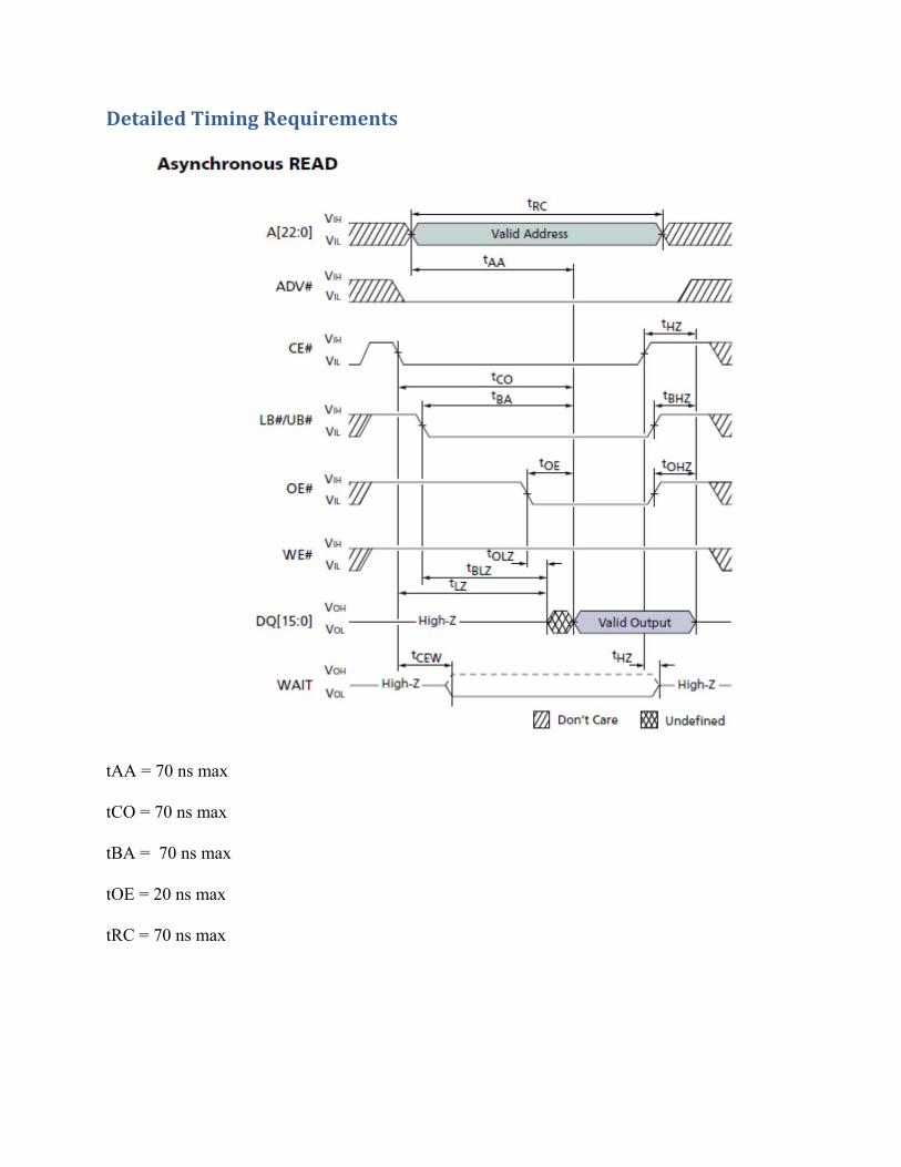
DetailedTimingRequirements
tAA = 70 ns max
tCO = 70 ns max
tBA = 70 ns max
tOE = 20 ns max
tRC = 70 ns max

Notes: 1. Low-Z to High-Z timings are tested with the circuit shown in Figure 27 on page 36. The
High-Z timings measure a 100mV transition from either VOH or VOL toward VCCQ/2. 2. igh-Z to Low-Z timings are tested with the circuit shown in Figure 27 on page 36. The Low-
Z timings measure a 100mV transition away from the High-Z (VCCQ/2) level toward eitherVOH or VOL.
3. Page mode enabled only.

tAW = 70 ns min tBW = 70 ns min tCW = 70 ns min tWP = 45 ns min tWHZ = 8 ns max
Note there are also figures for: LB#/UB#-Controlled Asynchronous WRITE WE#-Controlled Asynchronous WRITE

Notes: 1. Low-Z to High-Z timings are tested with the circuit shown in Figure 27 on page 36. The
High-Z timings measure a 100mV transition from either VOH or VOL toward VCCQ/2. 2. High-Z to Low-Z timings are tested with the circuit shown in Figure 27 on page 36. The
Low-Z timings measure a 100mV transition away from the High-Z (VCCQ/2) level toward either VOH or VOL.
3. WE# LOW time must be limited to tCEM (4μs).

As a final timing consideration there is a case of an write followed by read
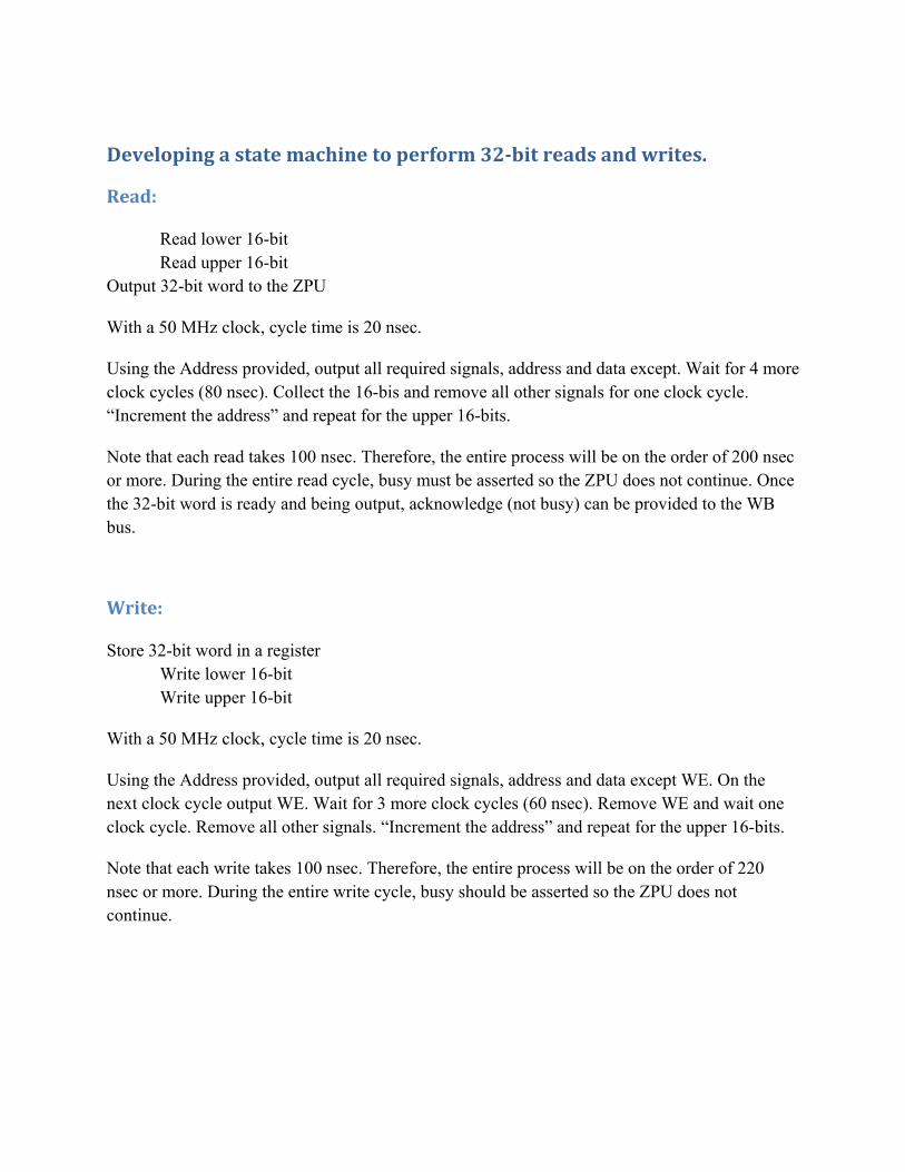
Developingastatemachinetoperform32‐bitreadsandwrites.
Read:
Read lower 16-bit Read upper 16-bit
Output 32-bit word to the ZPU
With a 50 MHz clock, cycle time is 20 nsec.
Using the Address provided, output all required signals, address and data except. Wait for 4 more clock cycles (80 nsec). Collect the 16-bis and remove all other signals for one clock cycle. “Increment the address” and repeat for the upper 16-bits.
Note that each read takes 100 nsec. Therefore, the entire process will be on the order of 200 nsec or more. During the entire read cycle, busy must be asserted so the ZPU does not continue. Once the 32-bit word is ready and being output, acknowledge (not busy) can be provided to the WB bus.
Write:
Store 32-bit word in a register Write lower 16-bit Write upper 16-bit
With a 50 MHz clock, cycle time is 20 nsec.
Using the Address provided, output all required signals, address and data except WE. On the next clock cycle output WE. Wait for 3 more clock cycles (60 nsec). Remove WE and wait one clock cycle. Remove all other signals. “Increment the address” and repeat for the upper 16-bits.
Note that each write takes 100 nsec. Therefore, the entire process will be on the order of 220 nsec or more. During the entire write cycle, busy should be asserted so the ZPU does not continue.
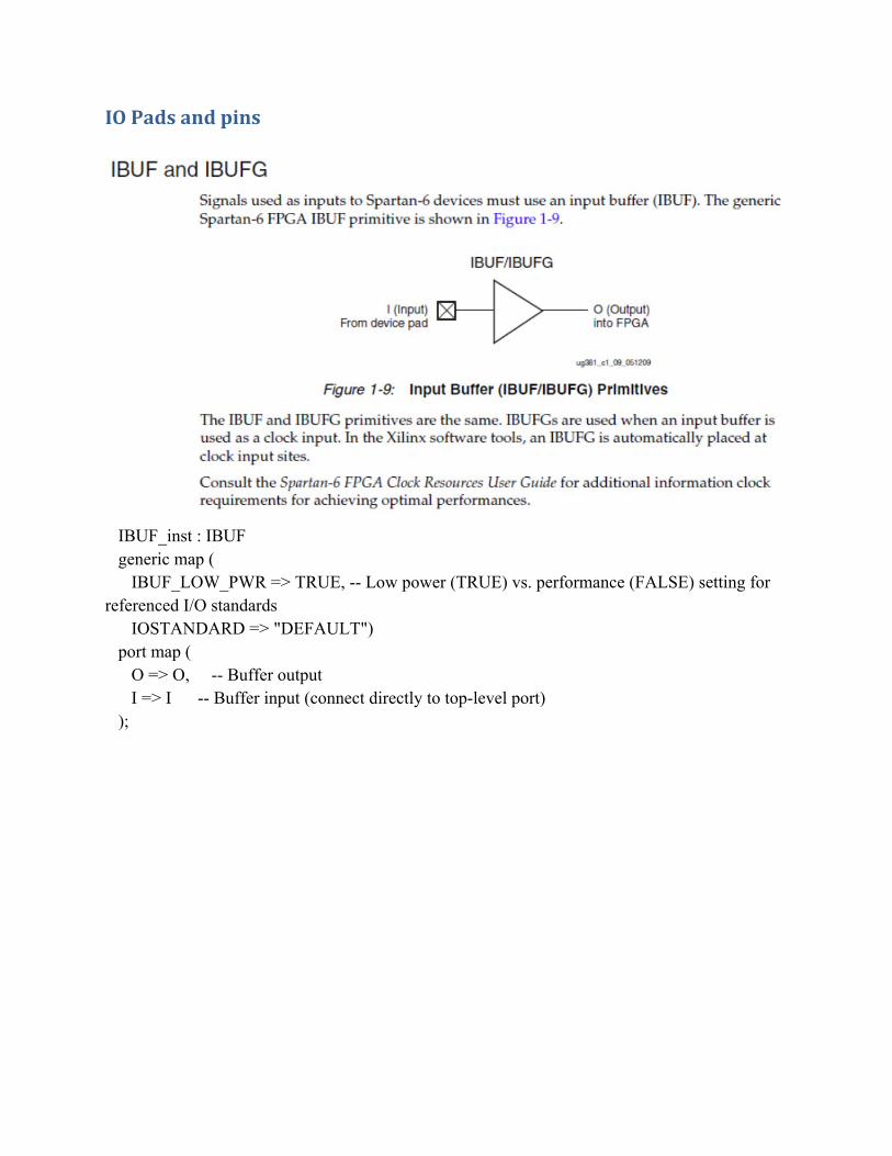
IOPadsandpins
IBUF_inst : IBUF generic map ( IBUF_LOW_PWR => TRUE, -- Low power (TRUE) vs. performance (FALSE) setting for referenced I/O standards IOSTANDARD => "DEFAULT") port map ( O => O, -- Buffer output I => I -- Buffer input (connect directly to top-level port) );
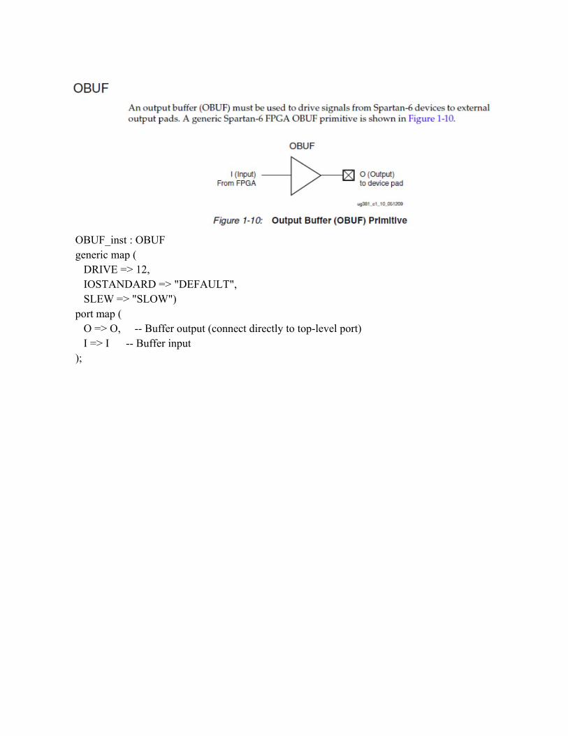
OBUF_inst : OBUF generic map ( DRIVE => 12, IOSTANDARD => "DEFAULT", SLEW => "SLOW") port map ( O => O, -- Buffer output (connect directly to top-level port) I => I -- Buffer input );
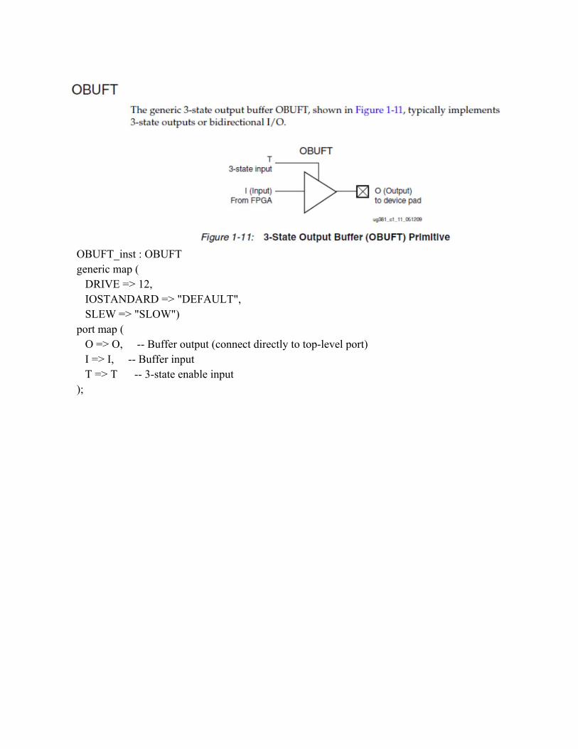
OBUFT_inst : OBUFT generic map ( DRIVE => 12, IOSTANDARD => "DEFAULT", SLEW => "SLOW") port map ( O => O, -- Buffer output (connect directly to top-level port) I => I, -- Buffer input T => T -- 3-state enable input );

IOBUF_inst : IOBUF generic map ( DRIVE => 12, IOSTANDARD => "DEFAULT", SLEW => "SLOW") port map ( O => O, -- Buffer output IO => IO, -- Buffer inout port (connect directly to top-level port) I => I, -- Buffer input T => T -- 3-state enable input, high=input, low=output ); From project2 and project4 PIO: gpio_in : in std_logic_vector(31 downto 0); gpio_out : out std_logic_vector(31 downto 0); gpio_dir : out std_logic_vector(31 downto 0) -- 1 = in, 0 = out Notices that the “data direction register” connects to T.

BehavioralBidirectionalPinMethodology
Port Definition at the Top level
MemAdr : out unsigned(CRAM_ADDR_W-1 downto 1);
MemDB : inout unsigned(MDATA_SIZE-1 downto 0)
Component Port Definitions
MemAdr_o : out unsigned(CRAM_ADDR_W-1 downto 1);
MemDB_i : in unsigned(MDATA_SIZE-1 downto 0);
MemDB_o : out unsigned(MDATA_SIZE-1 downto 0);
MemDB_dir : out std_logic
Signals used (redundant)
signal cram_idata : unsigned(MDATA_SIZE-1 downto 0);
signal cram_odata : unsigned(MDATA_SIZE-1 downto 0);
signal cram_ddr : std_logic;
VHDL Implementation
MemDB <= cram_odata when cram_ddr = '0' else "ZZZZZZZZZZZZZZZZ";
cram_idata <= MemDB;