cellulose nanofibril film as a piezoelectric sensor material 692, fi-33101 tampere, finland,...
TRANSCRIPT

Tampere University of Technology
Cellulose nanofibril film as a piezoelectric sensor material
CitationRajala, S., Siponkoski, T., Sarlin, E., Mettänen, M., Vuoriluoto, M., Pammo, A., ... Tuukkanen, S. (2016).Cellulose nanofibril film as a piezoelectric sensor material. ACS Applied Materials & Interfaces, 8(24),15607–15614. DOI: 10.1021/acsami.6b03597Year2016
VersionEarly version (pre-print)
Link to publicationTUTCRIS Portal (http://www.tut.fi/tutcris)
Published inACS Applied Materials & Interfaces
DOI10.1021/acsami.6b03597
CopyrightThis document is the unedited Author’s version of a Submitted Work that was subsequently accepted forpublication in ACS Applied Materials & Interfaces, copyright © American Chemical Society after peer review. Toaccess the final edited and published work see http://dx.doi.org/10.1021/acsami.6b03597.
Take down policyIf you believe that this document breaches copyright, please contact [email protected], and we will remove access tothe work immediately and investigate your claim.
Download date:20.06.2018

1
Satu Rajala1‡, Tuomo Siponkoski
2, Essi Sarlin
3, Marja Mettänen
1, Maija Vuoriluoto
4, Arno
Pammo1, Jari Juuti
2, Orlando J. Rojas
4, Sami Franssila
5 and Sampo Tuukkanen
1‡*
1 Department of Automation Science and Engineering, Tampere University of Technology, P.O.
Box 692, FI-33101 Tampere, Finland, [email protected], [email protected],
[email protected], [email protected],
2 Microelectronics Research Unit, Faculty of Information Technology and Electrical
Engineering, University of Oulu, P.O. Box 4500, FIN-90014 Oulu, Finland,
[email protected], [email protected]
3 Department of Materials Science, Tampere University of Technology, P.O. Box 692, FI-33101
Tampere, Finland, [email protected]
4 Department of Forest Products Technology, School of Chemical Technology, Aalto University,
P.O. Box 16300, FI-00076 Aalto, Finland, [email protected], [email protected]
5 Department of Materials Science and Engineering, School of Chemical Technology, Aalto
University, P.O. Box 11000, FI-00076 Aalto, Espoo, Finland, [email protected]
Cellulose nanofibril film as a piezoelectric
sensor material

2
Keywords: Cellulose nanofibrils; Piezoelectric sensors; Image based analysis; Sensitivity
measurement.
Abstract
Self-standing 45-µm-thick films of native cellulose nanofibrils (CNF) were synthesized and
characterized. The surface and the microstructure of the films were evaluated with image based
analysis and scanning electron microscopy (SEM). Dielectric properties of the films were
measured obtaining relative permittivity of 3.47 and 3.38 and loss tangent tan δ of 0.011 and
0.071 at 1 kHz and 9.97 GHz, respectively. The films were used as functional sensing layers in
piezoelectric sensors for which sensitivities from 4.7 to 6.4 pC/N were measured in ambient
conditions. This piezoelectric response is expected to increase remarkably after polarization of
crystalline cellulose regions in the film. The CNF sensor characteristics were evaluated and
compared with a reference piezoelectric polymer (polyvinylidenefluoride, PVDF). Overall, the
results suggest that nanocellulose is a suitable precursor for disposable piezoelectric sensors with
potential applications in fields of electronics, sensors and biomedical diagnostics.
1. Introduction
Cellulosic nanofibrils and nanocrystals1, referred to as nanocelluloses, are interesting
renewable bio-based nanomaterials with potential applications in different fields. The nanoscale
dimensions and strong ability to form entangled porous networks make nanocelluloses suitable
materials for fabrication of light-weight membranes, films, and nanopapers, all of which can be
3
processed in aqueous media. The use of solution-processable functional materials allows the low
cost and high throughput manufacturing of devices for electronics2,3, sensors4 or optics5.
Furthermore, when using nanocellulose in combination with solution-processable carbon based
nanomaterials, such as carbon nanotubes or graphene, flexible and disposable supercapacitors
can be prepared6–8.
The piezoelectricity of wood has been known for decades9,10. A classical definition of
piezoelectricity is the change of electrical polarization in a material in response to mechanical
stress11. This phenomenon is more pronounced in crystalline nanoscale materials, such as
cellulose nanocrystals (CNC)12,13. However, the topic has been covered in the scientific literature
to a very limited extent and only few recent studies report experimental evidence of CNC
piezoelectricity12,14. Herein, Frka-Petesic et al. reported recently about the experimental evidence
of giant permanent electric-dipole moment in cellulose nanocrystals14. Compared to CNC, the
higher aspect-ratio cellulose nanofibrils (CNF), containing both crystalline (cellulose I1) and
amorphous phases, can offer more versatile options as far as the synthesis of self-standing films
and nanopapers is profitable. Despite the principally randomly aligned crystalline regions in
CNF, their films are expected to show some level of piezoelectric behavior due to the film
fabrication process driven alignment. To our knowledge, piezoelectric measurements of CNF
films have not been attempted before the authors contribution15,16.
In this study, CNF films were fabricated and characterized through imaging, density and
dielectric measurements and electromechanical sensitivity measurements. The microstructure of
the films was studied using scanning electron microscopy (SEM). Also, the surface of the films

4
was evaluated through measurements based on optical images. The films were used as functional
materials in piezoelectric sensors and their sensitivity was measured by using a custom-built
setup. The sensors were excited with a shaker that delivered a sinusoidal input force and the
charge generated by the sensors was measured. The sensitivity is defined here as the charge
generated by the sensor divided by the force applied to excite the sensor. Finally, the sensor
characteristics including nonlinearity and hysteresis were measured and compared with a
reference piezoelectric polymer film (polyvinylidenefluoride, PVDF).
2. Materials and methods
2.1 Nanocellulose Piezoelectricity
The compression of a piezoelectric film by an external force causes charge separation in the
film generating a noticeable voltage between two electrodes. The piezoelectric coefficient dmn is
related to the charge density generated under a certain applied stress. A third-rank tensor of
piezoelectric coefficients dmn is expressed in terms of 3 × 6 matrix, where m = 1, 2, 3 refers to the
electrical axis and n = 1, 2, … , 6 to the mechanical axis11. The main axes 1, 2 and 3 correspond
to length, width and thickness, whereas the shear around these axes is represented by 4, 5 and 6.
The piezoelectric tensor dmn can be derived from the symmetry of a cellulose crystal lattice,
formed by unit cells of cellulose molecules ([C6H10O5]n)10. Cellulose belongs to a monoclinic
symmetry with space group of C2 || x3 having a following piezoelectric tensor:

5
=
36333231
2524
1514
00
0000
0000
dddd
dd
dd
dmn . (1)
This tensor is valid for a single cellulose crystal. However, for a film with randomly aligned
crystals (such as CNF film studied in this work), the overall piezoelectric response of the film is
a combination of different coefficients. For example, in the case of wood, arrangement of fibers
and accompanied cellulose crystals have been shown to exhibit greatly reduced effective
piezoelectric tensor:
=
000000
00000
00000
25
14
d
d
d mn , (2)
where d14 = -d25 9,10.
2.2. CNF film fabrication
Figure 1 describes schematically the deconstruction of nanocellulose from wood cellulose
fibers1. In this work, an industrial-grade bleached sulphite birch fibers suspended in water were
processed through a Masuko grinder using three consecutive passes and further homogenized
using six passes at 2000 bar pressure by using a M110P microfluidizer (Microfluidics Corp.,
Newton, MA, USA) equipped with 200 and 100 µm chambers. The resulting CNF material is
composed of crystalline (cellulose I1) and amorphous domains. When dispersed in the aqueous
medium, CNF was highly viscous and it can be classified as a hydrogel17. Films based on CNF
were fabricated by pressure filtering (15-30 min) followed by pressing and drying in a hot-press

6
at 100 °C for 2 h (described previously in more details18). An example of the resulting self-
standing CNF films is presented in the Figure 2a.
2.3. CNF film characterization
The CNF film was characterized by Scanning Electron Microscopy (SEM, Zeiss ULTRAplus).
Cross-sectional images were obtained by breaking the CNF film under liquid nitrogen and by
gluing the film to sample holders with conductive carbon cement. The samples were coated with
a thin carbon layer to provide electrical conductivity prior to the SEM imaging. Energy
Dispersive X-ray Spectroscopy (EDS, INCA Energy 350 with INCAx-act detector) was used to
ensure the purity of the CNF film. The apparent film density was calculated for a 5 cm x 8 cm
piece of CNF film by assuming an even film thickness obtained from the SEM analysis and mass
weighted by a microbalance.
The surface structure of the CNF film was also examined through photometric stereo imaging
and subsequent image analysis. Photometric stereo19 is a widely used technique in computer
graphics for surface analysis and reconstruction20, and it has also been successfully applied in
small-scale surface topography measurement, e.g., in paper industry21 and dermatology22. In
photometric stereo setup, the translucent CNF sample lied still on top of a flat black sheet of
cardboard while it was imaged with a camera from the top. Four images were taken from the
sample with different, but precisely known, illumination directions, using blue LEDs whose
dominant wavelength was 460 nm. The surface orientation (i.e., gradients) at each pixel was
estimated from the photographs; see Ref. 19 for details. The surface topography map was then
7
reconstructed from the gradient fields by integration23. The photographs were captured using a
digital systems camera (Canon EOS 550D) and a magnifying macro lens (Canon MP-E 65 mm).
With a slight magnification (1.3:1), a pixel size of 3.27 µm x 3.27 µm on an image area of
approximately 17 mm x 11 mm was achieved.
The dielectric properties of the CNF film were measured at 100 Hz to 1 MHz by using a LCR
meter (precision LCR meter 4284A, Keysight Technologies, USA). In order to increase
reliability of the measurement a stack of two films (total thickness of 96 µm) was measured
instead of a single 45 µm thick film. The sample was compressed gently between two external
electrodes of diameters 25 and 17.5 mm in a custom made measurement setup. The holder of
smaller electrode was made from soft rubber, covered with a conductive layer. This enabled the
sample to align better between the electrodes and improved applying of small pressures for the
sample to avoid deformation. To characterize dielectric properties also at higher frequencies, the
CNF film was measured at 9.97 GHz using a Split Post Dielectric Resonator (QWED, Warsaw,
Poland). This technique enables measurement without electrodes. Prior to both dielectric
measurements the films were hold 60 min at 100 °C to minimize the effect of air moisture in the
measurement results. Furthermore, a ferroelectric tester (Precision LC, Radiant technologies,
USA) was used to measure the ferroelectric hysteresis characteristics of the CNF film up to 50
V/µm electric field using 10 Hz frequency.
2.4. CNF and PVDF sensor assembly

8
Electrodes for the CNF sensors were fabricated on polyethylene terephthalate (PET, Melinex
ST506) substrate by e-beam evaporation (Varian vacuum evaporator). Electrodes were formed
by evaporating 100 nm thick copper (Cu) layer through a laser-cut stencil shadow mask.
The preparation of piezoelectric CNF sensors is described in Figure 2. Before the sensor
assembly, the CNF film shown in Figure 2a was cut into round shape pieces with a diameter
slightly larger than that of the electrodes, thus to avoid electrical breakdown over the edges. The
structure of the sensors is presented schematically in Figure 2b,c. The CNF pieces were then
sandwiched between two electrodes and fixed together from outside of the electrode perimeter
using a sticker film (2 way glue, manufactured by Kuretake Co.). A photograph of a fabricated
sensor is presented in Figure 2d. The total thickness of the assembled sensor was about 300 µm,
measured with a micrometer screw.
In total, four CNF sensors with electrode diameter of 15 mm were assembled and measured in
this work. In addition, one larger CNF sensor (with electrode diameter of 20 mm) was fabricated
and compared to a reference polyvinylidenefluoride (PVDF) sensor, assembled with the same
method as the CNF sensors. A larger electrode area was used to study the sensitivity distribution
over the sensor surface. PVDF is a piezoelectric polymer material that is widely used in versatile
sensor applications, and thus, it was chosen here as a reference. For instance, the PVDF material
is used in mechanical (e.g. pressure, acceleration, vibration and tactile sensors etc.), acoustics
and IR sensors24. Application areas also include energy conversion25 and medical
measurements26–28. An unmetallized, 28 µm thick PVDF film manufactured by Measurement
Specialties Inc. (Hampton, USA) was used in this study29.
9
2.5. Piezoelectric sensitivity measurements
A Brüel & Kjaer Mini-Shaker Type 4810 generating a dynamic excitation force was used in
the sensor sensitivity measurements. A sinusoidal input for the shaker was provided with a
Tektronix AFG3101 function generator. A commercial high sensitivity dynamic force sensor
(PCB Piezotronics, model 209C02) was used as a reference sensor for the dynamic excitation
force. A load cell (Measurement Specialties Inc., model ELFS-T3E-20L) was used as reference
sensor to measure the static force between the sample and shaker’s piston (diameter 4 mm). A
pre-compression, which produces the static force, is needed to keep the sample in place and to
prevent the piston from jumping off the surface during the measurement. Figure 3 shows in detail
the sensor sensitivity measurement setup. The same measurement principle has been previously
used to evaluate the sensor sensitivity of piezoelectric polymer film (PVDF)26–28,30–33.
The sensor sensitivity measured in this study is closely related to the longitudinal piezoelectric
coefficient d33. The longitudinal d33 coefficient describes the electric polarization generated in
the same direction as the stress is applied34. Thus, in the measurement of the sensor sensitivity,
the electrodes were located on the top and the bottom of the sensor material and the film was
excited with a dynamic force in the Z or thickness direction. The sensitivity is defined here as the
charge generated by the sensor divided by the normal force used to excite the sensor. The unit of
sensitivity is thus C/N.
10
To measure the sensor sensitivity of the four CNF sensors (diameter 15 mm) in the thickness
direction, the sensor was placed horizontally on the metal plate, see Figure 3. The charge
developed by the sensor was measured with a custom-made combination of a charge amplifier
and a 16-bit AD-converter. The connection to the AD-converter from the sensor was provided
via coaxial wires and crimp connectors (Nicomatic Crimpflex). The AD-converter also had
additional channels for sampling the voltage signals from the reference sensors. The measured
data was processed to solve the sensitivity of the sensor to the force. Since the excitation force
was sinusoidal, the sensitivity was calculated simply by dividing the amplitudes of the respective
signals. Possible baseline drift in the signals was removed with high-pass filtering before the
sinusoidal amplitudes were solved by fitting sinusoidal waveforms to the signals as described in
the IEEE Standard for Digitizing Waveform Recorders (IEEE Std 1241).
A static force of approximately 3 N was applied. The sensor was excited with sinusoidal 2 Hz
input signal of an approximate force of 1.4 N (peak-to-peak). The excitation was applied in the
middle of the sensor. The measurement was repeated three times; between the measurements the
static force was relieved and the sensor was re-positioned on the metal plate for a new
measurement. The same measurements were conducted from both sides of the sensor, resulting
in a total of six excitation rounds per sensor.
2.6. Measurement of sensor characteristics
In addition to the piezoelectric sensitivity measurements described in the previous Section,
more comprehensive measurements were performed on the CNF sensor with the electrode

11
diameter of 20 mm. The similar measurements were also carried out with the reference PVDF
sensor. First, the sensitivity distribution over the sensor surface was measured. The CNF and
PVDF sensors were excited by applying force to nine different locations on the sensor area, one
at a time (see Figure 8a). The same positions were excited from both sides of the sensor,
resulting in a total of 18 excitation rounds per sensor.
Next, the charge developed by the CNF and PVDF sensors was measured as a function of
dynamic excitation force to determine the nonlinearity of the sensor. The amplitude of the
dynamic excitation force was altered from approximately 0.1 N to 5 N (peak-to-peak) with a
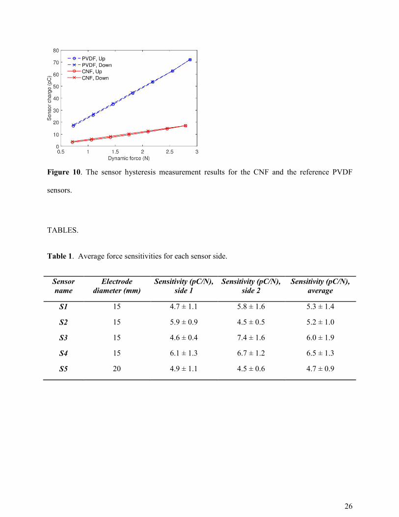
frequency of 2 Hz. Finally, the hysteresis error for the sensors was determined. The sensor
hysteresis error is defined as the deviation of the sensor’s output at a specified point of the input
signal when this point is approached from opposite directions35. Here the sensor hysteresis curve
was determined by measuring the generated charge as a function of dynamic excitation force,
first by increasing the force between the excitation rounds (duration about 10 seconds) and then
by decreasing it. At each excitation round, no fatigue in sensor signals was observed during the
excitation. The excitation force range was approximately 0.7-2.8 N (peak-to-peak) with a
frequency of 2 Hz.
3. Results
3.1. CNF film characterization

12
Cross-sectional and plane view micrographs (SEM) of a CNF film are shown in Figure 4. The
cross-section of the film (Figure 4a) reveals a layered, porous structure with an average thickness
of 45 ± 3 µm. The film structure is similar to those obtained in a previous study18. The surface
view of the film (Figure 4b) shows the random orientation of nanofibrils. No traces of defects or
possible contaminants were found. The density of the CNF film was estimated to be 1.38 g/cm3,
based on measurement of film dimensions and weight measured in ambient air.
The photometric stereo images and the reconstructed surface topography map reveal a
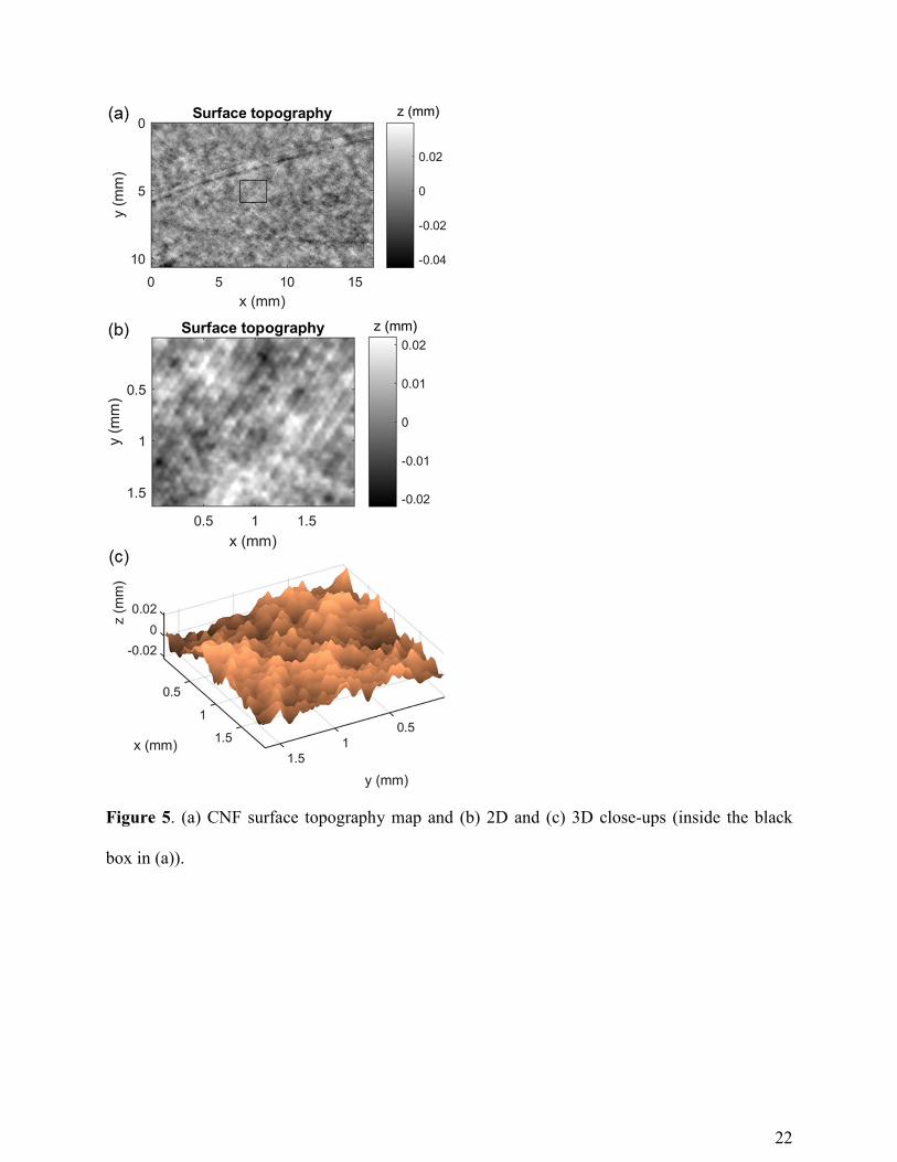
prominent streaky structure on the surface of the CNF film. Figure 5a illustrates the surface
topography map, showing the typical cloudy and random appearance of webs formed from fiber
suspensions. The close-up (Figure 5b,c) clearly shows the streaky pattern, presumably produced
by the filter mesh on top of which the CNF film was fabricated. The distance between the
diagonal streaks on the surface is approximately 140 µm, and the finer regular structure seen on
each streak corresponds to the distances between the wires of the mesh, approximately 48 µm.
The streaky pattern is clearly visible on both sides of the CNF film. 2D spectrum analysis of the
photometric stereo based surface topography from an area of several square millimeters also
confirmed the SEM-based finding that the cellulose constituents in the film are randomly
oriented in the plane of the film.
The calculated relative permittivity and dielectric loss tangent values for the CNF film
obtained from the LCR measurements are presented as a function of measurement frequency in
Figure 6. The error bars show the approximated 2 % error for capacitance values in
measurements. Obtained relative permittivity of CNF film was about 3.47 and dielectric loss (tan

13
δ) about 0.011 at a 1 kHz frequency. The capacitance of CNF film varied from 78 pF to 73 pF at
100 Hz to 1 MHz, respectively. The average relative permittivity and dielectric losses were 3.38
and 0.071, respectively, measured with SPDR with nominal frequency of 9.97 GHz.
The results of ferroelectric hysteresis measurements are shown in the Figure 7. The
capacitance or linear component in the polarization data is dominant in the measurements at
electric fields from 5 to 15 V/µm, thus showing that CNF film has no significant ferroelectric
hysteresis at low or moderate electric fields (Figure 7a). However, between 40 to 50 V/µm
electric fields (Figure 7b) nonlinear behavior is detected. This suggests that the film has some
level of ferroelectric properties at high electric fields, but remanent polarization at 50 V/µm field
is still small (0.15 µC/cm²).
3.2. Sensor sensitivity and characteristics
The operation of four nominally identical CNF sensors with diameter of 15 mm was evaluated
with sensitivity measurements (Table 1). The values are presented as mean sensitivities ±
standard deviations for each sensor side. The average sensitivity value for the four CNF sensors
was (5.7 ± 1.2) pC/N.
The more thorough sensor characteristics measurements were performed for one CNF sensor
and one PVDF reference. Figure 8a shows the excitation positions for the sensor sensitivity
distribution measurement. Both sensor samples had electrodes of 20 mm in diameter while the
shaker’s piston was 4 mm in diameter, as illustrated in Figure 8a. In Figure 8b, the CNF and

14
PVDF sensor sensitivities as a function of the excitation position are shown. The sensitivity over
the sensor the surface was found to be almost constant. The average sensitivity for the CNF
sensor was found to be 4.7 ± 0.9 pC/N, while that of the reference PVDF sensor was 27.5 ± 2.6
pC/N.
The nonlinearity is defined as the maximum deviation of a real transfer function from a linear
correlation35. Here the nonlinearity was determined by fitting a first degree polynomial via least-
squares minimization (Matlab function polyfit). Figure 9 shows the charge generated by the CNF
and PVDF sensors as a function of the dynamic excitation force. The fitted polynomials for the
sensors are shown with a blue dashed line (PVDF 34.01x-9.66) and red solid line (CNF 6.51x-
1.23). Instead of the maximum deviation from the linear correlation, the nonlinearity is presented
here as the mean ± standard deviation of data point deviations from the fitted polynomial. For the
reference PVDF sensor the nonlinearity was found to be 6.47 ± 3.76 pC and for the CNF sensor
0.86 ± 0.48 pC.
Figure 10 shows the sensor hysteresis measurement results. The measurements made by
increasing the dynamic excitation force are marked with solid line and circles and the
measurements made by decreasing the force with dashed line and crosses. For the reference
PVDF sensor the maximum difference between the increasing and decreasing measurements was
0.93 pC and for the CNF sensor 0.92 pC.
4. Discussion

15
The cellulose nanofibril (CNF) films were fabricated and characterized through SEM imaging,
measurements based on optical images and density measurements. The SEM images revealed a
layered, porous structure. The structure of the CNF film resembles the structure of an electret
material, ElectroMechanical Film (EMFi), used in sensor applications36,37. The surface
topography of the CNF film is dominated by streaks, approximately 140 µm apart from each
other, apparently reproduced from the formation fabric mesh18. Apart from the mesh-induced
pattern, the surface of the film is fairly smooth and the fibrous structure has random orientation.
The density of the CNF film was found to be 1.38 g/cm3 which is similar to earlier study where
similar films were prepared18. In comparison, the densities of the PVDF and EMFi sensor
materials are 1.78 g/cm3 29 and 0.33 g/cm3 36, respectively. Since the CNF film has a porous
structure, it is reasonable that the density of the CNF film is slightly lower that of the PVDF film.
On the other hand, the EMFi film has much lower density due to the gas filled voids separated by
polypropylene layers, formed during the film manufacturing process.
The CNF film permittivity was obtained from both LCR and resonator measurements and they
match very well, giving a relative permittivity of about 3.4. This is close to values of dielectric
polymers such as polyimide and polytetrafluoroethylene in general and since organic materials
are known to have low relative permittivity, the results are considered to be reasonable38. The
change in relative permittivity as a function of frequency was clearly seen from the LCR
measurement. At the same time, dielectric losses are increasing rapidly from 10 kHz onward
accompanied with steeper declining of relative permittivity which is typical indication of
relaxation mechanism taking place (Figure 6). However, the change of relative permittivity was
quite small, around 7 % from 100 Hz to 1 MHz, and it was at similar level as obtained at ~10

16
GHz, suggesting that only minor level of dielectric relaxation phenomena is occurring due
Maxwell-Wagner-Sillars (MWS) type of the polarization39. Such polarization takes place
typically at acoustic frequencies and is associated with e.g. immobilized free charges on the
interfaces of different media having contrast in conductivity and permittivity. In the case of
EMFi, charges are designedly introduced into the gas filled voids separated by polypropylene
layers while in this case they can be byproduct of the manufacturing process, yet having
effectively similar function as in EMFi. Since the sensor sensitivity measurement was carried out
at low frequencies, possible influence of MWS polarization cannot be excluded at this point.
Therefore, actual mechanism behind the measured results remains still unclear, and is out of
scope of this paper, but can be concluded utilizing e.g. higher frequency measurements as the
dielectric relaxation expands over wider frequency spectrum than MWS relaxation.
In addition, it should be pointed out that the used external electrodes pushed against the
surfaces of the sample may cause errors in dielectric and ferroelectric measurements. Any
porosity between the electrodes and the sample in general decreases the coupling of the electric
field and measured capacitance. The surface contact is also making it difficult to distinguish
which losses are from material or due to contact. Therefore, using of two different dielectric
measurements, with and without electrodes, reasonable conclusions could be drawn to avoid
misinterpretation.
In the ferroelectric hysteresis measurement it was noticed that CNF film can withstand quite
high electric fields even though it has porous microstructure. Small ferroelectric effect could be
found with electric field above ~40 V/µm. It is commonly known that organic ferroelectric

17
materials have usually much higher coercive field than similar inorganic materials40. It should be
noted that the above mentioned issue with electrode contacts may hinder also ferroelectric
results. With respect to the obtained results it seems that nanocellulose is acting like incipient
organic ferroelectric material when very high electric field is present40. In such case the observed
piezoelectric effect in CNF is then resulting from the permanent dipole moment of CNCs with
some level of orientation due to the fabrication process of the film in contrast to earlier
mentioned observations with individual CNC crystals12,14.
The piezoelectric sensors were fabricated from the 45 µm-thick CNF film and copper
electrodes evaporated on a PET substrate. The sensitivity of the fabricated sensors was measured
using a dedicated measurement setup. All five (four of 15 mm and one of 20 mm electrode
diameter) prepared piezoelectric CNF sensors showed similar sensor sensitivity values, with
sensitivity averages from 4.7 to 6.4 pC/N. These results suggest that the nanofibrils are
homogeneously distributed inside the film and the sensitivity values are reliable. Both the CNF
sensor and the PVDF reference sensor were found to be rather linear inside the used
measurement range. The sensor hysteresis of the CNF sensors was found to be larger than that of
the PVDF sensor. However, the hysteresis was negligible for both types of sensors.
In 2000 Fukada concluded, that a shear piezoelectric coefficient d14 for wood cellulose is as
low as -0.1 pC/N41, which does not suggest high applicability of cellulose as piezoelectric sensor
material. However, the case is different with the extracted nanocrystals and nanofibrils. There are
recent experimental evidences that the orientation of CNC crystals has a significant effect on the
overall piezoelectric response12, and that CNC has a permanent dipole momentum14. It was also

18
suggested that regenerated CNC (cellulose II) has the apparent piezoelectric coefficient on the
range 35-60 pC/N13. One should point out that the CNF film studied in this work was not
optimized as a piezoelectric material and was not polarized or oriented purposely. However, the
CNF film fabrication method, such as filtering and hot-pressing, may have caused some
alignment of the cellulose nanofibrils inside the thick film. The sensor sensitivity obtained for
the CNF film in this work is expected to significantly increase by intentional material design
aiming at optimal alignment of CNC dipoles. The poling procedure, in general, consists of
applying an electric field on a processed film for a certain period of time in order to generate
piezoelectric properties. The poling (or other type orientation) of the CNF film should lead to the
polarization of the crystalline CNC regions inside the CNF film, further leading to a remarkable
increase of piezoelectric effect due to the large piezoelectric coefficient of the crystalline
components12,14. In comparison, a sensitivity of about 27.5 pC/N was obtained here for a sensor
made from a polarized 28-µm-thick PVDF film29. This is about four times larger than the sensor
sensitivity of the CNF film measured in this work. The initial results of orientation of water-
processed CNF-films, using DC voltage, suggest the potential of remarkably higher sensitivity
values16. However, polarization of dry film is difficult due to the entangled and stiff structure of
the film and thus, further fabrication process development is required in order to increase the
CNF film sensitivity.
The sensor structure composing of the CNF films sandwiched between the copper electrodes
on PET may affect the measured sensitivity values: the contact between the actual sensing
material and the electrode is not as good as in the case of electrodes processed directly on the

19
sensing material. In comparison, less variation in sensitivity values were observed when
electrodes were either printed or evaporated directly on PVDF film32,33.
To conclude, functional piezoelectric sensor elements were fabricated from CNF film and
subsequently their piezoelectric sensitivity was measured. Also, a principal material
characterization for CNF film was done using optical and dielectric, ferroelectric and
electromechanical measurements. The obtained results in this study suggest that nanocellulose
film is a suitable sensor material for applications in fields such as sensors, electronics and
biomedical diagnostics.
FIGURES
Figure 1. Schematic view of nanocellulose fabrication from wood cellulose fibers. The cellulose
fibers are first deconstructed into microfibrils and after various processing steps into cellulose

20
nanofibrils (CNF). Cellulose nanocrystals (CNC) can be further obtained by using acid
hydrolysis. For more details see reference1.
Figure 2. (a) A photograph of the fabricated self-standing CNF film. An insert image presents
the bending robustness of the film. (b,c) A schematic side-view of the piezoelectric sensor
structure, (d) a photograph of assembled sensor.
Figure 3. The sensor sensitivity measurement setup.

21
Figure 4. (a) Cross-section and (b) plane view images (SEM) of a CNF film.
22
Figure 5. (a) CNF surface topography map and (b) 2D and (c) 3D close-ups (inside the black
box in (a)).

23
Figure 6. Relative permittivity and loss tangent (tan δ) of CNF film obtained from LCR
measurements.

24
Figure 7. The polarization-voltage hysteresis measurement of CNF (a) at 5-15 V/µm and (b) 40-
50 V/µm electric fields at room temperature.
25
Figure 8. (a) The excitation positions for the sensitivity distribution measurements and (b) the
sensor sensitivities as a function of excitation position.
Figure 9. The sensor nonlinearity measurement results for the CNF and reference PVDF sensors.
26
Figure 10. The sensor hysteresis measurement results for the CNF and the reference PVDF
sensors.
TABLES.
Table 1. Average force sensitivities for each sensor side.
Sensor
name
Electrode
diameter (mm)
Sensitivity (pC/N),
side 1
Sensitivity (pC/N),
side 2
Sensitivity (pC/N),
average
S1 15 4.7 ± 1.1 5.8 ± 1.6 5.3 ± 1.4
S2 15 5.9 ± 0.9 4.5 ± 0.5 5.2 ± 1.0
S3 15 4.6 ± 0.4 7.4 ± 1.6 6.0 ± 1.9
S4 15 6.1 ± 1.3 6.7 ± 1.2 6.5 ± 1.3
S5 20 4.9 ± 1.1 4.5 ± 0.6 4.7 ± 0.9

27
AUTHOR INFORMATION
Corresponding Author
*Phone: +358 40 541 5276, Email: [email protected].
Author Contributions
MV has prepared the CNF films. MM has performed the image based analysis for the CNF films.
ES has performed the scanning electron microscopy analysis. AP and ST have fabricated the
piezoelectric sensors. SR has performed the piezoelectric sensitivity measurements and analyzed
the results with ST. TS have performed the dielectric properties and ferroelectric hysteresis
measurements and analyzed the results with JJ. SR and ST wrote the most of the manuscript. All
authors commented the manuscript and gave their approval to the final version of the manuscript.
‡These authors contributed equally.
Notes
The authors declare no competing financial interest.
ACKNOWLEDGMENT
The authors acknowledge funding from the Academy of Finland (Dec. No. 137669, 258124
and 264743).
REFERENCES
(1) Moon, R. J.; Martini, A.; Nairn, J.; Simonsen, J.; Youngblood, J. Cellulose Nanomaterials
Review: Structure, Properties and Nanocomposites. Chem. Soc. Rev. 2011, 40 (7), 3941.
(2) Vuorinen, T.; Zakrzewski, M.; Rajala, S.; Lupo, D.; Vanhala, J.; Palovuori, K.;

28
Tuukkanen, S. Printable, Transparent, and Flexible Touch Panels Working in Sunlight and
Moist Environments. Adv. Funct. Mater. 2014, 24 (40), 6340–6347.
(3) Lehtimäki, S.; Tuukkanen, S.; Pörhönen, J.; Moilanen, P.; Virtanen, J.; Honkanen, M.;
Lupo, D. Low-Cost, Solution Processable Carbon Nanotube Supercapacitors and Their
Characterization. Appl. Phys. A 2014, 117 (3), 1329–1334.
(4) Rim, Y. S.; Bae, S.-H.; Chen, H.; De Marco, N.; Yang, Y. Recent Progress in Materials
and Devices toward Printable and Flexible Sensors. Adv. Mater. 2016.
(5) Isoniemi, T.; Tuukkanen, S.; Cameron, D. C.; Simonen, J.; Toppari, J. J. Measuring
Optical Anisotropy in poly(3,4-Ethylene Dioxythiophene):poly(styrene Sulfonate) Films
with Added Graphene. Org. Electron. 2015, 25, 317–323.
(6) Tuukkanen, S.; Lehtimaki, S.; Jahangir, F.; Eskelinen, A.-P.; Lupo, D.; Franssila, S.
Printable and Disposable Supercapacitor from Nanocellulose and Carbon Nanotubes. In
Proceedings of the 5th Electronics System-integration Technology Conference (ESTC);
IEEE, 2014; pp 1–6.
(7) Torvinen, K.; Lehtimäki, S.; Keränen, J. T.; Sievänen, J.; Vartiainen, J.; Hellén, E.; Lupo,
D.; Tuukkanen, S. Pigment-Cellulose Nanofibril Composite and Its Application as a
Separator-Substrate in Printed Supercapacitors. Electron. Mater. Lett. 2015, 11 (6), 1040–
1047.
(8) Lehtimäki, S.; Suominen, M.; Damlin, P.; Tuukkanen, S.; Kvarnström, C.; Lupo, D.
Preparation of Supercapacitors on Flexible Substrates with Electrodeposited
PEDOT/Graphene Composites. ACS Appl. Mater. Interfaces 2015, 7 (40), 22137–22147.

29
(9) Fukada, E. Piezoelectricity of Wood. J. Phys. Soc. Japan 1955, 10 (2), 149–154.
(10) Fukada, E. Piezoelectricity as a Fundamental Property of Wood. Wood Sci. Technol. 1968,
2 (4), 299–307.
(11) Harrison, J. S.; Ounaies, Z. Piezoelectric Polymers. In Encyclopedia of Polymer Science
and Technology; John Wiley & Sons, Inc.: Hoboken, NJ, USA, 2002; Vol. 3.
(12) Csoka, L.; Hoeger, I. C.; Rojas, O. J.; Peszlen, I.; Pawlak, J. J.; Peralta, P. N. Piezoelectric
Effect of Cellulose Nanocrystals Thin Films. ACS Macro Lett. 2012, 1 (7), 867–870.
(13) Cheng, H. FlexoElectric Nanobiopolymers (FEPs) Exhibiting Higher Mechanical Strength
(7.5 GPa), Modulus (250 GPa), and Energy Transfer Efficiency (75%). Worldw.
Electroact. Polym. (Artificial Muscles) Newsl. 2008, 10 (2), 5–7.
(14) Frka-Petesic, B.; Jean, B.; Heux, L. First Experimental Evidence of a Giant Permanent
Electric-Dipole Moment in Cellulose Nanocrystals. EPL (Europhysics Lett. 2014, 107 (2),
28006.
(15) Rajala, S.; Vuoriluoto, M.; Rojas, O. J.; Franssila, S.; Tuukkanen, S. Piezoelectric
Sensitivity Measurements of Cellulose Nanofibril Sensors. In Proc. XXI IMEKO World
Congr.; Prague, Czech Republic, 2015; pp 2–6.
(16) Tuukkanen, S.; Rajala, S. A Survey of Printable Piezoelectric Sensors. In Proc. IEEE
SENSORS Conference; IEEE: Busan, South Korea, 2015; pp 1–4.
(17) Pääkko, M.; Ankerfors, M.; Kosonen, H.; Nykänen, a.; Ahola, S.; Österberg, M.;
Ruokolainen, J.; Laine, J.; Larsson, P. T.; Ikkala, O.; Lindström, T. Enzymatic Hydrolysis
Combined with Mechanical Shearing and High-Pressure Homogenization for Nanoscale

30
Cellulose Fibrils and Strong Gels. Biomacromolecules 2007, 8 (6), 1934–1941.
(18) Österberg, M.; Vartiainen, J.; Lucenius, J.; Hippi, U.; Seppälä, J.; Serimaa, R.; Laine, J. A
Fast Method to Produce Strong NFC Films as a Platform for Barrier and Functional
Materials. ACS Appl. Mater. Interfaces 2013, 5 (11), 4640–4647.
(19) Woodham, R. J. Photometric Method for Detemining Surface Orientation from Multiple
Images. Opt. Eng. 1980, 19 (1), 139–144.
(20) Goldman, D. B.; Curless, B.; Hertzmann, A.; Seitz, S. M. Shape and Spatially-Varying
BRDFs from Photometric Stereo. IEEE Trans. Pattern Anal. Mach. Intell. 2010, 32 (6),
1060–1071.
(21) Mettänen, M. Measurement of Print Quality: Joint Statistical Analysis of Paper
Topography and Print Defects, Tampere University of Technology, 2010.
(22) Sohaib, A.; Farooq, A. R.; Atkinson, G. a; Smith, L. N.; Smith, M. L.; Warr, R. In Vivo
Measurement of Skin Microrelief Using Photometric Stereo in the Presence of
Interreflections. J. Opt. Soc. Am. A. Opt. Image Sci. Vis. 2013, 30 (3), 278–286.
(23) Frankot, R. T.; Chellappa, R. Method for Enforcing Integrability in Shape From Shading
Algorithms. IEEE Trans. Pattern Anal. Mach. Intell. 1988, 10 (4), 439–451.
(24) Harsányi, G. Polymer Films in Sensor Applications: A Review of Present Uses and Future
Possibilities. Sens. Rev. 2000, 20 (2), 98–105.
(25) Lang, S. B.; Muensit, S. Review of Some Lesser-Known Applications of Piezoelectric and
Pyroelectric Polymers. Appl. Phys. A Mater. Sci. Process. 2006, 85 (2), 125–134.

31
(26) Rajala, S.; Lekkala, J. Film-Type Sensor Materials PVDF and EMFi in Measurement of
Cardiorespiratory Signals a Review. IEEE Sens. J. 2012, 12 (3), 439–446.
(27) Tuukkanen, S.; Julin, T.; Rantanen, V.; Zakrzewski, M.; Moilanen, P.; Lilja, K. E.; Rajala,
S. Solution-Processible Electrode Materials for a Heat-Sensitive Piezoelectric Thin-Film
Sensor. Synth. Met. 2012, 162 (21-22), 1987–1995.
(28) Kärki, S.; Lekkala, J.; Kuokkanen, H.; Halttunen, J. Development of a Piezoelectric
Polymer Film Sensor for Plantar Normal and Shear Stress Measurements. Sensors
Actuators, A Phys. 2009, 154 (1), 57–64.
(29) Measurement Specialties Inc. Piezo film sensors, Technical manual http://www.meas-
spec.com (accessed May 5, 2014).
(30) S. Kärki, M. Kiiski, M. Mäntysalo, J. L. A PVDF Sensor with Printed Electrodes for
Normal and Shear Stress Measurements on Sole. In Proc. XIX IMEKO World Congr.;
Lisbon, Portugal, 2009; pp 1765–1769.
(31) Tuukkanen, S.; Julin, T.; Rantanen, V.; Zakrzewski, M.; Moilanen, P.; Lupo, D. Low-
Temperature Solution Processable Electrodes for Piezoelectric Sensors Applications. Jpn.
J. Appl. Phys. 2013, 52 (5S1), 05DA06.
(32) Rajala, S. N. K.; Mettanen, M.; Tuukkanen, S. Structural and Electrical Characterization
of Solution-Processed Electrodes for Piezoelectric Polymer Film Sensors. IEEE Sens. J.
2016, 16 (6), 1692–1699.
(33) Rajala, S.; Tuukkanen, S.; Halttunen, J. Characteristics of Piezoelectric Polymer Film
Sensors With Solution-Processable Graphene-Based Electrode Materials. IEEE Sens. J.
32
2015, 15 (6), 3102–3109.
(34) Ramadan, K. S.; Sameoto, D.; Evoy, S. A Review of Piezoelectric Polymers as Functional
Materials for Electromechanical Transducers. Smart Mater. Struct. 2014, 23 (3), 033001.
(35) Fraden, J. Handbook of Modern Sensors: Physics, Designs, and Applications, 2nd Ed.;
2010.
(36) Paajanen, M.; Lekkala, J.; Kirjavainen, K. ElectroMechanical Film (EMFi) — a New
Multipurpose Electret Material. Sensors Actuators A Phys. 2000, 84 (1-2), 95–102.
(37) Barna, L., Koivuluoma, M., Hasu, M., Tuppurainen, J. and Värri, A. The Use of
Electromechanical Film (EMFi) Sensors in Building a Robust Touch-Sensitive Tablet-like
Interface. IEEE Sens. J. 2007, 7 (1), 74–80.
(38) DuPont, DuPont Kapton FPC Polyimide Film, Technical Data Sheet
http://www.dupont.com/content/dam/dupont/products-and-services/membranes-and-
films/polyimde-films/documents/DEC-Kapton-FPC-datasheet.pdf (accessed Mar 2, 2016).
(39) Perrier, G.; Bergeret, A. Polystyrene-Glass Bead Composites: Maxwell-Wagner-Sillars
Relaxations and Percolation. J. Polym. Sci. Part B Polym. Phys. 1997, 35 (9), 1349–1359.
(40) Horiuchi, S.; Tokura, Y. Organic Ferroelectrics. Nat. Mater. 2008, 7 (5), 357–366.
(41) Fukada, E. History and Recent Progress in Piezoelectric Polymers. IEEE Trans. Ultrason.
Ferroelectr. Freq. Control 2000, 47 (6), 1277–1290.