ceng 4480 l08 memory 2byu/ceng4480/2016fall/l08_memory2.pdf · ceng4480 l08. memory-2 storage based...
TRANSCRIPT
1
Reference:• Chapter 11 Memories• CMOS VLSI Design—A Circuits and Systems Perspective
• by H.E.Weste and D.M.Harris
CENG 4480L08 Memory 2
Bei Yu
L08. Memory-2CENG4480
CENG4480 v.s. CENG3420
• CENG3420:✦ architecture perspective✦ memory coherent✦ data address
• CENG4480: more details on how data is stored
2
L08. Memory-2CENG4480
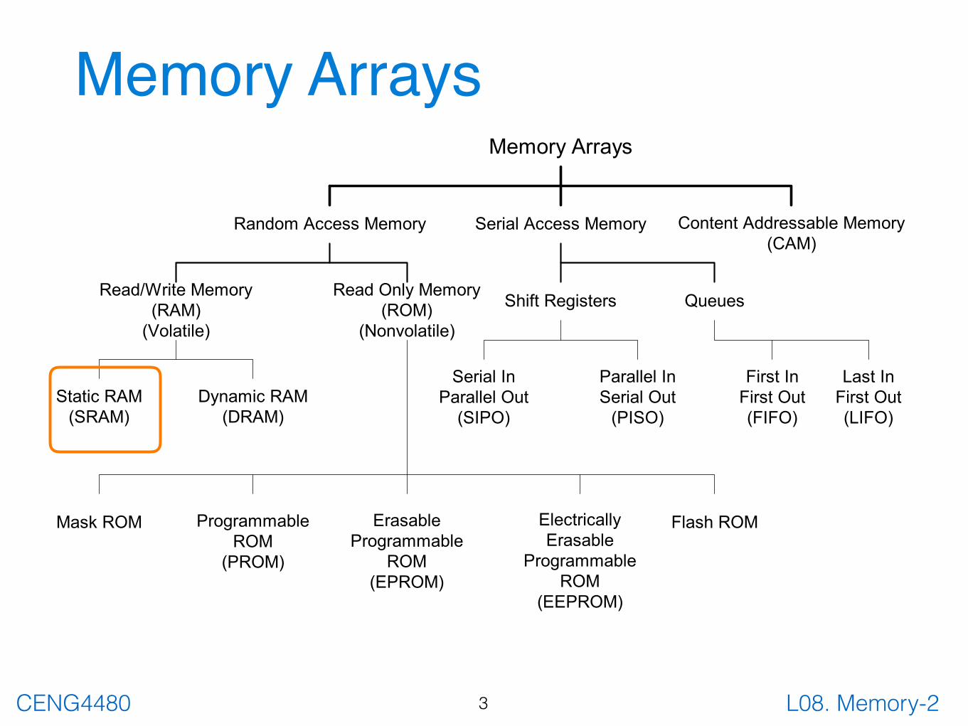
Memory Arrays
Random Access Memory Serial Access Memory Content Addressable Memory(CAM)
Read/Write Memory(RAM)
(Volatile)
Read Only Memory(ROM)
(Nonvolatile)
Static RAM(SRAM)
Dynamic RAM(DRAM)
Shift Registers Queues
First InFirst Out(FIFO)
Last InFirst Out(LIFO)
Serial InParallel Out
(SIPO)
Parallel InSerial Out
(PISO)
Mask ROM ProgrammableROM
(PROM)
ErasableProgrammable
ROM(EPROM)
ElectricallyErasable
ProgrammableROM
(EEPROM)
Flash ROM
Memory Arrays
3

L08. Memory-2CENG4480
Storage based on Feedback• What if we add feedback to a pair of inverters?
• Usually drawn as a ring of cross-coupled inverters
• Stable way to store one bit of information (w. power)
4
0 01
1
1 0
0

L08. Memory-2CENG4480
How to change the value stored?• Replace inverter with NAND gate
• RS Latch
5
A B A nand B0 0 10 1 11 0 11 1 0
S
R
Q
Q̄
1
1 0
0
L08. Memory-2CENG4480
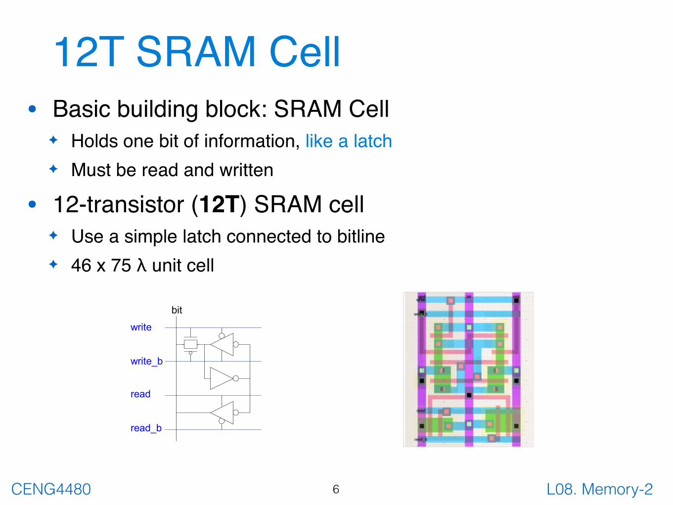
12T SRAM Cell• Basic building block: SRAM Cell
✦ Holds one bit of information, like a latch✦ Must be read and written
• 12-transistor (12T) SRAM cell✦ Use a simple latch connected to bitline✦ 46 x 75 λ unit cell
6
bit
write
write_b
read
read_b
L08. Memory-2CENG4480
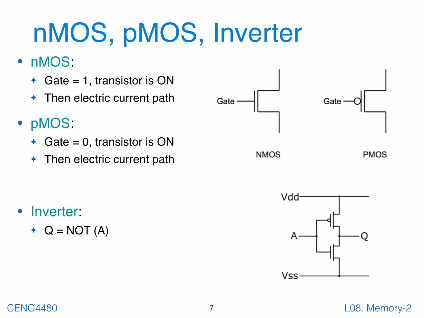
nMOS, pMOS, Inverter
7
• nMOS:✦ Gate = 1, transistor is ON✦ Then electric current path
• pMOS:✦ Gate = 0, transistor is ON✦ Then electric current path
• Inverter:✦ Q = NOT (A)

L08. Memory-2CENG4480
6T SRAM Cell• Used in most commercial chips
• A pair of weak cross-coupled inverters
• Data stored in cross-coupled inverters
• Compared with 12T SRAM, 6T SRAM:✦ (+) reduce area✦ (-) much more complex control
8
bit bit_b
word
L08. Memory-2CENG4480
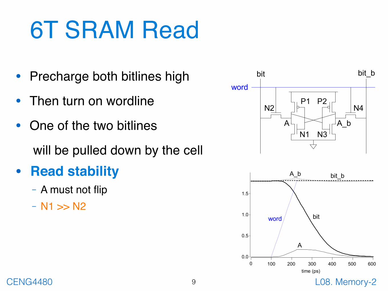
6T SRAM Read
• Precharge both bitlines high
• Then turn on wordline
• One of the two bitlines
will be pulled down by the cell
• Read stability– A must not flip– N1 >> N2
9
bit bit_b
N1
N2P1
A
P2
N3
N4
A_b
word
0.0
0.5
1.0
1.5
0 100 200 300 400 500 600time (ps)
word bit
A
A_b bit_b
L08. Memory-2CENG4480
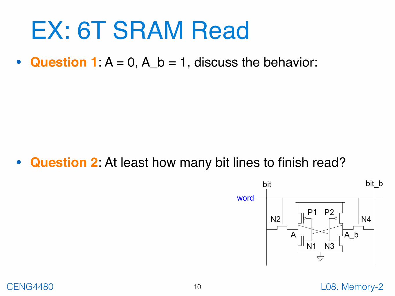
EX: 6T SRAM Read• Question 1: A = 0, A_b = 1, discuss the behavior:
• Question 2: At least how many bit lines to finish read?
10
bit bit_b
N1
N2P1
A
P2
N3
N4
A_b
word
L08. Memory-2CENG4480
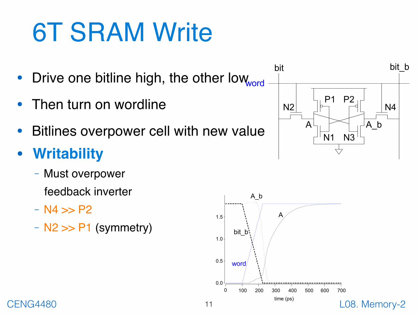
6T SRAM Write• Drive one bitline high, the other low
• Then turn on wordline
• Bitlines overpower cell with new value
• Writability– Must overpower feedback inverter– N4 >> P2– N2 >> P1 (symmetry)
11time (ps)
word
A
A_b
bit_b
0.0
0.5
1.0
1.5
0 100 200 300 400 500 600 700
bit bit_b
N1
N2P1
A
P2
N3
N4
A_b
word
L08. Memory-2CENG4480
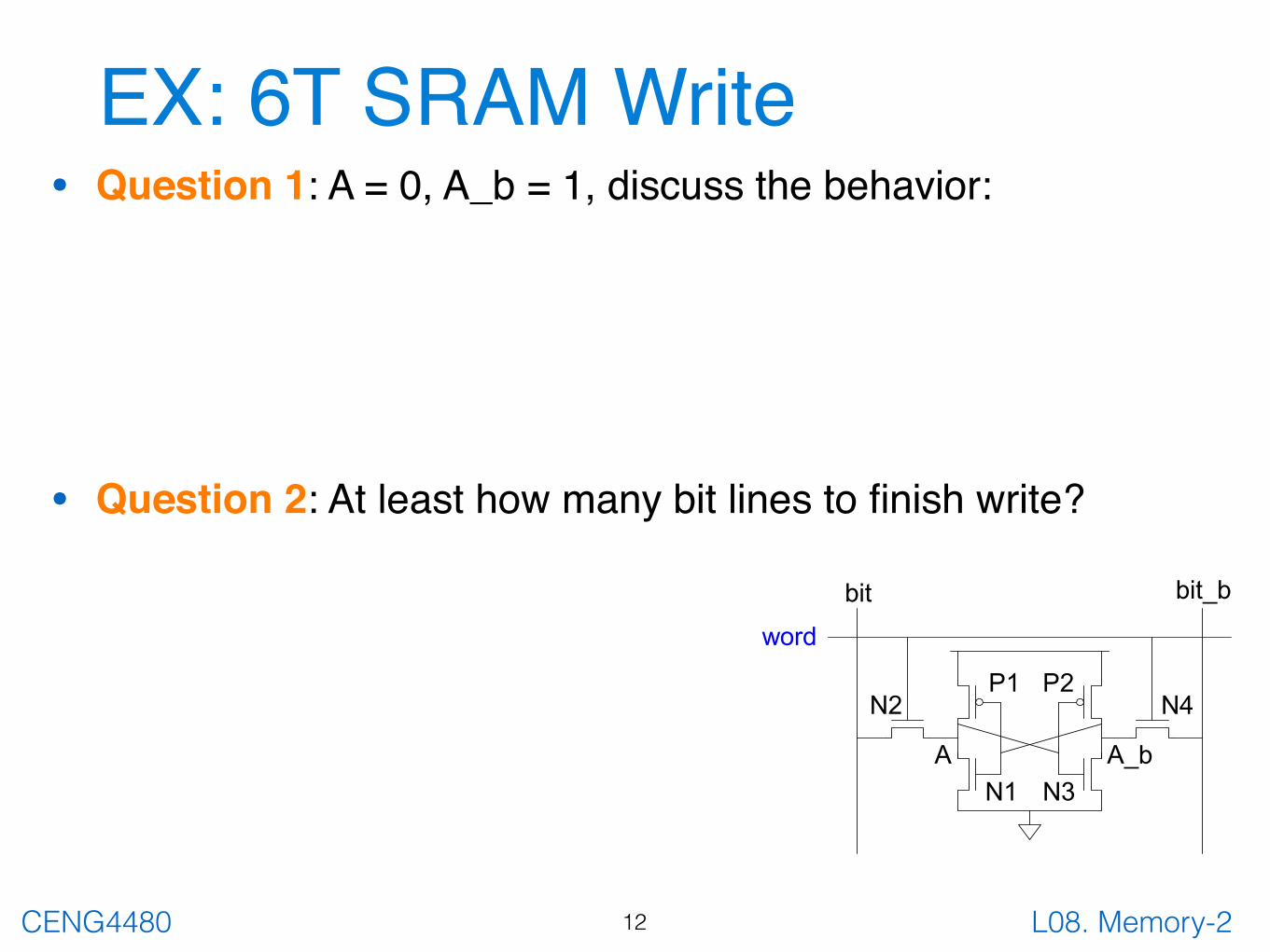
EX: 6T SRAM Write• Question 1: A = 0, A_b = 1, discuss the behavior:
• Question 2: At least how many bit lines to finish write?
12
bit bit_b
N1
N2P1
A
P2
N3
N4
A_b
word
L08. Memory-2CENG4480
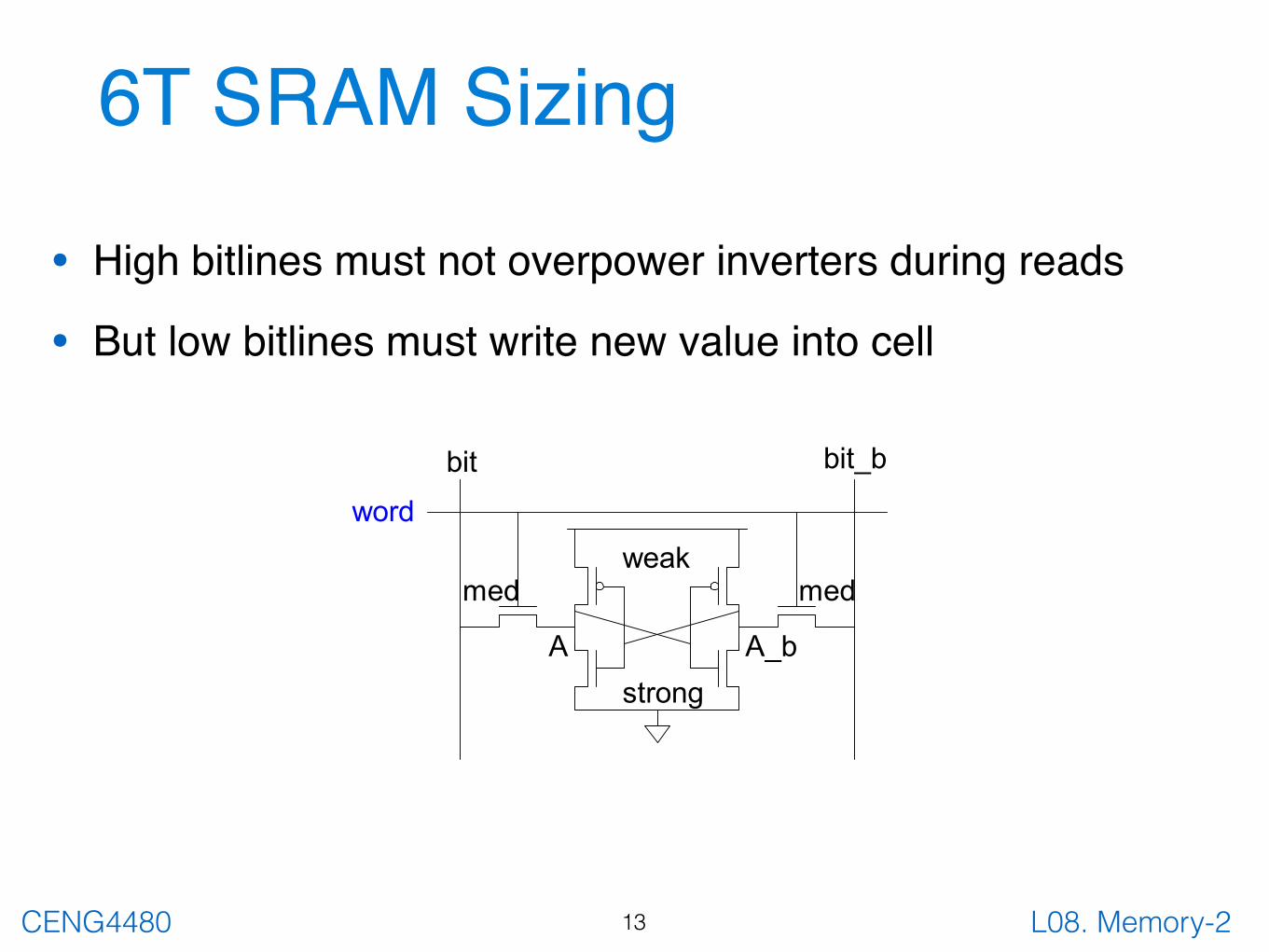
6T SRAM Sizing
• High bitlines must not overpower inverters during reads
• But low bitlines must write new value into cell
13
bit bit_b
med
A
weak
strong
med
A_b
word

L08. Memory-2CENG4480
Memory Arrays
Random Access Memory Serial Access Memory Content Addressable Memory(CAM)
Read/Write Memory(RAM)
(Volatile)
Read Only Memory(ROM)
(Nonvolatile)
Static RAM(SRAM)
Dynamic RAM(DRAM)
Shift Registers Queues
First InFirst Out(FIFO)
Last InFirst Out(LIFO)
Serial InParallel Out
(SIPO)
Parallel InSerial Out
(PISO)
Mask ROM ProgrammableROM
(PROM)
ErasableProgrammable
ROM(EPROM)
ElectricallyErasable
ProgrammableROM
(EEPROM)
Flash ROM
Memory Arrays
14
L08. Memory-2CENG4480
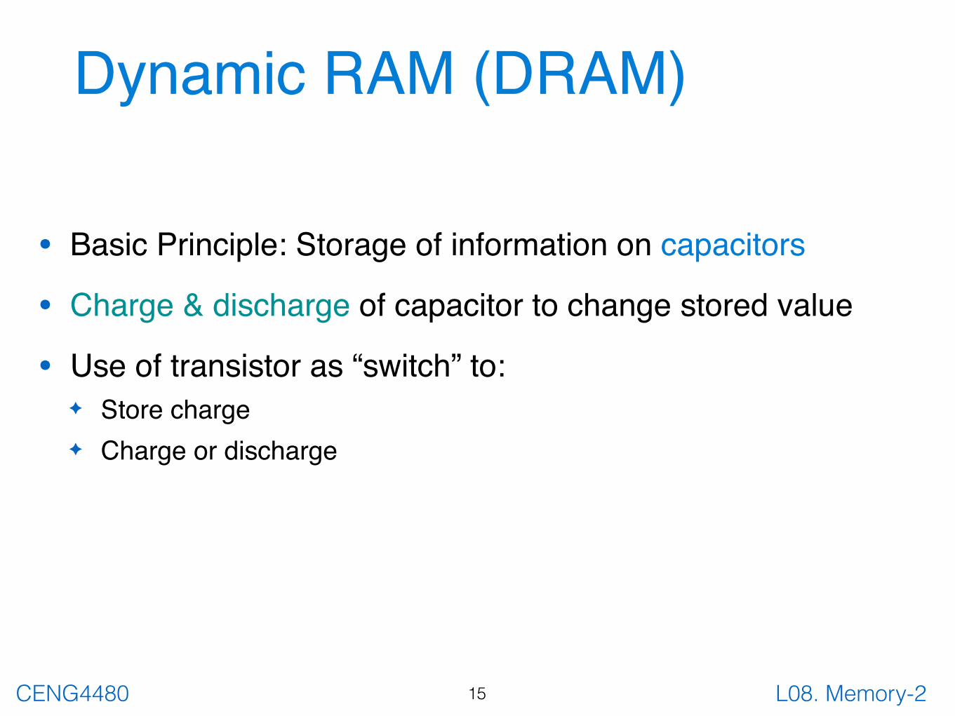
Dynamic RAM (DRAM)
• Basic Principle: Storage of information on capacitors
• Charge & discharge of capacitor to change stored value
• Use of transistor as “switch” to:✦ Store charge✦ Charge or discharge
15
L08. Memory-2CENG4480
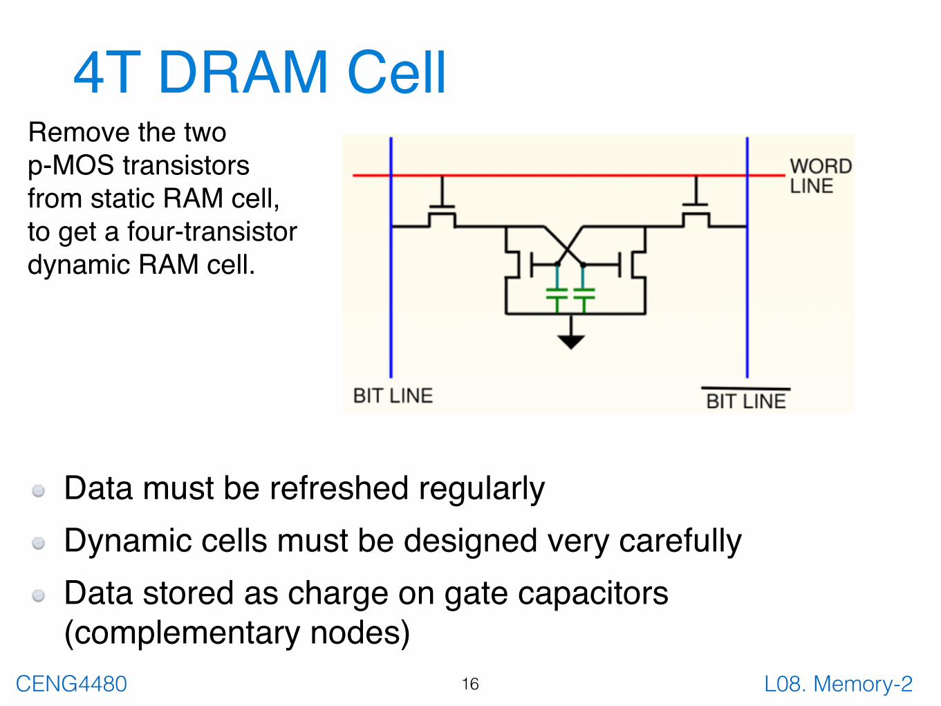
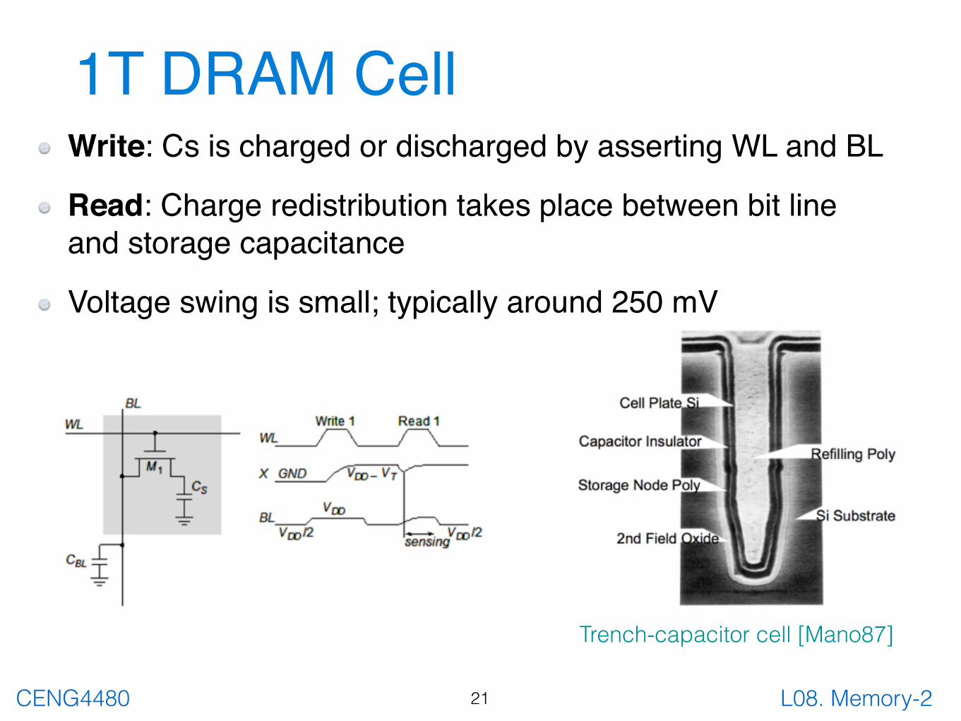
4T DRAM Cell
16
Data must be refreshed regularlyDynamic cells must be designed very carefullyData stored as charge on gate capacitors (complementary nodes)
Remove the twop-MOS transistors from static RAM cell,to get a four-transistordynamic RAM cell.
L08. Memory-2CENG4480
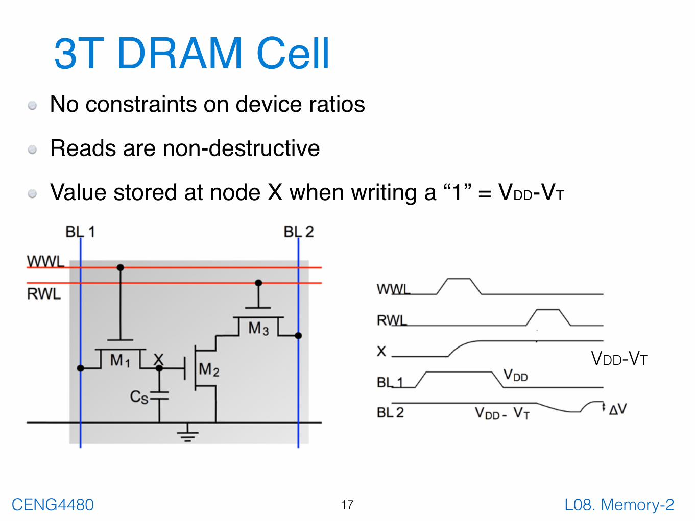
3T DRAM CellNo constraints on device ratios
Reads are non-destructive
Value stored at node X when writing a “1” = VDD-VT
17
VDD-VT
L08. Memory-2CENG4480
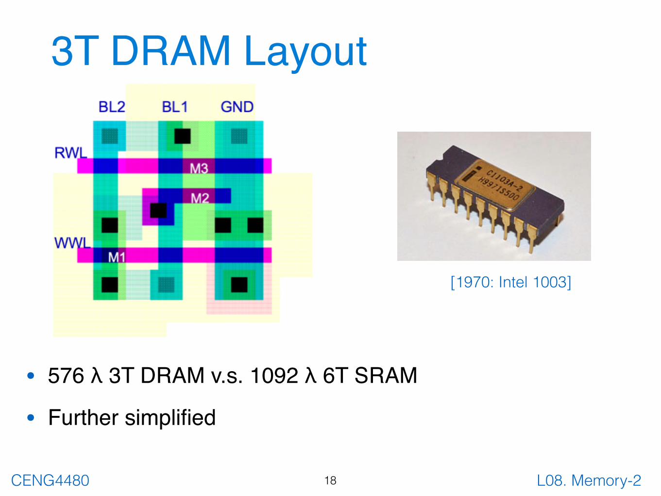
3T DRAM Layout
• 576 λ 3T DRAM v.s. 1092 λ 6T SRAM
• Further simplified
18
[1970: Intel 1003]

L08. Memory-2CENG4480
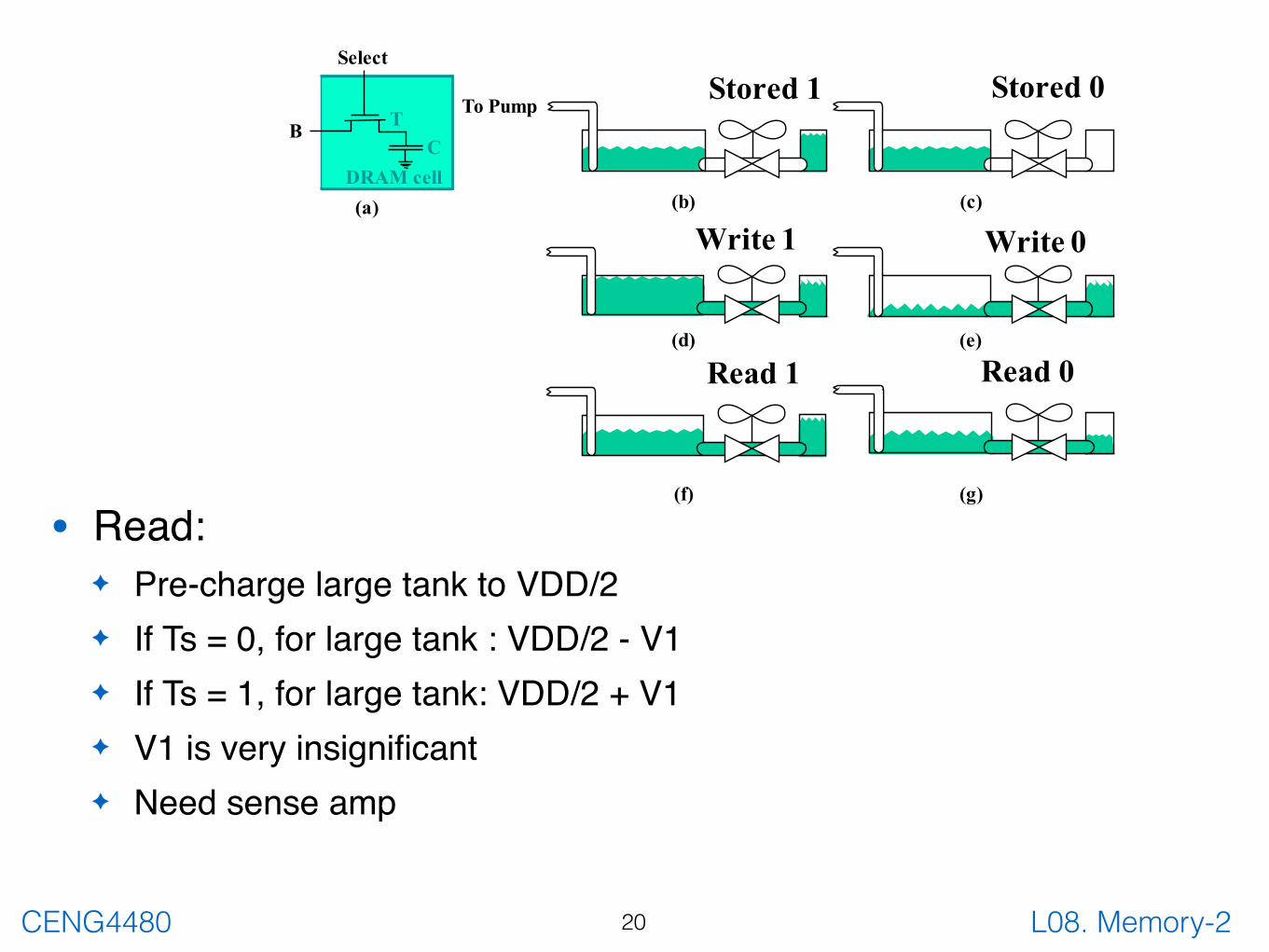
1T DRAM Cell
19
(a) (c)
(f) (g)
Select
B TC
DRAM cell
To Pump
(b)
(d) (e)
Stored 1 Stored 0
Write 1 Write 0
Read 1 Read 0
• Need sense amp helping reading
L08. Memory-2CENG4480
• Read:✦ Pre-charge large tank to VDD/2✦ If Ts = 0, for large tank : VDD/2 - V1✦ If Ts = 1, for large tank: VDD/2 + V1✦ V1 is very insignificant✦ Need sense amp
20
(a) (c)
(f) (g)
Select
B TC
DRAM cell
To Pump
(b)
(d) (e)
Stored 1 Stored 0
Write 1 Write 0
Read 1 Read 0
L08. Memory-2CENG4480
1T DRAM CellWrite: Cs is charged or discharged by asserting WL and BL
Read: Charge redistribution takes place between bit line and storage capacitance
Voltage swing is small; typically around 250 mV
21
Trench-capacitor cell [Mano87]

L08. Memory-2CENG4480
EX. 1T DRAM Cell• Question: VDD=4V, CS=100pF, CBL=1000pF. What’s
the voltage swing value?
• Note:
22
�V = VDD2 · CS
CS+CBL
L08. Memory-2CENG4480
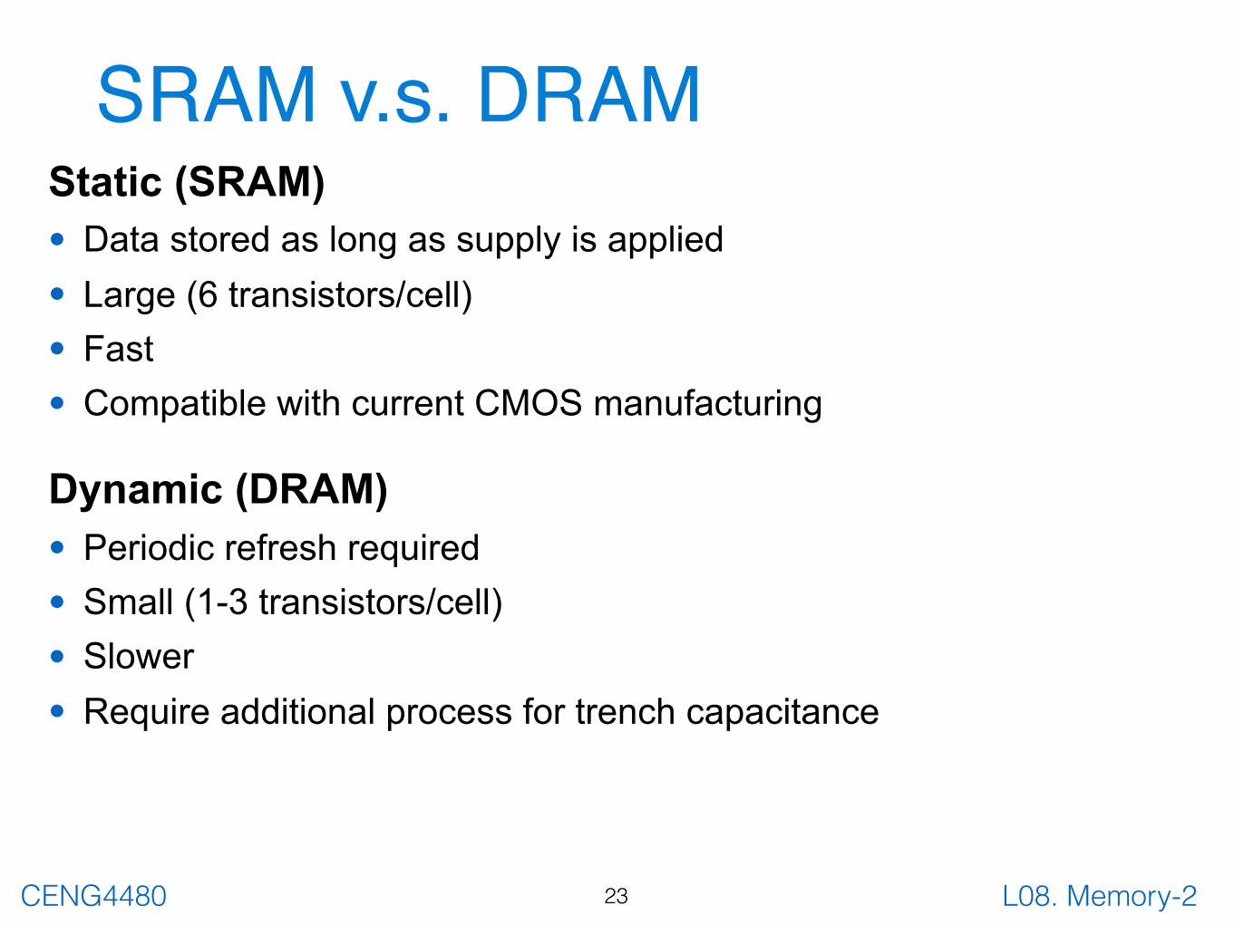
SRAM v.s. DRAMStatic (SRAM) • Data stored as long as supply is applied • Large (6 transistors/cell) • Fast • Compatible with current CMOS manufacturing
Dynamic (DRAM) • Periodic refresh required• Small (1-3 transistors/cell) • Slower • Require additional process for trench capacitance
23
L08. Memory-2CENG4480
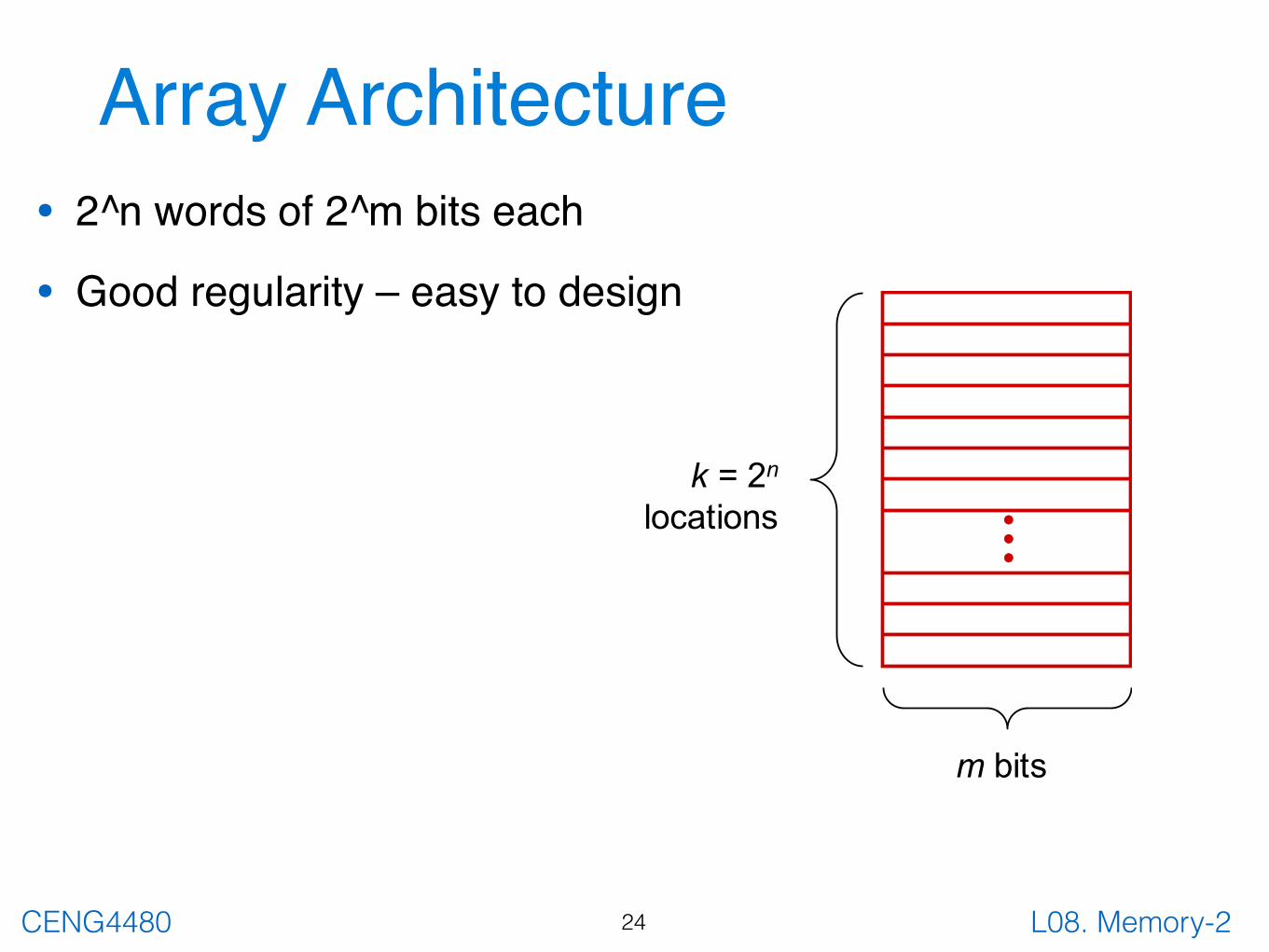
Array Architecture• 2^n words of 2^m bits each
• Good regularity – easy to design
24
•••
k ="2nlocations
m bits
L08. Memory-2CENG4480
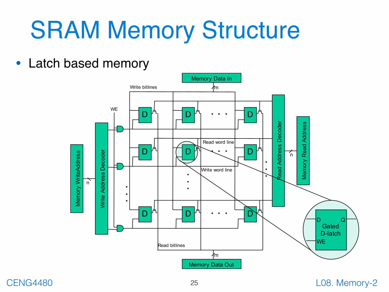
SRAM Memory Structure
25
n
D D D.$.$.
D D D.$.$.
D D D.$.$.
.$.$.
m
Memory$Data$Out
mMemory$Data$In
Read$Address$Decoder
Memory$Read$Address
n
Write$Address$Decoder
Memory$WriteAddress
GatedD8latch
D Q
WERead$bitlines
Write$bitlines
Write$word$line
Read$word$line
.$.$.
.$.$.
WE
• Latch based memory

L08. Memory-2CENG4480
Array Architecture• 2^n words of 2^m bits each
• How to design if n >> m?
• Fold by 2k into fewer rows of more columns
26
row decoder
columndecoder
n
n-kk
2m bits
columncircuitry
bitline conditioning
memory cells:2n-k rows x2m+k columns
bitlines
wordlines
L08. Memory-2CENG4480
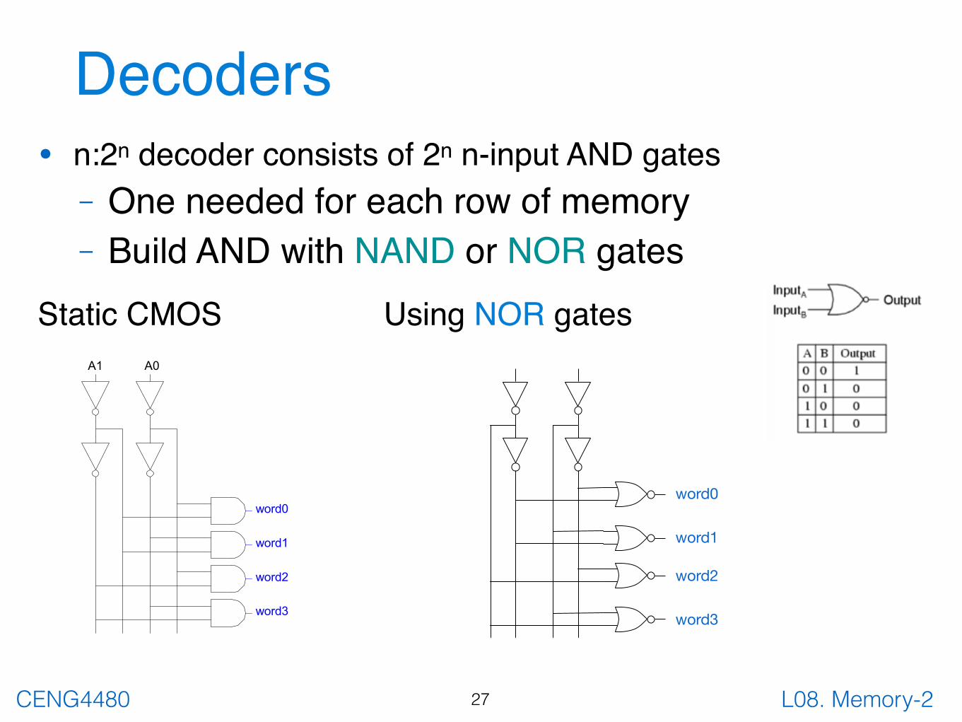
Decoders• n:2n decoder consists of 2n n-input AND gates
– One needed for each row of memory– Build AND with NAND or NOR gates
Static CMOS Using NOR gates
27
word0
word1
word2
word3
A0A1
word0
word1
word2
word3
L08. Memory-2CENG4480
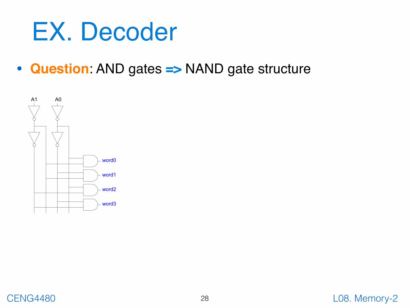
EX. Decoder• Question: AND gates => NAND gate structure
28
word0
word1
word2
word3
A0A1

L08. Memory-2CENG4480
Large Decoders• For n > 4, NAND gates become slow
– Break large gates into multiple smaller gates
29
word0
word1
word2
word3
word15
A0A1A2A3
L08. Memory-2CENG4480
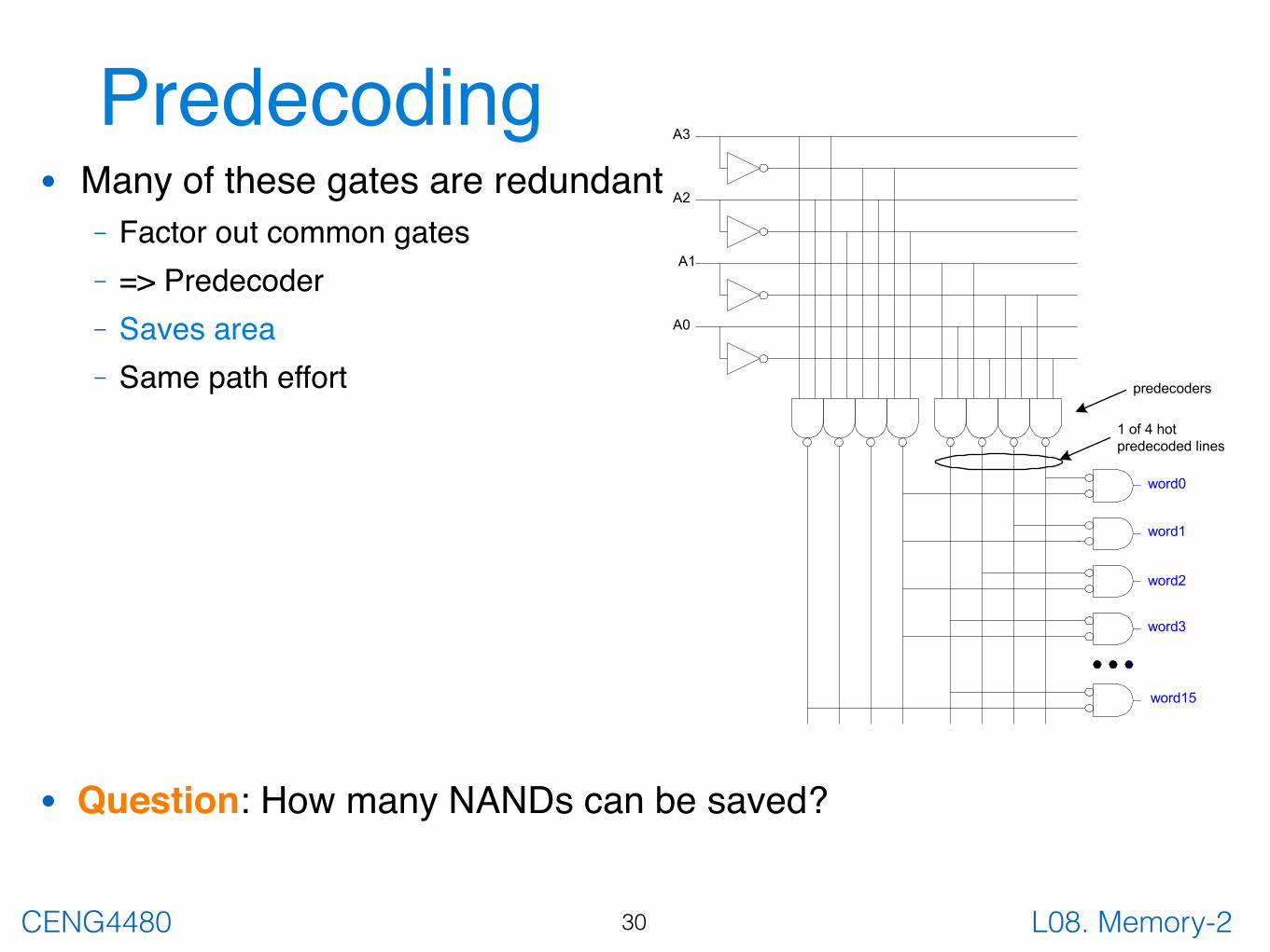
Predecoding• Many of these gates are redundant
– Factor out common gates– => Predecoder– Saves area– Same path effort
• Question: How many NANDs can be saved?
30
A0
A1
A2
A3
word1
word2
word3
word15
word0
1 of 4 hotpredecoded lines
predecoders

L08. Memory-2CENG4480
Decoder Layout• Decoders must be pitch-matched to SRAM cell
– Requires very skinny gates
31
GND
VDD
word
buffer inverterNAND gate
A0A0A1A2A3 A2A3 A1
L08. Memory-2CENG4480
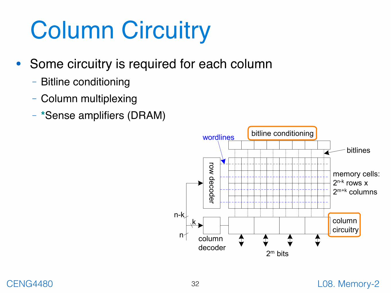
Column Circuitry• Some circuitry is required for each column
– Bitline conditioning– Column multiplexing– *Sense amplifiers (DRAM)
32
row decoder
columndecoder
n
n-kk
2m bits
columncircuitry
bitline conditioning
memory cells:2n-k rows x2m+k columns
bitlines
wordlines
L08. Memory-2CENG4480
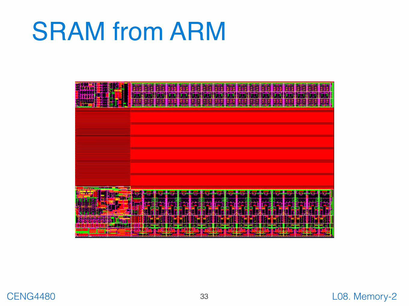
SRAM from ARM
33

L08. Memory-2CENG4480
Bitline Conditioning• Precharge bitlines high before reads
• Equalize bitlines to minimize voltage difference when using sense amplifiers
34
φbit bit_b
φ
bit bit_b
L08. Memory-2CENG4480
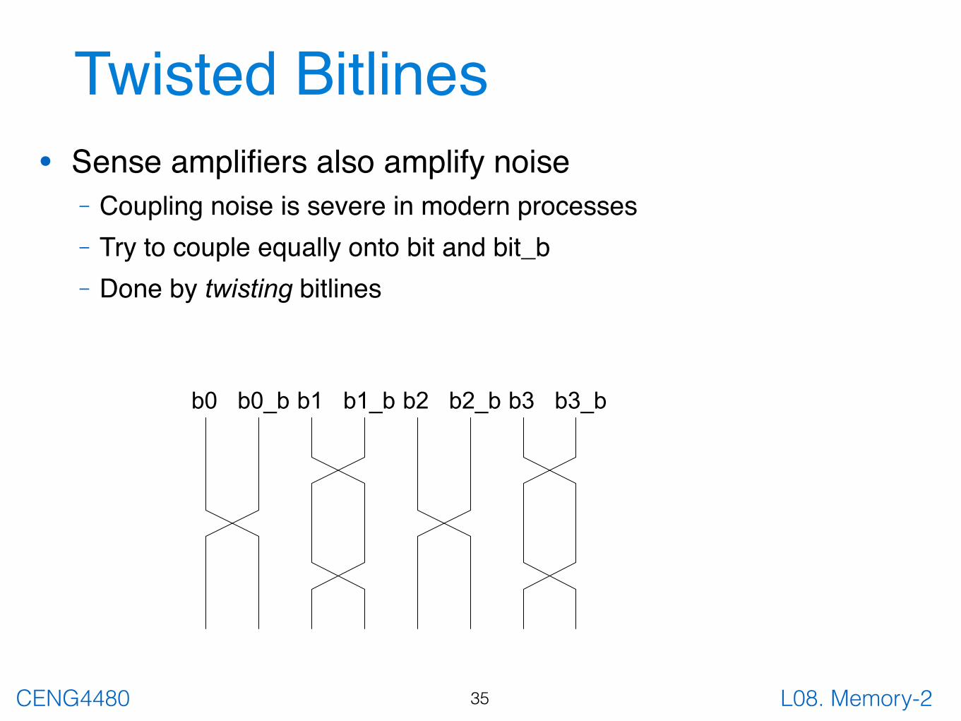
Twisted Bitlines• Sense amplifiers also amplify noise
– Coupling noise is severe in modern processes– Try to couple equally onto bit and bit_b– Done by twisting bitlines
35
b0 b0_b b1 b1_b b2 b2_b b3 b3_b
L08. Memory-2CENG4480
SRAM Column Example
Read Write
36
H H
SRAM Cell
word_q1
bit_v1f
bit_b_v1f
out_v1rout_b_v1r
φ1
φ2
word_q1
bit_v1f
out_v1r
φ2
MoreCells
Bitline Conditioning
φ2
MoreCells
SRAM Cell
word_q1
bit_v1f
bit_b_v1f
data_s1
write_q1
Bitline Conditioning

L08. Memory-2CENG4480
Column Multiplexing
• Recall that array may be folded for good aspect ratio
• Ex: 2 kword x 16 folded into 256 rows x 128 columns– Must select 16 output bits from the 128
columns– Requires 16 8:1 column multiplexers
37

L08. Memory-2CENG4480
Ex: 2-way Muxed SRAM
38
MoreCells
word_q1
write0_q1
φ2
MoreCells
A0
A0
φ2
data_v1
write1_q1
14. Memories
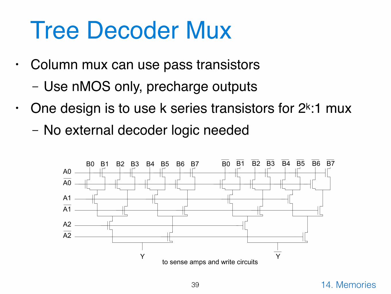
Tree Decoder Mux• Column mux can use pass transistors
– Use nMOS only, precharge outputs• One design is to use k series transistors for 2k:1 mux
– No external decoder logic needed
39
B0 B1 B2 B3 B4 B5 B6 B7 B0 B1 B2 B3 B4 B5 B6 B7A0
A0
A1
A1
A2
A2
Y Yto sense amps and write circuits
L08. Memory-2CENG4480
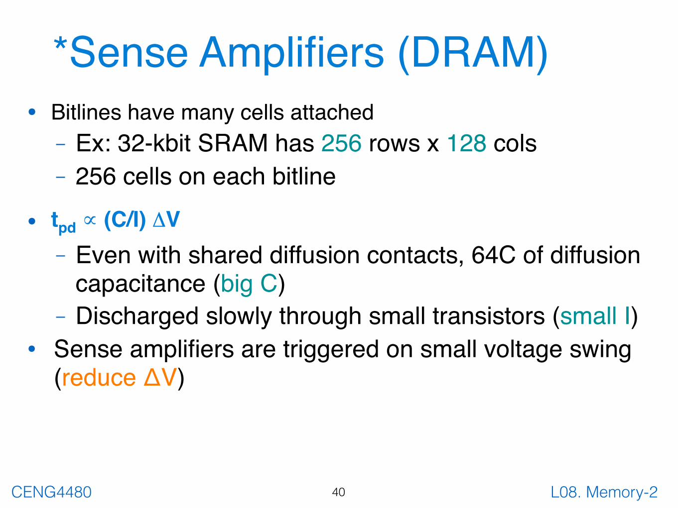
*Sense Amplifiers (DRAM)• Bitlines have many cells attached
– Ex: 32-kbit SRAM has 256 rows x 128 cols– 256 cells on each bitline
• tpd ∝ (C/I) ΔV– Even with shared diffusion contacts, 64C of diffusion
capacitance (big C)– Discharged slowly through small transistors (small I)
• Sense amplifiers are triggered on small voltage swing (reduce ΔV)
40
L08. Memory-2CENG4480
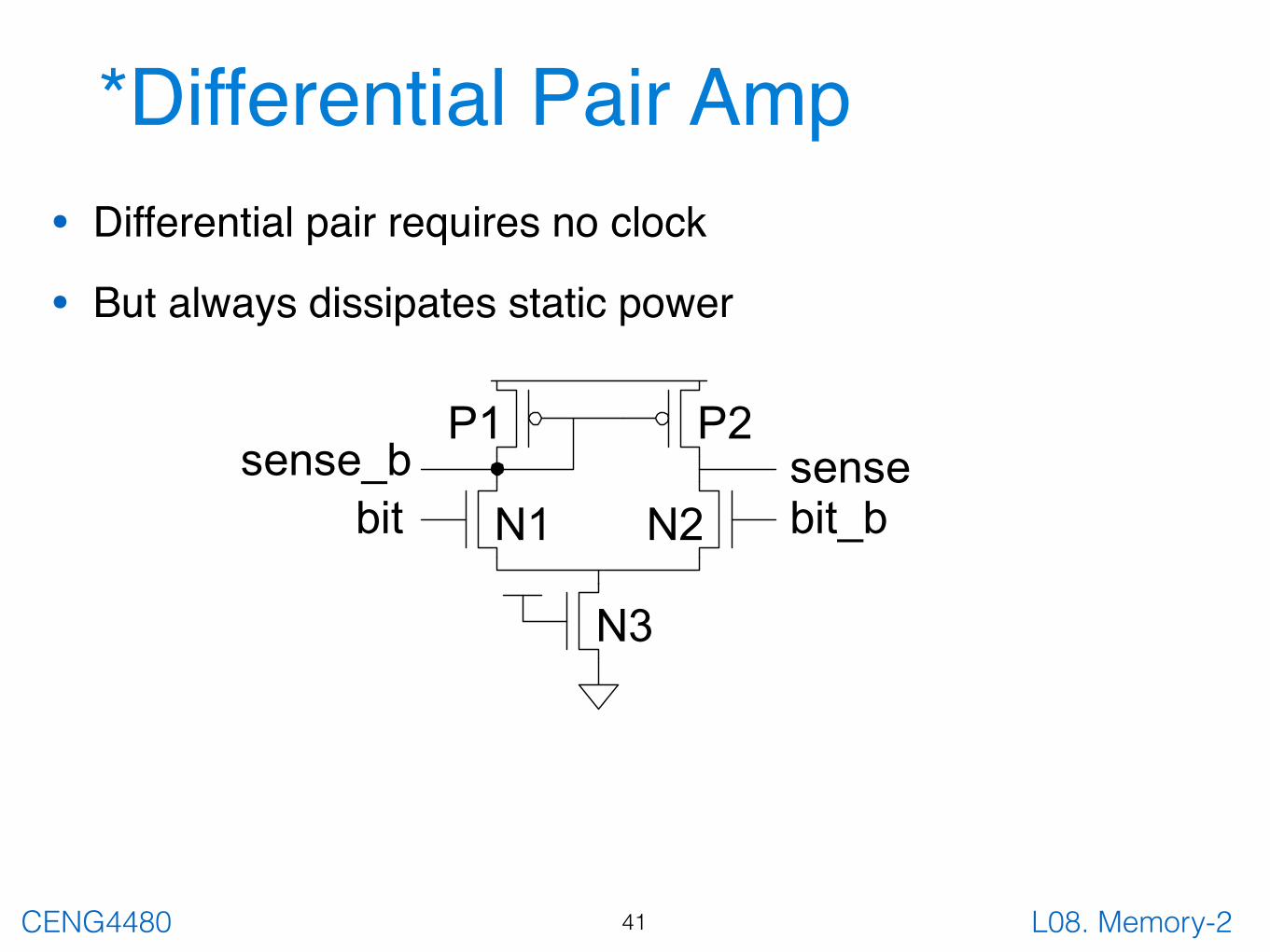
*Differential Pair Amp• Differential pair requires no clock
• But always dissipates static power
41
bit bit_bsense_b sense
N1 N2
N3
P1 P2

L08. Memory-2CENG4480
*Clocked Sense Amp• Clocked sense amp saves power
• Requires sense_clk after enough bitline swing
• Isolation transistors cut off large bitline capacitance
42
bit_bbit
sense sense_b
sense_clk isolationtransistors
regenerativefeedback
L08. Memory-2CENG4480
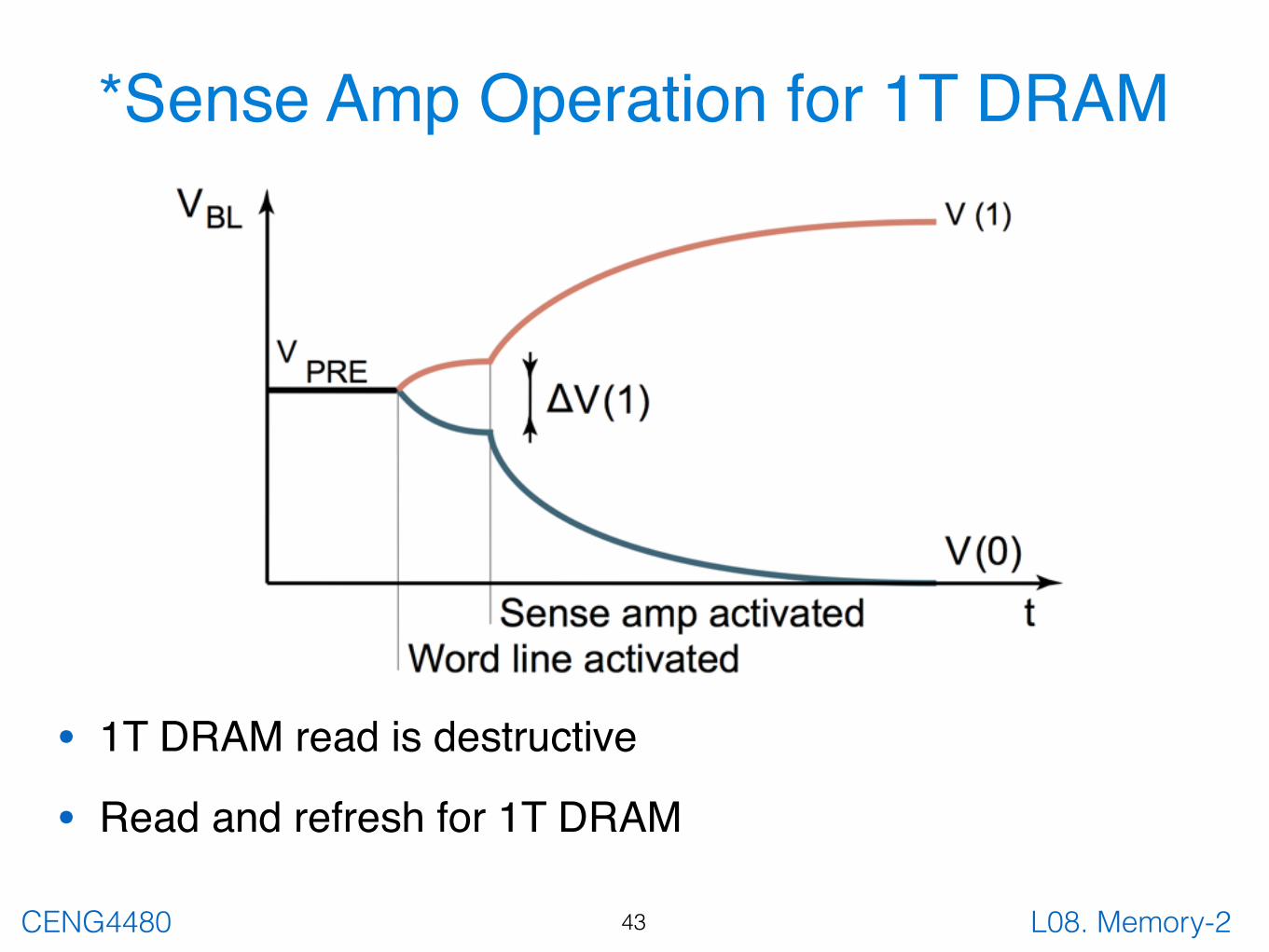
*Sense Amp Operation for 1T DRAM
• 1T DRAM read is destructive
• Read and refresh for 1T DRAM
43

L08. Memory-2CENG4480
Thank You :-)
44