ch 9.1-.5, .9, app b-3: ch 9, lab 6: ch9 pr 1,3*, 4*, 5,...
TRANSCRIPT
Physics 310
Lecture 6b – Op Amps
1
Fri. 2/19 Ch 9.1-.5, .9, App B-3: Operational Amplifiers HW5: * ; Lab 5 Notebook
Mon. 2/22
Wed. 2/24
Thurs. 2/25
Fri. 2/26
Ch 9, the rest
Quiz Ch 9, Lab 6: Operational Amplifiers
More of the same
Midterm Review (through Transistors)
HW 6: Ch9 Pr 1,3*, 4*, 5, 21
Lab 6 Notebook
Announcements
Midterm just after break.
Handout (in lecture):
Lab #6
9-6 Mathematical Functions: Addition, Differentiation, Integration
One of the swell things about op-amps is that you can build circuits with them that perform
mathematical operations. On the one hand, that‟s a cute novelty item – a circuit that will add,
integrate, or differentiate for you. No matter how non-analytical the input function may be, the
circuit happily integrates or differentiates it for you! On the other hand, these are very common
signal-processing operations; within the context of a large circuit, you‟ll often find little „adder‟,
„integrator‟, and „differentiator‟ blocks.
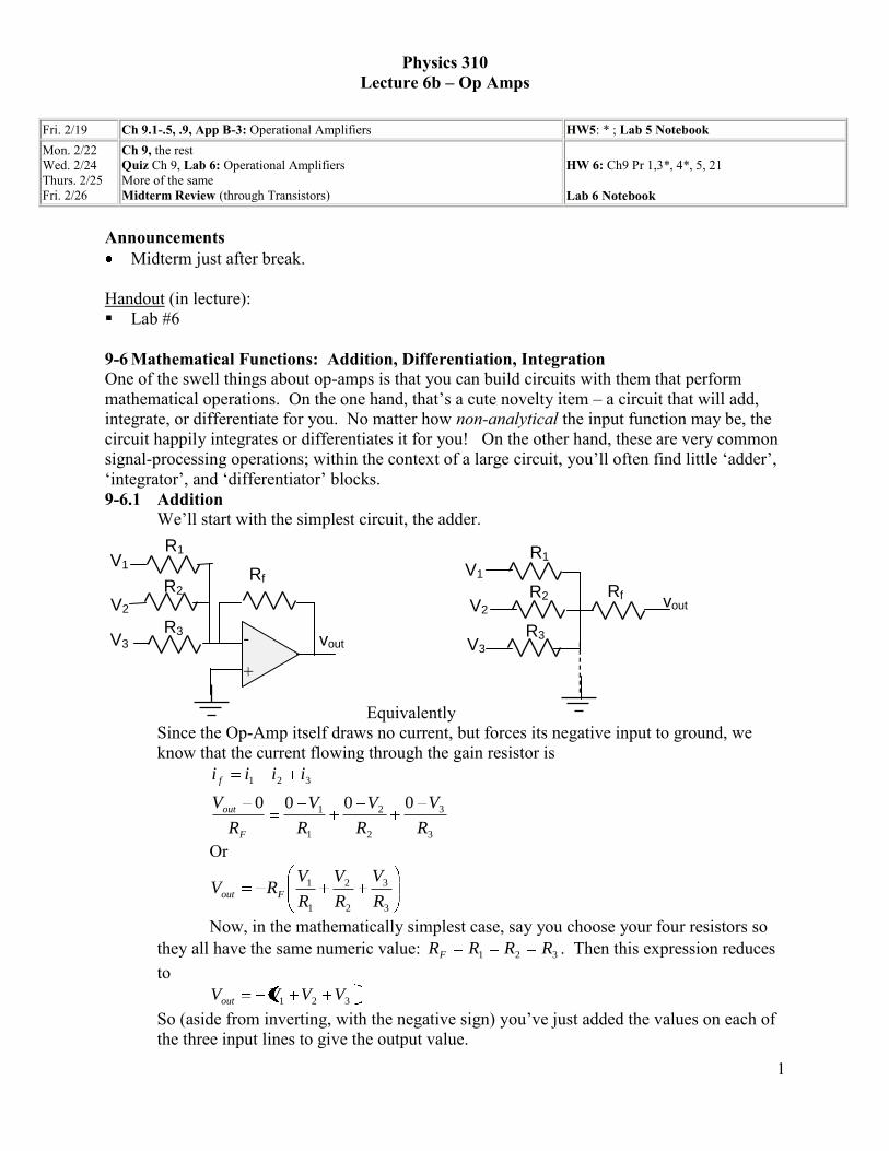
9-6.1 Addition
We‟ll start with the simplest circuit, the adder.
vout
R1
-
+
Rf V1
V2
R2
R3 V3
Equivalently
R2
R3
V1
vout
R1
Rf V2
V3
Since the Op-Amp itself draws no current, but forces its negative input to ground, we
know that the current flowing through the gain resistor is
3
3
2
2
1
1
321
0000
R
V
R
V
R
V
R
V
iiii
F
out
f
Or
3
3
2
2
1
1
R
V
R
V
R
VRV Fout
Now, in the mathematically simplest case, say you choose your four resistors so
they all have the same numeric value: 321 RRRRF . Then this expression reduces
to
321 VVVVout
So (aside from inverting, with the negative sign) you‟ve just added the values on each of
the three input lines to give the output value.

Physics 310
Lecture 6b – Op Amps
2
Of course, you could also weight each input signal differently. For example, say you
wanted Vout = -(1*V1 +10*V2+100*V3) that‟s easily achieved by choosing the right
resistors.
9-6.2 Integration (I do)
We go back to the simple inverting-amplifier configuration and replace the gain resistor
with a capacitor to have this.
vout
R1
-
+
C
Vin
Equivalently
vout
R1 C
Vin
Looking at the flow of charge,
dt
dq
R
v
iR
v
cin
R
0
(I‟m using lower case since we‟re likely considering time varying
voltages, currents, and charges.)
Where what I mean by qc is the charge on the left side of the capacitor.
Now, as for the capacitor,
0outc
cc
vCq
vCq
(as with the sign in Ohm‟s law, books usually ignore the sign here,
but it means that if you‟ve got a positive charge on the left, then
you‟ve got a voltage drop from left to right.)
So, substituting this in for the charge in the derivative,
dt
dvCvC
dt
d
dt
dqi
R
v out
out
cin )0(0
1
Flipping around to solve for Vout gives t
inCRout tdtvtv0
1 )()(1
The output is the (scaled and inverted) time-integral of the input!
Remember the simple RC circuit which only approximated an integrator for the right
range of frequencies. Now, this circuit is an integrator (to as many sig figs as 1/A = 0 and as
long as the frequency isn‟t insanely high).

Physics 310
Lecture 6b – Op Amps
3
9-6.3 Differentiation (They do)
If you flip the R and the C, you flip the job this performs, form integrating to
differentiating.
vout
R
-
+
C
Vin
Equivalently
vout
R C Vin
Again, being specific about signs, the relationship between a capacitor‟s charge and
voltage drop is
cc vCq
In this case,
inc vv 0
so,
cin qCv
While the relationship between a resistor‟s current and voltage drop is
R
vi R
Where the current flowing through the resistor (implicitly to the right) equals the rate of
charge flowing onto the capacitor (from the left):
dt
dqi c
dt
dvRCv
dt
dCv
dt
dqi
R
v
in
out
inLeftout
Tada! The output voltage is equal to the (negative) derivative of the input voltage, times
RC.
9-8 Filters
We‟ve seen how an Op-Amp can be used as an Integrator and how one can be used as a
Differentiator. Now, you‟ve previously seen similar combinations or R‟s and C‟s (without the
Op-Amps) in “RC” filters. You can see that the Integrator and Differentiator can perform a
similar function – Preferentially „passing‟ either high or low frequency signals.
Differentiator – High-Pass Filter / Amplifier
The differentiator‟s output and input are related by
dt
dvRCv in
out

Physics 310
Lecture 6b – Op Amps
4
So, if the input voltage varies sinusoidally, )sin()( tVtv inin, then the output would be
.cos)()( tVRCtvdt
dRCtv ininout
Notice that the bigger is, i.e., the higher the frequency is, the bigger the output signal
is. More specifically,
inoutRC
inoutRC
VV
VV
1
1
This is essentially a High Pass filter and an amplifier combined.
Integrator – Low-Pass Filter / Amplifier
On the other hand, the Integrator‟s output and input are related by
t
inCRout tdtvtv0
1 )()(1
Again, if the input voltage varies sinusoidally, )sin()( tVtv inin, then the output would
be
tVtdtvtv inCR
t
inCRout cos1
)()(11
1
0
1
In this case, the smaller , i.e., the lower the frequency is, the bigger the output signal is.
More specifically,
inoutRC
inoutRC
VV
VV
1
1
This is essentially a Low Pass filter and amplifier.
9-8.1 Integrator-Differentiator
Now, let‟s say we put the two together! A Low-Pass Filter Integrator and a High-Pass Filter
Differentiator: we get a Band – Pass Integrator-Differentiator. We might qualitatively guess
that most frequencies come through weakly, but right around the sweet spot of RC
1the
signal comes through loud and clear. Let‟s see how this plays out.
vout
Rf
-
+
C1
Vin
R1
Cf
or
vout R1 C1
Vin
Rf
Cf
This circuit has a complex enough mixture of impeding elements, resistors and capacitors, that
we‟re going to want to use Phasors to analyze it.

Physics 310
Lecture 6b – Op Amps
5
Following the current flow across the circuit,
f
outin
f
Z
V
Z
V
II
00
1
1
So,
1Z
ZVV
f
inout
Where, the two elements in series add up to 1
11111 CC jRZRZ
While the two elements in parallel add up to fRZR
fjC
Z
fCff
111
11
So,
11
1
1
11
111
111
CRfC
C
R
Rin
fRC
inout
f
f
ffCRj
VjCjR
VV
In Amplitude-Phase notation, that‟s
1
1
1
11
1
11
1
tan
211
2
1 C
fC
fR
R
CfRf
f
f
f
CR
j
CRfC
C
R
Rinout e
CR
VV
Obviously, the denominator minimizes (the output voltage maximizes) and the phase shift is just
the -1 that‟s out front, at the frequency o for which
01
11 of CRofCR or
ff
oCRCR 11
1
There we have the predicted sweet-spot frequency.
A plot of Vout vs. frequency would look something like
A common measure of a peak‟s width is the “full-width at half-max.” As the
name suggests, it‟s how far apart (in frequency, in this case) are the two points at which
the curve drops to half its maximal value. So, it can be found by returning to the
expression for Vout and setting its amplitude equal to half the peak, then solving for the
frequencies that satisfy that condition – the difference between these two frequencies is
the width of the peak. Skipping all that work, this peak‟s width is
22
1
2 6 of where ff
fCR
1and
11
1
1
CR;
1
1max.
C
C
R
R
in
outf
f
VV
outV
o
max.21
outV

Physics 310
Lecture 6b – Op Amps
6
in those terms, 1
2
fo
One thing we can read from this is that, in absolute terms, the higher the circuit‟s
designed pass-frequency, o, the wider the peak, but in relative terms (relative to the
pass-frequency), the peak isn‟t exactly dependent on the frequency, rather it depends on
how well balanced f and 1 are, with a minimum if f = :
861
1 f
f
o
9-8.2 Twin-T Filter
Strictly speaking, this would have fit better in Ch. 2; however, it‟s good review (test
coming up) and we‟ll use it with an op-amp in a moment. First we‟ll consider a Twin-T
filter all by itself (that we could have done back in chapter 2) and then we‟ll see how it
can be incorporated in an Op-Amp circuit.
All by itself, the Twin-T filter has an impedance that peaks at a specific frequency – that
means it‟s a notch-pass filter. That is, the output spectrum looks like a notch was cut out
of it – most frequency signals pass without a problem, but not right around o.
vout
R
C Vin
C
R
2C R/2
vout R
C
Vin
C
R
2C
R/2
Qualitatively, there are a high pass filter (blue) and a low pass filter (red) in parallel. So
a signal with a high frequency is blocked on the red branch, but, no matter, it passes
along the blue branch. Similarly, a low-frequency signal is blocked on the blue branch
but passes along the red branch. In contrast, a signal with frequency around RC
o
1
has trouble down either branch.
Quantitatively, it‟s easier to analyze the circuit if we look at it like this (all the same
connections, just twisted around a bit.)
Or,
unwrapping
it a bit

Physics 310
Lecture 6b – Op Amps
7
R
C
C
R 2C
R/2
Vin
vout
a
b
c
d
Not counting vin and vout, we have 4 equations and 4 unknowns (the currents), so a
relationship can be constructed for vout in terms of vin, R, and ZC. Without going through
all the motions, that relationship is
o
o
j
vv in
out
41
(based on eq‟n 3-82 and Fig. 3-17 of J.J. Brophy‟s Basic
Electronics for Scientists, where the C‟s and R‟s assume
the values to match Fig 9.17 of Diefenderfer‟s book.)
or, in amplitude – phase notation,
o
o
o
o
j
in
out ev
v
4tan
2
1
41
where RC
o
1.
Strikingly, vout doesn‟t just get small at o; it vanishes! For that matter, when we‟re far
from o, vout approaches vin.
inout VV max.
outV
o
inV21
One way to tackle this is
to consider four loops:
Applying the Loop Rule to each gives
a) 2/)( Riiziiv cacbain where C
jZC
1
b) CabCcbdbb ZiiZiiRiiRi0
c) 2/Riiziiv accbcout
d) Cdbdout ziRiiv 2

Physics 310
Lecture 6b – Op Amps
8
A similar full-width at half-max analysis to that used for the Integrator-Differentiator
Filter reveals a width of o3
4, or a relative width of
3
4
o
which is slightly
narrower than the best that the Integrator-Differentiator could do (when f1 ),
2
48 .
Impedance. In terms of impedance, the impedance of Twin-T filter vanishes far from o
and explodes at o
0TZ for o or o
TZ as o
Frequency Switch. This is kind of like a switch: for most frequency signals, the
switch is closed – allowing the signal to pas; for signals with frequency o, the
switch is flung open – blocking the signal.
With an Op-Amp. This Twin-T filter could be used on its own, or it could be used in
conjunction with an Op-Amp (that‟s the chapter we‟re in, after all). Again, the reason for
going this rout rather than using a simple Integrator-Differentiator configuration is that
the Twin-T is more selective (narrower band).
For thinking how it might work with an op-amp, it‟s handy to think in terms of the
impedance. Let‟s look back at the simple inverting amplifier configuration.
vout
R1
-
+
Rf
Vin
Now, say we augment R1 with a Twin-T,
vout
R1 -
+
Rf
Vin Twin-T
ZT
So, the output voltage should be
T
f
inoutZR
RVV
1
Now, for frequencies far from o, the Twin-T is as good as not-there (no impedance),
and, just as usual,

Physics 310
Lecture 6b – Op Amps
9
vout
R1
-
+
Rf
Vin
1R
RVV
f
inout when o or o
But when in the vicinity of o the impedance blows up, killing the output
vout
R1
-
+
Rf
Vin
0f
inout
RVV
This isn‟t too surprising, we essentially have a Twin-T in series with an Inverting
Amplifier, so of courses the amplifier‟s signal cuts out when the Twin-T kills its input signal.
On the other hand, we could augment the gain resistor, Rf, with the Twin-T.
vout
R1 -
+
Rf
Vin
Twin-T
ZT
Now, 1
/
R
RZZRVV
fTTf
inout
Right around o , ZT goes infinite, so it‟s like having an open switch above the gain
resistor. In that case, the we simply have
vout
R1 -
+
Rf
Vin
1R
RVV
f
inout As if the Twin-T weren‟t there.
Physics 310
Lecture 6b – Op Amps
10
Far from this frequency, the Twin-T has no resistance, so we‟ve essentially got
vout
R1 -
+
Rf
Vin
Vout = 0
So the gain resistor is shorted out and we‟ve got a follower with an input of ground.
Sure, there‟s a Vin on the other side of R1, but if the Op-Amp‟s doing it‟s thing, it‟s
forcing V-=V+ and V+ = 0.
The advantage of using a complicated Twin-T filter rather than a simple Integrator-
Differentiator one is that, as already noted, the Twin-T filter is more selective:
9-7 Current Amplifiers
The point of many circuits is manipulating a “signal” that is represented by a voltage –
multiply the signal, integrate the signal, add the signal to another one… Sometimes
though, the salient property is a current, not a voltage. For example, your measure a
current, and you want to translate that “signal” into a voltage (for adding, integrating,…),
or perhaps your building a power supply so you want to be able to boost up a current. So,
here are a couple of op-amp circuits that focus in on the current rather than the voltage.
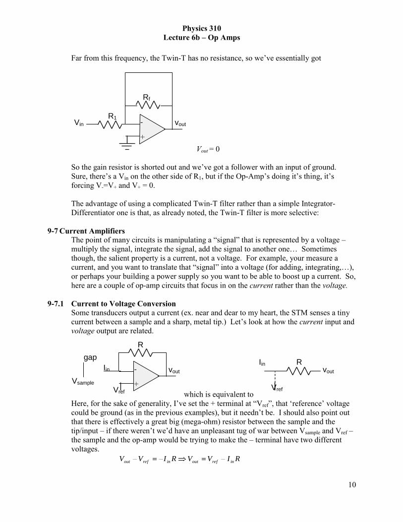
9-7.1 Current to Voltage Conversion
Some transducers output a current (ex. near and dear to my heart, the STM senses a tiny
current between a sample and a sharp, metal tip.) Let‟s look at how the current input and
voltage output are related.
vout
R
-
+
Iin
Vref
gap
Vsample
which is equivalent to
vout
R Iin
Vref
Here, for the sake of generality, I‟ve set the + terminal at “Vref”, that „reference‟ voltage
could be ground (as in the previous examples), but it needn‟t be. I should also point out
that there is effectively a great big (mega-ohm) resistor between the sample and the
tip/input – if there weren‟t we‟d have an unpleasant tug of war between Vsample and Vref –
the sample and the op-amp would be trying to make the – terminal have two different
voltages.
RIVVRIVV inrefoutinrefout

Physics 310
Lecture 6b – Op Amps
11
9-7.2 Current-to-Current Amplifier
Say you want to amplify a current.
Iout
Rf
-
+
Iin RL
Rs If= Iin Is
equivalently
vout
RL
Rf
Rs
Iin Is
Iout
While the actual circuit may not be crystal clear, the equivalent one is. Looking at that,
from the Node Rule:
sinout III ,
From the Loop Rule:
s
f
insssfin
sf
R
RIIRIRI
VV
Putting this together with the Iout expression gives
s
f
inout
s
f
ininout
R
RII
R
RIII
1
So, how much bigger the output current is than the input current depends on these two
resistances. Rather remarkably, the current through the load resistor, Iout, is independent of the
load resistance (for an ideal op-amp anyway), since the op-amp will adjust its Vout value to be
whatever it needs to be in order to maintain equal voltage it its two input terminals, V+=V-.
9-10 Real Op-Amps
For a while now, we‟ve been idealizing the Op-Amp: it draws no current( inZ ), it can
source as much current as you want ( 0outZ ), it has infinite gain, ( A ), and there‟s no
limit to how big Vout can be. In most applications, they‟re as good as true, but none are
absolutely true. Actually, when we talked about the Comparator, we admitted and made use
of the fact that Vout was bounded by the + and – power lines. Now we‟ll amend the other
idealizations and consider their impact on circuit design. For a given make & model of Op-
Amp, the manufacturer produces documentation that, among other things, characterizes these
imperfections – to help the user select the appropriate Op-Amp for his/her application.
9-10.1 Gain
Let‟s return to the simple Inverting Amplifier, and analyze it a little more rigorously to
see just how the output depends on the gain value, A – something that‟s often on the
order 104, but we usually like to idealize as infinite. How much does the difference
between infinity and 104 usually matter?

Physics 310
Lecture 6b – Op Amps
12
vout
R1
-
+
Rf
Vin
Recall that, when we had assume A was infinite, we‟d ended up with 1R
RVV
f
inout.
Now we‟ll see how good an approximation that is.
If we still allow that the op-amp draws negligible current (we‟ll address that later), then
f
outin
R
VV
R
VV
1
But VAVout 0
So
AR
Rf
in
AR
R
f
inout
f
outoutinout f
f R
RV
R
RVV
R
AVV
R
VAV1
11
111
1
1111
1//
Where the last step came from a binomial expansion.
Since most Op-Amps have an A of about 104, as long as 10
1R
R f, assuming A is infinite
overestimates Vout by only about 0.1%.
9-10.2 Output Impedance
We generally assume that our op-amp has no output impedance, thus, it can source as
much current as is required in order to maintain the prescribed output voltage, regardless
of what‟s down-line from it. In reality, Op-Amps often have a few k of output
impedance. While this number sounds pretty non-negligible, we‟ll see that, in the end,
the effect in a typical Op-Amp circuit is pretty insignificant. The simplest way to model
an Op-Amp that has output impedance is as an ideal Op-Amp with a resistor connected
right at its output (this is the same way we model a “real” battery – an ideal one in series
with a resistor).
Let‟s see the effect this resistor has on a simple Op-Amp circuit, say, a follower.
Ideal Follower
Now, a follower with the ideal no output impedance, would have an output of
A
in
outoutinout
VVVVAVVAV
11 and under the further idealization
that A is infinite Vout = Vin.
-
+
-
+
Vin+
Vout Real Vin+
Vout Ideal V‟out
Zout
The basic relationship for an Op-Amp is
VVAVout where 0V in this circuit

Physics 310
Lecture 6b – Op Amps
13
Real Follower
How do things look for the real follower?
outinout VVAVVAV '
but outoutoutout ZIVV '
So
A
ZI
VV
ZIAVAVZIVVAZIVV
outout
A
inout
outoutinoutoutoutoutinoutoutoutout
11
1'
1
Again, in the limit that A is infinite, the output resistor has no effect on the
circuit‟s operation – the voltage it outputs is the same, Vin. Backing off from that
limit, apparently it‟s not Zout that matters, it‟s A
ZZ out
oc1
..which defines the
output resistance of the full, closed Op-Amp circuit.
While Zout may well be 5 k , that divided by an A of 104 spells a resistance around only
0.2 !
9-10.3 Input Impedance
Normally we approximate the Op-Amp‟s input impedance as infinite – no current gets
drawn into the device. Of course that‟s not completely true. For example, in reality,
there‟s an internal impedance between the two inputs of about 50 M for a bi-polar-
transistor based Op-Amp, or a whopping 1012
for a J-FET based one! But just as with
the Output Impedance, the specific impedance hardwired in the Op-Amp is only part of
the story. What‟s most relevant is the Op-Amp circuit’s input impedance. For example,
if you‟re using the Op-Amp + some resistors as an Inverting Amplifier, then what you
really want to know is the whole Inverting Amplifier‟s input impedance, not just that of
the Op-Amp all by itself. Similarly, and a little more simply, if you‟re using the Op-Amp
plus a wire as a Follower, the Follower‟s Input impedance is what you want to know.
Follower Input Impedance. How does the input impedance of a Follower circuit using
a real Op-Amp differ from that using an ideal Op-Amp?
Ideal Real
Ideally, the Op-Amp draws no current, regardless of Vin‟s value, so the input impedance
for the circuit is infinite.
Really, there‟s a resistive path between the two inputs of the Op-Amp, so the Follower
will draw some current and the input impedance isn‟t infinite, but is it close enough?
-
+
Vin+
Vout
Iin
-
+
Vin+
Vout Zint
Iin

Physics 310
Lecture 6b – Op Amps
14
On the one hand, )( VVAVout , or, in this case,
Ainoutoutinout VVVVAV/11
1)(
On the other hand, int)( ZIVV in , or int)( ZIVV inoutin
Eliminating Vout from these two relations gives
AZIV
ZIV
ZIV
ZIV
VZIV
inin
inAin
inAA
in
inAin
Aininin
1
1
int
int11
int/11/1
int/111
/111
int
So, the factor in brackets defines the input impedance of the Follower,
AZZ Followerinput 1int. . As if Zin weren‟t big enough, when you multiply it by an A on
order of 104, you get a Follower input impedance that‟s just plane huge / close enough to
infinite for most purposes! For reasonable input voltages, the input currents can easily be
down in the pA range.
Inverting Amplifier Input Impedance.
Ideal Real
vout
R1
-
+
Rf
Vin
vout
R1
-
+
Rf
Vin Zint
Thanks to the Golden Rule, we‟d been saying that an Ideal Inverting Amplifier‟s logic is
something like
vout
R1 Rf Vin
Which would mean
1IRVin
So the ideal input impedance is R1. What‟s the real Inverting Amplifier‟s Input
Impedance?
If you go through the same kind of analysis as for the Follower, you get
int
int
1111
11
11
1.. Z
R
A
Z
R
A
AmpInvinput
f
f
RRZ . With A ~ 104, this differs from the ideal
circuit‟s result, R1, by only about 0.01%.

Physics 310
Lecture 6b – Op Amps
15
9-10.4 Input Bias & Offset Current
Going hand-in-hand with an internal impedance is a corresponding current that is drawn
into the input terminals. Since how much is drawn will vary from application to
application, there‟s no concise way to for the Op-Amp manufacturer accurately and
quantitatively represent in the part‟s data sheet. So they settle for a couple of
measurements made under a specific condition, a measurement that‟ll give you a ballpark
feel for the general behavior.
Input Bias Current, IB, is the amount of current drawn into the inputs in order to
give Vout=0. Ideally, that would be zero, but appreciating that there is an internal
resistance, you can appreciate that some current gets drawn. Depending on the make &
model, an Op-Amp‟s Input Bias Current will be somewhere in the nA to pA range.
Okay, it‟s already an unfortunate reality that IB is not zero, something that we
qualitatively model by imagining a (big) resistor connecting the two inputs, but think
about what‟s really under an Op-Amp‟s hood – a mess of transistors. So perhaps we
shouldn‟t be surprised that all the current that‟s, say, drawn in at the –Input terminal,
doesn‟t make it back out the +Input terminal. So the IB value quoted is usually the
average of the currents at the two inputs.
Input Offset Current, IOS, is then the difference between the bias currents at the
+ and – input terminals. This is usually around 10% of the Input Bias Current.
9-10.5 Input Offset Voltage
It‟s hard to manufacture an Op-Amp for which the fundamental rule, )( VVAVout ,
is spot on. Just speaking mathematically, you might imagine the true relationship being
more complicated but representable via a Taylor Series expansion as something with non-
negligible zero-order correction term and a smaller first-order (and negligible higher
order terms.) Physically, the first correction would correspond to an Input Offset
Voltage, so that, even when the two inputs are grounded out, there will be an output;
we‟ll deal with that in this section. The second correction would correspond to un-equal
gains for the two inputs; we‟ll deal with that later, in the Common Mode Rejection Ratio
section.
So, ideally, when 0VV , we‟d expect 0outV , but unfortunately reality‟s not so
nice. There‟s a slight offset, that is, 0outV when OSVVV . VOS is the “Input Offset
Voltage”, the voltage difference you‟d need to apply across the inputs to really zero the
output. This can be in the mV range. For some applications that‟s as good as 0; for
others it‟s pretty significant. Fortunately, you don‟t have to just live with it. If there‟s a
consistent offset of a few mV, fine apply that extra voltage and the problem‟s fixed.
Many Op-Amps are designed with a couple of additional inputs to help with that. You‟ve
got your two signal inputs, your two power-line inputs, your one output, and two more
“offset-voltage trim” inputs.
-
+
Vin+
Vin-
Vout
+V
-V

Physics 310
Lecture 6b – Op Amps
16
The little arrow means the resistor is a trim pot, i.e. variable resistor, that allows the user
to tweak things until they‟re just right and the Offset Voltage is 0.
9-10.6 Common Mode Rejection Ratio
The flip-side of saying that 0outV when OSVVV , i.e. that you need to apply an
offset voltage to zero the output, is saying that when you don’t apply the offset voltage,
that is, when VV , then 0outV . It‟s easy to take care of this at, say 0VV (or
some other single chosen voltage value) by using the offset circuitry of the above picture;
however, that doesn‟t handle the linear correction term previously alluded to: the gains at
the two terminals aren‟t exactly the same, that is,
)( VAVAVout
where AA , .
Since they are awfully close to equal, it may be more telling to write it as
)()( VVaVVAV CMout
Where )(21 AAA and )( AAaCM .
So the first term is what we want, and the second term is the error, which we can say is
due to a small but non-zero “common-mode gain”, acm. Sure, the trim-pot can be used to
eliminate this at one and only one value of VV , but for a different value, it‟s back.
Unfortunately, there‟s no completely getting rid of this, so the best we can do is
characterize it and live with it. The way this is typically characterized is in ratio to the
regular gain, A:
Common Mode Rejection Ratio, cma
ACMRR . This is usually whopping big, so
it‟s more common to quote the “Common Mode Rejection, cma
AdBCMR 10log20 .
For a good Op-Amp, this might be 120dB, for a so-so Op-Amp this might be 70dB. That
means that the desirable gain, A ranges from 6 to 3.5 orders of magnitude larger than the
undesirable acm.
Not that Important (usually). To put this in perspective, qualitatively, the effect of this
“common-mode gain” is as if the op-amps gain changed, on order of 0.1 to 0.0001% with
the size of the input signal. Since most Op-Amp applications are pretty insensitive to the
exact value of the gain anyway (it suffices that it‟s approximately infinite), these slight
changes won‟t matter at all, not for most applications.
9-10.7 Slew Rate
You may remember back when we first met transistors, it takes time for them to respond
to changing applied voltages, time for the junction region to change, time for charges
formerly happy in donors or conduction band to fall into acceptors. Well then, a mess of
transistors, under the hood of an Op-Amp, is going to take time to respond to changing
input voltages. Say you suddenly change the input voltages and watch the output voltage
as it changes. The rate at which it changes, usually a few V/ s, is the Slew Rate.

Physics 310
Lecture 6b – Op Amps
17
Say you‟ve got an Inverting Amplifier circuit, given this limitation on how quickly the
output can change, divide out the circuit‟s gain, and you‟ve got an upper limit on how
quickly a changing input it can process correctly. The rate at which the output changes is
easily related to the rate at which the input changes: dt
dVG
dt
dV inout . So, if we need to
keep SlewRatedt
dVout , that means keeping G
SlewRate
dt
dVin . For example, a slew
rate of 1 V/ s, and a gain of 10 would mean it couldn‟t faithfully amplify anything faster
than a 1Volt-amplitude sine wave at 16 kHz. Continuing with that example, if, instead,
you wanted to have a gain of 20, the limiting frequency would be only 8 kHz. A gain of
40 would imply a limit of 4 kHz, etc.
9-10.8 Frequency Response
So there‟s a linear relation between the gain and frequency a given Op-Amp can handle,
on account of its limited Slew Rate. Of course, the Op-Amp doesn‟t explode or even shut
down if the signal‟s frequency exceeds the limit for the Gain the Op-Amp circuit is wired
for. What does happen, to first order, is the actual gain reduces. Maybe you have things
wired for a gain of 80 at 4kHz, but it‟s going to give you something more like the gain of
40. What‟s happening is the output just can‟t keep up with the input signal; the input
would have it, say grow 2V in a time interval, but it only makes it 1V. To second order,
if you consider that the instantaneous rate of a sine-wave‟s changing is time dependent
tVtVdt
dcossin
Then you‟ll recognize that, at some instants the rate of change is slow enough for the op-
amp to handle while, at other instants it isn‟t. That means that, not only does the output‟s
shrink in over-all amplitude, but it also distorts – an input of a perfect sine wave gives a
less-amplified and less-perfect almost-sine wave output.
I should point out that you can easily hear a 4kHz or 8 kHz sound (16kHz is pushing it),
so a good stereo needs “audio quality” Op-Amps with high slew rates.