channel adaptive adc and tdc for 28 gb/s pam-4 digital
TRANSCRIPT

Channel Adaptive ADC and TDC for 28 Gb/s PAM-4 Digital receiver
Aurangozeb, AKM Delwar Hossain, Masum HossainECE Dept., University of Alberta, Edmonton, Canada
1

Outline
• Why ADC-Based receiver?• Traditional analog mixed-signal vs ADC-based
• Challenges in ADC-based receiver
• Techniques to enable affordable ADC-DSP receiver:• Reducing impact of Quantization Noise
• Variable Resolution ADC
• low-latency high-resolution TDC-based timing recovery
• Implemented Prototype and Measured Results
2

Tx FIR Filter :• Peak power constrained• Limited by supply voltage
Peaking equalizer :• Analog - does not scale well• Limited by supply voltage• PVT variation
Decision Feedback Eq. :• Latency constrained• Difficult for multilevel signaling
Existing equalization strategy does not scale well with technology, channel loss and data rate
3
Conventional mixed-signal SerDes

ADC-based high speed Link
Analog mixed-signal Digital
Benefits of DSP-based equalization:• Scales well with technology• Frequency response can be well controlled• Can equalize both pre and post cursors
4
Challenges of DSP-based equalization:• ADC-DSP is power hungry. • Higher loop latency make timing recovery difficult
Mixed-signal vs ADC-based Link

5
• Variable
Resolution
• Predictive
ADC
• Timing Recovery
• 3-bit TDC
• 8-tap Digital FFE
• 3-tap in Look-up table
• 5-tap in conventional way
PAM-4 Digital Receiver Architecture

6
• Variable
Resolution
• Predictive
ADC
• Timing Recovery
• 3-bit TDC
• 8-tap Digital FFE
• 3-tap in Look-up table
• 5-tap in conventional way
PAM-4 Digital Receiver Architecture

1 2 3 4 5 6 7 8 9 10 11 120
0.2
0.4
0.6
0.8
1
Time (Bit period)
No
rma
lize
d S
tep
Res
po
nse
&
Co
mp
ara
tor
Ref
eren
ce
Transient Data Edge
7
4 Fixed Reference
• Between two consecutive samples signal changes a lot
• Need to cover entire dynamic range - 4 Fixed References.
Variable Resolution ADC – 12 dB loss

8
1 2 3 4 5 6 7 8 9 10 11 120
0.2
0.4
0.6
0.8
1
Time (Bit period)
No
rma
lize
d S
tep
Res
po
nse
&
Co
mp
ara
tor
Ref
eren
ce
TransientDataEdge
1 2 3 4 5 6 7 8 9 10 11 120
0.2
0.4
0.6
0.8
1
Time (Bit period)
No
rma
lize
d S
tep
Res
po
nse
&
Co
mp
ara
tor
Ref
eren
ce
Transient Data Edge
• Between two consecutive samples signal changes around 20% - 30%
• Need to cover a portion of entire dynamic range – Reference Switching
Variable Resolution ADC – 25 dB loss

9
1 2 3 4 5 6 7 8 9 10 11 120
0.2
0.4
0.6
0.8
1
Time (Bit period)
No
rma
lize
d S
tep
Res
po
nse
&
Co
mp
ara
tor
Ref
eren
ce
TransientDataEdge
1 2 3 4 5 6 7 8 9 10 11 120
0.2
0.4
0.6
0.8
1
Time (Bit period)
No
rma
lize
d S
tep
Res
po
nse
&
Co
mp
ara
tor
Ref
eren
ce
Transient Data Edge
• Edge comparator output defines the next probable location of references
Variable Resolution ADC – 25 dB loss

10
1 2 3 4 5 6 7 8 9 10 11 120
0.2
0.4
0.6
0.8
1
Time (Bit period)
No
rma
lize
d S
tep
Res
po
nse
&
Co
mp
ara
tor
Ref
eren
ce
TransientDataEdge
1 2 3 4 5 6 7 8 9 10 11 120
0.2
0.4
0.6
0.8
1
Time (Bit period)
No
rma
lize
d S
tep
Res
po
nse
&
Co
mp
ara
tor
Ref
eren
ce
Transient Data Edge
• Fine references are carried over to the mid of two coarse references
Fine Reference
2 Edge Reference
Variable Resolution ADC – 25 dB loss

11
Fine EVENEDGE
Fine ODD
Quad Edge
Octal ODD
Quad Coarse
Octal EVEN
Coarse
• Quad and Octal clock
is retimed with a the
original quad clock
/2PGEN
PGEN
3.5 GHz
Matched
delay
OctalQuad
Variable Resolution ADC – Sample and Hold

12
• Unbalance the capacitive load attached to the input of the strong-ARM latch
• Store the bit-decisions into a 6T SRAM to reduce the area.
Ref: [2]
ADC Offset Correction

13
Measured ADC Performance

14
• Timing Recovery
• 3-bit TDC
• 8-tap Digital FFE
• 3-tap in Look-up table
• 5-tap in conventional way
• Variable
Resolution
• Predictive
ADC
PAM-4 Digital Receiver Architecture

ФN
Digital Filter
Digital FFE
MM Phase Detector
ФQ
• MM based phase detection is not as robust as 2x (i.e. data and edge) sampled CDR• Bang-bang or 1 bit phase quantization at the Phase detector increases in-band jitter• Lowering loop bandwidth increases VCO phase noise contribution• Loop latency makes it difficult to achieve wider loop bandwidth
15
Timing Recovery Challenge for ADC-based Receiver

Region 0
Region 1
Region 2
Region 3
16
Low-latency Timing Recovery

Proposed CDR Advantages:• ADC bypass significantly reduces latency• 3b SAR TDC reduces bang-bang dithering by 4x.• Wider loop BW effectively filters VCO phase noise
17
Low-latency Timing Recovery – SAR TDC operation

Frequency (MHz)
Jitt
er T
ole
ran
ce (
UIp
p) Equipment limit
18
Free-running
Locked
• Integrated jitter = 0.5 ps
• In-band phase noise = - 90 dBc/Hz
Phase Noise Jitter Tolerance with 27-1 pattern
102
CDR Performance

19
• 8-tap Digital FFE
• 3-tap in Look-up table
• 5-tap in conventional way
• Timing Recovery
• 3-bit TDC
• Variable
Resolution
• Predictive
ADC
PAM-4 Digital Receiver Architecture

2 3 4 5 60
50
100
150
200
250
300
ADC Resolution (No. of bits)
Po
wer (
mW
)
Noise Source Constrain Transfer Gain NLEQ Power/Gain/BW LEQ + FFEΦN Power and latency FFENADC Power/Settling time FFENQZ ADC Resolution FFE
NLEQ NADC
ФN
NQZDigital FFE
Timing Recovery
Flash ADC, Fs=14GS/s
20
Noise Sources in ADC-based Receiver

21
NQZ
Z-1
NQMainNQPost
hmain hpost
3 bit
4 bit
Although Digital FFE output can be 4 bit, we are we are still limited by ADC’s 3 bit resolution
Z-1
hmain hpost
NQZ
If FFE can be moved ahead of the ADC than we canMinimize ADC’s quantization noise penalty
4 bit
How can we build a digital FFE with resolution better than the ADC?
3 bit 3 bit
21
How to reduce ADC quantization noise impact?

22
18 pre-calculated levels = 24 values + 2 dummy
• Selected outputhas 4 bit resolution• Although the ADC has3 bit resolution effectiveFFE resolution is 4Offline adaptation on
a known channel withhigher resolution
28 Non-uniformdigital values
22
How to improve effective FFE resolution?

• LUT based first three taps reduces quantization noise impact
• 3 to 8 taps does not significantly amplify quantization noise
LUT FFE Conv. FFE
5 bit 5 5 5 5 5
9
Address Decoder
9
23
Reducing Quantization Noise Impact

Digital Interface
CH270
3.5 GHz
Clock GenTDC
P0
P315
Reference
Generator
CH0
CH90
CH180
(Coarse S/H)
(Edge S/H)
P0 HR(Fine S/H)
2.5
1
2
Even
Odd
T-to-B1.5
2
Mode
Selection
2
3
4
5
5.5
High BW
Amplifier
Passive
Equalizer
T-to-B
T-to-B
T-to-B
DSP
Implemented in TSMC 65nm FPGA
40 mW
29 mW
28 mW
33 mW
30 mW Analog
Clk. Gen +
Buffer
TDC
DSP
Digital
35 mW
26 mW23 mW
24 mW
26 mW Analog
Clk. Gen +
Buffer
TDC
DSP
Digital
24
Digital:• T-to-B, Mode selection• Retimer
Long Reach
Medium Reach
Implemented Prototype in 65nm CMOS

25
To FPGA
• Heavily digital solution
• Input needs only 7 GHz bandwidth
Implemented Prototype in 65nm CMOS – Die photo
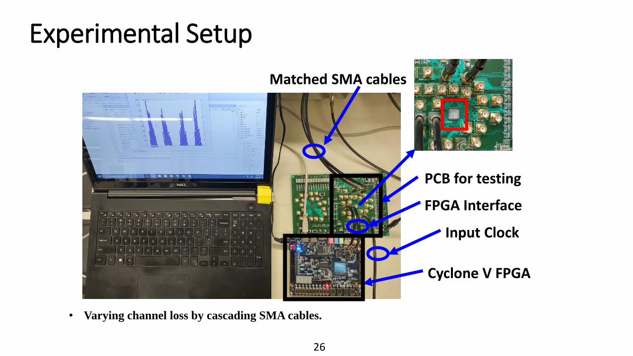
PCB for testing
Cyclone V FPGA
Matched SMA cables
Input Clock
FPGA Interface
26
• Varying channel loss by cascading SMA cables.
Experimental Setup

-0.5 -0.25 0 0.25 0.50
10
20
31
Time (UI)
AD
C C
od
e
-0.5 0 0.50
10
20
31
Time (UI)
AD
C C
od
e
27
Linear Equalizer
output EYE
Reconstructed digital
EYE from ADC output
frequency responses
of LR, MR and SR channelsSR
MR
LR
• Tx has 6 dB equalization
• Linear equalizer boost: 6 to 14 dB
Input EYE in Digital Domain

28
Equalized output code Equalized output code
BE
RO
ccu
rren
ce
-3 -1 1 3 -3 -1 1 3
3-tap LUT + 5-tap Conventional 8-tap Conventional
• FPGA gives the distribution of the bins
• The distribution is converted into log-scale
• Gaussian fit to extract the BER.
Link Margin at 28Gb/s 30 dB Channel

5.7 pJ/bit
4.6 pJ/bit
3.25 pJ/bit
2.1 pJ/bit2.1 pJ/bit
ADC
TDC
FFE
Channel Loss (dB)
Po
wer
(m
W)
@ 2
8 G
b/s
29
BE
R
• Receiver can achieve BER up to 10-9
Data rate: 28 Gb/s PAM-4
Link Margin Test and Energy Efficiency

30
Shafik
ISSCC 2015[4]
Frans
VLSI 2016[5]
Cui
ISSCC 2016[3]
Rylov ISSCC
2016 [6]
This Work
Technology 65 nm CMOS 16 nm FinFET 28 nm CMOS 32 nm CMOS 65 nm CMOS
Data Rate
(Gb/s)
10
NRZ
56
PAM-4
32
PAM-4
25
NRZ
28
PAM-4
ADC
Architecture
32x TI SAR
ADC
32x TI SAR
ADC
32x TI SAR
ADC
4x Flash ADC 4x Flash ADC
ENOB@
Nyquist
4.74 4.9 5.85 4 4.1
Timing
Recovery
N/A Baud-rate Baud-rate Baud-rate Edge & Data Sampled
Tracking BW --- --- --- --- 10+ MHz
Jitter
Tolerance
--- ---- --- --- 0.2 UIpp @ 50 MHz
Channel Loss
Equalization
36.4 dB
@ 5 GHz
25 dB
@ 14 GHz
32 dB
@ 8 GHz
40 dB
@ 12 GHz
30 dB
@ 7 GHz
Power (mW) 79(w/o DSP)
87(w DSP)
410(w/o DSP) 320 453 130@30 dB w/o
45 @ 15 dB DSP
160@30 dB with
60 @ 15 dB DSP
FOM (pJ/bit) 8.7 7.32 10 18.12 5.71@ 30 dB with
2.14@ 15 dB DSP
Comparison with state-of-art

• ADC- DSP Based receivers are the future for multilevel signaling in advanced CMOS – but it’s power has to be reduced.
• DSP needs to be more information efficient – Non-uniform quantization is a simple way to improve effective resolution.
• ADC for wireline is different than general purpose ADC. General purpose ADC considers each sample ‘uncorrelated’ but in reality channel ISI makes them ‘correlated’ – predictive ADC is a simple way to take advantage of that.
• Timing recovery is as important as data recovery – Multibit TDC and lower latency is an effective way to improve timing recovery loop and meet jitter requirement of the ADC.
31
Conclusion
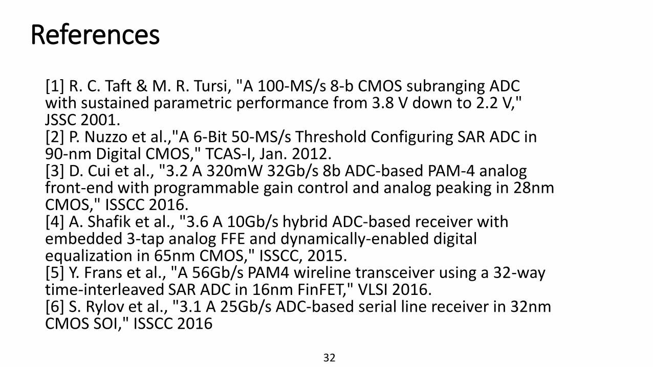
[1] R. C. Taft & M. R. Tursi, "A 100-MS/s 8-b CMOS subranging ADCwith sustained parametric performance from 3.8 V down to 2.2 V,"JSSC 2001.[2] P. Nuzzo et al.,"A 6-Bit 50-MS/s Threshold Configuring SAR ADC in90-nm Digital CMOS," TCAS-I, Jan. 2012.[3] D. Cui et al., "3.2 A 320mW 32Gb/s 8b ADC-based PAM-4 analogfront-end with programmable gain control and analog peaking in 28nmCMOS," ISSCC 2016.[4] A. Shafik et al., "3.6 A 10Gb/s hybrid ADC-based receiver withembedded 3-tap analog FFE and dynamically-enabled digitalequalization in 65nm CMOS," ISSCC, 2015.[5] Y. Frans et al., "A 56Gb/s PAM4 wireline transceiver using a 32-waytime-interleaved SAR ADC in 16nm FinFET," VLSI 2016.[6] S. Rylov et al., "3.1 A 25Gb/s ADC-based serial line receiver in 32nmCMOS SOI," ISSCC 2016
32
References

P315
P0
Φ0
Φ180
Edge SH
Edge Comp
Data SH for coarse
Data Comp
P0 EVEN Even Data SH for fine
P0 ODD Odd Data SH for fine
Φ90 EVEN
2UI 3UI
Edge comp. decision time
+ ref. update for coarse comp.Coarse comp. decision time + 3-bit code gen.
+ ref. update for fine comp.
Fine EVEN Comp
Fine ODD CompΦ90 ODD
3UI
Data Comp
33
Variable Resolution ADC – Timing Diagram

Edge Clk,
Φ0
Coarse Clk,
Φ180
Coarse Ref. Switching
Edge Comp.
SR O/P
Edge Comp.
S-ARM O/P
Coarse Reference Settling
34

C
CCp
Vp
Vn
Vp
Vn
P
P
C
R-Ladder and Reference Passing
35
t

36• ~50 ps timing margin for Reference passing
Coarse Reference
Fine Reference
Coarse & Fine – Reference Settling
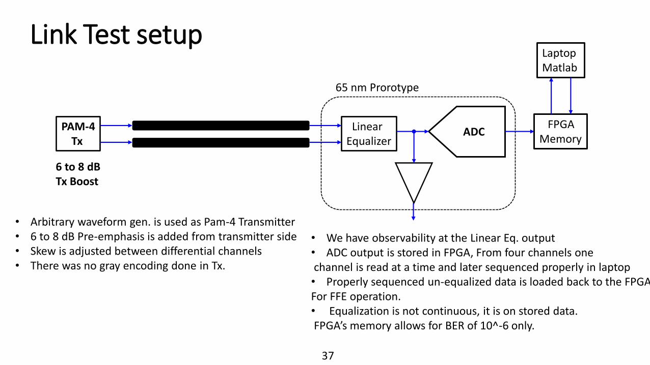
PAM-4Tx
6 to 8 dBTx Boost
Linear Equalizer
ADCFPGA
Memory
Laptop Matlab
65 nm Prorotype
• Arbitrary waveform gen. is used as Pam-4 Transmitter• 6 to 8 dB Pre-emphasis is added from transmitter side• Skew is adjusted between differential channels• There was no gray encoding done in Tx.
• We have observability at the Linear Eq. output • ADC output is stored in FPGA, From four channels one channel is read at a time and later sequenced properly in laptop• Properly sequenced un-equalized data is loaded back to the FPGAFor FFE operation.• Equalization is not continuous, it is on stored data. FPGA’s memory allows for BER of 10^-6 only.
37
Link Test setup

PAM-4Tx
6 to 8 dBTx Boost
Linear Equalizer
ADCIn 2 bitMode
65 nm Prorotype
• Arbitrary waveform gen. is used as Pam-4 Transmitter• 6 to 8 dB Pre-emphasis is added from transmitter side• Skew is adjusted between differential channels• There was no gray encoding done in Tx.
• We have observability at the Linear Eq. output • ADC output is stored in FPGA, From four channels one channel is read at a time and later sequenced properly in laptop• Properly sequenced un-equalized data is loaded back to the FPGAFor FFE operation.• Equalization is not continuous, it is on stored data. FPGA’s memory allows for BER of 10^-6 only.
SJ Mod.
MSB DAC
LSB DAC
Pattern Checker
Nearly loss lesschannel
38
JTOL Test setup

0 1 2 3 4 5 6 7
-60
-40
-20
0Fin: 458 MHz, ENOB= 5
Analgo Input Frequency (GHz)
Ma
gn
itu
de
(dB
)
39
0 1 2 3 4 5 6 7
-60
-40
-20
0Fin: 1.12 GHz, ENOB= 4.8
Analgo Input Frequency (GHz)
Magn
itu
de
(dB
)
FFT plot (W/ Offset Correction) Fs= 14 GHz

0 1 2 3 4 5 6 7
-60
-40
-20
0Fin: 5.67 GHz, ENOB= 4.3
Analgo Input Frequency (GHz)
Ma
gn
itu
de
(dB
)
40
0 1 2 3 4 5 6 7
-60
-40
-20
0Fin: 6.76 GHz, ENOB= 4.1
Analgo Input Frequency (GHz)
Magn
itu
de
(dB
)
FFT plot (W/ Offset Correction) Fs= 14 GHz

1UI
3
2222Pr
2Pr
22
,
PostQPostMainQMaineeQ
FFEQZoutQZ
WNWNWNhNN
-3
-1
+1
+3
41
postmainpre
XX
hhh
hW
PostMainex ,,Pr,
Effect of Quantization Noise in Conventional FFE

-3
-1
+1
+3
42
Margin Improvement

43
Two tone test• Apply two inputs: one is low frequency and another is high frequency.• Calculate the total input power by summing the two input power and calculate the SNDR. • Keep the low frequency signal unchanged, change the high frequency tone
ADC in High Frequency Input Test
0
Frequency
FFT
Mag
. (d
B)
-70

46
810
46
810
50
100
150
No. of taps
Power for different no. of taps and tap resolution
Tap resolution
46
810
46
810
50
100
150
No. of taps
Power for different no. of taps and tap resolution - LT
Tap resolution
3-tap LUT + 5-tap Conventional8-tap Conventional
44
Power Comparison – Digital FFE
• 8-tap with each tap resolution is 4-bit

Power vs. Resolution for different architecture
45