chapter 1 review of laser-matter interaction - csic · review of laser-matter interaction in this...
TRANSCRIPT

17
Chapter 1
Review of laser-matter interaction
In this chapter, an introduction to the fundamental interaction processes between light and matter is given, the case of semiconductors being specially considered. Starting with the optical properties of a material in a non-excited state, absorption, heating, melting, cooling, solidification, structural relaxation processes and their dynamics will briefly be described. The mathematical treatment of light-matter interaction can be done either by a classical or a quantum approach. In the following, I mostly restrict myself to the classical description. The formulae provided are only those which are fundamental for the understanding of the physics discussed or which will be used in the forthcoming results. A list of the symbols used in the equations is given at the end of this work.
1.1 Optical properties of matter In this section I will describe the interaction of electromagnetic radiation with matter and
how this interaction affects the optical properties of the material. The main interest will be focused on the visible part of the spectrum (380 - 780 nm, 3.3 - 1.6 eV, ∼ 1015 Hz). The electromagnetic radiation can interact only with the electrons of the atoms of the material because the much heavier nuclei are not able to follow the high frequencies of visible radiation. While core electrons have binding energies usually far higher than those provided by visible light and binding electrons interact only weakly with the electromagnetic wave below resonance, free electrons are accelerated and can absorb energy. This energy is then either re-emitted or transferred to the lattice.

Chapter 1: Review of laser-matter interaction
18
The optical properties of an isotropic material with characteristic configuration lengths much shorter than the wavelength of light can be described macroscopically. Upon illumination, the oscillating electrons generate their own electric field, i.e. they produce a polarization
vP of the
material. This field is superimposed to the incident field vE and the ratio between both can be
seen as the material response: r rP E= ε ω ε( ) 0 (1.1.)
where ε(ω) = ε1 + iε2 is the complex dielectric function that can be transformed into the complex refractive index nc(ω) = n + ik [Bor65].
n =+ +ε ε ε1
212
22
and k =− + +ε ε ε1
212
22
(1.2.)
where n and k denote the refractive index and the extinction coefficient, respectively. For normal incidence of light, the reflectivity of a material is defined as the incident to reflected intensity ratio and can be expressed as
Rn kn k⊥ =
− ++ +
( )( )
11
2 2
2 2 (1.3.)
For absorbing media only (k ≠ 0), the intensity of the electromagnetic wave propagating into the material decreases exponentially following the Lambert-Beer expression, where the absorption coefficient α is the inverse of the absorption length.
I z I e z( ) = ⋅ − ⋅0
α with απλ
=4 k
(1.4.)
The common classification of materials in metals, semiconductors and insulators is done according to their band structure. Ideal semiconductors and insulators in absence of excitation have only bound electrons, i.e. the conduction band is empty. Consequently, they are transparent*, except in the vicinity of resonances of the electrons with the electric field†. For semiconductors, the classical Lorentz model applies which describes binding electrons as damped
* For semiconductors, ambient temperature already generates a certain amount of free carriers which is
responsible for their quite high reflectivity in the visible spectrum. This will be discussed in detail later on.
† It is worth to remember that almost in all cases, the effects produced by the EM irradiation are caused by the electric component of the electromagnetic field rather than the magnetic component, which is neglectible. This becomes clear having a look at the force exerted by the electromagnetic wave on an electron, given by the Lorentz equation ( ) ( ){ }r r r r
F q E n c= − ⋅ + ⋅ ×v H . The contribution of the magnetic
field is smaller than that of the electric field by a factor of about v/c, where v stands for the electron velocity and generally holds v«c.
Chapter 1: Review of laser-matter interaction
19
harmonic oscillators within the material [Woo72], [Bon93]. In this model, the electrons experience the oscillating force of the electric field of the incident electromagnetic wave, given here in a plane-wave approximation.
r rE E e0
iz
t= ⋅
−
( )2π
λω
(1.5.)
The response of the material is described by the dielectric function ε(ω).
( )ε ω ωω ω ω
( ) = + ⋅− −
11
pci0
2 2 2Γ (1.
6.)
with ωεp
Nem
=2
0
being the plasma frequency (1.7.)
and Γc the damping constant describing the width of the resonance frequency ω0.
While in the classical model a resonance means that the frequency of the electric field is matched to the resonance frequency ω0 of the harmonic oscillator, a resonance in quantum mechanics corresponds to a transition between two states separated by the energy difference ∆E = ω0⋅h/2π . Additionally, a factor denominated oscillator strength has to be multiplied, taking into account the probability of the transition. These transitions can occur within one band (intraband) or between bands (interband). The most important resonances are found in the latter case where the incident photon energy must be at least equal to the band gap energy. While the wide band gaps of insulators usually require ultraviolet light for a transition to occur, transitions in semiconductors can be induced by visible or infrared light.
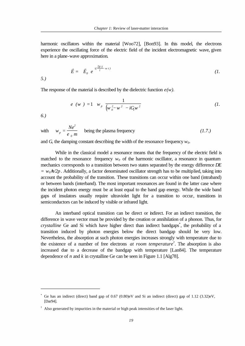
An interband optical transition can be direct or indirect. For an indirect transition, the difference in wave vector must be provided by the creation or annihilation of a phonon. Thus, for crystalline Ge and Si which have higher direct than indirect bandgaps*, the probability of a transition induced by photon energies below the direct bandgap should be very low. Nevertheless, the absorption at such photon energies increases strongly with temperature due to the existence of a number of free electrons at room temperature†. The absorption is also increased due to a decrease of the bandgap with temperature [Lan84]. The temperature dependence of n and k in crystalline Ge can be seen in Figure 1.1 [Alg78].
* Ge has an indirect (direct) band gap of 0.67 (0.80)eV and Si an indirect (direct) gap of 1.12 (3.32)eV,
[Dar94]. † Also generated by impurities in the material or high peak intensities of the laser light.

Chapter 1: Review of laser-matter interaction
20
Figure 1.1.: Temperature dependence of n and k in crystalline Ge for a photon energy of 1.96 eV (λ = 633 nm). Taken from reference [Alg78].
Nevertheless, for amorphous Ge or Si the absence of a perfect crystalline structure permits an infringement of the transition rules. An indirect transition can occur without compensating the wave vector by a phonon. Therefore, it may occur with a high probability thus increasing the absorption. In a-Si at room temperature and photon energies below the direct bandgap, the absorption is increased due to indirect transitions by a factor 10 compared to c-Si [Bro70], [Aic97].
The optical properties of the liquid state of semiconductors like Si and Ge can not be described by the Lorentz model. The solid-liquid phase transition liberates all four covalently bound electrons [Gla69], [Shv75] which causes the metallic behavior of the liquid [Jel87]. Metals are characterized by only partially filled bands. This implies a high density of free electrons and consequently a very short absorption length (1/α ≈ 10 nm) and a high reflectivity below the plasma frequency. The optical properties of metals and metal-like materials as liquid Ge can be described by the Drude model [Woo72], derived from the Lorentz model. Since the optical response is dominated by the free electrons which have no resonant frequency*, ωo is set to zero in the Lorentz model leading to the following expression for the dielectric function.
( )ε ω ω ττω
ω τ( ) = + ⋅ − +
⋅ +1 12 2 2
p ee
e
i (1.8.)
At the plasma frequency ωp, both ε1 and n vanish and the optical properties change from large R and α (for ω < ωp) to small R and α (for ω > ωp). The plasma frequency for liquid Ge can be calculated from the data reported by Jellison et al. [Jel87] and turns out to be ωph/2π = 18eV, i.e. in the far-ultraviolet. Since this work deals only with light in the visible region, liquid Ge can be considered as a metal, i.e. highly reflecting and absorbing.
* Notice that the only resonant frequency of a free electron plasma is the plasma frequency.

Chapter 1: Review of laser-matter interaction
21
1.2 Light absorption and plasma formation In order to induce a structural transformation in a material by means of light, the
absorption mechanisms and dynamics have to be considered first. It is fundamental to remember that only the amount of energy absorbed by the material can contribute to processes like heating and melting. In semiconductors, the absorption of photons leads to the creation of electron-hole-pairs with a certain amount of kinetic energy. These "hot" carriers thermalize amongst each other forming a plasma. Once a common carrier temperature is reached, they transfer their kinetic energy to the lattice via recombination and phonon generation, leading to lattice heating and melting.
In semiconductors, free carriers are created in pairs in interband transitions and consist of an electron and the corresponding hole. Holes tend to be mobile and behave like electrons but with the opposite charge and contribute also to the absorption process. The total absorption coefficient is composed of the lattice absorption coefficient and the carrier absorption coefficient. The latter scales with the square of the wavelength [Fan67] making free carrier absorption especially relevant for infrared illumination. The initial creation of free carriers via electronic transitions raises the absorption causing a stronger heating. Upon heating even more carriers are produced reinforcing the absorption. This cascade-like effect is denominated thermal runaway and can be observed very well in the infrared where the lattice absorption is small [All87].
In addition to optically generated free carriers, thermal excitation plays also an important role. The equilibrium free-carrier density of a semiconductor at a certain temperature is related to the carrier absorption coefficient by an Arrhenius dependency [All87]. This means, that the absorption coefficient increases faster than exp1/T, becoming important for temperatures above several hundreds degrees. Besides, many semiconductors - like metals but unlike insulators - already have a significant free carrier concentration under normal conditions (generated optically by the ambient light or thermally at room temperature). As a consequence, free carriers contribute to the high reflectance of many semiconductors in the visible region.
To describe a real situation which takes into account the generation and losses of carriers due to diffusion and recombination, a differential equation [All87] has to be solved. This equation will not be quoted here but I want to mention two important features related to it.
1. The recombination lifetime introduced there is in itself a function of temperature and carrier density.
2. The most important recombination mechanism is usually Auger recombination in the course of which the energy is transferred to a third carrier and not to the lattice.
At very high carrier densities (N > 1017 cm–3), carrier-carrier collisions dominate over carrier-lattice collisions and carriers begin to behave collectively, i.e. they form a plasma. This has the effect that thermal equilibrium is reached among the carriers before equilibrium with the lattice is reached. Carriers and lattice have now different temperatures [Yof80]. The plasma acts as an

Chapter 1: Review of laser-matter interaction
22
independent system, absorbing light and exchanging energy with the lattice. The following table gives the energy balance of gains and losses of the plasma.
PLASMA
gains energy by loses energy by
a) interband absorption (hω /2π - Eg per pair)
b) free carrier absorption
c) for every recombination event (Eg per event) (for Auger dominant recombination)
d) carrier diffusion
e) phonon emission
f) direct recombination by photon emission
Since only process e) heats the lattice, the plasma can be considered as a funnel through which the absorbed energy has to go before it is transferred to the lattice. There is a differential expression [Lie82] to calculate the resulting average excess carrier energy, but the main difficulty is that the material parameters depend on the temperatures of the plasma and the lattice as well as on the plasma density. For a degenerated plasma, i.e. when the carrier density is not small any more compared to the density of states and thus the carrier distribution deviates from a Boltzmann distribution, the diffusion of hot carriers out of the light-absorbing zone increases strongly [Yof80]. As a consequence, the absorbed laser energy is not defined any more by the exponential light absorption profile but by the diffusion length of those carriers.
At very high intensities of the laser pulse (> 106 W/cm2), evaporation and plasma effects become important. These processes are highly complex and the following paragraph is only a brief survey of some phenomena occurring under these conditions. Even in the regime in which no ablation takes place, vapor clouds with a different and inhomogeneous refractive index may distort the incident wavefront. The distance of the vapor plasma from the surface plays also an important role. If it stays close to the surface, absorption by the solid through the plasma is much more efficient than by laser irradiation (especially for infrared lasers) since the blackbody radiation emitted by the vapor plasma is absorbed very strongly [All87]. For even higher intensities, ionization of the vapor takes place and the breakdown plasma propagates against the incident beam, shielding the material completely. At extremely high intensities (> 109 W/cm2), the plasma becomes transparent, light is again transmitted to the material and the ablation pressure drives a shock wave into the material altering the structure and optical properties within broad regions of the material [All87].

Chapter 1: Review of laser-matter interaction
23
1.3 Heating As shown in the previous section 1.2, the light absorbed is not directly converted into
heat, but into excess energy distributed between the excitation energy for the bound electrons, the kinetic energy of free carriers and the excess of phonons. The transformation of this energy into heat takes place in three steps [Aga84], [Sok95], [Gol94]:
1. Spatial and temporal randomization of the motion of the particles by collisions in the femtosecond time scale, until they reach a thermal equilibrium.
2. Energy transfer to the lattice involving a large number of mechanisms, each of them with its own time constant. They can be described by an overall energy relaxation time depending on the material and the laser intensity. The typical order of magnitude in most materials is a few picoseconds.
3. Heat flow towards cooler regions*, given by the equation (in one dimension) [All87]
∂∂
∂∂
∂∂z
Tz
Tt
( ) ( ) ( )Kc
Vp
⋅ = ⋅ (1.9.)
If heat is produced by absorption within the material, the power density of the heat source has then to be added to the left hand side of equation (1.9). For an analytical solution, important simplifications have to be made. All material parameters are assumed to be constant, the material is assumed to be a homogeneous and thermally insulated slab, and the power density of heat production is set equal to that of the absorbed light. Generally, the Green’s function technique is applied to describe the temperature distribution of an instantaneous heat source. It would go beyond the purpose of the present chapter to follow the whole calculation but there is a simple approximation from the heat flow equation for the surface temperature following the absorption of a laser pulse with a fluence F (energy/ area) illuminating a sample of thickness d [All87]. We assume that heat is produced due to absorption over a length 1/α and diffuses during the pulse duration tp over a length Lth:
L tth p= ⋅2 κ , if d < Lth, replace Lth by d (1.10.)
where κ denotes the thermal diffusivity of the film.
* The heat flow towards the air compared to the heat flow into depth is neglectible due to the extremely
low thermal diffusivity of air. For instance, the relation of the heat flow towards the air and towards such a bad heat conductor as glass is jair/jglass ≈ 0.1%. The energy loss of a material at the melting temperature due to heat radiation following the Stefan-Boltzmann law [Bec75] is about 3 orders of magnitude smaller than the heat flow towards the substrate. Both can be calculated exactly, see for instance [Sku95].

Chapter 1: Review of laser-matter interaction
24
Then, the surface temperature at the end of the laser pulse is approximately given by:
T z t F Rt
cp
p
p
( , ) ( )= ≅ ⋅ ⋅ − ⋅0 1.13 1κ
ρ , for 1/α « Lth (1.11.)
T z t F Rcp
p
( , ) ( )= ≅ ⋅ ⋅ − ⋅0 1αρ
1 , for 1/α » Lth (1.12.)
While in both cases one has to take into account the temperature dependence of R and cp, in the latter also the temperature dependence of α turns up. If α is small but increasing with temperature, a controlled heating is impossible (positive feedback).
Some very illustrative calculations of temperature distributions taken from Ref. [All87] are given in the following. Figure 1.2 shows the normalized temperature distributions in a semi-infinite solid for a uniform heat source as a function of normalized depth.
normalized depth (z/Lth)
Figure 1.2.: Normalized temperature distributions for uniform heat sources as a function of normalized depth. Numbers indicate the ratio of the absorption length 1/α to the diffusion length Lth. Taken from reference [All87].

Chapter 1: Review of laser-matter interaction
25
The analysis of the two extreme cases of an absorption length being zero or equal to the thermal diffusion length reveals the drastic differences between the resulting temperature profiles. In the former case the exponential absorption profile is resembled by an entirely exponential temperature profile with an extremely high surface temperature (no heat flow during the pulse duration). In the latter case a gaussian temperature profile with a low surface temperature is induced due to heat conduction into the bulk, which minimizes the temperature gradients.
Another illustrative calculation is given in Figure 1.3 showing the evolution of the normalized temperature with time for various depth for a temporally rectangular laser pulse. The maximum temperature at a certain depths occurs later for larger depths. For very large depths only very low maximal temperatures can be reached which are approximately constant for a long time.
Figure 1.3.: Normalized temperature as a function of normalized time t/tp at various depths for a rectangular temporal shape. Numbers indicate the ratio of the actual depth to the diffusion length Lth during the pulse duration. Taken from reference [All87].

Chapter 1: Review of laser-matter interaction
26
1.4 Melting Laser induced heating of a material does not necessarily involve melting. Nevertheless, a
much wider field of material modification becomes accessible upon melting followed by rapid solidification. This is mainly due to the unique properties of melts, such as high atomic mobility and solubility which enables structures that are not accessible through pure solid-state reactions. For example, nearly perfect doped crystals, complex structured alloys and amorphous materials can be produced by laser irradiation involving melting followed by rapid solidification [Poa82], [All87].
Doping crystals is usually done by ion-implantation which causes large disorder in the crystalline structure of the upper layer turning it amorphous. Furnace annealing or rapid thermal annealing is usually performed to recover crystallinity, the amorphous material crystallizing directly in the solid state. Under laser irradiation with short pulses [Kac75], [Poa82] crystals of a better quality are obtained in a much shorter time, due to the fact that regrowth occurred from a melt in which the atoms are much more mobile.
Surface alloying can be done by laser irradiation of a multilayer system where the several layers of different materials are subsequently melted, mixed and rapidly solidified. This technique has the huge advantage towards bulk alloying that it permits considerable material savings of scarce alloying materials. In addition, the fact that the processes occur far from the thermodynamic equilibrium makes the resulting alloys to belong to a class of materials with new properties.
Materials which have been thought not to be glass formers can be transformed to their amorphous or glassy state* by means of laser irradiation [Liu79]. This can be done by ultrarapid solidification following laser melting which is often referred to as laser quenching. Irradiation with nanosecond pulses can lead to cooling rates exceeding 1010 K/s [Sti91], many orders of magnitude faster than conventional mechanical methods like melt spinning. The cooling rates depend on the pulse duration and the thermal conductivity of the solid material in contact with the liquid [All87].
The role of latent heat
When melting occurs during laser induced heating, it is necessary to take into account the latent heat. In order to melt a material, not only the energy to reach the melt threshold has to be provided by the laser pulse but also the latent heat, denominated also melt enthalpy. The amount of heat necessary to preserve melting depends strongly on the material and is proportional to the
* see Appendix A.2 for details on cooling rates and glass formation.

Chapter 1: Review of laser-matter interaction
27
volume to be melted. The relation between the energy required to reach the melting point* ∆H→Tsl and the melt enthalpy ∆Hsl is very important in order to understand the material behavior during melting followed by rapid solidification. A look at these quantities listed in the book by von Allmen [All87] (partly shown in Table 1.1) indicates a clear difference between metals and semiconductors. Whereas the relation ∆Hsl/∆H→Tsl for semiconductors is generally higher than 1, for metals it is much smaller than 1. As a consequence of the high ∆Hsl values, it is “more difficult” to melt a semiconductor lattice than a metal lattice. Taking into account that during solidification (the “inverse” process of melting) ∆Hsl is released, semiconductors are also expected to solidify slower than metals. Semimetals as Antimony (Sb), which is also included in the table, present values of the relation ∆Hsl/∆H→Tsl similar to those of semiconductors.
Material
Tsl (K)
∆H→Tsl (kJ/mole)
∆Hsl (kJ/mole)
∆Hsl _ _ _ _ _ _ _ _ _ _ _ _ _ _ _ _ _ _ _ _ _ _ _ _ _ _ _ _ _ _ _ _ _ _ _ _ _ _
∆H→Tsl
Ge 1210 25.8 34.8 1.35
Si 1685 36.0 50.3 1.39
Sb 904 16.6 20.1 1.20
Ag 1234 23.3 12.0 0.52
Co 1768 54.0 15.9 0.29
Al 933 17.2 10.7 0.62
Table 1.1.: Thermodynamic data of selected semiconductors, semimetals and metals. ∆H→Tsl is the heat required to reach the melting point Tsl starting from the room temperature, ∆Hsl the latent heat for melting. Data taken from reference [All87].
This feature of high latent heat values in combination with a related phenomena - the high reflectivity of some liquid semiconductors in the visible - can lead to a very peculiar phenomenon, known as “melting instability”. This effect occurs under irradiation by visible or infrared laser pulses with durations clearly longer than the time required to melt the material. In Si or Ge irradiated just above the melt threshold, it has been found [Haw83] that the power absorbed by the solid is sufficient to initially melt the surface, but the power absorbed by the initially formed liquid is insufficient to prevent resolidification. Hence, neither a homogeneous solid nor a homogeneous melt are stable and a mixture of solid and molten patches coexist at the surface. The ratio of molten to solid fraction is a function of pulse energy, while the feature size is determined by the optical absorption length in the solid [Com84].
* starting from the room temperature.

Chapter 1: Review of laser-matter interaction
28
Dynamics of Melting
The absorption, heating and melting processes induced by ultrashort laser pulses occur in very short time scales as can be seen in Figure 1.4. The photons absorbed by the valence band electrons create* a dense population of electron-hole pairs which thermalize within tens of femtoseconds via carrier-carrier scattering [Aga84], [Yof80], [Elc77], [Sok95], [Gol84]. Having reached a common temperature, they start to equilibrate with the cold lattice by electron-lattice collisions (phonon generation) accompanied by electron-hole relaxation via Auger process [Yof80] and inward spatial diffusion of carriers, due to carrier-density and temperature gradients [Sha83]. Agassi [Aga84] provides a phenomenological model which is able to calculate the electron-phonon relaxation constant t0, during lattice heating. He predicts t0 to be in the order of 0.4-1 ps for the case of ps pulse irradiation (20 ps) of Si and Ge. This is in agreement with the recent work of Sokolowski-Tinten et al. [Sok95] who found experimental values for the relaxation constant of 1-2 ps.
Figure 1.4.: Schematic diagram of the electronic excitations and of the energy transfer to the lattice upon intense laser irradiation. a, b, c correspond to the laser induced excitations. The remaining transitions represent the thermalization processes which finally lead to the energy transfer to the lattice. An analogous diagram holds for holes. Taken from reference [All87].
At moderate carrier injection rates (i.e. for sufficiently long pulses or moderate peak powers), the electronic system and the lattice can be considered to be permanently in equilibrium and thus the melting process can be considered “thermal”. In this case nucleation of the melt occurs heterogeneously at the surface of the solid material [Jel86], [Sol92b]. Following nucleation, a melt front forms which may propagate at extremely high velocities into the solid, with the upper limit being the speed of sound. For example it takes between 50 and 100 ps to melt a 20 nm surface layer of a Si wafer, providing melt-in interface velocities of 100 to 200 m/s [Dan88].
* at a rate of ∼1030 s -1 for laser intensities of 108 W/cm2 [Whi80].
Chapter 1: Review of laser-matter interaction
29
At this point it is necessary to have a closer look to the influence of the pulse duration on the dynamics of the melting process. Already in 1986, Nicholas Blombergen [Blo86] pointed out that even pulses as short as tens of picoseconds act essentially as a very fast heating source inducing thermal melting as observed for ns pulses. The extremely high heating rates of 1014 K/s attainable with ps pulses can lead however to superheating* of the solid by many hundreds of degrees as observed in GaAs by Fabricius and coworkers using 25 ps laser pulses [Fab86].
The prediction of Blombergen has its physical basis in the fact that the characteristic phonon emission time in most solids is below or in the order of a few picoseconds† [Sae91]. The thermal model assumes that the excess energy of photoexcited carriers relaxes rapidly to lattice vibrational modes, predominantly by the emission of longitudinal optical (LO) phonons [Dri87]. The phonon emission time is therefore the time required for a hot electron to emit a single LO phonon and consequently a measure for the time required to thermally heat the material. However, if the pulse duration is below the phonon emission time and the pulse peak power is sufficiently high, a huge amount of carriers can be excited from bonding to antibonding states leading to the softening of the lattice in a completely non-thermal process. Such a lattice softening has been proposed first by van Vechten et al. [Vec79] in the 80’s in order to explain the results of ns laser pulse annealing of semiconductors. This model predicted correctly that Si should melt non-thermally for free carrier densities above 1021 cm-3, but incorrectly that this could occur under ns pulse irradiation‡.
The improvement of ultrashort dye laser pulse technology carried out in the early 80’s made it possible to confirm the initial prediction of Van Vechten. For the first time in 1983, Shank and coworkers [Sha83], [Sha83b] demonstrated that upon irradiation of Si with intense 90 fs laser pulses a metastable excited state of the material is generated which lasts a few hundred femtoseconds before the molten phase of the material appears. The additional work of Tom [Tom88], Govorkov [Gov92], Sokolowski-Tinten [Sok95] and Shumay [Shu96] in tetrahedral
* The term "superheating" refers to the heating of a material up to a temperature above its equilibrium
melting point before melting takes place. Nevertheless, there exists a limiting superheating value for any crystalline structure [Bor62], [Wol92], [Lam94]. At a certain critical volume expansion, an elastic instability in the minimal shear constant turns up and the crystal becomes mechanically unstable forcing it to perform a phase transformation. This temperature, where the material melts continuously without prior nucleation of the melt is usually denominated mechanical melting point.
† Kash and coworkers measured the rate of LO phonon emission in GaAs finding a value for the phonon emission time of 165 fs [Kas85]. This value corresponds to low carrier densities. At densities above 5*1017 cm-3, screening lowers the emission rate [Yof81]. Hot phonon effects may also lower the emission rate [Sha85]. Hence, the 165-fs emission time represents a limit of the rate of energy relaxation to the lattice.
‡ The “plasma annealing hypothesis ” by Van Vechten [Vec79] was meant to explain the solid-state crystallization of amorphous Si. His hypothesis was based on the formation of a long lasting solid-state plasma at fluences below the melt threshold which enabled the recovery of the covalent crystal structure once the energy has been transferred to the lattice. The interpretation of Van Vechten has nevertheless been disproved by several time-resolved experiments (e.g. [Aus79]) which prove that the high reflectivity state observed in Si, Ge and GaAs was actually the molten phase and not a long-living plasma.

Chapter 1: Review of laser-matter interaction
30
semiconductors, allowed to prove that the metastable phase is liquid and that non-thermal (“cold”) melting of the lattice may be induced via carrier excitation by pulses shorter than the characteristic phonon emission time. Once the non-thermal liquid phase is formed at the surface, the material may remain in this highly excited metastable state for several hundreds of fs before the transition to the thermodynamic liquid phase occurs*.
In fact, femtosecond laser pulses may produce both, thermal melting (as ns and ps pulses) or ultrafast non-thermal melting depending on the pulse fluence. This was demonstrated experimentally by Sokolowski-Tinten and coworkers [Sok91] who found that the transformation of GaAs into its liquid state occurs within several tens of picoseconds at fluences close to the melt threshold due to thermal melting under highly superheated conditions [Sok91] or within several hundreds of femtoseconds via carrier excitation [Sok91], [Sok95] for very high fluences. The processes occurring under high energetic fs pulse irradiation could be described more precisely with the help of the theoretical work of Stampfli et al. [Sta94], [Sta95]. Based on a dynamic theory with a tight-binding formalism, the authors found that the lattice is not only softened by the removal of binding electrons but also by the dense electron-hole plasma which causes a displacement of the atoms. They calculated that a displacement of the atoms of more than 1 Å from their equilibrium position occurs within less than 200 fs after the laser pulse. The gap between the conduction and the valence bands then vanishes and the symmetry of the diamond structure is destroyed. This has an important effect on the optical reflectivity which is expected to correspond to that of a metal.
Notice however that the distinction by optical techniques between the non-thermal liquid and the final thermodynamic metallic liquid is problematic due to the fact that the properties of the non-thermal liquid are qualitatively similar to those of a metal. Structural transitions occurring in the material may be screened by laser-induced changes of the linear and non-linear optical properties, as suggested by several authors [Tom88], [Sae91], [Sok91]. Sokolowski-Tinten and coworkers [Sok95] provided more detailed experimental data in this aspect measuring the optical reflectivity and SHG† of Si and GaAs. As a consequence they were able to establish a two-step model of the laser induced structural transformation. First, the “excitation stage” within the first 100 fs where the linear and non-linear optical properties of the material are determined mainly by electronic excitation mechanisms and barely by disordering. Secondly, the subsequent “transition stage” in which the non-thermal liquid phase is transformed into the thermodynamic metallic liquid within 300 fs at high fluences (three times the melt threshold).
1.5 Solidification
* The occurrence of electronic excitation induced crystallization of an amorphous phase within several
hundreds of fs has been recently reported by Solis and coworkers [Sol96c], [Sok98]. † Second Harmonic Generation (SHG) provides information about the material structure because it
measures the non-linear susceptibility tensor which is a measure for the lattice symmetry [Tom83].

Chapter 1: Review of laser-matter interaction
31
In this section we assume a situation in which a laser pulse of sufficient energy has melted a layer of a certain thickness of the semiconductor material. In order to solidify this liquid layer, first of all, nuclei of the solid material (amorphous or crystalline) have to be formed. There are several different types of nucleation scenarios which may take place depending on the heat flow conditions defined by the system and the laser pulse. Once stable solid nuclei are formed within the liquid phase, they are able to grow in different manners until the whole material is solidified. The re-solidified material is still at elevated temperature and the cooling process down to ambient temperature is very slow compared to the solidification process and it is usually accompanied by no further structural transformation.
Thermodynamics
In order to follow both the nucleation and solidification process of a material, it is necessary to consider its thermodynamic properties. The Gibbs free energy G of a system composed of only one element in one phase is defined as:
G H TS= − (1.13.)
H and S being the enthalpy and entropy, respectively. The equilibrium melting temperature Tsl is the temperature at which the liquid and the solid have equal free energies G. Any deviation from Tsl causes one phase to become unstable. The resulting difference in the Gibbs free energy ∆G can be expressed approximately by [All87]:
∆ ∆ ∆ ∆∆
G H T S HT
Tsl
= − ≈ ⋅ (1.14.)
which is the chemical driving force for the motion of a solid-liquid interface [All87]. Here, ∆H is the latent heat and ∆T = Tsl -T is the undercooling*. Notice that ∆G is negative at the undercooled molten interface.
* We use the term “undercooling” to refer to the temperature deviation of an interface from the melting
temperature and the term “supercooling” to refer to the temperature deviation of a bulk liquid from the melting temperature following the criterion defined in reference [Sti88]. Nevertheless, the reader should keep in mind that in most of the works the difference between both situations is unfortunately not expressed correctly using for both cases the term undercooling.

Chapter 1: Review of laser-matter interaction
32
Nucleation
In the following, the classical nucleation theory in its simplest form will be introduced as first done by Volmer and Weber in 1926 [Vol26]. It requires two important approximations: First, the properties of small clusters are approximated by the bulk material properties and secondly, the model is limited to spherical clusters. The consequences and limitations of these approximations can be found for instance in the book by Christian [Chr75]. The theory of homogeneous nucleation of the solid phase within a liquid is based on the assumption that solid clusters form at an undercooled interface (or in an supercooled melt) by way of density fluctuations. The atoms in the melt have kinetic energies around a mean value given by the temperature of the melt. This kinetic energy distribution leads to density fluctuations in the system which are generally compensated after a short time, defined by the diffusion velocity. Assuming the clusters to be spherical with a radius r, the local change of the free energy ∆G at the cluster site is then given by [Jen92], [Kur86]:
∆ ∆G r r gsl= +443
2 3π γπ
(1.15.)
Here, the two components are given by the solid/liquid interface energy γsl and the Gibbs free energy per unit volume ∆g the latter being mainly the difference between the chemical potentials of the two phases which is proportional to the undercooling [Sei56]. Figure 1.5 shows a plot of this equation for the two cases of ∆g positive (T > Tsl) or negative (T < Tsl).
For a positive ∆g, the free energy of the cluster increases with r3, i.e. the cluster dissolves. For a negative ∆g, the contribution by ∆g decreases with r3 but the amount of energy needed to preserve the surface still increases with r2. After reaching a maximum at the so-called critical radius rcr, ∆G decreases and the cluster becomes stable, i.e. it can not vanish any more due to fluctuations and may grow. The value of the free energy corresponding to rcr is called activation energy or nucleation barrier ∆Gcr.
rgcrsl= −
2γ∆
(1.16.)
∆∆
Ggcrsl= ⋅
163
3
2
π γ (1.17.)

Chapter 1: Review of laser-matter interaction
33
4π r γ24π r γ2
(4/3)π r ∆ g3
r r
∆G
0 0
∆G
(4/3)π r ∆g3∆g > 0 ∆g < 0
rcr
a) b)
Figure 1.5.: a) The change of the enthalpy ∆G increases with the cluster radius for a positive ∆g, thus dissolving the cluster. b) If ∆g is negative, ∆G decreases for radii bigger than a critical value rcr, and thus the cluster may grow. Taken from reference [Jen92].
The nucleation rate at which nuclei form depends strongly on temperature and increases threshold-like at the nucleation temperature Tn for small undercoolings/ supercoolings. For very large undercoolings/supercoolings, the decrease of the atomic diffusion causes measurable nucleation to occur only after a finite time-lag. Both processes are competing and thus the nucleation rate has a maximum at a certain temperature [Kas69], [Kel83].
The mechanism described above refers to homogeneous nucleation in which only the two phases of a single material are involved. Generally, heterogeneous nucleation is the more common process. This means that the presence of other “surfaces” as impurity particles or material boundaries (e.g. a film/substrate interface) promote nucleation. As a consequence, nucleation is found to occur at undercoolings much smaller than those predicted by the homogeneous nucleation theory. In addition, the nucleation rate can be controlled by impurities, mechanical vibrations or electric (magnetic) fields [Jen92]. In order to be able to describe such real systems, Turnbull [Tur50] extended the classical nucleation theory to three-component-systems. In such systems, the surface energies of the solid-substrate interface γssu and the liquid-substrate interface γlsu are taken into account in addition to the surface energy γsl of the solid liquid interface. This leads to the following expression for the heterogeneous nucleation barrier:
∆ ∆G G fcr het, ( )= ⋅cr, hom θ (1.18.)
where f(θ) is the heterogeneous nucleation factor which can be calculated from the surface energies. Since, f(θ) ≤ 1, the nucleation barrier is lowered and consequently the nucleation rate for a given temperature is increased upon heterogeneous nucleation. Unfortunately, quantitative predictions within this theory are difficult since the microscopic properties of the nucleation centers are in the most cases not known. At large driving forces once the nuclei are formed, homogeneous nucleation dominates over heterogeneous nucleation which, the latter occurring only at a limited number of nucleation centers.

Chapter 1: Review of laser-matter interaction
34
Apart from homogeneous and heterogeneous nucleation, there is a third possible mechanism. This mechanism has been found to occur during laser pulse induced explosive crystallization of amorphous semiconductors [Nar84], [Tho83], [Low86], and shows that nucleation occurs at a solid-liquid interface which moves with high velocity [Tsa87].
Growth of Clusters
Once the critical size is reached, clusters may grow. There are two types of growth that have to be distinguished [Poa82], heat flow limited and interface limited. While in the former case the growth velocity is determined by the diffusion of the released latent heat out of the supercooled melt, in the latter case the velocity is determined by the transport and incorporation of atoms into the lattice, the topology of the interface being crucial for the incorporation of atoms. It may contain different types of places like planes, steps, voids, gaps, etc. all with different energies. Usually, an adsorbed atom will incorporate at the site of lowest energy (γsl) [Kur86]. For a given material and undercooling, the velocities of both types of growth can be calculated [Poa82] and the smaller velocity determines the dominant type of growth and gives therefore the solidification velocity. For Si and Ge, the growth velocity of the crystal is determined by the incorporation of atoms into the lattice and therefore interface limited [Poa82]. These crystals grow in twin planes which permits to offer always low energy sites for adsorbed atoms to incorporate [Jen92].
A net movement of the liquid-solid (l-s) interface results from non-balanced melt. The solidification rates and the velocity of this movement can be expressed as:
u aB ej
GRT= ⋅ −ν ( )1∆
(1.19.)
where a is the interatomic spacing in the growth direction, νj is a thermally activated jump frequency and B is the accommodation probability for atoms in the growing phase. The latter can be interpreted as the fraction of boundary sites which are energetically favorable for atoms to attach, as discussed before. For metals, B is mostly close to unity, whereas for semiconductors it is small and anisotropic: Growth in Si along the close packed <100> direction is observed to be faster than along the <111> direction [Jac75], [Abr86].
For small undercoolings (∆G « RT) the following expression is obtained from equations 1.19 and 1.14:
u aBG
RTaB
H TRT Tj j
sl≈ − = −
⋅⋅
ν ν∆ ∆ ∆
(1.20.)
which means that the interface velocity in this case is approximately proportional to the undercooling. For very large undercoolings, the exponential term in equation 1.19 tends towards unity and the velocity becomes small and proportional to the jump frequency. There is an
Chapter 1: Review of laser-matter interaction
35
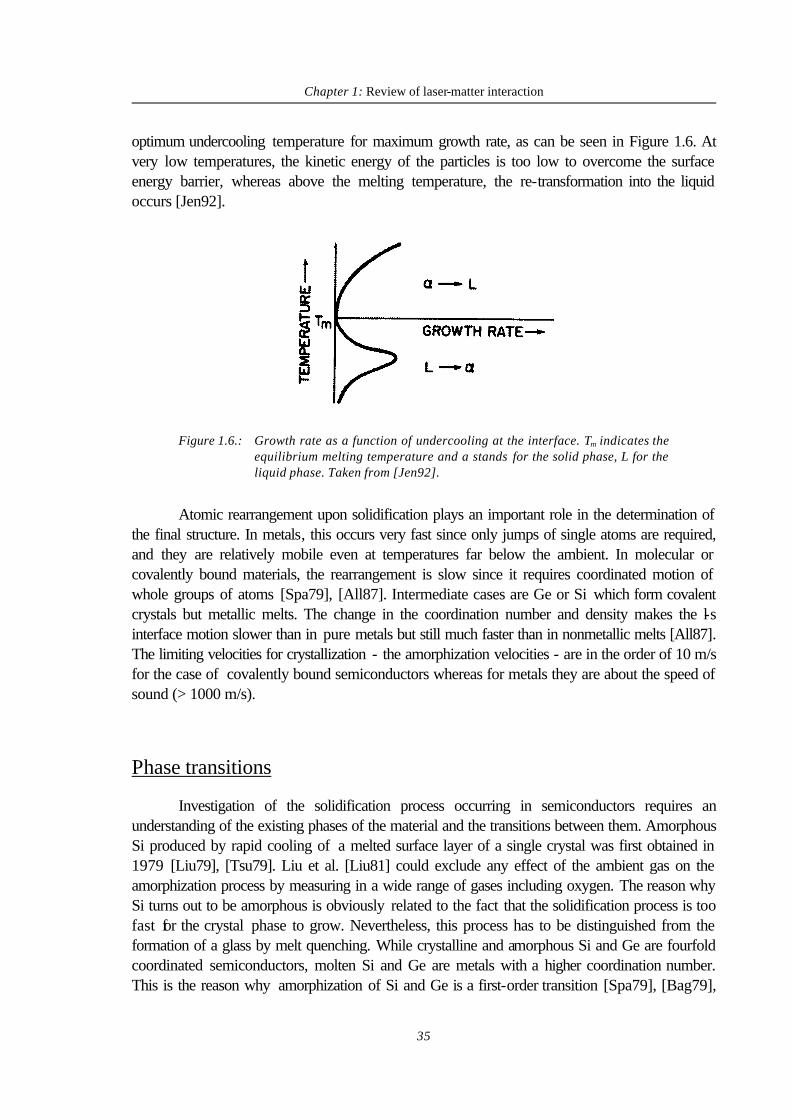
optimum undercooling temperature for maximum growth rate, as can be seen in Figure 1.6. At very low temperatures, the kinetic energy of the particles is too low to overcome the surface energy barrier, whereas above the melting temperature, the re-transformation into the liquid occurs [Jen92].
Figure 1.6.: Growth rate as a function of undercooling at the interface. Tm indicates the equilibrium melting temperature and a stands for the solid phase, L for the liquid phase. Taken from [Jen92].
Atomic rearrangement upon solidification plays an important role in the determination of the final structure. In metals, this occurs very fast since only jumps of single atoms are required, and they are relatively mobile even at temperatures far below the ambient. In molecular or covalently bound materials, the rearrangement is slow since it requires coordinated motion of whole groups of atoms [Spa79], [All87]. Intermediate cases are Ge or Si which form covalent crystals but metallic melts. The change in the coordination number and density makes the l-s interface motion slower than in pure metals but still much faster than in nonmetallic melts [All87]. The limiting velocities for crystallization - the amorphization velocities - are in the order of 10 m/s for the case of covalently bound semiconductors whereas for metals they are about the speed of sound (> 1000 m/s).
Phase transitions
Investigation of the solidification process occurring in semiconductors requires an understanding of the existing phases of the material and the transitions between them. Amorphous Si produced by rapid cooling of a melted surface layer of a single crystal was first obtained in 1979 [Liu79], [Tsu79]. Liu et al. [Liu81] could exclude any effect of the ambient gas on the amorphization process by measuring in a wide range of gases including oxygen. The reason why Si turns out to be amorphous is obviously related to the fact that the solidification process is too fast for the crystal phase to grow. Nevertheless, this process has to be distinguished from the formation of a glass by melt quenching. While crystalline and amorphous Si and Ge are fourfold coordinated semiconductors, molten Si and Ge are metals with a higher coordination number. This is the reason why amorphization of Si and Ge is a first-order transition [Spa79], [Bag79],

Chapter 1: Review of laser-matter interaction
36
whereas glass formation can be thought of as the freezing of a melt maintaining its structure which is considered a second-order phase transition [Tur81].
In order to understand the possible paths for phase transitions, I included in Figure 1.7 a schematic phase diagram reported for Si in Ref. [Woo84] showing the evolution of the temperature as a function of enthalpy. The one of Ge is very similar with the exception of the absolute values. A certain point on a line in this diagram corresponds to the state of the phase (a-Ge, c-Ge and l-Ge) in which the material is at that moment*. Following the line to intersection points with other lines corresponds to performing a phase transition as will be explained below.
l-l
ine
c-lin
ea-
line
mix-line
mix-line
Hlna
Ha
Hla
Hlnc
Hlc
Ta
Tn
Tc
Hc
Tem
pera
ture
T
Enthalpy H
Figure 1.7.: Phase diagram of Si relating temperature and enthalpy. The right plot is a
detail of the left figure and the solid (dashed) arrows indicate the possible heating (cooling) paths. Taken from reference [Woo84].
The horizontal lines correspond to mixed phases during a first order phase transition. During these transitions, the characteristic latent heats (Hla - Ha and Hlc - Hc) have to be either provided or released. Also, the difference in enthalpy (Ha - Hc) between the crystalline state of lower energy (thermodynamically stable) and the amorphous state of higher energy (metastable/unstable) can be appreciated in this figure. An important consequence of this enthalpy difference is that the amorphous material has a lower melting point than the crystalline material. This feature of a much lower melting temperature of the amorphous causes it to be immediately in a unstable, supercooled state if it is melted just above Ta.
* Even when in this plot the temperature dependence of ∆H for amorphous Si (Ge) is given by a line, it
should be thought of as a broad line or an area. This is due to the uncertainty in the thermodynamic data depending on the state of structural relaxation of the amorphous material [Don83]. Naturally, this implies also a range of melting temperatures Ta and enthalpies Ha and Hla. This dependence will be discussed in more detail in section 1.6.

Chapter 1: Review of laser-matter interaction
37
Let us consider now a situation in which a laser pulse heats the solid and summarize the several processes that may occur depending on the initial state of the material [Woo86]:
• Initially crystalline:
As the material heats up, the temperature and enthalpy increase along the c-line until the intersection point (Hc, Tc) is reached. The material undergoes melting along the mixed-line with the temperature remaining constant at Tc, while the melt enthalpy of the volume of material under consideration is absorbed. At the point (Hlc, Tc), the volume is melted completely and the temperature of the liquid begins to increase until the vaporization line is reached. If at some time the material is allowed to cool then the temperature falls until reaching (Hlc, Tc). If the cooling rate is slow enough, then there will be little undercooling and the system essentially will reverse its heating path and recrystallize. If the cooling rate is large enough and no solid material is near that could serve as a seed for nucleation of the crystalline phase, then the supercooling of the liquid increases until nucleation events occur by way of density fluctuations and crystallization takes place. The release of the crystallization heat induces a temperature increase of the solidifying material up to Tc. This corresponds to a transition in the state diagram from the corresponding point at Hlnc to the Hc - Hlc line at temperature Tc. If the cooling rate is even higher and no nucleation of the crystalline phase occurs, the supercooling increases and amorphous material nucleates [Sti90], [Sti91]. Therefore, the path in the state diagram for the case of amorphization would be as follows: The liquid is supercooled down to the point (Hlna, Tna) where the amorphous phase nucleates. The release of the amorphization heat (< crystallization heat) increases the temperature of the liquid which solidifies at a slightly higher temperature Ta. Depending on the dynamics of the amorphization process, a more or less relaxed state of the amorphous with its corresponding Ta and Ha values is obtained.
• Initially amorphous:
In this case the enthalpy and temperature increase along the a-line until (Ha, Ta) is reached. The amorphous begins then to melt along the Ha - Hla line with the temperature remaining constant. At Hla the material under consideration is fully molten but highly supercooled. If the temperature remains between Ta and Tn long enough for nucleation of the crystalline phase to occur, a transition to the Hlc - Hc line will be made as described in the preceding example. If the line segment Hla - Hlnc is traversed rapidly enough, nucleation of the crystalline phase may be prevented. For sufficiently high energy input from the laser and/or because of the release of latent heat, the liquid will be heated above Tc. On cooling, the several solidification paths as discussed in the preceding example take place leading to crystallization or amorphization, depending on the dynamics.

Chapter 1: Review of laser-matter interaction
38
The discussion above points out the importance of the latent heat released during solidification (∆Hsl) giving rise to a variety of processes. Since any solidification type releases latent heat, this extra heat must be continuously carried away by heat conduction to keep the solidification process going. It is exactly this extraction of the released latent heat which determines the velocity at which the material solidifies. Consequently, it influences the time which the melt stays near Tnc or Tna to allow any of the above discussed scenarios to take place. The dynamics of the heat extraction is determined by both the amount of released solidification heat and the thermal conductivity of the bulk or film/substrate system. For poor heat conducting systems and a large amount of solidification heat (due to either a high ∆Hsl value (see Table 1.1) or a large volume of solidifying material), the release of heat may lead to re-heating of solidifying material close to Tsl. This phenomena is referred to as recalescence and has widely been reported in literature [Sti90], [Sti91], [Sam93], [Sie96], [Veg97], [Sie98].
Solidification types
While the description of solidification processes using the phase diagram is helpful but somewhat academic, it is essential to have a closer look at the heat flow conditions present in real samples. Much effort has been made in order to investigate the different solidification types occurring for different supercoolings and quench rates. These conditions define the dynamics of the solidification processes which allows us to group them into types. Concluding this section, the most common ones upon pulsed laser irradiation are described and schematically drawn in Figure 1.8.
• Interfacial solidification
Interfacial solidification consists of an undercooled liquid/solid interface moving towards the region of maximum temperature. This type of solidification has been shown to lead to amorphization in Si if the interface velocity exceeds ≈ 15 m/s or to crystallization for lower interface velocities. [Tho83]. Unfortunately, this value is often used incorrectly in literature as an intrinsic limit for interfacial amorphization of elementary semiconductors. Other measurements have shown a dependence of this critical velocity on the crystal orientation (14 m/s for <111> and 18 m/s for <100> [All87]) due to the before mentioned anisotropy of the accommodation probability B (see equation 1.19) [Jac75], [Abr86]. This dependence suggests, that the minimum interface velocity for amorphization might be different for other materials or laser pulse characteristics.
• Bulk solidification

Chapter 1: Review of laser-matter interaction
39
In contrast to interfacial solidification, bulk solidification [Woo84], [Sti90], [Sam93], [Sie98] is characterized by the formation of solid crystalline or amorphous nuclei within a supercooled melt which is at homogeneous temperature. This means that nuclei form all over the isothermal liquid volume and grow until they reach a critical size, above which solidification proceeds. The formation of these nuclei from pre-existent nucleants or induced by density fluctuations in the liquid determine the heterogeneous or homogeneous character of the nucleation process, respectively. In the former case, larger crystals with a certain orientation are created, whereas fine grained crystalline material with no preferred orientation is produced in the latter [Woo84]. In the latter case, amorphous nuclei can be formed under certain conditions leading to amorphization of the melted volume via bulk solidification [Sam93].
• Explosive crystallization
This process can be induced in initially amorphous materials under certain conditions. Explosive crystallization can be induced by several means like for instance thermal heating or mechanic pressure at the film surface, even spontaneously due to the metastable nature of amorphous materials, or by means of laser irradiation especially if the substrate is a poor heat conductor [Woo86], [All87]. In the latter case, a thin surface layer is melted and for relatively slow cooling rates, the system may stay a sufficiently long time (t ≥ tnc) near the nucleation temperature Tnc to form stable crystalline nuclei. This happens usually at the amorphous/liquid interface where the undercooling is the highest. The solidification heat is released and diffuses towards the substrate through the amorphous material. A small amount of the amorphous material can be molten by this heat, since the melting temperature of the amorphous is below the one of the crystalline material. This thin molten layer is strongly undercooled and can crystallize directly at the already crystallized upper material. The crystallization process releases again heat, thus inducing melting of more amorphous material below; and so on. In other words, a thin molten layer is produced which propagates towards the substrate, melting the amorphous material and leaving fine grained crystalline material behind. The velocities of this buried molten layer are in the order of 10 - 15 m/s [Woo86b], [Low86].
initial melt deptha-Ge or c-Ge
l-Ge
substrate
a-Ge
l-Ge converts to
a-Ge or c-Ge
substrate
a-Ge
initial melt depth
buried l-Ge
c-Ge
substrate
a-Ge
Figure 1.8.: Solidification scenarios upon laser pulse induced melting of a
semiconductor film. Left: Interfacial solidification Middle: Bulk solidification Right: Explosive crystallization.

Chapter 1: Review of laser-matter interaction
40
1.6 Structural relaxation Whereas the former sections were dedicated to the transition between two different
phases (i.e. liquid-crystalline or liquid-amorphous), this section is devoted to the much more subtle transition between different states within the amorphous phase. The structure and properties of amorphous semiconductors are known to depend on the thermal history of the material [Lan87], [For89], [Roo89]. Already in 1970, Brodsky and co-workers [Bro70] reported that optical, electrical and spin properties of deposited a-Si films change when heat treatment is applied after deposition. This is ascribed to structural relaxation, which refers to a process during which a distorted (de-relaxed) lattice of an amorphous material converts into a relaxed amorphous state of nearly equal interatomic distances and binding angles. Structural relaxation lowers the free energy of the amorphous material which becomes therefore thermodynamically more stable. In addition, it comprises the annihilation of defects remaining in the lattice by means of diffusion and recombination. As a consequence, structural relaxation is accompanied by changes in the optical [Rei93] and electrical properties [Bou92], [Shi93], density [Vol93], viscosity [Wit93], diffusivity [Cof92], thermal conductivity [Gri91], [Szy95] and vibrational properties [Bee85], [For88], [Bou91].
Whereas the research of absorption, heating, melting and solidification phenomena has advanced considerably in the last decades, the field of structural relaxation is still in its infancy. A comprehensive knowledge of the lattice structure and dynamics in amorphous semiconductors, comprising lattice modeling and defect interaction is still missing, in spite of its huge technological interest*.
Models
The atomic structure of amorphous semiconductors is a tetrahedral-like network in which disorder arises from bond angle distorsions, variations of the bond length and the coordination number. Although there is no long-range order (LRO), a certain short-range order (SRO) or intermediate-range order (IRO) is somehow maintained. The degree of order defines the actual state of structural relaxation of the material. The majority of the available experimental techniques for structural analysis (e.g. x-ray diffraction, electron diffraction, neutron scattering, Raman scattering) provide only little information about the actual atomic arrangement of the amorphous phase. This makes essential the additional use of theoretical models which give some insight in the real structure of the amorphous material in its actual state of relaxation. The
* It was found that hydrogenation of amorphous Si (a-Si:H) reduces the number of electrical defects and
that this material can be doped [Spe75]. The hydrogen atoms improve the lattice structure most probably by terminating the dangling bonds of Si atoms and can be considered therefore as relaxation agents. This discovery promoted the widespread application of a-Si:H in electronic devices [Mül94].

Chapter 1: Review of laser-matter interaction
41
advantage of advanced theoretical models is that they are in principle capable to describe both, the lattice structure and the resulting physical properties* of the material.
One of the earliest works related to relaxation effects was performed by Vladimir Vand [Van42]. He pointed out the relation between the experimentally observed change of the electrical resistance and the decay of lattice distorsions in metallic films. Even if the material can not be compared with the case of amorphous semiconductors, this early work already demonstrates the impact that microscopic lattice distorsions may have on macroscopic properties. Moss and Adler [Mos73] have provided a critical review of early work on the structure of amorphous Si and Ge.
A still quite simple model is the popular continuous random network (CRN) model [Pol71], [Eth82], [Ell84]. It describes a tetrahedrally coordinated random-network structure as an idealized model, based on the concepts of Zachariasen [Zac32]. In such a structure, each atom has four neighbors in an approximately tetrahedral arrangement; non-crystallinity is achieved through variations in the tetrahedral angle and through the relative rotation of adjoining tetrahedra. In a CRN the local atomic order resembles that of the crystalline material, but the overall structure is totally different from it. As a result of the absence of LRO, the amorphous structure contains strain energy. This energy is usually ascribed to bond-angle distortions and, to a smaller extent, to bond-length distortions, bond rotations and (point) defects [Sin88b].
The CRN model gives an idea of the structure but can not explain quantitatively its influence on the measured physical properties and the dependence on the preparation conditions. Models which are even more precise involve complicated statistical simulation methods based on Monte Carlo or molecular-dynamics (MD) calculations [Yin82], [Lun83], [Šti89]. An important verification of these models is to test whether they are capable to simulate the dramatic liquid-to-amorphous transition of a semiconductor at cooling rates of 1014 K/s. A huge drawback of simplified models based on an empirical structure† of the liquid, is the fact that they lead to an over-coordinated metallic glass for the solidified amorphous [Bro87], [Lue88], [Bis87] instead of a basically tetrahedral network. Probably the most accurate technique currently available is the so called ab initio (first principles) MD approach which uses an accurate description of the interatomic-potential-energy surface [Car85], [Šti91].
By means of this approach, Štich and coworkers [Šti91], [Šti91b] have presented a careful study of the amorphous-to-liquid transition in Si comparing their findings to recent experiments. Their model resembles well the experimentally measured coordination number of the metallic liquid (≈ 6.4) [Was80], [Gab79], thus indicating the absence of a tetrahedral network. Starting from this well-equilibrated liquid, a cooling rate of 1014 K/s is found to be sufficient for
* An exception are thermodynamic properties. On account of the small cell size of the network model
assumed to keep the calculation time short, it is especially difficult to conclude from a simulated structure on these properties.
† This is done by using a empirically derived interatomic-potential-energy surface. The advantage is that a larger cell size and longer observation times are possible.

Chapter 1: Review of laser-matter interaction
42
the substantial recovery of the tetrahedral network [Šti91]. The authors provide evidence that this recovery occurs at a temperature of ≈ 1000K in the supercooled liquid. At this temperature the diffusion of the atoms drops essentially to zero, the structure factor becomes indistinguishable from that of a-Si at room temperature and the bond-angle distribution becomes a Gaussian one centered around the tetrahedral angle 109.5° [Šti91]. The same authors [Šti91b] explained also the easy reconstruction of a tetrahedral network in liquid Si upon cooling by the presence of tetrahedral fluctuations in the liquid. They showed that in the well-equilibrated metallic liquid, 30% of the atoms of the first coordination shell are covalently bonded. These bonds form chains of variable lengths strongly fluctuating on the time scale of the diffusive motion, which play an important role in network forming when the temperature is lowered.
In addition to the dynamic description of the amorphous-to-liquid transition, the ab-initio MD model is capable to analyze the static structure of the amorphous material [Šti91] in terms of strain and structural defects. Some common structural defects are schematically drawn in Figure 1.9, including a distorted tetrahedral site, a fivefold coordinated atom (usually referred to as floating bond) and two types of weak bond sites. Atoms to which the weak bonds are attached can be characterized as distorted tetrahedral sites. Calculations provide evidence for a predominance of fivefold coordinated atom and weak bond defect types in a-Si [Pan86], [Šti91]* which is opposed to the previous opinion of a predominance of threefold coordinated atoms, known as a dangling bonds [Ell84].
Figure 1.9.: Ball and stick model of characteristic sites in an amorphous semiconductor.
a) Slightly distorted tetrahedral site, b) fivefold coordinated site, c) and d) weak bond sites. Weak bonds are drawn by dashed lines. Taken from reference [Šti91].
* The simulation results of Štich et al. [Šti91] give no contribution at all from dangling bonds.
Nevertheless, their model does not include voids present in real sample. This indicates that voids are probably the origin of dangling bonds.

Chapter 1: Review of laser-matter interaction
43
It is generally assumed that the main portion of excess energy* of the amorphous in respect to the crystalline state is caused by strain energy associated with a distortion tetrahedral bond-angle θb and the presence of dangling/floating bonds. It has been demonstrated to be impossible to construct any (continuous) random network for a-Si with an average distortion ∆θb below 6.6°-7º [Mar70], [Won86], [Sai82], [Tsu85] and for a-Ge with ∆θb below 6° [Tsu85]. Consequently, there exists a fundamental separation between the amorphous and the crystalline states. This means that crystallization of an amorphous material is a discontinuous transition whereas structural relaxation of an amorphous material is a continuous one as can be seen in the phase diagram in Figure 1.10. While the crystalline state is represented by a line, the amorphous one is a broad band. The excess free enthalpy, the melting point, the coordination number and the mean bond angle distortion ∆θb of the amorphous material depend on its state of structural relaxation.
Figure 1.10.: Temperature dependence of the excess free enthalpy of a-Si and liquid Si (l-Si) relative to c-Si. The corresponding melting points are defined by the intersections with the l -Si curve. Taken from references [Mül94], [Don85].
Both MD simulations [Šti91] and neutron diffraction experiments [For89] upon structural relaxation of a-Si find a decrease in the average bond angle distortion with the coordination number Nco approaching the value 4. This confirms that annealing gives rise to a narrower bond-angle distribution and reduces the number of weak bonds. The variation of the melting temperatures of a-Si ranges from 740 - 1220 ºC [Sto94], compared to 1412 ºC for c-Si.
* This excess energy stored in the amorphous lattice causes the melting temperature of a-Si to be lower
than the one of c-Si.

Chapter 1: Review of laser-matter interaction
44
Techniques
The attempt to change the structure of a semiconductor material requires a consideration of the internal energy of the system. Generally it can be said, that an amorphous material tends to transform either into a more relaxed state within the amorphous phase or into a polycrystalline state, both states being of lower free energy. These processes can be catalyzed by heating which allows the bonds to relax and approach or recover their tetrahedral angle and atoms may even diffuse over short distances or hop into a nearby vacancy. This heat required to induce structural relaxation can be provided by furnace annealing (FA) [Rei93], [Sto94], rapid thermal annealing (RTA) [Sin88] and pulsed laser annealing (PLA) [Veg94], [Sto94] with heating time scales of hours, minutes and nanoseconds, respectively.
In order to induce de-relaxation (the reverse transformation), this tendency towards the lowest state of energy has to be overcome. The idea is to disturb violently the structure or to bring the system out of its thermal equilibrium. The first route can be achieved by ion implantation at high energies [Pol73], [Roo91]. The incident ions scatter with the lattice and lead to a displacement of the lattice atoms proportional to the kinetic energy of the ions. If this energy is high enough, the displacement is so strong that the material turns amorphous. The second mean can be triggered by quenching a melt sufficiently fast to prevent crystallization. Nevertheless, to our knowledge, laser induced re- amorphization of thin films has been reported scarcely and the obtained state of structural relaxation has not been analyzed [Sam93].
There are many experimental techniques to measure the obtained state of structural relaxation of as-grown or annealed materials. Amongst them, the most common ones are calorimetry [Don85], [Sin90], Raman spectroscopy [For88], [Sin88], neutron scattering [For89], Rutherford backscattering [Don85] and pump-probe reflectivity measurements of the photocarrier lifetime [Sto92]. In the works of Müller et al. [Mül94] and Stolk et al. [Sto94] a broad survey on more exotic techniques can be found, as photothermal deflection spectroscopy, paramagnetic resonance, x-ray absorption fine structure (XAFS) measurements and several techniques measuring manifold electronic properties as conductivity, variable-range hopping, electron spin density, et cetera.
Early calorimetry studies of crystallization of ion-implanted a-Ge and a-Si have indicated that a-Ge does show a clear lowering of strain energy upon heating while a-Si does not [Don85]. This would be somewhat surprising in view of the structural similarity of both materials. Besides, Raman spectroscopy performed on a-Si did indicate a decrease of strain energy [Tsu84], [Bee85], [Sin88], [For88]. Based on these results calorimetric measurements [Sin90] confirmed that a-Si does show a heat release upon relaxation, thus behaving qualitatively the same as a-Ge. This case demonstrates clearly how difficult is the access to reliable and absolute data, due to the quite indirect experimental techniques of measuring a highly complex and dynamic microscopic network structure.
The relaxation dynamics depends strongly on the type of the annealing process used (FA, RTA or PLA), as demonstrated in a-Si [Sin88]. Relaxation times ranging between 1 s and 100 s

Chapter 1: Review of laser-matter interaction
45
are observed for thermal annealing up to 800ºC or hundreds of nanoseconds upon annealing with a single laser pulse. The enhanced relaxation with respect to the short heating time in the latter case has been assigned to network softening caused by the formation of a high density of electrons and holes. The strong relaxation induced by one ns laser pulse increases logarithmically with the number of laser pulses [Sin88].
An important work in this field has been done by Stolk and coworkers [Sto94], [Sto92] who investigated to what extend defects and network strain are interrelated entities. Using a variety of techniques which are sensitive or insensitive to defects they could demonstrate that under certain experimental conditions defects and strain seem to vary almost independently. This suggests that the network strain is not solely determinated by the strain field created by defects. They assume that the motion of defects (for instance dangling bonds) from one network site to a neighboring site locally induces bond-angle relaxation. Defect annihilation, on the other hand, requires defect diffusion over significantly larger distances, since dangling bonds (or vacancy-interstitial pairs) can only anneal out via bimolecular recombination. The kinetic model that they present demonstrates that the major difference between pulsed laser annealing and furnace annealing is, that although defects are able to diffuse during pulsed laser annealing, they are not able to recombine. This means, that network relaxation occurs without defect annihilation, whereas during thermal annealing (FA and RTA), the diffusion length is long enough to enable both, bond-angle relaxation and defect annealing.