chapter 1 - · web viewpsw (program status word, addresses d0h, bit-addressable): the program...
TRANSCRIPT

Chapter 1
What is Embedded Technology? An embedded system is a special-purpose computer system designed to perform one or a few dedicated functions, sometimes with real-time computing constraints. It is usually embedded as part of a complete device including hardware and mechanical parts. In contrast, a general-purpose computer, such as a personal computer, can do many different tasks depending on programming. Since the embedded system is dedicated to specific tasks, design engineers can optimize it, reducing the size and cost of the product, or increasing the reliability and performance. Some embedded systems are mass-produced, benefiting from economies of scale. Physically, embedded systems range from portable devices such as digital watches and MP3 players, to large stationary installations like traffic lights, factory controllers, or the systems controlling nuclear power plants. Complexity varies from low, with a single microcontroller chip, to very high with multiple units, peripherals and networks mounted inside a large chassis or enclosure. In general, "embedded system" is not an exactly defined term, as many systems have some element of programmability. For example, Handheld computers share some elements with embedded systems - such as the operating systems and microprocessors which power them - but are not truly embedded systems, because they allow different applications to be loaded and peripherals to be connected.
1.1 Example of embedded system…….
Embedded systems span all aspects of modern life and examples of their use is numerous.Telecommunications systems employ numerous embedded systems from telephone switches for the network to mobile phones at the end-user. Computer networking uses dedicated routers and network bridges to route data.Consumer electronics include personal digital assistants (PDAs), mp3 players, mobile phones, videogame consoles, digital cameras, DVD players, GPS receivers, and printers. More and more household appliances like the microwave ovens and washing machines are including embedded systems to add advanced functionality. Home automation uses wired- and wireless-networking that can be used to control lights, climate, security, audio/visual, etc., all of which use embedded devices for sensing and controlling.Transportation systems from flight to automobiles are also increasingly using embedded systems. New airplanes contain advanced avionics such as inertial guidance systems and GPS receivers that also have considerable safety requirements. Various electric motors — brushless DC motors, induction motors and DC motors — are using electric/electronic motor controllers. Other automotive safety systems such as anti-lock braking system (ABS), Electronic Stability Control (ESC/ESP), and automatic four-wheel drive.Medical equipment is continuing to advance with more embedded systems for vital signs monitoring, electronic stethoscopes for amplifying sounds, and various medical imaging (PET, SPECT, CT, MRI) for non-invasive internal inspections.
1.2 Characteristics
1) The software written for embedded systems is often called firmware, and is stored in read-only memory or Flash memory chips rather than a disk drive. It often runs with limited computer hardware resources: small or no keyboard, screen, and little memory.
2) Embedded system means the processor is embedded into that application.
3) An embedded product uses a microprocessor or microcontroller to do one task only.
4) In an embedded system, there is only one application software that is typically burned into ROM.
5) Example:printer, keyboard, video game player.
1.4 CPU architecture
There are many different CPU architectures used in embedded designs such as ARM, MIPS, Coldfire/68k, PowerPC, x86, PIC, 8051, Atmel AVR, Renesas H8, SH, V850, etc. This in contrast to the desktop computer market, which is currently limited to just a few competing architectures.These often use DOS, Linux, NetBSD, or an embedded real-time operating system such as MicroC/OS-II, QNX or VxWorks.A common configuration for very-high-volume embedded systems is the system on a chip (SoC), an application-specific integrated circuit (ASIC), for which the CPU core was purchased and added as part of the chip design. A
1
related scheme is to use a field-programmable gate array (FPGA), and program it with all the logic, including the CPU.
There are two fundamental architectures to access memory.
1.4.1 Von Neumann architecture
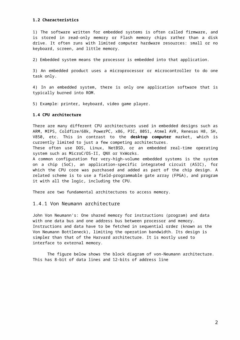
John Von Neumann's: One shared memory for instructions (program) and data with one data bus and one address bus between processor and memory. Instructions and data have to be fetched in sequential order (known as the Von Neumann Bottleneck), limiting the operation bandwidth. Its design is simpler than that of the Harvard architecture. It is mostly used to interface to external memory.
The figure below shows the block diagram of von-Neumann architecture. This has 8-bit of data lines and 12-bits of address line
1.4.2 Harvard architecture
The term originated from the Harvard Mark 1 relay-based computer, which stored instructions on punched tape and data in relay latches.
2

Harvard Architecture: The Harvard architecture uses physically separate memories for their instructions and data, requiring dedicated buses for each of them. Instructions and operands can therefore be fetched simultaneously.
Different program and data bus widths are possible, allowing program and data memory to be better optimized to the architectural requirements. E.g.: If the instruction format requires 14 bits then program bus and memory can be made 14-bit wide, while the data bus and data memory remain 8-bit wide.
1.4.3 Modified / Supper Harvard architecture
The Modified Harvard Architecture is a variation of the Harvard computer architecture that allows the contents of the instruction memory to be accessed as if it were data. Most modern computers that are documented as Harvard Architecture are, in fact, Modified Harvard Architecture. A pure Harvard architecture computer suffers from the disadvantage that mechanisms must be provided to separately load the program to be executed into instruction memory and any data to be operated upon into data memory. Additionally, modern Harvard architecture machines often use a read-only technology for the instruction memory and read/write technology for the data memory. This allows the computer to begin execution of a pre-loaded program as soon as power is applied.
The data memory will at this time be in an unknown state, so it is not possible to provide any kind of pre-defined data values to the program. The solution is to provide a hardware pathway and machine language instructions so that the contents of the instruction memory can be read as if they were data. Initial data values can then be copied from the instruction memory into the data memory when the program starts. If the data is not to be modified (for example, if it is a constant value, such as pi, or a text string), it can be accessed by the running program directly from instruction memory without taking up space in data memory (which is often at a premium).
1.4.4 Harvard or Von Neumann?
Three characteristics of Harvard architecture machines may be used to distinguish them from Von Neumann machines:
Instruction and data memories occupy different address spaces. That is, there is an address 'zero' in instruction space that refers to an instruction storage location and also an address 'zero' in data space that refers to a distinct data storage location. By contrast, a Von Neumann machine stores both instructions and data in a single address space, so address 'zero' refers to only one thing and whether the binary pattern in that location is interpreted as an instruction or data is defined by how the program is written. This characteristic unambiguously identifies a Harvard machine; that is, if instruction and data memories occupy different address spaces then the architecture is Harvard, not Von Neumann.
Instruction and data memories have separate hardware pathways to the central processing unit (CPU). This is pretty much the whole point of modern Harvard machines and why they still co-exist with the more flexible and general Von Neumann architecture. Separate memory pathways to the CPU allow instructions to be fetched and data to be accessed at the same time without the considerable extra complexity of a cache. Therefore, when performance is important but a cache in impractical (due to complexity or the difficulty of predicting execution speed) and the extra difficulty of programming a Harvard machine is acceptable, this becomes the architecture of choice. However, a Von Neumann machine with independent instruction and data caches also has separate hardware pathways to the CPU (for precisely the same purpose of increasing speed). Some processors are referred to as Harvard architecture even though instructions and data occupy the same address space because they cache instructions and data separately and pass them to the CPU via separate hardware pathways. As a result, this characteristic is no longer unambiguous. From a programmer's point-of-view, a processor with a single address space for instruction and data is programmed in the same way whether or not it has cache and is therefore a Von Neumann machine. From the point-of-view of the CPU designer, simultaneous access to instructions and data may appear sufficiently important to warrant a special term to distinguish the results from a Von Neumann machine with no cache or a unified cache.
Instruction and data memories are implemented in different ways. The original Harvard machine, the Mark I, stored instructions on a punched paper tape and data in electro-mechanical relays. This, however, was entirely due to the limitations of technology available at the time. Modern embedded computer systems (for example, the microcontroller in a digital camera) have the need to store their software programs without power and without the disk drives used in general purpose computers. Therefore, instructions are stored in a read-only memory technology. Read/write memory (which loses its contents when power is removed) is only used for data storage. There is no obstacle to combining
3
different memory technologies in a single address space and thus building a Von Neumann machine with read-only instructions and read/write data. So, this characteristic of the original Harvard machine is no longer relevant as a distinction from Von Neumann machines.
1.5. RISC vs. CISC
The simplest way to examine the advantages and disadvantages of RISC architecture is by contrasting it with it's predecessor: CISC (Complex Instruction Set Computers) architecture.
Multiplying Two Numbers in Memory
On the right is a diagram representing the storage scheme for a generic computer. The main memory is divided into locations numbered from (row) 1: (column) 1 to (row) 6: (column) 4. The execution unit is responsible for carrying out all computations. However, the execution unit can only operate on data that has been loaded into one of the six registers (A, B, C, D, E, or F). Let's say we want to find the product of two numbers - one stored in location 2:3 and another stored in location 5:2 - and then store the product back in the location 2:3.
1.5.1 The CISC Approach The primary goal of CISC architecture is to complete a task in as few lines of assembly as possible. This is achieved by building processor hardware that is capable of understanding and executing a series of operations. For this particular task, a CISC processor would come prepared with a specific instruction (we'll call it "MULT"). When executed, this instruction loads the two values into separate registers, multiplies the operands in the execution unit, and then stores the product in the appropriate register. Thus, the entire task of multiplying two numbers can be completed with one instruction:
MULT 2:3, 5:2
MULT is what is known as a "complex instruction." It operates directly on the computer's memory banks and does not require the programmer to explicitly call any loading or storing functions. It closely resembles a command in a higher level language. For instance, if we let "a" represent the value of 2:3 and "b" represent the value of 5:2, then this command is identical to the C statement "a = a * b."
One of the primary advantages of this system is that the compiler has to do very little work to translate a high-level language statement into assembly. Because the length of the code is relatively short, very little RAM is required to store instructions. The emphasis is put on building complex instructions directly into the hardware.
1.5.2 The RISC Approach RISC processors only use a small number of simple instruction and a few addressing mode that can be executed within one clock cycle. Thus, the "MULT" command described above could be divided into three separate commands: "LOAD," which moves data from the memory bank to a register, "PROD," which finds the product of two operands located within the registers, and "STORE," which moves data from a register to the memory banks. In order to perform the exact series of steps described in the CISC approach, a programmer would need to code four lines of assembly:
LOAD A, 2:3LOAD B, 5:2PROD A, BSTORE 2:3, A
At first, this may seem like a much less efficient way of completing the operation. Because there are more lines of code, more RAM is needed to store the assembly level instructions. The compiler must also perform more work to convert a high-level language statement into code of this form.
4

However, the RISC strategy also brings some very important advantages because each instruction requires only one clock cycle to execute, the entire program will execute in approximately the same amount of time as the multi-cycle "MULT" command. These RISC "reduced instructions" require less transistors of hardware space than the complex instructions, leaving more room for general purpose registers. Because all of the instructions execute in a uniform amount of time (i.e. one clock), pipelining is possible.
1.5.4 The Performance EquationThe following equation is commonly used for expressing a computer's performance ability:
The CISC approach attempts to minimize the number of instructions per program, sacrificing the number of cycles per instruction. RISC does the opposite, reducing the cycles per instruction at the cost of the number of instructions per program.
1.6 What is Microcontroller?
A microcontroller is an integrated chip that is often part of an embedded system. The microcontroller includes a CPU, RAM, ROM, I/O ports, and timers like a standard computer, but because they are designed to execute only a single specific task to control a single system, they are much smaller and simplified so that they can include all the functions required on a single chip.
Characteristics that define microcontrollers.
Microcontrollers are "embedded" inside some other device (often a consumer product) so that they can control the features or actions of the product. Another name for a microcontroller, therefore, is "embedded controller."
Microcontrollers are dedicated to one task and run one specific program. The program is stored in ROM (read-only memory) and generally does not change.
Microcontrollers are often low-power devices. A desktop computer is almost always plugged into a wall socket and might consume 50 watts of electricity. A battery-operated microcontroller might consume 50 milliwatts.
A microcontroller has a dedicated input device and often (but not always) has a small LED or LCD display for output. A microcontroller also takes input from the device it is controlling and controls the device by sending signals to different components in the device.
A microcontroller is often small and low cost. The components are chosen to minimize size and to be as inexpensive as possible.
1.6 Why do we need to learn Microprocessors/controllers?
1. The microprocessor is the core of computer system.2. Nowadays many communication, digital entertainment, portable device, are controlled by then.
3. A designer should know what types of components he need, ways to reduce production cost and product reliable.
1.6.1 Different aspects of a microprocessors/ controllers
Hardware: Interface to the real world
CISC RISC Emphasis on hardware Emphasis on software Includes multi-clockcomplex instructions
Single-clock,reduced instruction only
Memory-to-memory:"LOAD" and "STORE"incorporated in instructions
Register to register:"LOAD" and "STORE"are independent instructions
Small code sizes,high cycles per second
Low cycles per second,large code sizes
Transistors used for storingcomplex instructions
Spends more transistorson memory registers
5

Software : order how to deal with inputs
1.6.2 The necessary tools for a microprocessor/controller
CPU: Central Processing Unit I/O: Input /Output
Bus: Address bus & Data bus
Memory: RAM & ROM
Timer
Interrupt
Serial Port
Parallel Port
1.7 Microprocessors:
General-purpose microprocessor
CPU for Computers No RAM, ROM, I/O on CPU chip itself
Example:Intel’s x86, Motorola’s 680x0
1.8 Microcontroller:
A smaller computer On-chip RAM, ROM, I/O ports...
Example:Motorola’s 6811, Intel’s 8051, Zilog’s Z8 and PIC 16X
6

1.9 Microprocessor vs. Microcontroller
2.0 Three criteria in Choosing a Microcontroller
1. meeting the computing needs of the task efficiently and cost effectively• speed, the amount of ROM and RAM, the number of I/O ports and timers, size, packaging,
power consumption
• easy to upgrade
• cost per unit
2. availability of software development tools
• assemblers, debuggers, C compilers, emulator, simulator, technical support
3. Wide availability and reliable sources of the microcontrollers.
Chapter 2
8051 Microcontroller
2.0 Introduction
The Intel 8051 is a Harvard architecture, single chip microcontroller (µC) which was developed by Intel in 1980 for use in embedded systems. It was popular in the 1980s and early 1990s, but today it has largely been superseded by a vast range of enhanced devices with 8051-compatible processor cores that are manufactured by more than 20 independent manufacturers including Atmel, Infineon Technologies, Maxim Integrated Products (via its Dallas Semiconductor subsidiary), NXP (formerly Philips Semiconductor), Winbond, ST Microelectronics, Silicon Laboratories (formerly Cygnal), Texas Instruments and Cypress Semiconductor. Intel's official designation for the 8051 family of µCs is MCS 51.
Microprocessor CPU is stand-alone, RAM, ROM, I/O, timer
are separatedesigner can decide on the amount of ROM,
RAM and I/O ports.expansiveversatility general-purpose
MicrocontrollerCPU, RAM, ROM, I/O and timer are all on a
single chipfix amount of on-chip ROM, RAM, I/O portsfor applications in which cost, power and space
are criticalsingle-purpose
7

Intel's original 8051 family was developed using NMOS technology, but later versions, identified by a letter "C" in their name, e.g. 80C51, used CMOS technology and were less power-hungry than their NMOS predecessors - this made them eminently more suitable for battery-powered devices.
2.1 8051 Microcontroller
The 8051 is the original member of the 8051 family. Intel refers to it as MCS-51. The table shows the main features of the 8051
It provides many functions (CPU, RAM, ROM, I/O, interrupt logic, timer, etc.) in a single package
Feature Quantity
ROM 4K bytes(“program memory”)
RAM 128 bytes(Data memory”)
Timer 2 (each 16 bit)
I/O pins 32
Serial port 1
Interrupt sources 6
8-bit data bus - It can access 8 bits of data in one operation (hence it is an 8-bit microcontroller)
16-bit address bus - It can access 216 memory locations - 64 kB each of RAM and ROM
Other member of the 8051 family
There are two other member in the 8051 family of microcontrollers. They are the 8052 and the 8031.
Feature 8051 8052 8031
ROM 4K bytes 8K bytes 0K bytes
RAM 128 bytes 256 bytes 128
Timer 2 3 2
I/O pins 32 32 32
Serial port 1 1 1
Interrupt sources 6 8 6
8

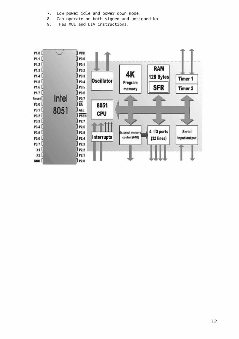
2.2 Internal block diagram
Now we are going to study about the architecture of 8051. It is shown in fig. On the basis of this architecture ATMEL developed the chip named as 80C51 and 89S51. The 89C51 is low power, high performance CMOS 8-bit microprocessor with 4 KB of flash programmable and erasable read only memory (PEROM). Flash memory allow the program memory to be reprogrammed in system or by non volatile memory program by combining the versatile 8 bit CPU with a monolithic chip, the ATMEL AT89C51 becomes a powerful micro computer, which provides a highly flexible and cost effective solution to many embedded control application. This is the reason it is used world wide.
As refer to the block diagram we can see that it has following things on the chips.1. On chip flash memory of 4 KB(Thousand Times Erasable and Reprogrammed)2. On chip RAM of 128 MB.3. Can be operated from 0 Hz to 24 MHz.4. 4 Input/Output ports of 8 lines each named as P0, P1, P2, and P3.5. Two Timer/Counter registers of 16 bit each (T0 and T1).
a) 3 External Interrupts…1) RESET 2) INT0 3) INT1
b) 3 Internal Interrupts… 1) IT0 2) IT1 3) S&R 6. Programmable serial Links by using the TxD and RxD lines. 7. Low power idle and power down mode. 8. Can operate on both signed and unsigned No. 9. Has MUL and DIV instructions.
9

8051 functional block diagram.
10

Fig Shows the external code memory and data memory connected to the 8051 chip.
Note – part of the external code memory can be located within the chip but we will ignore this feature for now. Also, variants of the chip will allow a lot more memory devices and I/O devices to be accommodate within the chip but such enhanced features will not be considered right now.
2.3 Pin diagram of Intel 8051
Pin Name Description Type
1 P1.0 or T2 Port 1 Bit 0 or Timer 2 External Input Input/Output
2 P1.1 or T2CAP Port 1 Bit 1 or Timer 2 External Reload/Capture Input/Output
3 P1.2 Port 1 Bit 2 Input/Output
4 P1.3 Port 1 Bit 3 Input/Output
5 P1.4 Port 1 Bit 4 Input/Output
6 P1.5 Port 1 Bit 5 Input/Output
7 P1.6 Port 1 Bit 6 Input/Output
11
8 P1.7 Port 1 Bit 7 Input/Output
9 Reset System Reset Input
10 P3.0 or RXD Port 3 Bit 0 or Serial Receive Input/Output
11 P3.1 or TXD Port 3 Bit 1 or Serial Transmit Input/Output
12 P3.2 or INT0 Port 3 Bit 2 or External Interrupt 0 Input/Output
13 P3.3 or INT1 Port 3 Bit 3 or External Interrupt 1 Input/Output
14 P3.4 or T0 Port 3 Bit 4 or Timer 0 External Input Input/Output
15 P3.5 or T1 Port 3 Bit 5 or Timer 1 External Input Input/Output
16 P3.6 or WR Port 3 Bit 6 or Write Strobe for External Memory Input/Output
17 P3.7 or RD Port 3 Bit 7 or Read Strobe for External Memory Input/Output
18 XTAL1 Crystal Input Input
19 XTAL2 Crystal Output Output
20 VSS Circuit Ground Input
21 P2.0 or Addr8 Port 2 Bit 0 or Address bit 8 Input/Output
22 P2.1 or Addr9 Port 2 Bit 1 or Address bit 9 Input/Output
23 P2.2 or Addr10 Port 2 Bit 2 or Address bit 10 Input/Output
24 P2.3 or Addr11 Port 2 Bit 3 or Address bit 11 Input/Output
25 P2.4 or Addr12 Port 2 Bit 4 or Address bit 12 Input/Output
26 P2.5 or Addr13 Port 2 Bit 5 or Address bit 13 Input/Output
27 P2.6 or Addr14 Port 2 Bit 6 or Address bit 14 Input/Output
28 P2.7 or Addr15 Port 2 Bit 7 or Address bit 15 Input/Output
29 PSEN Signal of this pin is used for reading from external program memory
(ROM).Output
30 ALE
This pin emits an impulse sequence with a frequency equal to 1/6 of the
frequency generated by the main oscillator. If external memory is used,
signal from this pin controls the additional register for temporary storage of
the lower address byte (A0 - A7). This pin also serves as a control input
during the writing of program to MCU.
Output
31 EA
When this pin is connected to the ground, MCU gets program instructions
from external program memory. In case that internal program memory is
used (common case), this pin should be connected to the positive supply
pole (VCC). During the loading of program to internal Flash memory, this
pin is at +12V
Input
32 P0.7 or Addr7/Data7 Port 0 Bit 7 or Address bit 7/Data bit 7 Input/Output
33 P0.6 or Addr6/Data6 Port 0 Bit 6 or Address bit 6/Data bit 6 Input/Output
12

34 P0.5 or Addr5/Data5 Port 0 Bit 5 or Address bit 5/Data bit 5 Input/Output
35 P0.4 or Addr4/Data4 Port 0 Bit 4 or Address bit 4/Data bit 4 Input/Output
36 P0.3 or Addr3/Data3 Port 0 Bit 3 or Address bit 3/Data bit 3 Input/Output
37 P0.2 or Addr2/Data2 Port 0 Bit 2 or Address bit 2/Data bit 2 Input/Output
38 P0.1 or Addr1/Data1 Port 0 Bit 1 or Address bit 1/Data bit 1 Input/Output
39 P0.0 or Addr0/Data0 Port 0 Bit 0 or Address bit 0/Data bit 0 Input/Output
40 VCC Supply Voltage Input
2.4 Simple comparison: Pentium vs. 8051
FEATURE 8051 PENTIUM COMMENTClock Speed 12Mhz. typical
but 60MHz. ICs available
1,000 MHz. (1GHz.) 8051 internally divides clock by 12 so for 12MHz. clock effective clock rate is just 1MHz.
Address bus 16 bits 32 bits 8051 can address 216, or 64Kbytes of memory.Pentium can address 232, or4 GigaBytes of memory.
Data bus 8 bits 64 bits Pentium’s wide bus allows very fast data transfers.
ALU width 8 bits 32 bits But - Pentium has multiple 32 bit ALUs – along with floating-point units.
Applications Domestic appliances, Peripherals, automotive etc.
Personal ComputersAnd other high performance areas.
Power consumption
Small fraction of a watt Tens of watts Pentium runs hot as power consumption increases with frequency.
Cost of chip About 2 Euros. In volume
About 200 Euros –Depending on spec.
2.5 MEMORY AND REGISTER ORGANISATION
The 8051 has a separate memory space for code (programs) and data. We will refer here to on-chip memory and external memory as shown in figure 1.5. In an actual implementation the external memory may, in fact, be contained within the microcomputer chip. However, we will use the definitions of internal and external memory to be consistent with 8051 instructions which operate on memory. Note, the separation of the code and data memory in the 8051 architecture is a little unusual. The separated memory architecture is referred to as Harvard architecture whereas Von Neumann architecture defines a system where code and data can share common memory.
13

8051Memoryrepresentation
2.6.1 External Code MemoryThe executable program code is stored in this code memory. The code memory size is limited to 64KBytes (in a standard 8051). The code memory is read-only in normal operation and is programmed under special conditions e.g. it is a PROM or a Flash RAM type of memory.
2.6.2 External RAM Data MemoryThis is read-write memory and is available for storage of data. Up to 64KBytes ofexternal RAM data memory is supported (in a standard 8051).
Internal Memory
The 8051’s on-chip memory consists of 256 memory bytes organised as follows:
First 128 bytes: 00h to 1Fh Register Banks20h to 2Fh Bit Addressable RAM30h to 7Fh General Purpose RAM
Next 128 bytes: 80h to FFh Special Function Register
The first 128 bytes of internal memory is organised as shown in figure, and is referred to as Internal RAM, or IRAM.
14
Programming Tip: Since code memory is restricted to 64K, 8051 programs are limited to 64K. Some assemblers and compilers offer ways to get around this limit when used with specially wired hardware. However, without such special compilers and hardware, programs are limited to 64K.
Programming Tip: The 8051 may only address 64k of RAM. To expand RAM beyond this limit requires programming and hardware tricks. You may have to do this "by hand" since many compilers and assemblers, while providing support for programs in excess of 64k, do not support more than 64k of RAM. This is rather strange since it has been my experience that programs can usually fit in 64k but often RAM is what is lacking. Thus if you need more than 64k of RAM, check to see if your compiler supports it-- but if it doesn't, be prepared to do it by hand.

As is illustrated in this map, the 8051 has a bank of 128 bytes of Internal RAM. This Internal RAM is found on-chip on the 8051 so it is the fastest RAM available, and it is also the most flexible in terms of reading, writing, and modifying its contents. Internal RAM is volatile, so when the 8051 is reset this memory is cleared. The 128 bytes of internal ram is subdivided as shown on the memory map. The first 8 bytes (00h - 07h) are "register bank 0". By manipulating certain SFRs, a program may choose to use register banks 0,1, 2, or 3. These alternative register banks are located in internal RAM in addresses 08h through 1Fh. We'll discuss "register banks" more in a later chapter. For now it is sufficient to know that they "live" and are part of internal RAM. Bit Memory also lives and is part of internal RAM. We'll talk more about bit memory very shortly, but for now just keep in mind that bit memory actually resides in internal RAM, from addresses 20h through 2Fh. The 80 bytes remaining of Internal RAM, from addresses 30h through 7Fh, may be used by user variables that need to be accessed frequently or at high-speed. This area is also utilized by the microcontroller as a storage area for the operating stack. This fact severely limits the 8051s stack since, as illustrated in the memory map, the area reserved for the stack is only 80 bytes--and usually it is less since this 80 bytes has to be shared between the stack and user variables.
2.7 Register BanksThe 8051 uses 8 "R" registers which are used in many of its instructions. These "R" registers are numbered from 0 through 7 (R0, R1, R2, R3, R4, R5, R6, and R7). These registers are generally used to assist in manipulating values and moving data from one memory location to another. For example, to add the value of R4 to the Accumulator, we would execute the following instruction:
2.8 Bit-addressable RAM The 8051, being a communications-oriented microcontroller, gives the user the ability to access a number of bit variables. These variables may be either 1 or 0. Of the 128-byte internal RAM of the 8051, only 16 bytes are bit-addressable. These 16 bytes provide 128 bits of RAM bit addressability since 16*8 = 128. They are addressed as 0 to 127(in decimal) or 00 to 7FH.
15
Programming Tip: If you only use the first register bank (i.e. bank 0), you may use Internal RAM locations 08h through 1Fh for your own use. But if you plan to use register banks 1, 2, or 3, be very careful about using addresses below 20h as you may end up overwriting the value of your "R" registers!

Instruction Function
SETB bit Set the bit(bit = 1)
CLR bit Clear the bit (bit = 0)
CPL bit Complement the bit(bit = NOT bit)
JB bit, target Jump to target if bit = 1(jump if bit)
JNB bit, target Jump to target if bit = 0(jump if no bit)
JBC bit, target Jump to target if bit = 1,clear bit(jump if bit,then clear)
EXAMPLE
SETB 24hIt is important to note that Bit Memory is really a part of Internal RAM. In fact, the 128 bit variables occupy the 16 bytes of Internal RAM from 20h through 2Fh. Thus, if you write the value FFh to Internal RAM address 20h you have effectively set bits 00h through 07h. That is to say that:
MOV 20h,#0FFh is equivalent to: SETB 00hSETB 01hSETB 02hSETB 03hSETB 04hSETB 05hSETB 06hSETB 07h
As illustrated above, bit memory isn’t really a new type of memory. Its really just a subset of Internal RAM. But since the 8051 provides special instructions to access these 16 bytes of memory on a bit by bit basis it is useful to think of it as a separate type of memory. However, always keep in mind that it is just a subset of Internal RAM--and that operations performed on Internal RAM can change the values of the bit variables. Bit variables 00h through 7Fh are for user-defined functions in their programs. However, bit variables 80h and above are actually used to access certain SFRs on a bit-by-bit basis. For example, if output lines P0.0 through P0.7 are all clear (0) and you want to turn on the P0.0 output line you may either execute:
MOV P0, # 01h Or you may execute: SETB 80h
Both these instructions accomplish the same thing. However, using the SETB command will turn on the P0.0 line without affecting the status of any of the other P0 output lines. The MOV command effectively turns off all the other output lines which, in some cases, may not be acceptable.
. 2.9 Special Function Register (SFR) Memory
Special Function Registers (SFRs) are areas of memory that control specific functionality of the 8051 processor. For example, four SFRs permit access to the 8051s 32 input/output lines. Another SFR allows a program to read or write to the 8051s serial port. Other SFRs allow the user to set the serial baud rate, control and access timers, and configure the 8051s interrupt system. When programming, SFRs have the illusion of being Internal Memory. For example, if you want to write the value "1" to Internal RAM location 50 hex you would execute the instruction:
16
Programming Tip: By default, the 8051 initializes the Stack Pointer (SP) to 07h when the microcontroller is booted. This means that the stack will start at address 08h and expand upwards. If you will be using the alternate register banks (banks 1, 2 or 3) you must initialize the stack pointer to an address above the highest register bank you will be using, otherwise the stack will overwrite your alternate register banks.
Programming Tip: If your program does not use bit variables, you may use Internal RAM locations 20h through 2Fh for your own use. But if you plan to use bit variables, be very careful about using addresses from 20h through 2Fh as you may end up overwriting the value of your bits!

MOV 50h, # 01hSimilarly, if you want to write the value "1" to the 8051s serial port you would write this value to the SBUF SFR, which has an SFR address of 99 Hex. Thus, to write the value "1" to the serial port you would execute the instruction:
MOV 99h, # 01hAs you can see, it appears that the SFR is part of Internal Memory. This is not the case. When using this method of memory access (its called direct address), any instruction that has an address of 00h through 7Fh refers to an Internal RAM memory address; any instruction with an address of 80h through FFh refers to an SFR control register.
2.10 What Are SFRs?
The 8051 is a flexible microcontroller with a relatively large number of modes of operations. Your program may inspect and/or change the operating mode of the 8051 by manipulating the values of the 8051's Special Function Registers (SFRs). SFRs are accessed as if they were normal Internal RAM. The only difference is that Internal RAM is from address 00h through 7Fh whereas SFR registers exist in the address range of 80h through FFh. Each SFR has an address (80h through FFh) and a name. The following chart provides a graphical presentation of the 8051's SFRs, their names, and their address.
As you can see, although the address range of 80h through FFh offer 128 possible addresses, there are only 21 SFRs in a standard 8051. All other addresses in the SFR range (80h through FFh) are considered invalid. Writing to or reading from these registers may produce undefined values or behavior.
2.11 SFR DescriptionsThis section will endeavour to quickly overview each of the standard SFRs found in the above SFR chart map. It is not the intention of this section to fully explain the functionality of each SFR--this information will be covered in separate chapters of the tutorial. This section is to just give you a general idea of what each SFR does.
P0 (Port 0, Address 80h, Bit-Addressable): This is input/output port 0. Each bit of this SFR corresponds to one of the pins on the microcontroller. For example, bit 0 of port 0 is pin P0.0, bit 7 is pin P0.7. Writing a value of 1 to a bit of this SFR will send a high level on the corresponding I/O pin whereas a value of 0 will bring it to a low level. If external memory is used, these pins are used for alternate transfer of data and addresses (A0-A7) 0for accessing the extra memory chip. Signal on ALE pin determines the mode of transfer on port.
17
Programming Tip: While the 8051 has four I/O port (P0, P1, P2, and P3), if your hardware uses external RAM or external code memory (i.e., your program is stored in an external ROM or EPROM chip or if you are using external RAM chips) you may not use P0 or P2. This is because the 8051 uses ports P0 and P2 to address the external memory. Thus if you are using external RAM or code memory you may only use ports P1 and P3 for your own use.

P1 (Port 1, Address 90h, Bit-Addressable): This is input/output port 1. Each bit of this SFR
corresponds to one of the pins on the microcontroller. For example, bit 0 of port 1 is pin P1.0, bit 7
is pin P1.7. Writing a value of 1 to a bit of this SFR will send a high level on the corresponding I/O
pin whereas a value of 0 will bring it to a low level. pins of Port 1 have alternate functions
according to the following table:
Pin Alternate function
P1.0 T2 (Timer 2 input)
P1.1 T2EX (Timer 2 control input)
P1.4 SS (SPI control input)
P1.5 MOSI (I/O of SPI system)
P1.6 MISO (I/O of SPI system)
P1.7 SCK (SPI clock signal)
P2 (Port 2, Address A0h, Bit-Addressable): This is input/output port 2. Each bit of this SFR corresponds to one of the pins on the microcontroller. For example, bit 0 of port 2 is pin P2.0, bit 7 is pin P2.7. Writing a value of 1 to a bit of this SFR will send a high level on the corresponding I/O pin whereas a value of 0 will bring it to a low level.
P3 (Port 3, Address B0h, Bit-Addressable): This is input/output port 3. Each bit of this SFR corresponds to one of the pins on the microcontroller. For example, bit 0 of port 3 is pin P3.0, bit 7 is pin P3.7. Writing a value of 1 to a bit of this SFR will send a high level on the corresponding I/O pin whereas a value of 0 will bring it to a low level.
Pin Alternate function
P3.0 RXD (Serial input)
18
Programming Tip: While the 8051 has four I/O port (P0, P1, P2, and P3), if your hardware uses external RAM or external code memory (i.e., your program is stored in an external ROM or EPROM chip or if you are using external RAM chips) you may not use P0 or P2. This is because the 8051 uses ports P0 and P2 to address the external memory. Thus if you are using external RAM or code memory you may only use ports P1 and P3 for your own use.

P3.1 TXD (Serial output)
P3.2 INT0 (External interrupt 0)
P3.3 INT1 (External interrupt 1)
P3.4 T0 (Timer 0 external input)
P3.5 T1 (Timer 1 external input)
P3.6 WR (Signal write to external
memory)
P3.7 RD (Signal read from external
memory)
SP (Stack Pointer, Address 81h): This is the stack pointer of the microcontroller. This SFR indicates where the next value to be taken from the stack will be read from in Internal RAM. If you push a value onto the stack, the value will be written to the address of SP + 1. That is to say, if SP holds the value 07h, a PUSH instruction will push the value onto the stack at address 08h. This SFR is modified by all instructions which modify the stack, such as PUSH, POP, LCALL, RET, RETI, and whenever interrupts are provoked by the microcontroller.
DPL/DPH (Data Pointer Low/High, Addresses 82h/83h): The SFRs DPL and DPH work together to represent a 16-bit value called the Data Pointer. The data pointer is used in operations regarding external RAM and some instructions involving code memory. Since it is an unsigned two-byte integer value, it can represent values from 0000h to FFFFh (0 through 65,535 decimal).
PCON (Power Control, Addresses 87h): The Power Control SFR is used to control the 8051's power control modes. Certain operation modes of the 8051 allow the 8051 to go into a type of "sleep" mode which requires much less power. These modes of operation are controlled through PCON. Additionally, one of the bits in PCON is used to double the effective baud rate of the 8051's serial port.
TCON (Timer Control, Addresses 88h, Bit-Addressable): The Timer Control SFR is used to configure and modify the way in which the 8051's two timers operate. This SFR controls whether each of the two timers is running or stopped and contains a flag to indicate that each timer has overflowed. Additionally, some non-timer related bits are located in the TCON SFR. These bits are used to configure the way in which the external interrupts are activated and also contain the external interrupt flags which are set when an external interrupt has occured.
TMOD (Timer Mode, Addresses 89h): The Timer Mode SFR is used to configure the mode of operation of each of the two timers. Using this SFR your program may configure each timer to be a 16-bit timer, an 8-bit autoreload timer, a 13-bit timer, or two separate timers. Additionally, you may
19
Programming Tip: The SP SFR, on startup, is initialized to 07h. This means the stack will start at 08h and start expanding upward in internal RAM. Since alternate register banks 1, 2, and 3 as well as the user bit variables occupy internal RAM from addresses 08h through 2Fh, it is necessary to initialize SP in your program to some other value if you will be using the alternate register banks and/or bit memory. It's not a bad idea to initialize SP to 2Fh as the first instruction of every one of your programs unless you are 100% sure you will not be using the register banks and bit variables.
Programming Tip: DPTR is really DPH and DPL taken together as a 16-bit value. In reality, you almost always have to deal with DPTR one byte at a time. For example, to push DPTR onto the stack you must first push DPL and then DPH. You can't simply plush DPTR onto the stack. Additionally, there is an instruction to "increment DPTR." When you execute this instruction, the two bytes are operated upon as a 16-bit value. However, there is no instruction that decrements DPTR. If you wish to decrement the value of DPTR, you must write your own code to do so.

configure the timers to only count when an external pin is activated or to count "events" that are indicated on an external pin.
TL0/TH0 (Timer 0 Low/High, Addresses 8Ah/8Ch): These two SFRs, taken together, represent timer 0. Their exact behavior depends on how the timer is configured in the TMOD SFR; however, these timers always count up. What is configurable is how and when they increment in value.
TL1/TH1 (Timer 1 Low/High, Addresses 8Bh/8Dh): These two SFRs, taken together, represent timer 1. Their exact behavior depends on how the timer is configured in the TMOD SFR; however, these timers always count up. What is configurable is how and when they increment in value.
SCON (Serial Control, Addresses 98h, Bit-Addressable): The Serial Control SFR is used to configure the behaviour of the 8051's on-board serial port. This SFR controls the baud rate of the serial port, whether the serial port is activated to receive data, and also contains flags that are set when a byte is successfully sent or received.
Bit Name Bit Address Purpose
SM0 9Fh Mode of work
SM1 9Eh Mode of work
SM2 9Dh Enables connecting multiple MCU's
REM 9Ch When set, enables receiving data
TB8 9Bh 9th bit for sending data in modes 2 and 3
RB8 9Ah 9th bit for sending data in modes 2 and 3
TI 99h Bit is automatically set when the whole byte is sent
RI 98h Bit is automatically set when the whole byte is
received
As shown in the table, combination of bits SM0 and SM1 determines the mode of work for serial port:
SM0 SM1 Mode Description Baud Rate
0 0 0 8-bit Shift register Quartz frequency / 12
0 1 1 8-bit UART Determined by timer T1 or T2
1 0 2 9-bit UART Quartz frequency / 32
1 1 3 9-bit UART Determined by timer T1 or T2
SBUF (Serial Control, Addresses 99h): The Serial Buffer SFR is used to send and receive data via the on-board serial port. Any value written to SBUF will be sent out the serial port's TXD pin. Likewise, any value which the 8051 receives via the serial port's RXD pin will be delivered to the user program via SBUF. In other words, SBUF serves as the output port when written to and as an input port when read from.
20
Programming Tip: To use the 8051's on-board serial port, it is generally necessary to initialize the following SFRs: SCON, TCON, and TMOD. This is because SCON controls the serial port. However, in most cases the program will wish to use one of the timers to establish the serial port's baud rate. In this case, it is necessary to configure timer 1 by initializing TCON and TMOD.
IE (Interrupt Enable, Addresses A8h): The Interrupt Enable SFR is used to enable and disable specific interrupts. The low 7 bits of the SFR are used to enable/disable the specific interrupts, where as the highest bit is used to enable or disable ALL interrupts. Thus, if the high bit of IE is 0 all interrupts are disabled regardless of whether an individual interrupt is enabled by setting a lower bit.
Following table describes the bits of register IE
(same rule applies to all bits - logical state of 1 enables the appropriate interrupt):
Bit Purpose
EA Enables/disables all interrupt sources
ET2 Timer T2 interrupt
ES UART and SPI interrupts
ET1 Timer T1 interrupt
EX1 External interrupt: pin INT1
ET0 Timer T0 interrupt
EX0 External interrupt: pin INT0
IP (Interrupt Priority, Addresses B8h, Bit-Addressable): The Interrupt Priority SFR is used to specify the relative priority of each interrupt. On the 8051, an interrupt may either be of low (0) priority or high (1) priority. An interrupt may only interrupt interrupts of lower priority. For example, if we configure the 8051 so that all interrupts are of low priority except the serial interrupt, the serial interrupt will always be able to interrupt the system, even if another interrupt is currently executing. However, if a serial interrupt is executing no other interrupt will be able to interrupt the serial interrupt routine since the serial interrupt routine has the highest priority.
SFR register IP determines the priority of existing interrupt sources
(Same rule applies to all bits : logical state of 1 assigns higher priority to the appropriate
interrupt):
Bit Purpose
PT2 Timer T2 interrupt priority
PS Serial port interrupt priority
PT1 Timer T1 interrupt priority
PX1 External interrupt INT1 priority
PT0 Timer T0 interrupt priority
PX0 External interrupt INT0 priority
If two interrupt requests collide, the one with higher priority has precedence in execution. If both interrupts are of
same priority, the one with the later request has to hold one and let the controller handle the first one.
21

PSW (Program Status Word, Addresses D0h, Bit-Addressable): The Program Status Word is used to store a number of important bits that are set and cleared by 8051 instructions. The PSW SFR contains the carry flag, the auxiliary carry flag, the overflow flag, and the parity flag. Additionally, the PSW register contains the register bank select flags which are used to select which of the "R" register banks are currently selected.
Symbol Bit Address DescriptionC (or CY) PSW.7 D7h Carry flagAC PSW.6 D6h Auxiliary carry flagF0 PSW.5 D5h Flag 0RS1 PSW.4 D4h Register bank select 1RS0 PSW.3 D3h Register bank select 00V PSW.2 D2h Overflow flag
PSW.1 D1h ReservedP PSW.0 D0h Even Parity flag
P (bit 0) - Parity bit. If numeral in accumulator is even, bit is automatically set (1), otherwise it's cleared
(0). It is commonly used in data transfers via serial connection.
- (bit 1) - This bit is intended for the upcoming MCU models and shouldn't be used.
OV (bit 2) - Overflow bit. If result of arithmetical operation exceeds 255 (decimal), OV is set (1),
otherwise it's cleared (0).
RS1, RS0 (bits 3 and 4) - Register select. Masking these bits stores registers R0 - R7 into
one of the 4 banks in RAM, according to the following table.
RS1 RS2 Location in RAM
0 0 Bank 0 00h-07h
0 1 Bank 1 08h-0Fh
1 0 Bank 2 10h-17h
1 1 Bank 3 18h-1Fh
F0 (bit 5) - Flag 0. An all-purpose flag.
AC (bit 6) - Auxiliary Carry Flag, used only for operations with BCD (Binary Coded Decimals).
CY (bit 7) - Carry Flag. Auxiliary (ninth) bit for arithmetical and shift operations.
ACC (Accumulator, Addresses E0h, Bit-Addressable): The Accumulator is one of the most-used SFRs on the 8051 since it is involved in so many instructions. The Accumulator resides as an SFR at E0h, which means the instruction MOV A,#20h is really the same as MOV E0h,#20h. However, it is a
22
Programming Tip: If you write an interrupt handler routine, it is a very good idea to always save the PSW SFR on the stack and restore it when your interrupt is complete. Many 8051 instructions modify the bits of PSW. If your interrupt routine does not guarantee that PSW is the same upon exit as it was upon entry, your program is bound to behave rather erratically and unpredictably--and it will be tricky to debug since the behaviour will tend not to make any sense.

good idea to use the first method since it only requires two bytes whereas the second option requires three bytes.
B (B Register, Addresses F0h, Bit-Addressable): The "B" register is used in two instructions: the multiply and divide operations. The B register is also commonly used by programmers as an auxiliary register to temporarily store values.
2.12 ADDRESSING MODES
An "addressing mode" refers to how you are addressing a given memory location. In summary, the addressing modes are as follows, with an example of each:
Immediate Addressing MOV A,#20h
Direct Addressing MOV A,30h
Indirect Addressing MOV A,@R0
External Direct MOVX A,@DPTR
Code Indirect MOVC A,@A+DPTR
Each of these addressing modes provides important flexibility. a. Immediate Addressing
Immediate addressing is so-named because the value to be stored in memory immediately follows the operation code in memory. That is to say, the instruction itself dictates what value will be stored in memory. For example, the instruction:
MOV A,#20h This instruction uses Immediate Addressing because the Accumulator will be loaded with the value that immediately follows; in this case 20 (hexidecimal). Immediate addressing is very fast since the value to be loaded is included in the instruction. However, since the value to be loaded is fixed at compile-time it is not very flexible.
b. Direct AddressingDirect addressing is so-named because the value to be stored in memory is obtained by directly retrieving it from another memory location. For example:
MOV A,30h This instruction will read the data out of Internal RAM address 30 (hexidecimal) and store it in the Accumulator. Direct addressing is generally fast since, although the value to be loaded isnt included in the instruction, it is quickly accessable since it is stored in the 8051s Internal RAM. It is also much more flexible than Immediate Addressing since the value to be loaded is whatever is found at the given address--which may be variable. Indirect Addressing
Indirect addressing is a very powerful addressing mode which in many cases provides an exceptional level of flexibility. Indirect addressing is also the only way to access the extra 128 bytes of Internal RAM found on an 8052. Indirect addressing appears as follows:
MOV A,@R0 This instruction causes the 8051 to analyze the value of the R0 register. The 8051 will then load the accumulator with the value from Internal RAM which is found at the address indicated by R0. For example, lets say R0 holds the value 40h and Internal RAM address 40h holds the value 67h. When the above instruction is executed the 8051 will check the value of R0. Since R0 holds 40h the 8051 will get the value out of Internal RAM address 40h (which holds 67h) and store it in the Accumulator. Thus, the Accumulator ends up holding 67h. Indirect addressing always refers to Internal RAM; it never refers to an SFR. Thus, in a prior example we mentioned that SFR 99h can be used to write a value to the serial port. Thus one may think that the following would be a valid solution to write the value 1 to the serial port:
MOV R0,#99h ;Load the address of the serial portMOV @R0,#01h ;Send 01 to the serial port -- WRONG!!
23

C.External DirectExternal Memory is accessed using a suite of instructions which use what I call "External Direct"
addressing. I call it this because it appears to be direct addressing, but it is used to access external memory rather than internal memory. There are only two commands that use External Direct addressing mode:
MOVX A,@DPTRMOVX @DPTR,A
As you can see, both commands utilize DPTR. In these instructions, DPTR must first be loaded with the address of external memory that you wish to read or write. Once DPTR holds the correct external memory address, the first command will move the contents of that external memory address into the Accumulator. The second command will do the opposite: it will allow you to write the value of the Accumulator to the external memory address pointed to by DPTR.
c. External IndirectExternal memory can also be accessed using a form of indirect addressing which I call External
Indirect addressing. This form of addressing is usually only used in relatively small projects that have a very small amount of external RAM. An example of this addressing mode is:
MOVX @R0,A Once again, the value of R0 is first read and the value of the Accumulator is written to that address in External RAM. Since the value of @R0 can only be 00h through FFh the project would effectively be limited to 256 bytes of External RAM. There are relatively simple hardware/software tricks that can be implemented to access more than 256 bytes of memory using External Indirect addressing; however, it is usually easier to use External Direct addressing if your project has more than 256 bytes of External RAM.
CHAPTER-3
3.1 Instruction Set
The 8051 family's instruction set consists of single byte OP-CODE followed by 0/1/2 bytes with immediate data or an 8 or 16 bit address. Instructions take 12 clock cycles (60% of them) or 24 clock cycles.
While only having 33 instructions the variety of different addressing modes means that depending on which variant of the move instruction is used MOV? R1,XXX then the XXX can refer to; a location in the 256 Internal Memory, to the I/O ports or to the bottom 256 bytes of External RAM. In some instructions the contents of certain Registers may act as 8 bit pointers to 256 of the external or internal memory bytes. There are significant restrictions on which addressing modes each instruction type can use (in the jargon it does not have a symmetrical instruction set), so its difficult to summarise the instruction set in a few words, it takes 40 page to specify it. This then is a personal brief summary trying to highlight its strengths and weaknesses.
3.2 Control instructions
Jumps and Calls with 16 bit addresses allow control to pass to any part of the 64K code space. 11 bit Jumps and Calls provide compatibility with the 8048 and efficient movement within a 2K module. Fast conditional Jumps are possible +/- 128 bytes of the current address and a Jump is provide that adds the AC to the contents of the DPTR to provide vectored jump tables.
Good things about the instruction set........
a. Most of the above operations use 1 or 2 bytes for an instruction so are fast and compactb. Manipulation of bits and bytes is easy
c. I/O and the on-chip 128 or 256 of RAM are easily and quickly read and written
d. So writing in assembler can create very compact code that handles I/O well
Bad things about this.......
24

a. It’s not a very clean assembler to come to terms with if you are new to writing assembler codeb. The need to do all arithmetic via the Accumulator can be a significant bottleneck
c. Careful control and usage of the Registers is necessary
3.3 Number Representation for Different Bases
The following is an example showing the decimal number 46 represented in different number bases:
46d ; 46 decimal2Eh ; 2Eh is 46 decimal represented as a hex number56o ; 56o is 46 decimal represented as an octal number101110b; 101110b is 46 decimal represented as a binary number.
Note a number digit must be used in the first character of a hexadecimal number. For example the hexadecimal number A5h is illegally represented and should be represented as 0A5h.
3.4 The Arithmetic OperatorsThe arithmetic operators are:
+ add- subtract* multiply/ divideMOD modulo (result is the remainder following division)
The Logical OperatorsThe logical operators are:
AND Logical ANDOR Logical ORXOR Logical XOR (exclusive OR)NOT Logical NOT
3.5 The Relational OperatorsThe result of a relational operation is either true (represented by minus 1), or false (represented by zero). The relational operators are:
Equal to EQ =not equal to NE <>greater than GT >greater than or equal to GE >=less than LT <less than or equal to LE <=
(note ‘EQ’ symbol and ‘= ‘ symbol have the same meaning)
3.6 Operator PrecedenceLike a high level language, assembly level programs define operator predence. Operators with same precedence are evaluated left to right. Note, brackets ( ) means to evaluate this first. HIGH indicates the high-byte and LOW indicates the low-byte. Later examples will clarify the use of such special operators. The precedence list, highest first, is as follows:
( )HIGH LOW* / MOD SHL SHR+ -= <> < <= > >=NOTANDOR XOR
25

3.7 Some Assembler DirectivesThe assembler directives are special instruction to the assembler program to define some specific operations but these directives are not part of the executable program. Some of the most frequently assembler directives are listed as follows:
ORG Originate, defines the starting address for the program in program(Code) memory
EQU Equate, assigns a numeric value to a symbol identifier so as to makeThe program more readable. The following uses EQU for the counter constant and then the constant is used to load the R3 register.
WRITE EQU 65…… …….MOV R2, # WRITE When executing the instruction “MOV R3, # WRITE”, the register R3 will be loaded with the value 25By the use of EQU , the programmer can change it once and the assembler will change all it’s occurrence.
DB Define a Byte, puts a byte (8-bit number) number constant at thismemory location. The DB directive is the only directive that can be used to define ASCII strings larger than two character ; therefore, it should be used for all ASCII data definitionFor ExampleORG 600HDATA1: DB “Hello how are you”
DW Define a Word, puts a word (16-bit number) number constant at thismemory location
DBIT Define a Bit, defines a bit constant, which is stored in the bitaddressable section if the Internal RAM.
END This is the last statement in the source file to advise the assembler tostop the assembly process.
26

27

28

29

CHAPTER-4
4.1 ASSEMBLER INTRODUCTION
4.2 What is an Assembler?
An assembler is a program that translates symbolic code (assembly language) into executable object code. This object code can be executed with a 80C51-compatible microcontroller. If you have ever written a computer program directly in machine-recognizable form, such as binary or hexadecimal code, you will appreciate the advantages of programming in symbolic assembly language.
Assembly language operation codes (mnemonics) are easily remembered (MOV for move instructions, ADD for addition, and so on). You can also symbolically express addresses and values referenced in the operand field of instructions. Because you assign these names, you can make them as meaningful as the mnemonics for the instructions. For example, if your program must manipulate a date as data, you can assign it the symbolic name DATE. If your program contains a set of instructions used as a timing loop (executed repeatedly until a specific amount of time has passed), you can name the instruction group TIMER_LOOP.
An assembly program has three parts:
Machine instructions - Code the machine can execute. Detailed discussion of the machine instructions is in the hardware manuals of the 80C51 microcontroller.
Assembler directives - Define the program structure and symbols, and generate non executable code (data, messages, and so on.).
Assembler controls - Set assembly modes and direct assembly flow.
Output Files
The Ax51 Assembler generates a number of output files during compilation. By default, each output file shares the same filename as the source file. However, each has a different file extension. The following table lists the files and gives a brief description of each.
File Extension Description
.LST Files with this extension are listing files that contain the formatted source text along with any errors detected by the assembler. Listing files may optionally contain the symbols used and a cross reference. Refer to the PRINT directive for more information.
.OBJ Files with this extension are object modules that contain relocatable object code. Object modules may be linked to an absolute object module by the Lx51 or BL51 Linkers.
4.3 Creating a Project
The required steps for creating a project and application programs are:
30

1. μVision2 is a standard Windows application and started by clicking on the program icon. To create a new project file select from the μVision2 menu Project – New Project…. This opens a standard Windows dialog that asks youfor the new project file name.
2. We suggest that you use a separate folder for each project. You can simply use the icon Create New Folder in this dialog to get a new empty folder. For example here your folder name is abc
31

3. Then select this folder and enter the file name for the new project, i.e. Project1.μVision2 creates a new project file with the name PROJECT1.Z which contains a default target and file group name. You can see these names in the Project Window – Files.for example the file name for your new project is cde.
4. Now use from the menu Project – Select Device for Target and select a CPUFor your project. The Select Device dialog box shows the μVision2 device Database. Just select the microcontroller you use. For example here we choose 8052
32

4. You may create a new source file with the menu option File – New. This opens an empty editor window where you can enter your source code.
33

5. μVision2enables the C color syntax highlighting when you save your file with the dialogFile – Save As… under a filename with the extension *.C. We are saving ourexample file under the name MAIN.C.
34

For example saved your file efg.c use .c extension for the ‘C’ source file and .asm for assembly source file
Clicks save
μVision2 offers several ways to add source files to a project. For example, youcan select the file group in the Project Window – Files page and click with theright mouse key to open a local menu. The option Add Files opens the standardfiles dialog. Select the file MAIN.C you have just created.
35

For example here you have add your file efg
36

Make your own program
37

Compile your program
Once you have successfully generated your application you can start debugging.After you have tested your application, it isrequired to create an Intel HEX file to download the software into an EPROM programmer or simulator. μVision2 creates HEX files with each build process when Create HEX file under Options for Target – Output is enabled.
38

Again compile your program.
39

4.6 Introduction of ‘c’
C can be a rather terse and mystifying language. Widely quoted as being a high level language, C does indeed contain many such features like structured programming, defined procedure calling, parameter passing, powerful control structures etc.However much of the power of C lies in its ability to combine simple, low-level commands into complicated high-level language-like functions and allow access to the actual bytes and words of the host processor. To a great extent then, C is a sort of universal assembly language. Most programmers who are familiar with C will have been used to writing programs within large machines running UNIX or latterly MS-DOS. Even in the now cramped 640KB of MS-DOS, considerable space is available so that the smallest variable in a program will be an int (16-bits). Most interfacing to the real world will be done via DOS Mints and function calls. Thus the actual C written is concerned only with the manipulation and processing of variables, strings, arrays etc. Within the modern 8 bit microcontroller, however, the situation is somewhat different. Taking the 8051 as an example, the total program size can only occupy 4 or 8K and use only 128bytes of RAM. Ideally, real devices such as ports and special function registers must be addressed from C. Interrupts have to be serviced, which require vectors at absolute addresses. Special care must be taken with a routine’s data memory allocation if over-writing of background loop data is to be avoided. One of the fundamentals of C is that parameters (input variables) are passed to a function (subroutine) and results returned to the caller via the stack. Thus a function can be called from both interrupts and the background without fear of its local data being overwritten (re-currency). A serious restriction with the 8051 family is the lack of a proper stack; typically with a processor such as the 8086, the stack pointer is 16-bits (at least). Besides the basic stack pointer, there are usually other stack relative pointers such as a base pointer etc. 4.7 WHY USE C?
It is a ‘mid level’, with high level features(such as support for functions and modules), and low level features(such as good access to hardware via pointers);
It is very efficient; It is popular and well understood; Good, well-proven compilers are available for every embedded processor(8-bit to 32-bit or more); Experienced staff are available;
The “super loop” software architecture
Problem What is the minimum software environment you need to create an embedded C program ?
Solution
void main (void){ X_Init (); While (1) /* for ever (super loop) */
{ X (); /* perform the task */
}}
40

Crucially the ‘super loop’ or ‘endless loop’ is required because we have no operating system to return to: our application will keep looking until the system power is removed.
4.8 Strengths and weakness of ‘super loops’.
The main strength of super loop is there simplicity. This makes them (comparatively) easy to build, test and maintain.
It is highly portable.
But If your application requires accurate timing, then this frame work will not provide the accuracy or
flexibility you require.
4.9 Data Types
The Cx51 Compiler provides several basic data types you may use in your C programs. The compiler supports the standard C data types as well as several data types that are unique to the Cx51 platform.
Data Types Bits Bytes Value Rangebit 1 0 to 1signed char 8 1 -128 to +127unsigned char 8 1 0 to 255enum 8 / 161 or 2-128 to +127 or -32768 to +32767signed short 16 2 -32768 to +32767unsigned short16 2 0 to 65535signed int 16 2 -32768 to +32767unsigned int 16 2 0 to 65535signed long 32 4 -2147483648 to +2147483647unsigned long 32 4 0 to 4294967295float 32 4 ±1.175494E-38 to ±3.402823E+38sbit 1 0 or 1sfr 8 1 0 to 255sfr16 16 2 0 to 65535
Note: The bit, sbit, sfr, and sfr16 data types are not provided in ANSI C. They are unique to the Cx51 Compiler.
4.10 Bitwise OperatorsC provides six operators for bit manipulation; these may only be applied to integral operands,that is, char, short, int, and long, whether signed or unsigned.
& bitwise AND| bitwise inclusive OR^ bitwise exclusive OR<< left shift>> right shift~ one's complement (unary)
4.11 Function Declarations
The C51 Compiler provides a number of extensions for standard C function declarations. These extensions allow you to:
Declare a function as an interrupt procedure Choose the register bank used Select the memory model Declare a reentrant function Declare alien (PL/M-51) functions
41

You may include these extensions or attributes (many of which may be combined) in the function declaration. Use the following standard format for your C51 Compiler function declarations.
« return_type » funcname (« args ») « {small | compact | large} » « reentrant » « interrupt x » « using y »
Where
return_type Is the type of the value returned from the function. If no type is specified, int is assumed.funcname is the name of the function.args is the argument list for the function.small explicitly defines the function uses the small memory model.compact explicitly defines the function uses the compact memory model.large explicitly defines the function uses the large memory model.reentrant indicates that the function is recursive or re-entrant.interrupt indicates that the function is an interrupt function.x is the interrupt number.using specifies which register bank the function uses.y is the register bank number.
Descriptions of these attributes and other features are described in detail in the following sections.
4.12 Preprocessor
The preprocessor built into the Cx51 Compiler processes the source text of a source file before it is actually compiled into machine language and object code. Preprocessing is the first thing the compiler does. The purpose of the preprocessor is to replace or insert additional text into the source file just prior to compilation.
Most of the obvious functions of the preprocessor require activation (by including preprocessor directives) in your source code. However, there are several things the preprocessor always does:
Each C comment is replaced by a single space.
Line continuations (indicated by a backslash ('\') at the end of a line) are removed and the lines they break apart are joined for compilation.
Predefined macro names are replaced with their predefined text.
In addition to these operations, the pre-processor in the Cx51 Compiler supports the more obvious pre-processor operations:
Header Files,
Macros, Conditional Compilation.
If you encounter pre-processor problems, you may direct the compiler to generate a Pre-processor File that shows the exact output from the pre-processor.
4.13 Header Files
Header files or include files are included and processed by the pre-processor. They provide you with a convenient way to publish global variables, function prototypes, manifest constants, and macro definitions that are used throughout a large development effort.
The #include directive specifies the name of the header file to include.
42

4.14 Macros
Perhaps the most useful aspect of the C pre-processor is the ability to create and use macros. Macros enable you to assign short names to source code blocks. When you use the macro name in your source file, the pre-processor replaces it with the source code block specified in the macro definition.
A macro definition includes the name of the macro, the macro body, and may include macro arguments.
Simple Macros require no arguments and are the simplest macros to define.
Complex Macros accept one or more arguments and may be used like functions. Macro Operators lists special macro operators that may be used in macro definitions. Predefined Macros lists macros that are defined by the compiler at compile-time.
4.15 Simple Macros
A simple macro is merely an abbreviation for a fragment of code. It is often called a manifest constant because it defines a name for a constant value.
Macros must be defined using the #define directive before they can be used. For example:
#define LEN 128
defines a macro named LEN. When LEN is used in your program (or in preprocessor directives) it is replaced with the text 128. So, a C statement like
char buffer[LEN];
is expanded by the preprocessor into
char buffer[128];
and is subsequently compiled by the compiler.
Note: Macro definitions must be a single line. You may use the backslash character ('\') followed by a new-line to continue a macro on a subsequent line (refer to Preprocessor Directives for more information).
By convention, macro names are uppercase. If you maintain that convention in your applications, it is easy to tell at a glance if an object is a variable, a function, or a macro.
4.16 Complex Macros
A complex macro accepts arguments and generates a fragment of code using the values of those arguments. Macros that accept arguments appear to be functions. However, arguments are not typed as in a C function. They are merely replaced by the text passed to the macro when expanded.
Macros with arguments must be defined using the #define directive before they can be used. The argument list is enclosed in parentheses and must immediately follow the macro name. Spaces are not allowed between and macro name and open parenthesis. For example:
#define MAX(x,y) ((x) > (y) ? (x) : (y))
defines a macro named MAX that takes two arguments (x and y). When MAX is used in your program (or in preprocessor directives) it is replaced with the text ((x) > (y) ? (x) : (y)). If x and y are numeric constants, the preprocessor can determine the result of the macro and substitute the greater value.
A C statement like
int a = MAX(15,20);
is expanded by the preprocessor into
43

int a = 20;
While a C statement like
int a = MAX(myvar,20);
is expanded by the preprocessor into
int a = ((myvar) > (20) ? (myvar) : (20));
The number of arguments passed to a macro must match the number of arguments specified in the macro definition.
It is common practice to surround arguments used in a macro definition with parentheses. This is done so that compound expressions, when passed to a macro, do not cause unwanted side-effects. For example:
#define MAX(x,y) ((x) > (y) ? (x) : (y)) int a = MAX(x-5,10);
expands as
int a = ((x-5) > (10) ? (x-5) : (10));
Without the additional parentheses,
#define MAX(x,y) x > y ? x : y
int a = MAX(x-5,10);
expands as
int a = x-5 > 10 ? x-5 : 10;
with a potentially different meaning.
Macros that use arguments more than once can introduce undesired side-effects into your program. For example:
#define MAX(x,y) ((x) > (y) ? (x) : (y)) maxval = MAX(a+b, func(c));
expands as
maxval = ((a+b) > (func(c)) ? (a+b) : (func(c)));
The function func appears to be invoked only once in the program, but because of the macro definition, it is actually called twice. Each call may return a different value and the result of MAX may be incorrect.
Macros may be defined with a null or empty argument list. For example:
#define MYMACRO() (func();)
To call such a macro, you must specify the macro name along with an empty argument list. For example:
MYMACRO()
To pass an empty argument to a macro, you must include at least one whitespace character in the place of that argument.
CHAPTER-5
44

L E D5.1 Making a LED Blink
The first step is to build a simple circuit. At this point you should be familiar with the parts used. (1 resistor and 1 LED). This design is intended for use with a P89V51RD 2BN, but also possible for others family 8051. Most microcontrollers can handle the current required to turn an LED on and off but. In this lesson we're going to make a LED Blink continuously.
EXAMPLE-1
Step 1stBuild the circuit as shown in figure 2.1.1 As you seen on figure ,P0.4is connected to LED's Cathode. Remember, that all we want to do with this lesson is make a LED blink.
Diagram Schematic LED Blink
Step 2ndIn this step, you must type the assembly program to make the LED blink, we assume that you have already known the editor, we used Kiel uV3 to edit the program.
org 0hstart: Clr P0.4 ; send '0' to P0.0 acall delay ; call delay time cpl p0.4 ; send '1' to P0.0 acall delay ; call delay time sjmp start ; loop forever to start
;=============================================;subroutine delay created to rise delay time;=============================================delay: mov R1,#0ffhdel1: mov R2,#0ffhdel2: djnz R2,del2
djnz R1,del1 retend
Step 3rdSave your assembly program above, and name it with LED1.asm (for example) Compile the program that you have been save by using MIDE-51, see the software instruction.
Step 4thload your hex file (LED1.hex) into the microcontroller by using FLASH MAGIC software, see the instruction. After download this hex file you'll see the action of the LED (of course if your cable connection and your program are corrected ).
45

The same program can be written in ‘C’ as follows:-
#include<reg51.h>sbit LED=P2^4;void main(){
unsigned int i;while(1){
LED=0;for(i=0;i<=30000;i++);LED=1;for(i=0;i<=30000;i++);
}}
5.2 More LED Blink
Congratulation, you have succeeded with make a LED blink. Now let’s improve your skill by making more LED blink (4 LED S).
EXAMPLE -2
WRITE PROGRAM TO BLINK 4 LED IN THE SEQUENCE GIVEN AS (LED GLOWS FOR 1 & OFF FOR 0)
1000010000100001
Step 1stBuild the circuit as shown in figure. As you seen on figure. P0.4 trough P0.7 is connected to LED's Cathode each. Remember, that all we want to do with this lesson is make four LED blink change reversed.
46

Step 2ndIn this step, you must type the assembly program to make four LED blink, we assume that you have already known the editor, we used MIDE-51 to edit the program
org 0000hmain: mov r0,#03h
mov r1,#80h mov A,r1
label: mov P2,A RR A acall delay DJNZ r0,label SJMP main delay: mov R1,#255del1: mov R2,#255del2: djnz R2,del2
djnz R1,del1 ret end
Step 3rdSafe your assembly program above, and name it with LED2.asm (for example) Compile the program that you have been save by using MIDE-51, see the software instruction.
Step 4thload your hex file ( LED2.hex ) into the microcontroller by using Microcontroller FLASH MAGIC software, see the instruction. After download this hex file you'll see the action of the LED ( of course if your cable connection and your program are corrected )
Step 3rdSafe your assembly program above, and name it with LED3.asm (for example) Compile the program that you have been save by using MIDE-51, see the software instruction.
Step 4thload your hex file ( LED3.hex ) into the microcontroller .After download this hex file you'll see the action of the LED ( of course if your cable connection and your program are corrected ).
THE SAME PROGRAM CAN BE WRITTEN IN ‘C’ AS FOLLOWS
47
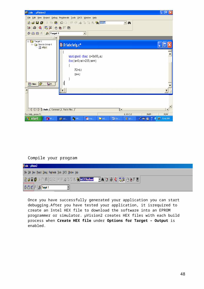
#include<reg51.h>void main(){
unsigned int i,j,k;while(1){
j=0x80;for(i=0;i<4;i++){
P2=j;j=j>>1;for(k=0;k<30000;k++);
}}
}
Assignments
1. Write a program to produce the pattern of SAND GLASS on LED sequence is shown below
1000010000100001100101010011101101111111
2. write a program to blink the LED in bidirectional sequence is shown below
1000010000100001001001001000
6.0 7Segment
The 7 segment display is found in many displays such as microwaves or fancy toaster ovens and occasionally in
48

non cooking devices. It is just 7 LEDs that have been combined into one case to make a convenient device for displaying numbers and some letters. The display is shown on the left. The pin out of the display is on the right.
7 Segment
Writing a character to single 7 Segment
This version is a common anode version. That means that the positive leg of each LED is connected to a common point. Each LED has a negative leg that is connected to one of the pins of the device. To make it work you need to connect pin common to 5 volts trough driver transistor. Then to make each segment light up, connect the ground pin for that led to ground. A resistor is required to limit the current. Rather than using a resistor from each LED to ground, you can just use one resistor from Vcc to pin 3 to limit the current.
Digit a c d e h f b g Hex value
0 0 0 0 0 1 0 0 1 09
1 1 0 1 1 1 1 0 1 BD
2 0 1 0 0 1 1 0 0 4C
3 0 0 0 1 1 1 0 0 1C
4 1 0 1 1 1 0 0 0 B8
5 0 0 0 1 1 0 1 0 1A
6 0 0 0 0 1 0 1 0 0A
7 1 0 0 1 1 1 0 1 9D
8 0 0 0 0 1 0 0 0 08
9 0 0 0 1 1 0 0 0 18
49

6.1 Example-4
Write program to display nine on seven segments
Step 1stBuild the circuit as shown in figure above. As you seen on figure. P1.0 is connected to driver transistor, and each pin of 7 segments is connected to P0.0 trough P0.6. Remember, that all we want to do with this lesson is write a number 1 to 9 in 7 segment.
Step 2ndIn this step, you must write the program in assembly language to display the number on 7 segment, we assume that you have already known the editor, we used MIDE-51 to edit the program.
org 0hstart: mov P0,#18h; send high logic to f and b segment clr P1.0; send current to 7 segment sjmp start; jump forever end
Step 3rdSafe your assembly program above, and name it with 7seg1.asm (for example) Compile the program that you have been save by using keil-u3, see the software instruction.
Step 4thload your hex file (7seg1.hex) into the microcontroller by using Microcontroller flash magic software, see the instruction. After download this hex file you'll see the action of the 7 segment (of course if your cable connection and your program are corrected).
50

6.2 Example-5
WRITE PROGRAM IN ‘C’ TO DISPLAY A NUMBER 1 TO 9 ON SEVEN SEGMENTS
# include<reg51.h>
sbit set1=P1^0;
unsigned char arr[]={0x09,0xbd,0x4c,0x1c,0xb8,0x1a,0x0a,0x9d,0x08,0x18};
main(){
unsigned char i,j,k;
while(1){for(j=0;j<=9;j++)
{for(k=0;k<=100;k++)
{set1=0;P0=arr[j];
}}
}
6.3 Example-6
Step 1stBuild the circuit as shown in figure above. As you seen on figure. P1.0 and P1.1 is connected to driver transistor, and each pin of 7 segments is connected to P0.0 trough P0.6. Remember, that all we want to do with this lesson is write a number counter from 0to 99 into the segment.
51

Step 2ndIn this step, you must type the assembly program to make your 7 segment shown a number on 7 segment, we assume that you have already known the editor, we used keil to edit the program.
org 0hmain: mov r4 , #0ah;
mov p1, #0ffh;mov r2 , #00h;mov dptr , #lookup;
l3: mov r3,#0a0h;mov r1,#00h;
l2: mov r0,#0ffh;
l1: clr p1.0;mov a,r1;movc a,@a+dptr;mov p0,a;acall delay;setb p1.0;clr p1.1;mov a,r2;movc a,@a+dptr;mov p0,a;acall delay;setb p1.1;djnz r0,l1;inc r1;djnz r3,l2;inc r2;djnz r4,l3;sjmp main;
delay: push 00;push 01;
mov r0,#0ffh;l4: mov r1,#1fh;l5: djnz r1,l5;
djnz r0,l4;pop 01;pop 00;ret
0rg 2000hlookup: DB #90h,#0bdh,#4ch,#1ch,#0b8,#1ah,#0ah,#9dh,#08h,#18h
end
Step 3rdSafe your assembly program above, and name it with 7seg1.asm (for example) Compile the program that you have been save by using keil-u3, see the software instruction.
Step 4thload your hex file (7seg2.hex) into the microcontroller by using Microcontroller flash magic software, see the
52

instruction. After download this hex file you'll see the action of the 7 segment (of course if your cable connection and your program are corrected).
6.4 Example-7
Now we will write the same program in c Save the program as 7seg2.c
#include<reg51.h>
sbit seg1=P1^0;sbit seg2=P1^1;
unsigned char arr[]={0x09,0xbd,0x4c,0x1c,0x0b8,0x19,0x0a,0x9d,0x08,0x18};
delay(){
unsigned int k;for(k=0;k<50000;k++);
}
main(){
unsigned char i,j,k;
while(1){
for(i=0;i<10;i++){
for(j=0;j<10;j++){
for(k=0;k<=30;k++){
seg1=0; seg2=1;
P0=arr[i];delay();seg1=1;seg2=0;P0=arr[j];delay();
}}
}}
53

7. LCD Character 2 x 16
The LCD Module can easily be used with an 8051 microcontroller such as the P89V51RD2BN. The LCD Module comes with a 16 pin connector. This can be plugged into connector 16 pin. The pins on the 16 pin connector of the LCD Module are defined below.
Figure LCD Character 2 x 16 Module
PIN Name Function1 VSS Ground voltage
2 VCC +5V3 VEE Contrast voltage
4 RSRegister Select0 = Instruction Register1 = Data Register
5 R/WRead/ Write, to choose write or read mode0 = write mode1 = read mode
6 EEnable0 = start to latch data to LCD character1= disable
7 DB0 LSB
8 DB1 -9 DB2 -
10 DB3 -11 DB4 -
12 DB5 -13 DB6 -
14 DB7 MSB
54

15 BPL Back Plane Light16 GND Ground voltage
7.1 LCD Character Background
The LCD Character standard requires 3 control lines as well as either 4 or 8 I/O lines for the data bus. The user may select whether the LCD is to operate with a 4-bit data bus or an 8-bit data bus. If a 4-bit data bus is used the LCD will require a total of 7 data lines (3 control lines plus the 4 lines for the data bus). If an 8-bit data bus is used the LCD will require a total of 11 data lines (3 control lines plus the 8 lines for the data bus).
The three control lines are referred to as EN, RS, and RW.
EN (enable)
This pin is used by the LCD to latch information presented to its data pin. When you are sending any data high to low pulse ((EN=1) after a short delay (EN=0)) must be send in order to latch the given information.
RS (Register select)
The RS line is the "Register Select" line. When RS is low (0), the data is to be treated as a command or special instruction (such as clear screen, position cursor, etc.). When RS is high (1), the data being sent is text data which should be displayed on the screen. For example, to display the letter "T" on the screen you would set RS high.
R/W (Read /write)
The RW line is the "Read/Write" control line. When RW is low (0), the information on the data bus is being written to the LCD. When RW is high (1), the program is effectively querying (or reading) the LCD. Only one instruction ("Get LCD status") is a read command. All others are write commands--so RW will almost always be low.
Finally, the data bus consists of 4 or 8 lines (depending on the mode of operation selected by the user). In the case of an 8-bit data bus, the lines are referred to as DB0, DB1, DB2, DB3, DB4, DB5, DB6, and DB7.
7.2 An Example Hardware ConfigurationAs we've mentioned, the LCD requires either 8 or 11 I/O lines to communicate with. For the sake of this tutorial, we are going to use an 8-bit data bus--so we'll be using 11 of the 8051's I/O pins to interface with the LCD.
Pin connection between LCD Character to microcontroller
Initializing LCD Character
55

7.3 Function SetSets the interface data length, the number of lines, and character font
RS R/W DB7 DB6 DB5 DB4 DB3 DB2 DB1 DB00 0 0 0 1 DL N F X X
Note : X = Don't care DL : Sets interface data length. DL = 1, Data is sent or received in 8 bit length ( DB7 - DB0 ) DL = 0, Data is sent or received in 4 bit lenght ( DB7 - DB4 ) When the 4 bit length is selected, data must be sent or received twice.
7.4 Entry Mode SetSets the increment/ Decrement and Shift modes to the desired settigs
RS R/W DB7 DB6 DB5 DB4 DB3 DB2 DB1 DB0
0 0 0 0 0 0 0 1 I/D SI/D : Increment/ Decrement the DDRAM address by 1 when a character code is written into or read from the DDRAM I/D = "0", Decrement I/D = "1", IncrementS : Shift the entire display either to the right or to left. S = 1, shift to right or left depend on I/D S = 0, display does not shift
7.5 Display On/ Off CursorControls the display ON/OFF status, cursor ON/OFF and Cursor Blink function
RS R/W DB7 DB6 DB5 DB4 DB3 DB2 DB1 DB00 0 0 0 0 0 1 D C B
D : Controlling display D = 1, Display is ON D = 0, Display is OFF In this case display data remains in the DDRAM. It can be displayed immediately by setting D = 1.C : Display cursor C = 1, Cursor is Displayed C = 0, Cursor does not displayB : The character indicated by the cursor blinks when B=1
7.6 Clear DisplayThe execution of clear display instruction sets entry mode to increment mode
RS R/W DB7 DB6 DB5 DB4 DB3 DB2 DB1 DB00 0 0 0 0 0 0 0 0 1
7.7 Cursor of Display SiftShifts the cursor position or display to the right or left without writing or reading display data. This function is used to correct or search for the display
RS R/W DB7 DB6 DB5 DB4 DB3 DB2 DB1 DB0
56
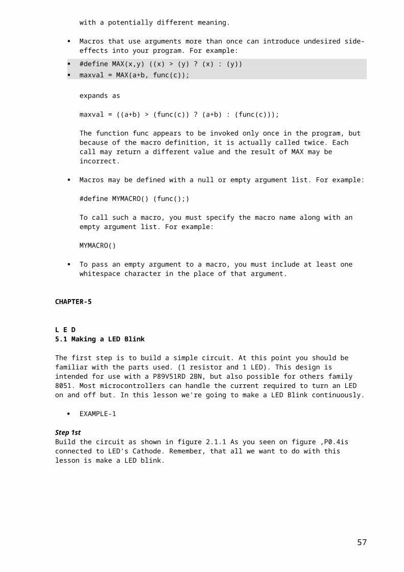
0 0 0 0 0 0 S/C R/L X XNote : x = Don’t care
S/C R/L Note0 0 Shift cursor position to the left
0 1 Shift cursor position to the right1 0 Shift the entire display to the left
1 1 Shift the entire display to the right
7.8 INITIALIZING THE LCD
Before you may really use the LCD, you must initialize and configure it. This is accomplished by sending a number of initialization instructions to the LCD.
The first instruction we send must tell the LCD whether we'll be communicating with it with an 8-bit or 4-bit data bus. We also select a 5x8 dot character font. These two options are selected by sending the command 38h to the LCD as a command. As you will recall from the last section, we mentioned that the RS line must be low if we are sending a command to the LCD. Thus, to send this 38h command to the LCD we must execute the following 8051 instructions:
Here we have used 4bit mode to send data to lcd. To do this we have used four msb lines of lcd to send data as seen in picture.
EXAMPLE-7
Init_lcd: mov A,#00000001b ; Display clear acall write_inst ; mov A,#00111000b ; Function set( Data 8 bit,2 line font 5x7)
acall write_inst ; mov A,#00001100b ; Display on, ;cursor off, cursor blink off acall write_inst mov A,#00000110b ; Entry mode, Set increment acall write_inst ret
Write_inst: clr P1.0; RS=0 to select the command register clr P1.1; RW=0 to write command into the LCD mov B,A; to get data from A to B ANL A,#0F0h to mask the lower 4-bit RR A RR A RR A RR A mov P0,A setb P1.2 ; EN = 1 nop ; call delay time nop clr P1.2 ; EN = 0 mov A,B ANL A,#0Fh Mov P0,A setb P1.2 ; EN = 1 nop ; call delay time nop clr P1.2 ; EN = 0 ret
57

The write_inst routine that we just wrote will send theinstruction to pick the address or initializing.
Write_data: setb P1.0 ; RS = P1.0 = 0, write mode instruction Clr P1.1 ; RW mov B,A ANL A,#0F0h RR A RR A RR A RR A mov P0,A setb P1.2 ; EN = 1 nop ; call delay time nop clr P1.2 ; EN = 0 mov A,B ANL A,#0Fh Mov P0,A setb P1.2 ; EN = 1 nop ; call delay time nop clr P1.2 ; EN = 0 ret The write_data routine that we just wrote will send the character in the accumulator to the LCD which will, in turn, display it. Thus to display text on the LCD all we need to do is load the data in A to P0 that already connected to DB7 – DB4. Pretty easy, huh?
EXAMPLE-7:
writing “WELCOME TO “to LCD Character. Now that we have all the component subroutines written, writing the classic "WELCOME TO" program--which displays the text "WELCOME TO” on the LCD is a relatively trivial matter. Consider
Main: call init_LCD mov A,#80h call write_inst mov A,#'W' call write_data mov A,#'E' call write_data mov A,#'L' call write_data mov A,#'C' call write_data mov A,#'O' call write_data mov A,#'M' call write_data mov A,#'E' call write_data mov A,#'' call write_data mov A,#'T' call write_data mov A,#'O' call write_data
end
58

The above program, should when executed, initiated LCD, choose address DDRAM, and display WELCOME TO upper left hand corner the display.
8.0 Liner key pad:
It means by using any key we have to do any particular work by that key. It is most useful for any sequence generation. Some time it is required to do more than one work by a single switch. Here we have given next two examples to explain.
EXAMPLE-8
Write a program to turn on and off LED with a single switch operation.
Step1: save this program as single_key.asm.
Step2: write this program using keil compiler and debug it. The connection is described as our development kit.
; Key is connected at p2.3 and p2.4
; 4 led's are connected at P0.4 to p0.7; P2.4 must be grounded KEY bit P2.3GND bit P2.4LED_PORT equ P0COUNT1 equ 30hCOUNT2 equ 31h
59

main: mov a, #00hclr GND
back: mov LED_PORT, ajb KEY, backjnb KEY, $acall delaycpl aacall delaysjmp back
delay: mov COUNT1,#0f0hlabel1: mov COUNT2, #0fhlabel2: djnz COUNT2, label2
djnz COUNT1, label1retend
step3: run this in the board.
Now here comes the same program with c. I wish you will now understand the difference between c and assembly.
EXAMPLE-9
Step1: save the program as single_key.cStep2: compile it using keil compiler
/*key is conected at p2.3 and p2.4 4 led's are connected at P0.4 to p0.7P2.4 must be grounded */
#include<reg51.h>
sbit KEY = P2^3;sbit GND=P2^4;sfr LED_PORT = 0x80;
void delay(void);
void main(){
unsigned char ch=0x00;GND=0;while(1){
LED_PORT=ch;if(KEY==0){
while(KEY==0);delay();ch=~ch;
}}
}
60

void delay(){
unsigned char i;for(i=0;i<=200;i++);
}
Write the same program if four switches are connected.
EXAMPLE-10
Step 1:save it as linear.asm
Step2: write the program using keil
;key is conected at p2.3 and p2.4 ;4 led's are connected at P0.4 to p0.7;P2.4 must be grounded
KEY1 bit P2.4KEY2 bit P2.5KEY3 bit P2.6KEY4 bit P2.7GND bit P2.3LED_PORT equ P0COUNT1 equ 30hCOUNT2 equ 31h
main: clr GNDloop: jnb KEY1, sub1
jnb KEY2, sub2jnb KEY3, sub3jnb KEY4, sub4sjmp loop
sub1: jnb KEY1, sub1acall delaymov a,#55hmov P0,aret
sub2: jnb KEY2, sub2acall delaymov a,#0aahmov P0,aret
sub3: jnb KEY3, sub3acall delaymov a,#00hmov P0,aret
sub4: jnb KEY4, sub4acall delaymov a,#0ffhmov P0,aret
delay: mov COUNT1,#0f0hlabel1: mov COUNT2,#0fhlabel2: djnz COUNT2, label2
djnz COUNT1, label1retend
61

EXAMPLE-11
Now the same program with c
/*key is conected at p2.3 and p2.4 4 led's are connected at P0.4 to p0.7P2.4 must be grounded */#include<reg51.h>
sbit KEY1 = P2^4;sbit KEY2 = P2^5;sbit KEY3 = P2^6;sbit KEY4 = P2^7;sbit GND = P2^3;sfr LED_PORT = 0x80;
void delay(void);void sub(unsigned char);
void main(){
GND=0;while(1){
if(KEY1==0)sub(0x55);
if(KEY2==0)sub(0xaa);
if(KEY3==0)sub(0x00);
if(KEY4==0)sub(0xff);
}}
void sub(unsigned char ch){
P0=ch;delay();
}
void delay(){
unsigned char i;for(i=0;i<=200;i++);
}
9.0 K E Y P A D 4 x 4
Keypads are often used as a primary input device for embedded microcontrollers. The keypads actually consist of a number of switches, connected in a row/column arrangement as shown in Fig.
In order for the microcontroller to scan the keypad, it outputs a nibble to force one (only one) of the columns low and then reads the rows to see if any buttons in that column have been pressed. The rows are pulled up by the internal weak pull-ups in the 8051 ports. Consequently, as long as no buttons are pressed, the microcontroller sees a logic high on each of the pins attached to the keypad rows. The nibble driven onto the columns always contains
62

only a single 0. The only way the microcontroller can find a 0 on any row pin is for the keypad button to be pressed that connects the column set to 0 to a row. The controller knows which column is at a 0-level and which row reads 0, allowing it to determine which key is pressed. For the keypad, the pins from left to right are: R1, R2, R3, R4, C1, C2, C3, C4.
Keypad 4 X 4 Connection
The Algorithm
Matrix-type keypads consist of a rectangular array of momentary push button. Each row and each column of push buttons is connected to a common rail. Suppose a four by four array of push button are used. A four by four array is often used to input hexadecimal numbers. There are four column rails and four row rails. Each pushbutton has two terminals, one connected to its column rail and the other to its row rail. The row and column rails are connected to the microcontroller ports. The columns are driven low by output port. The rows are then read into the input ports. If no key is pressed, the rows read 1. When a row is detected to be 0, it indicates that a key in that row is pressed. The task now is to detect which key of the row is actually pressed. The microcontroller loops through each column, driving only one column low at a time as it inspects the row. The microcontroller needs to poll the rows to see if a key is pressed. Only when the column in which the pressed key resides is driven low is the row rail grounded, and thus the voltage is low. The rows and columns are interchangeable, that is, the rows may be driven low as the columns are read by the input ports.
Display Keypad Data to 7-segment
#include<reg51.h>sbit col0=P2^4;sbit col1=P2^5;sbit col2=P2^6;sbit col3=P2^7;sbit row0=P2^3;sbit row1=P2^2;sbit row2=P2^1;sbit row3=P2^0;sbit set1=P1^0;sbit set2=P1^1;
unsigned char arr[]={0x09,0xbd,0x4c,0x1c,0xb8,0x1a,0x0a,0x9d,0x08,0x18};unsigned char ab=0;
void wait (void){
unsigned int i;for(i=0;i<=1000;i++);
}
void scan(){
row0=0;row3=1;if(col0==0){
63

ab=0;}if(col1==0){
ab=1;}if(col2==0){
ab=2;}if(col3==0){
ab=3;}row0=1;row1=0;if(col0==0){
ab=4;}if(col1==0){
ab=5;}if(col2==0){
ab=6;}if(col3==0){
ab=7;}row1=1;row2=0;if(col0==0){
ab=8;}if(col1==0){
ab=9;}if(col2==0){
ab=10;}if(col3==0){
ab=11;}row2=1;row3=0;if(col0==0){
ab=12;}
64

if(col1==0){
ab=13;}if(col2==0){
ab=14;}if(col3==0){
ab=15;}
}
void sevensegment(){
unsigned char p, q;p=ab%10;q=ab/10;set1=0;
set2=1;P0=arr[p];wait ();set1=1;
set2=0;P0=arr[q];wait();
} main(){ P2=0xFF; while(1) { scan(); sevensegment(); }}
Display Keypad Data to LED
In this lesson we are like to design, how to scan keypad 4 x 4, and then display it to LED.
65

Keypad connection and display to LCD
EXAMPLE-12
Step 1stBuild the circuit as shown in figure. As you seen on figure. P2.0 trough P2.7 is connected to keypad 4 x 4 and to drive Lcd, it's connected to P0.4 trough P0.7.
Step 2ndIn this step, you must type the assembly program to scan your keypad data, we assume that you have already known the editor, we used a-51 to edit the program.
#include<reg51.h>
sbit col0=P2^4;sbit col1=P2^5;sbit col2=P2^6;sbit col3=P2^7;sbit row0=P2^3;sbit row1=P2^2;sbit row2=P2^1;sbit row3=P2^0;
sfr LCD_DATA=0x80;sbit LCD_RS=P1^0;sbit LCD_RW=P1^1;sbit LCD_EN=P1^2;#define LCD_STROBE() ((LCD_EN = 1),(LCD_EN=0))
void wait(void){
unsigned int i;for(i=0;i<=1000;i++);
}
/*void delay(unsigned int dd){
unsigned int d,ddd;
66

for(ddd=0;ddd<dd;ddd++)for(d=0;d<100;d++);
} */
void lcd_write(unsigned char cd){
unsigned char cl,ch,j;ch=cd&0xf0;ch=ch>>4; depend if we need to shift dataLCD_DATA=(ch|0xf0);LCD_STROBE();for(j=0;j<=100;j++);cl=cd&0x0f;LCD_DATA=(cl|0xf0);LCD_STROBE();
}
void lcd_init(void){
LCD_RW=0;LCD_RS=0;wait();lcd_write(0x33);wait();lcd_write(0x32);wait();lcd_write(0x28);wait();
// lcd_write(0x38);// wait();
lcd_write(0x08);wait();lcd_write(0x01);wait();lcd_write(0x06);wait();lcd_write(0x0e);wait();
}
key_init(){
P2=0xff;}
unsigned char scan(){while(1){
row0=0;row3=1;if(col0==0){
while(col0==0);wait();return('1');
}if(col1==0){
while(col1==0);wait();return('2');
}if(col2==0){
while(col2==0);
67

wait();return('3');
}if(col3==0){
while(col3==0);wait();return('4');
}row0=1;row1=0;if(col0==0){
while(col0==0);wait();return('5');
}if(col1==0){
while(col1==0);wait();return('6');
}if(col2==0){
while(col2==0);wait();return('7');
}if(col3==0){
while(col3==0);wait();return('8');
}row1=1;row2=0;if(col0==0){
while(col0==0);wait();return('9');
}if(col1==0){
while(col1==0);wait();return('a');
}if(col2==0){
while(col2==0);wait();return('b');
}if(col3==0){
while(col3==0);wait();return('c');
}row2=1;row3=0;if(col0==0){
while(col0==0);
68

wait();return('d');
}if(col1==0){
while(col1==0);wait();return('e');
}if(col2==0){
while(col2==0);wait();return('f');
}if(col3==0){
while(col3==0);wait();return('0');
}}}
void lcd_goto(unsigned char pos){
LCD_RS=0;wait();
lcd_write(0x80+pos);wait();//LCD_RS=1;
}
void lcd_clear(void){
LCD_RS=0;lcd_write(0x01);
}
void lcd_putch(char ch){
LCD_RS=1;wait();lcd_write(ch);
}
void lcd_putstr(const char *str,char c){
char l;LCD_RS=1;for(l=0;l<c;l++){
wait();lcd_write(*str++);}
}
main(){
unsigned char cr;lcd_init();key_init();lcd_clear();lcd_goto(0x04);lcd_putstr("Wellcome",8);lcd_goto(0x40);
69

while(1){
cr=scan();lcd_putch(cr);
}}
Step 3rdSave your program above, and name it with key1.c (for example) Compile the program that you have been save by using KEIL, see the software instruction.
Step 4thDownload your hex file (key1.hex) into the microcontroller by using Microcontroller ISP software, see the instruction. After download this hex file you'll see the action of Keypad 4 x 4(of course if your cable connection and your program are corrected )
10 STEPPER MOTOR
Driving Stepper Motor
General Theory of Stepper Motors
An ordinary DC motor will turn around and around as long as power is supplied. No intelligent circuitry is required to drive such a motor, unless you want to slow it down or reverse direction - just apply power and it spins. A stepper motor is very different. If you just feed it power, it will stay where it is. In order to make the motor move, you have to feed it a changing signal. This is best illustrated by thinking of a magnetic compass with electromagnets around it:
Motor Stepper
The drawing on the bottom shows power applied to the N electromagnet, drawing the compass toward it. On the right, power is instead applied to the E electromagnet, and the needle has rotated toward that side.
70

Basic Stepper Motor
Just four electromagnets would give coarse jumpy motion. Now imagine a similar arrangement with 100 electromagnets around the compass. By energizing each electromagnet in sequence, the needle takes 100 steps around the circle. But driving 100 individual electromagnets would require complex electronics. We fake it:
Basic Motor Stepper with more electromagnet
In these drawing, the circled letters represent electromagnets. All the magnets with the same letter are wired together. When you energize that circuit, all of the electromagnets torn on at once. On the left, there are 8 magnets, but only 4 circuits. Sequencing through the four circuits gives half of a rotation. One more run through the sequence completes the rotation. This setup requires that both ends of the compass needle be north-seeking. On the right, the same 4 circuits energize 16 magnets. This setup requires 16 steps (4 repetitions of a 4-step cycle) to complete one rotation.
On the right, the same 4 circuits energize 16 magnets. This setup requires 16 steps (4 repetitions of a 4-step cycle) to complete one rotation. In actual practice, just four control wires can provide just about as many steps as you might want. One of the characteristics of a given stepper motor is the number of steps necessary to make a complete circle, usually expressed as number of degrees per step.
Full Step Mode
A B C D Comment
1 0 0 0 Take a step clock wise0 1 0 0 another step clock wise
0 0 1 0 another step clock wise0 0 0 1 another step clock wise
0 0 0 1 No step take0 0 1 0 Take a step back
More Complex DriveAs we have seen, it is very easy to drive a stepper motor, by simply turning one electromagnet fully on at a time. But there are other ways to drive a stepper motor.
Half StepsBy turning on two coils at once, the motor will take a position between the two steps.
71

A B C D Comment1 0 0 0 Take a step clock wise
1 1 0 0 Half a step clock wise
0 1 0 0 The complete full step clock wise
0 1 1 0 another half step clock wise0 0 1 0 The complete full step clock wise
0 0 1 1 Another half step clock wise0 0 0 1 The complete full step clock wise
1 0 0 1 another half step clock wise1 0 0 0 Start position
EXAMPLE-13
Step1: set the stepper motor as seen as above figure. Here we have used 8 step sequences to rotate the motor.
Step2: now write the program for the same and save as stepper.asm.
COUNT1 equ 30hCOUNT2 equ 31h
org 0000hmain: mov dptr,#lookup ;lookup moves to dptr
mov r1,#08h ;for 8step sequencemov r0,#00h
loop: mov a,r0movc a,@a+dptr ;value of dptr moves to Amov P2,aacall delayinc r0djnz r1,loopsjmp loop
delay: mov COUNT1,#0f0hlabel1: mov COUNT2,#0fhlabel2: djnz COUNT2, label2djnz COUNT1, label1
ret
org 1000h
72
lookup: db 90h,80h,0c0h,40h,60h,40h,30h,10hend
step3: compile it and create hex file.
EXAMPLE-14
Now we will write the same program with embedded c
Step1: save the program as stepper.c
Step2: write the program and compile with C-51 compiler.
#include<reg51.h>
unsigned char step_arr[]={0x90,0x80,0xc0,0x40,0x60,0x30,0x10};
void delay(void);
void main(){
unsigned char j;while(1){
for(j=0;j<=7;j++){
P2=step_arr[j];delay();
}}
}
void delay(){
unsigned int i;for(i=0;i<=1000;i++);
}
Step3: create hex file and run it.
11.0 Interrupt
The 80C51 provides 5 interrupt sources. These are shown below. The External Interrupts INT0 and INT1 can each be either level-activated or transition-activated, depending on bits IT0 and IT1 in Register TCON. The flags that actually generate these interrupts are bits IE0 and IE1 in TCON. When an external interrupt is generated, the flag that generated it is cleared by the hardware when the service routine is vectored to only if the interrupt was transition-activated. If the interrupt was level-activated, then the external requesting source is what controls the request flag, rather than the on-chip hardware.
The Timer 0 and Timer 1 Interrupts are generated by TF0 and TF1, which are set by a rollover in their respective Timer/Counter registers (except see Timer 0 in Mode 3). When a timer interrupt is generated, the flag that generated it is cleared by the on-chip hardware when the service routine is vectored to.
73

The Serial Port Interrupt is generated by the logical OR of RI and TI. Neither of these flags is cleared by hardware when the service routine is vectored to. In fact, the service routine will normally have to determine whether it was RI or TI that generated the interrupt, and the bit will have to be cleared in software.
All of the bits that generate interrupts can be set or cleared by software, with the same result as though it had been set or cleared by hardware. That is, interrupts can be generated or pending interrupts can be canceled in software.
Each of these interrupt sources can be individually enabled or disabled by setting or clearing a bit in Special Function Register IE. IE also contains a global disable bit, EA, which disables all interrupts at once.
11.1 Priority Level StructureEach interrupt source can also be individually programmed to one of two priority levels by setting or clearing a bit in Special Function
Register IP (Figure 19). A low-priority interrupt can itself be interrupted by a high-priority interrupt, but not by another low-priority interrupt. A high-priority interrupt can’t be interrupted by any other interrupt source.
If two request of different priority levels are received simultaneously, the request of higher priority level is serviced. If requests of the same priority level are received simultaneously, an internal polling sequence determines which request is serviced. Thus within each priority level there is a second priority structure determined by the polling sequence as follows:
11.2 Source Priority Within Level1. IE0 (highest)2. TF03. IE14. TF15. RI+TI (lowest)
Note that the “priority within level” structure is only used to resolve simultaneous requests of the same priority level. The IP register contains a number of unimplemented bits. IP.7, IP.6, and IP.5 are reserved in the 80C51. User software should not write 1s to these positions, since they may be used in other 8051 Family products.
11.3 Interrupt Enable Registe ( IE )
MSB LSBEA X X ES ET1 EX1 ET0 EX0
BIT SYMBOL FUNCTION
IE.7 EADisables all interrupts. If EA=0, no interrupt will be acknowledged. If EA=1, each interrupt source is individually enabled or disabled by setting or clearing its enable bit.
IE.6 - -
IE.5 - -
IE.4 ES Enables or disables the Serial Port interrupt. If ES=0, the Serial Port interrupt is disabled.
IE.3 ET1 Enables or disables the Timer 1 Overflow interrupt. If ET1=0, the Timer 1 interrupt is disabled.
74

IE.2 EX1 Enables or disables External Interrupt 1. If EX1=0, External interrupt 1 is disabled.
IE.1 ET0 Enables or disables the Timer 0 Overflow interrupt. If ET0=0, the Timer 0 interrupt is disabled.
IE.0 EX0 Enables or disables External interrupt 0. If EX0=0, External interrupt 0 is disabled.
11.4 Interrupt Priority Register ( IP )
MSB LSB
X X X PS PT1 PX1 PT0 PX0
Note:BIT SYMBOL FUNCTIONIP.7 - -IP.6 - -
IP.5 - -
IP.4 PS Defines the Serial Port interrupt priority level. PS=1 programs it to the higher priority level.
IP.3 PT1 Defines the Timer 1 interrupt priority level. PT1=1 programs it to the higher priority level.
IP.2 PX1 Defines the External Interrupt 1 priority level. PX1=1 programs it to the higher priority level.
IP.1 PT0 Enables or disables the Timer 0 interrupt priority level. PT0=1 programs it to the higher priority level.
IP.0 PX0 Defines the External Interrupt 0 priority level. PX0=1 programs it to the higher priority level.
Source Vector AddressIE0 0003HTF0 000BH
IE1 0013HTF1 001BH
RI + TI 0023H
EXAMPLE-15
Write a program that continuously gets 8-bit data from P0 and sends it to P1 while simultaneously creating a square wave of 200 µs period on pin P2.1. Use timer 0 to create the square wave. Assume that XTAL=11.0592 MHz.
Solution:
; we will use timer 0 mode 2 . TH0= 100/1.085us=92
org 0000h ljmp main org 000bhcpl p2.1reti
75

org 0030h
main: mov TMOD ,#02hmov p0,#0ffhmov TH0,#-92mov IE,#82h ;enable timer0setb tr0 ; start timero
back; mov a,p0mov p1,asjmp back
end
EXAMPLE-16]
WAP using interrupt to do the following
(A) display the continuously shifting of LED(B) when row0 and coloumn0 is pressed it increment the count and if row0 and column1 is pressed it
decrement the count.
#include<reg51.h>sbit set1=P1^0;sbit set2=P1^1;sbit col0=P2^4;sbit row0=P2^3;sbit col1=P2^5;
unsigned char arr[]={0x09,0xbd,0x4c,0x1c,0xb8,0x1a,0x0a,0x9d,0x08,0x18};unsigned char count=0,p=0,q=0,cnt=0;bit b=0;
wait(){
unsigned int k;for(k=0;k<1000;k++);
}
void port(void) interrupt 3{
if(!b){TR1=0;
if(col0==0){
count=count+1;p=count%10;q=count/10;b=1;
}if (col1==0){
count=count-1;p=count%10;q=count/10;b=1;
}TF1=0;
76
TL0=0x00;TH0=0x00;TR1=1;
}else{
if(cnt<=100)cnt++;
elseb=0;
} }
main(){
unsigned int i,j;unsigned char ch;row0=0;TMOD=0x10;IE=0x88; /*timer1 interrupt is used*/TL1=0x00;TH1=0x00;TR1=1;TF1=0;
while(1){
ch=0x01;for(i=0;i<8;i++)
{P3=ch;ch<<=1;for(j=0;j<=100;j++){
set1=0;set2=1;P0=arr[p];wait();set1=1;set2=0;P0=arr[q];wait();
} }
}
}
write a c program using interrupts to do the following:
a) Receive data serially and send it to P1b) read port P1, transmit data serially and give a copy to P2c) make timer 0 generate a square wave of 5Khz frequency on P0.1 set baud rate at 4800
solution:
77

#include<reg51.h>sbit wave = P0^1;
void timer0() intrrupt 1 {
wave= ~wave;
}
void serial0() intrrupt 4 {
if(TI == 1) { TI = 0; }else { P0 = SBUF; RI = 0; }
}
void main() { unsigned char x; P1 = 0xFF;
TMOD = 0X22;TH1 = 0XF6; // 4800 BAUD RATE SCON = 0X50;TH0 = 0XA4;IE = 0X92;TR1 = 1;TR0 = 1;
while(1) {
x= P1;SBUF = X;P2 = X;
} }
78

12 Standard Serial Interface
The serial port is full duplex, meaning it can transmit and receive simultaneously. It is also receive-buffered, meaning it can commence reception of a second byte before a previously received byte has been read from the register. (However, if the first byte still hasn’t been read by the time reception of the second byte is complete, one of the bytes will be lost.) The serial port receive and transmit registers are both accessed at Special Function Register SBUF. Writing to SBUF loads the transmit register, and reading SBUF accesses a physically separate receive register.
Standard serial communication
12.1 The serial port can operate in 4 modes:
Mode 0: Serial data enters and exits through RxD. TxD outputs the shift clock. 8 bits are transmitted/received (LSB first). The baud rate is fixed at 1/12 the oscillator frequency.
Mode 1: 10 bits are transmitted (through TxD) or received (through RxD): a start bit (0), 8 data bits (LSB first), and a stop bit (1). On receive, the stop bit goes into RB8 in Special Function Register SCON. The baud rate is variable.
Mode 2: 11 bits are transmitted (through TxD) or received (through RxD): start bit (0), 8 data bits (LSB first), a programmable 9th data bit, and a stop bit (1). On Transmit, the 9th data bit (TB8 in SCON) can be assigned the value of 0 or 1. Or, for example, the parity bit (P, in the PSW) could be moved into TB8. On receive, the 9th data bit goes into RB8 in Special Function Register SCON, while the stop bit is ignored. The baud rate is
79

programmable to either 1/32 or 1/64 the oscillator frequency.
Mode 3: 11 bits are transmitted (through TxD) or received (through RxD): a start bit (0), 8 data bits (LSB first), a programmable 9th data bit, and a stop bit (1). In fact,Mode 3 is the same as Mode 2 in all respects except baud rate. The baud rate in Mode 3 is variable.
In all four modes, transmission is initiated by any instruction that uses SBUF as a destination register. Reception is initiated in Mode 0 by the condition RI = 0 and REN = 1. Reception is initiated in the other modes by the incoming start bit if REN = 1.
12.2 Serial Port Control RegisterThe serial port control and status register is the Special Function Register SCON, shown in Figure 11. This register contains not only the mode selection bits, but also the 9th data bit for transmit and receive (TB8 and RB8), and the serial port interrupt bits (TI and RI).
12.3 Baud RatesThe baud rate in Mode 0 is fixed: Mode 0 Baud Rate = Oscillator Frequency / 12. The baud rate in Mode 2 depends on the value of bit SMOD in Special Function Register PCON. If SMOD = 0 (which is the value on reset), the baud rate is 1/64 the oscillator frequency. If SMOD = 1, the baud rate is 1/32 the oscillator frequency. Baud Rate mode 2:
,In the 80C51, the baud rates in Modes 1 and 3 are determined by the Timer 1 overflow rate.
12.4 Using Timer 1 to Generate Baud RatesWhen Timer 1 is used as the baud rate generator, the baud rates in Modes 1 and 3 are determined by the Timer 1 overflow rate and the value of SMOD as follows: Baud Rate Mode 1,3
The Timer 1 interrupt should be disabled in this application. The Timer itself can be configured for either “timer” or “counter” operation, and in any of its 3 running modes. In the most typical applications, it is configured for “timer” operation, in the auto-reload mode (high nibble of TMOD = 0010B). In that case the baud rate is given by the formula: Baud Rate Mode 1,3
One can achieve very low baud rates with Timer 1 by leaving the Timer 1 interrupt enabled, and configuring the Timer to run as a 16-bit timer (high nibble of TMOD = 0001B), and using the Timer 1 interrupt to do a 16-bit software reload. Figure 12 lists various commonly used baud rates and how they can be obtained from Timer 1.
12.5 Serial Port Control ( SCON ) Register
MSB LSB
SM0 SM1 SM2 REN TB8 RB8 TI RI
Where SM0, SM1 specify the serial port mode, as follows
SM0 SM1 Mode Description Baud Rate0 0 0 Shif Register fosc/ 120 1 1 8 bit UART variable
1 0 2 9 bit UART fosc/64 fosc/321 1 3 9 bit UART variable
80

Note:
SM2
Enables the multiprocessor communication feature in Modes 2 and 3. In Mode 2 or 3, if SM2 is set to 1, then Rl will not be activated if the received 9th data bit (RB8) is 0. In Mode 1, if SM2=1 then RI will not be activated if a valid stop bit was not received. In Mode 0, SM2 should be 0.
REN Enables serial reception. Set by software to enable reception. Clear by software to disable reception.
TB8 The 9th data bit that will be transmitted in Modes 2 and 3. Set or clear by software as desired.
RB8In Modes 2 and 3, is the 9th data bit that was received. In Mode 1, it SM2=0, RB8 is the stop bit that was received. In Mode 0,RB8 is not used.
TITransmit interrupt flag. Set by hardware at the end of the 8th bit time in Mode 0, or at the beginning of the stop bit in the other modes, in any serial transmission. Must be cleared by software.
RIReceive interrupt flag. Set by hardware at the end of the 8th bit time in Mode 0, or halfway through the stop bit time in the other modes, in any serial reception (except see SM2). Must be cleared by software.
Here we are able to calculate a nice, even TH1 value. Therefore, to obtain 19,200 baud with an 11.059MHz crystal we must:
1. Configure Serial Port mode 1 or 3.
2. Configure Timer 1 to timer mode 2 (8-bit auto-reload).
3. Set TH1 to 253 to reflect the correct frequency for 19,200 baud.
4. Set PCON.7 (SMOD) to double the baud rate.
12.6 Writing to the Serial Port
Once the Serial Port has been properly configured as explained above, the serial port is ready to be used to send data and receive data. If you thought that configuring the serial port was simple, using the serial port will be a breeze. To write a byte to the serial port one must simply write the value to the SBUF (99h) SFR. For example, if you wanted to send the letter "A" to the serial port, it could be accomplished as easily as: MOV SBUF,#A Upon execution of the above instruction the 8051 will begin transmitting the character via the serial port. Obviously transmission is not instantaneous--it takes a measurable amount of time to transmit. And since the 8051 does not have a serial output buffer we need to be sure that a character is completely transmitted before we try to transmit the next character. The 8051 lets us know when it is done transmitting a character by setting the TI bit in SCON. When this bit is set we know that the last character has been transmitted and that we may send the next character, if any. Consider the following code segment: CLR TI ;Be sure the bit is initially clearMOV SBUF,#A ;Send the letter A to the serial portJNB TI,$ ;Pause until the TI bit is set.
The above three instructions will successfully transmit a character and wait for the TI bit to be set before continuing. The last instruction says "Jump if the TI bit is not set to $"--$, in most assemblers, means "the same address of the current instruction." Thus the 8051 will pause on the JNB instruction until the TI bit is set by the 8051 upon successful transmission of the character.
12.7 Reading the Serial Port
81

Reading data received by the serial port is equally easy. To read a byte from the serial port one just needs to read the value stored in the SBUF (99h) SFR after the 8051 has automatically set the RI flag in SCON. For example, if your program wants to wait for a character to be received and subsequently read it into the Accumulator, the following code segment may be used:
JNB RI,$ ;Wait for the 8051 to set the RI flagMOV A,SBUF ;Read the character from the serial port
The first line of the above code segment waits for the 8051 to set the RI flag; again, the 8051 sets the RI flag automatically when it receives a character via the serial port. So as long as the bit is not set the program repeats the "JNB" instruction continuously. Once the RI bit is set upon character reception the above condition automatically fails and program flow falls through to the "MOV" instruction which reads the value.
What Happens When an Interrupt Ends?An interrupt ends when your program executes the RETI (Return from Interrupt) instruction. When the RETI instruction is executed the following actions are taken by the microcontroller:
Two bytes are popped off the stack into the Program Counter to restore normal program execution. Interrupt status is restored to its pre-interrupt status.
12.8 The following table lists the commonly used RS-232 signals and common pin assignments
Signal Type DB-25
DE-9 (TIA-574)
Common Ground 7 5
Transmitted Data 2 3
Received Data 3 2
Data Terminal Ready 20 4
Data Set Ready 6 6
Request To Send 4 7
Clear To Send 5 8
Carrier Detect 8 1
Ring Indicator 22 9
EXAMPLE-16
org 2000h
main: mov tmod,#20h ;timer 1 mode 2mov th1,#-3 ;9600 baud ratemov scon,#50h ;8 bit, 1 stop bit, REN enablesetb TR1mov dptr,#myadatamov r0,#09h
again: clr a movc a,@a+dptr
acall transferinc dptrdjnz r0, again
82

sjmp main
transfe:mov sbuf, al1: jnb TI,l1 clr TI ret
mydata: DB "Innovative labs" end EXAMPLE-17 now we will write the program with c.
#include<reg51.h>
void main (void)
{ unsigned char z;
unsigned char name[]="Innovative labs";TMOD=0x20;TH1=0xfd;SCON=0X50;TR1=1;
for(z=0;z<10;z++)
{ SBUF=name[z];
while(TI==0); TI=0;
}}
WAP using interrupt to display the number 0 to 9 written from keyboard
#include<reg51.h>sbit set1=P1^0;sbit set2=P1^1;unsigned char arr[]={0x09,0xbd,0x4c,0x1c,0xb8,0x1a,0x0a,0x9d,0x08,0x18};unsigned char mybite=0;void serial(void) interrupt 4{
if(RI){
RI=0;mybite=SBUF;
}}
void main(){
TMOD=0x20;TH1=0xFD;SCON=0x50;IE=0x90;TR1=1;while(1){
mybite=mybite&0x0f;set1=0;
set2=1;P0=arr[mybite];
}}
83

13.Timer
The 8051 comes equipped with two timers, both of which may be controlled, set, read, and configured individually. The 8051 timers have three general functions: 1) Keeping time and/or calculating the amount of time between events, 2) Counting the events themselves, or 3) Generating baud rates for the serial port. The three timer uses are distinct so we will talk about each of them separately. The first two uses will be discussed in this chapter while the use of timers for baud rate generation will be discussed in the chapter relating to serial ports. 13.1 How does a timer count?How does a timer count? The answer to this question is very simple: A timer always counts up. It doesnt matter whether the timer is being used as a timer, a counter, or a baud rate generator: A timer is always incremented by the microcontroller.
Programming Tip: Some derivative chips actually allow the program to configure whether the timers count up or down. However, since this option only exists on some derivatives it is beyond the scope of this tutorial which is aimed at the standard 8051. It is only mentioned here in the event that you absolutely need a timer to count backwards, you will know that you may be able to find an 8051-compatible microcontroller that does it.
13.2 Timer SFRsAs mentioned before, the 8051 has two timers which each function essentially the same way. One timer is TIMER0 and the other is TIMER1. The two timers share two SFRs (TMOD and TCON) which control the timers, and each timer also has two SFRs dedicated solely to itself (TH0/TL0 and TH1/TL1). We have given SFRs names to make it easier to refer to them, but in reality an SFR has a numeric address. It is often useful to know the numeric address that corresponds to an SFR name. The SFRs relating to timers are:
SFR Name Description SFR Address
TH0 Timer 0 High Byte 8Ch
TL0 Timer 0 Low Byte 8Ah
TH1 Timer 1 High Byte 8Dh
TL1 Timer 1 Low Byte 8Bh
TCON Timer Control 88h
TMOD Timer Mode 89h
When you enter the name of an SFR into an assembler, it internally converts it to a number. For example, the command:
MOV TH0,#25h moves the value 25h into the TH0 SFR. However, since TH0 is the same as SFR address 8Ch this command is equivalent to:
MOV 8Ch,#25h Now, back to the timers. First, lets talk about Timer 0. Timer 0 has two SFRs dedicated exclusively to itself: TH0 and TL0. Without making things too complicated to start off with, you may just think of this as the high and low byte of the timer. That is to say, when Timer 0 has a value of 0, both TH0 and TL0 will contain 0. When Timer 0 has the value 1000, TH0 will hold the high byte of the value (3 decimal) and TL0 will contain the low byte of the value (232 decimal). Reviewing low/high byte notation, recall that you must multiply the high byte by 256 and add the low byte to calculate the final value. That is to say:
TH0 * 256 + TL0 = 10003 * 256 + 232 = 1000
Timer 1 works the exact same way, but its SFRs are TH1 and TL1. Since there are only two bytes devoted to the value of each timer it is apparent that the maximum value a timer may have is 65,535. If a timer contains the value 65,535 and is subsequently incremented, it will reset--or overflow--back to 0.
13.3 The TMOD SFRLets first talk about our first control SFR: TMOD (Timer Mode). The TMOD SFR is used to control the mode of operation of both timers. Each bit of the SFR gives the microcontroller specific information concerning how to run a timer. The high four bits (bits 4 through 7) relate to Timer 1 whereas the low four bits (bits 0 through 3) perform the exact same functions, but for timer 0.
84
The individual bits of TMOD have the following functions: TMOD (89h) SFR Bit Name Explanation of Function Timer
7 GATE1When this bit is set the timer will only run when INT1 (P3.3) is high. When this bit is clear the timer will run regardless of the state of INT1.
1
6 C/T1When this bit is set the timer will count events on T1 (P3.5). When this bit is clear the timer will be incremented every machine cycle.
1
5 T1M1 Timer mode bit (see below) 1
4 T1M0 Timer mode bit (see below) 1
3 GATE0When this bit is set the timer will only run when INT0 (P3.2) is high. When this bit is clear the timer will run regardless of the state of INT0.
0
2 C/T0When this bit is set the timer will count events on T0 (P3.4). When this bit is clear the timer will be incremented every machine cycle.
0
1 T0M1 Timer mode bit (see below) 0
0 T0M0 Timer mode bit (see below) 0
As you can see in the above chart, four bits (two for each timer) are used to specify a mode of operation. The modes of operation are:
TxM1 TxM0 Timer Mode Description of Mode
0 0 0 13-bit Timer.
0 1 1 16-bit Timer
1 0 2 8-bit auto-reload
1 1 3 Split timer mode
13-bit Time Mode (mode 0)Timer mode "0" is a 13-bit timer. This is a relic that was kept around in the 8051 to maintain compatability with its predecesor, the 8048. Generally the 13-bit timer mode is not used in new development. When the timer is in 13-bit mode, TLx will count from 0 to 31. When TLx is incremented from 31, it will "reset" to 0 and increment THx. Thus, effectively, only 13 bits of the two timer bytes are being used: bits 0-4 of TLx and bits 0-7 of THx. This also means, in essence, the timer can only contain 8192 values. If you set a 13-bit timer to 0, it will overflow back to zero 8192 machine cycles later. Again, there is very little reason to use this mode and it is only mentioned so you wont be surprised if you ever end up analyzing archaeic code which has been passed down through the generations (a generation in a programming shop is often on the order of about 3 or 4 months). 16-bit Time Mode (mode 1)Timer mode "1" is a 16-bit timer. This is a very commonly used mode. It functions just like 13-bit mode except that all 16 bits are used. TLx is incremented from 0 to 255. When TLx is incremented from 255, it resets to 0 and causes THx to be incremented by 1. Since this is a full 16-bit timer, the timer may contain up to 65536 distinct values. If you set a 16-bit timer to 0, it will overflow back to 0 after 65,536 machine cycles.
TOP8-bit Time Mode (mode 2)Timer mode "2" is an 8-bit auto-reload mode. What is that, you may ask? Simple. When a timer is in mode 2, THx holds the "reload value" and TLx is the timer itself. Thus, TLx starts counting up. When TLx reaches 255 and is subsequently incremented, instead of resetting to 0 (as in the case of modes 0 and 1), it will be reset to the value stored in THx.
85

For example, lets say TH0 holds the value FDh and TL0 holds the value FEh. If we were to watch the values of TH0 and TL0 for a few machine cycles this is what wed see:
Machine Cycle TH0 Value TL0 Value
1 FDh FEh
2 FDh FFh
3 FDh FDh
4 FDh FEh
5 FDh FFh
6 FDh FDh
7 FDh FEh
As you can see, the value of TH0 never changed. In fact, when you use mode 2 you almost always set THx to a known value and TLx is the SFR that is constantly incremented. Whats the benefit of auto-reload mode? Perhaps you want the timer to always have a value from 200 to 255. If you use mode 0 or 1, you would have to check in code to see if the timer had overflowed and, if so, reset the timer to 200. This takes precious instructions of execution time to check the value and/or to reload it. When you use mode 2 the microcontroller takes care of this for you. Once you have configured a timer in mode 2 you dont have to worry about checking to see if the timer has overflowed nor do you have to worry about resetting the value--the microcontroller hardware will do it all for you. The auto-reload mode is very commonly used for establishing a baud rate which we will talk more about in the Serial Communications chapter.
Split Timer Mode (mode 3)
Timer mode "3" is a split-timer mode. When Timer 0 is placed in mode 3, it essentially becomes two separate 8-bit timers. That is to say, Timer 0 is TL0 and Timer 1 is TH0. Both timers count from 0 to 255 and overflow back to 0. All the bits that are related to Timer 1 will now be tied to TH0. While Timer 0 is in split mode, the real Timer 1 (i.e. TH1 and TL1) can be put into modes 0, 1 or 2 normally--however, you may not start or stop the real timer 1 since the bits that do that are now linked to TH0. The real timer 1, in this case, will be incremented every machine cycle no matter what. The only real use I can see of using split timer mode is if you need to have two separate timers and, additionally, a baud rate generator. In such case you can use the real Timer 1 as a baud rate generator and use TH0/TL0 as two separate timers.
13.4 The TCON SFRFinally, there’s one more SFR that controls the two timers and provides valuable information about them. The TCON SFR has the following structure:
TCON (88h) SFR
Bit Name Bit Address Explanation of Function Timer
7 TF1 8Fh Timer 1 Overflow. This bit is set by the microcontroller when Timer 1 overflows. 1
6 TR1 8Eh Timer 1 Run. When this bit is set Timer 1 is turned on. When this bit is clear Timer 1 is off. 1
5 TF0 8Dh Timer 0 Overflow. This bit is set by the microcontroller when Timer 0 overflows. 0
4 TR0 8Ch Timer 0 Run. When this bit is set Timer 0 is turned on. When this bit is clear Timer 0 is off. 0
As you may notice, we have only defined 4 of the 8 bits. That is because the other 4 bits of the SFR don’t have anything to do with timers--they have to do with Interrupts and they will be discussed in the chapter that addresses interrupts. A new piece of information in this chart is the column "bit address." This is because this SFR is "bit-addressable." What does this mean? It means if you want to set the bit TF1--which is the highest bit of TCON--you could execute the command:
86
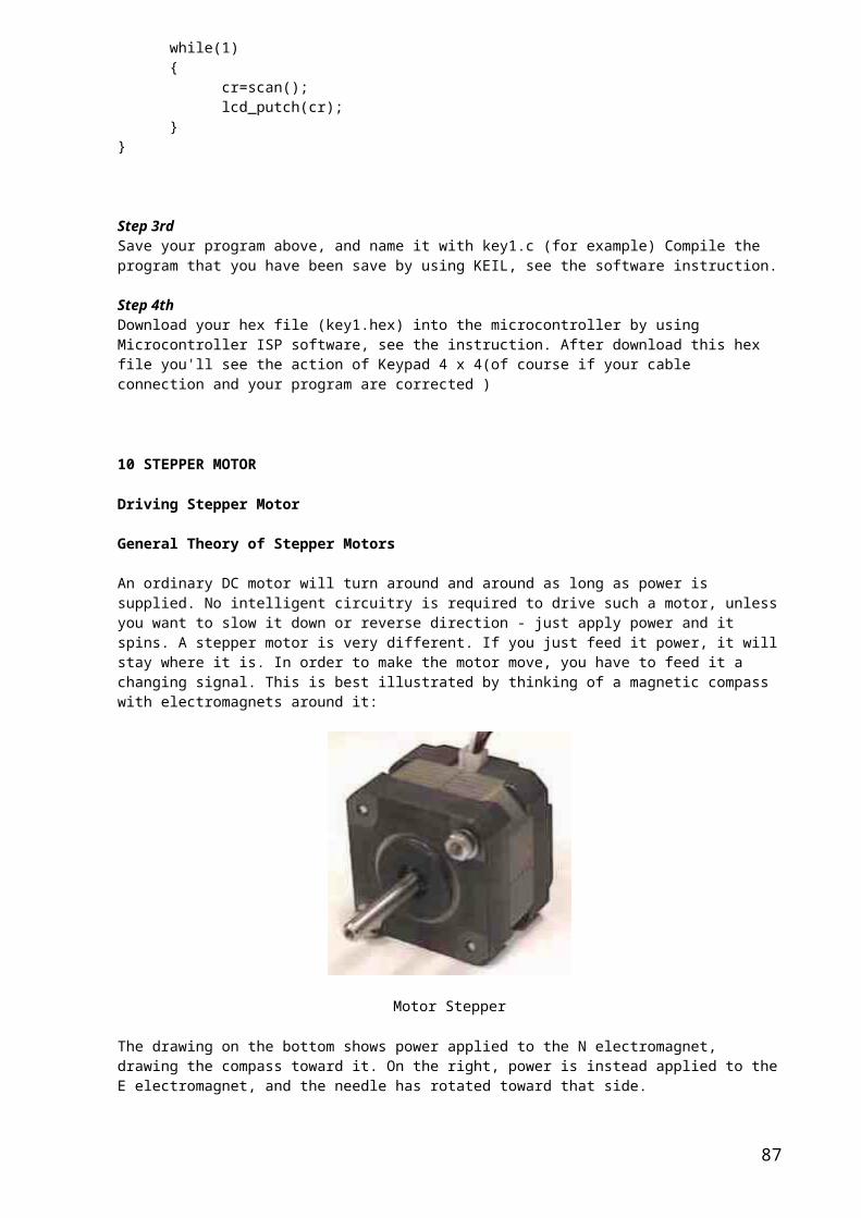
MOV TCON, #80h ... or, since the SFR is bit-addressable, you could just execute the command:
SETB TF1 This has the benefit of setting the high bit of TCON without changing the value of any of the other bits of the SFR. Usually when you start or stop a timer you don’t want to modify the other values in TCON, so you take advantage of the fact that the SFR is bit-addressable.
13.5 Initializing a TimerNow that we have discussed the timer-related SFRs we are ready to write code that will initialize the timer and start it running. As you’ll recall, we first must decide what mode we want the timer to be in. In this case we want a 16-bit timer that runs continuously; that is to say, it is not dependent on any external pins. We must first initialize the TMOD SFR. Since we are working with timer 0 we will be using the lowest 4 bits of TMOD. The first two bits, GATE0 and C/T0 are both 0 since we want the timer to be independent of the external pins. 16-bit mode is timer mode 1 so we must clear T0M1 and set T0M0. Effectively, the only bit we want to turn on is bit 0 of TMOD. Thus to initialize the timer we execute the instruction:
MOV TMOD, #01h Timer 0 is now in 16-bit timer mode. However, the timer is not running. To start the timer running we must set the TR0 bit we can do that by executing the instruction:
SETB TR0 Upon executing these two instructions timer 0 will immediately begin counting, being incremented once every machine cycle (every 12 crystal pulses).
Timing the length of eventsThe 8051 provides another cool toy that can be used to time the length of events. For example, let's say we're trying to save electricity in the office and we're interested in how long a light is turned on each day. When the light is turned on, we want to measure time. When the light is turned off we don't. One option would be to connect the light switch to one of the pins, constantly read the pin, and turn the timer on or off based on the state of that pin. While this would work fine, the 8051 provides us with an easier method of accomplishing this. Looking again at the TMOD SFR, there is a bit called GATE0. So far we've always cleared this bit because we wanted the timer to run regardless of the state of the external pins. However, now it would be nice if an external pin could control whether the timer was running or not. It can. All we need to do is connect the light switch to pin INT0 (P3.2) on the 8051 and set the bit GATE0. When GATE0 is set Timer 0 will only run if P3.2 is high. When P3.2 is low (i.e., the light switch is off) the timer will automatically be stopped. Thus, with no control code whatsoever, the external pin P3.2 can control whether or not our timer is running or not.
EXAMPLE-17
Here we will learn how we can create a delay using the timer.
main: mov TMOD,#01here: mov TLO,#0f2h
mov THO,#0ffhcpl p0.4acall delaysjmp here
delay: setb TR0l1: jnb TF0,l1
clr TR0clr TF0ret
87

EXAMPLE-18
write a 8051 c program to toggle all the bits of port p1 continously with some delay in between. use timer 0, 16 bit mode to generate the delay.
solution:
#include<reg51.h> void delaytimer(void);
void main(void) {
while(1) { P1=0x55; delaytimer(); P1=0xaa; delaytimer(); }
}
void delaytimer(void)
{ TMOD=0X01;
TL0=0X00;TH0=0X35;TR0=1;while(TF0==0);TR0=0;TF0=0;
}
14 ADC
In our daily life, anything we deal like sound, prassure, voltage or any measurable quantity, are usually in analog form So what if we want to interface any analog sensor with our digital controllers? There must be something that translate the analog inputs to digital output, and so Analog to digital convertors come to play. Usually we call them ADC (Analog to digital convertor). Before going to learn how to interface an ADC with a controller we first take a look at basic methods of analog to digital conversion.
88
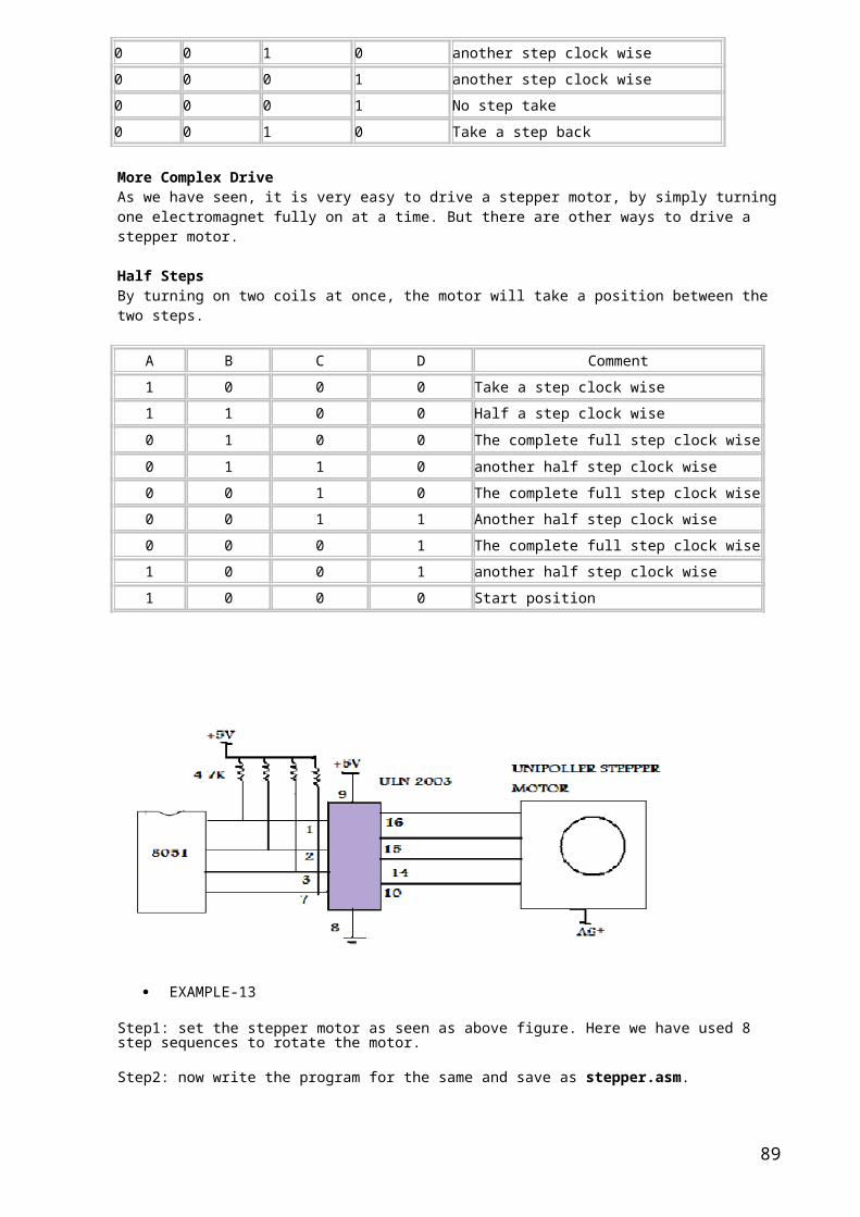
This is a sample of the large number of analog-to-digital conversion methods. The basic principle of operation is to use the comparator principle to determine whether or not to turn on a particular bit of the binary number output. It is typical for an ADC to use a digital-to-analog converter (DAC) to determine one of the inputs to the comparator.
Following are the most used converion methods:
Digital-Ramp ADC
Successive Approximation ADC
Flash ADC
►Digital-Ramp ADC
Conversion from analog to digital form inherently involves comparator action where the value of the analog voltage at some point in time is compared with some standard. A common way to do that is to apply the analog voltage to one terminal of a comparator and trigger a binary counter which drives a DAC. The output of the DAC is applied to the other terminal of the comparator. Since the output of the DAC is increasing with the counter, it will trigger the comparator at some point when its voltage exceeds the analog input. The transition of the comparator stops the binary counter, which at that point holds the digital value corresponding to the analog voltage.
►Successive Approximation ADC
Illustration of 4-bit SAC with 1 volt step size
89

The successive approximation ADC is much faster than the digital ramp ADC because it uses digital logic to converge on the value closest to the input voltage. A comparator and a DAC are used in the process. A flowchart explaining the working is shown in the figure below.
►Flash ADC
Now we lets take a look at the various Analog to Digital convectors that are most commonly used with our controllers
Name DescriptionADC0800 8-bit ADCADC0801 8-bit ADC 100us 0.25 LSBADC0802 8-bit ADC 100us 0.5 LSBADC0804 8-bit ADC 100us 1.0 LSBADC0808 8-bit 8 channel 100us ADCADC0809 8-Bit 8 channel ADC (=~ADC0808)AD571 10-Bit, A/D Converter, Complete with Reference and ClockMAX1204 5V, 8-Channel, Serial, 10-Bit ADC with 3V Digital InterfaceMAX1202 5V, 8-Channel, Serial, 12-Bit ADCs with 3V Digital InterfaceMAX195 16-Bit, Self-Calibrating, 10us Sampling ADC
90
The resistor net and comparators provide an input to the combinational logic circuit, so the conversion time is just the propagation delay through the network - it is not limited by the clock rate or some convergence sequence. It is the fastest type of ADC available, but requires a comparator for each value of output (63 for 6-bit, 255 for 8-bit, etc.) Such ADCs are available in IC form up to 8-bit and 10-bit flash ADCs (1023 comparators) are planned. The encoder logic executes a truth table to convert the ladder of inputs to the binary number output

►ADC0804 Pinout and Typical Connections
As shown in the typical circuit, ADC0804 can be interfaced with any microcontroller. You need a minimum of 11 pins to interface ADC0804, eight for data pins and 3 for control pins. As shown in the typical circuit the chip select pin can be made low if you are not using the microcontroller port for any other peripheral (multiplexing).
There is a universal rule to find out how to use an IC. All you need is the datasheet of the IC you are working with and take a look at the timing diagram of the IC which shows how to send the data, which signal to assert and at what time the signal should be made high or low etc.
Note: Keep this in mind that whenever you are working with an IC and you want to know how to communicate with that IC, and then simply look into the timing diagram of that IC from its datasheet. It gives you complete information that you need regarding the communication of IC.
91

The above timing diagrams are from ADC0804 datasheet. The first diagram (FIGURE 10A) shows how to start a conversion. Also you can see which signals are to be asserted and at what time to start a conversion. So looking into the timing diagram FIGURE 10A. We note down the steps or say the order in which signals are to be asserted to start a conversion of ADC. As we have decided to make Chip select pin as low so we need not to bother about the CS signal in the timing diagram. Below steps are for starting an ADC conversion. I am also including CS signal to give you a clear picture. While programming we will not use this signal.
Make chip select (CS) signal low.
Make write (WR) signal low.
Make chip select (CS) high.
Wait for INTR pin to go low (means conversion ends).
Once the conversion in ADC is done, the data is available in the output latch of the ADC. Looking at the FIGURE 10B which shows the timing diagram of how to read the converted value from the output latch of the ADC. Data of the new conversion is only avalable for reading after ADC0804 made INTR pin low or say when the conversion is over. Below are the stepts to read output from the ADC0804.
Make chip select (CS) pin low.
Make read (RD) signal low.
Read the data from port where ADC is connected.
92

Make read (RD) signal high.
Make chip select (CS) high.
In the next section of this tutorial we will follow the above mentioned steps to program the ADC.
EXAMPLE-19
8051 Assembly Programming for ADC0804
CODE:
rd equ P1.0 ;Read signal P1.0 wr equ P1.1 ;Write signal P1.1 cs equ P1.2 ;Chip Select P1.2 intr equ P1.3 ;INTR signal P1.3
adc_port equ P2 ;ADC data pins P2 adc_val equ 30H ;ADC read value stored here
org 0Hstart: ;Start of Program acall conv ;Start ADC conversion acall read ;Read converted value mov P3,adc_val ;Move the value to Port 3 sjmp start ;Do it again
conv: ;Start of Conversion clr cs ;Make CS low clr wr ;Make WR Low nop setb wr ;Make WR High setb cs ;Make CS highwait: jb intr,wait ;Wait for INTR signal ret ;Conversion done
read: ;Read ADC value clr cs ;Make CS Low clr rd ;Make RD Low mov a,adc_port ;Read the converted value mov adc_val,a ;Store it in local variable setb rd ;Make RD High setb cs ;Make CS High ret ;Reading done
EXAMPLE-20
►Programming 8051 in C for ADC0804
CODE:
#include <REGX51.H>#define adc_port P2 //ADC Port#define rd P1_0 //Read signal P1.0#define wr P1_1 //Write signal P1.1#define cs P1_2 //Chip Select P1.2#define intr P1_3 //INTR signal P1.3
void conv(); //Start of conversion function93

void read(); //Read ADC function
unsigned char adc_val;
void main(){ while(1){ //Forever loop conv(); //Start conversion read(); //Read ADC P3 = adc_val; //Send the read value to P3 }}
void conv(){ cs = 0; //Make CS low wr = 0; //Make WR low wr = 1; //Make WR high cs = 1; //Make CS high while(intr); //Wait for INTR to go low}
void read(){ cs = 0; //Make CS low rd = 0; //Make RD low adc_val = adc_port; //Read ADC port rd = 1; //Make RD high cs = 1; //Make CS high}
Decimal Octal Hex Binary Value ------- ----- --- ------ ----- 000 000 000 00000000 NUL (Null char.) 001 001 001 00000001 SOH (Start of Header) 002 002 002 00000010 STX (Start of Text) 003 003 003 00000011 ETX (End of Text) 004 004 004 00000100 EOT (End of Transmission) 005 005 005 00000101 ENQ (Enquiry) 006 006 006 00000110 ACK (Acknowledgment) 007 007 007 00000111 BEL (Bell) 008 010 008 00001000 BS (Backspace) 009 011 009 00001001 HT (Horizontal Tab) 010 012 00A 00001010 LF (Line Feed) 011 013 00B 00001011 VT (Vertical Tab) 012 014 00C 00001100 FF (Form Feed) 013 015 00D 00001101 CR (Carriage Return) 014 016 00E 00001110 SO (Shift Out) 015 017 00F 00001111 SI (Shift In) 016 020 010 00010000 DLE (Data Link Escape) 017 021 011 00010001 DC1 (XON) (Device Control 1) 018 022 012 00010010 DC2 (Device Control 2) 019 023 013 00010011 DC3 (XOFF)(Device Control 3)
067 103 043 01000011 C 068 104 044 01000100 D 069 105 045 01000101 E 070 106 046 01000110 F 071 107 047 01000111 G 072 110 048 01001000 H 073 111 049 01001001 I 074 112 04A 01001010 J 075 113 04B 01001011 K 076 114 04C 01001100 L 077 115 04D 01001101 M 078 116 04E 01001110 N 079 117 04F 01001111 O 080 120 050 01010000 P 081 121 051 01010001 Q 082 122 052 01010010 R 083 123 053 01010011 S 084 124 054 01010100 T 085 125 055 01010101 U 086 126 056 01010110 V 087 127 057 01010111 W 088 130 058 01011000 X 089 131 059 01011001 Y 090 132 05A 01011010 Z 091 133 05B 01011011 [ (left/opening bracket) 092 134 05C 01011100 \ (back slash)
94
020 024 014 00010100 DC4 (Device Control 4) 021 025 015 00010101 NAK (Negative Acknowledgement) 022 026 016 00010110 SYN (Synchronous Idle) 023 027 017 00010111 ETB (End of Trans. Block) 024 030 018 00011000 CAN (Cancel) 025 031 019 00011001 EM (End of Medium) 026 032 01A 00011010 SUB (Substitute) 027 033 01B 00011011 ESC (Escape) 028 034 01C 00011100 FS (File Separator) 029 035 01D 00011101 GS (Group Separator) 030 036 01E 00011110 RS (Request to Send)(Record Separator) 031 037 01F 00011111 US (Unit Separator) 032 040 020 00100000 SP (Space) 033 041 021 00100001 ! (exclamation mark) 034 042 022 00100010 " (double quote) 035 043 023 00100011 # (number sign) 036 044 024 00100100 $ (dollar sign) 037 045 025 00100101 % (percent) 038 046 026 00100110 & (ampersand) 039 047 027 00100111 ' (single quote) 040 050 028 00101000 ( (left/opening parenthesis) 041 051 029 00101001 ) (right/closing parenthesis) 042 052 02A 00101010 * (asterisk) 043 053 02B 00101011 + (plus) 044 054 02C 00101100 , (comma) 045 055 02D 00101101 - (minus or dash) 046 056 02E 00101110 . (dot) 047 057 02F 00101111 / (forward slash) 048 060 030 00110000 0 049 061 031 00110001 1 050 062 032 00110010 2 051 063 033 00110011 3 052 064 034 00110100 4 053 065 035 00110101 5 054 066 036 00110110 6 055 067 037 00110111 7 056 070 038 00111000 8 057 071 039 00111001 9 058 072 03A 00111010 : (colon) 059 073 03B 00111011 ; (semi-colon) 060 074 03C 00111100 < (less than) 061 075 03D 00111101 = (equal sign) 062 076 03E 00111110 > (greater than) 063 077 03F 00111111 ? (question mark) 064 100 040 01000000 @ (AT symbol) 065 101 041 01000001 A 066 102 042 01000010 B
093 135 05D 01011101 ] (right/closing bracket) 094 136 05E 01011110 ^ (caret/circumflex) 095 137 05F 01011111 _ (underscore) 096 140 060 01100000 ` 097 141 061 01100001 a 098 142 062 01100010 b 099 143 063 01100011 c 100 144 064 01100100 d 101 145 065 01100101 e 102 146 066 01100110 f 103 147 067 01100111 g 104 150 068 01101000 h 105 151 069 01101001 i 106 152 06A 01101010 j 107 153 06B 01101011 k 108 154 06C 01101100 l 109 155 06D 01101101 m 110 156 06E 01101110 n 111 157 06F 01101111 o 112 160 070 01110000 p 113 161 071 01110001 q 114 162 072 01110010 r 115 163 073 01110011 s 116 164 074 01110100 t 117 165 075 01110101 u 118 166 076 01110110 v 119 167 077 01110111 w 120 170 078 01111000 x 121 171 079 01111001 y 122 172 07A 01111010 z 123 173 07B 01111011 { (left/opening brace) 124 174 07C 01111100 | (vertical bar) 125 175 07D 01111101 } (right/closing brace) 126 176 07E 01111110 ~ (tilde) 127 177 07F 01111111 DEL (delete)
95