chapter 15personal.strath.ac.uk/barry.williams/book/chapter 15.pdf(15.14) if the transistor on-time...
TRANSCRIPT
Power Electronics 491
ac mains voltage feed-back for unity input power factor
15 Switched-mode
dc-to-dc Power Supplies A switched-mode power supply (smps) or switching regulator, efficiently converts a dc voltage level to another dc voltage level, via an intermediate magnetic (inductor) storage stage, such that a continuous, possibly constant, load current flows, usually at power levels below a few kilowatts.
Shunt and series linear regulator power supplies dissipate much of their energy across the regulating transistor, which operates in the linear mode. An smps achieves regulation by varying the on to off time duty cycle of the switching element. This switching minimises losses, irrespective of load conditions.
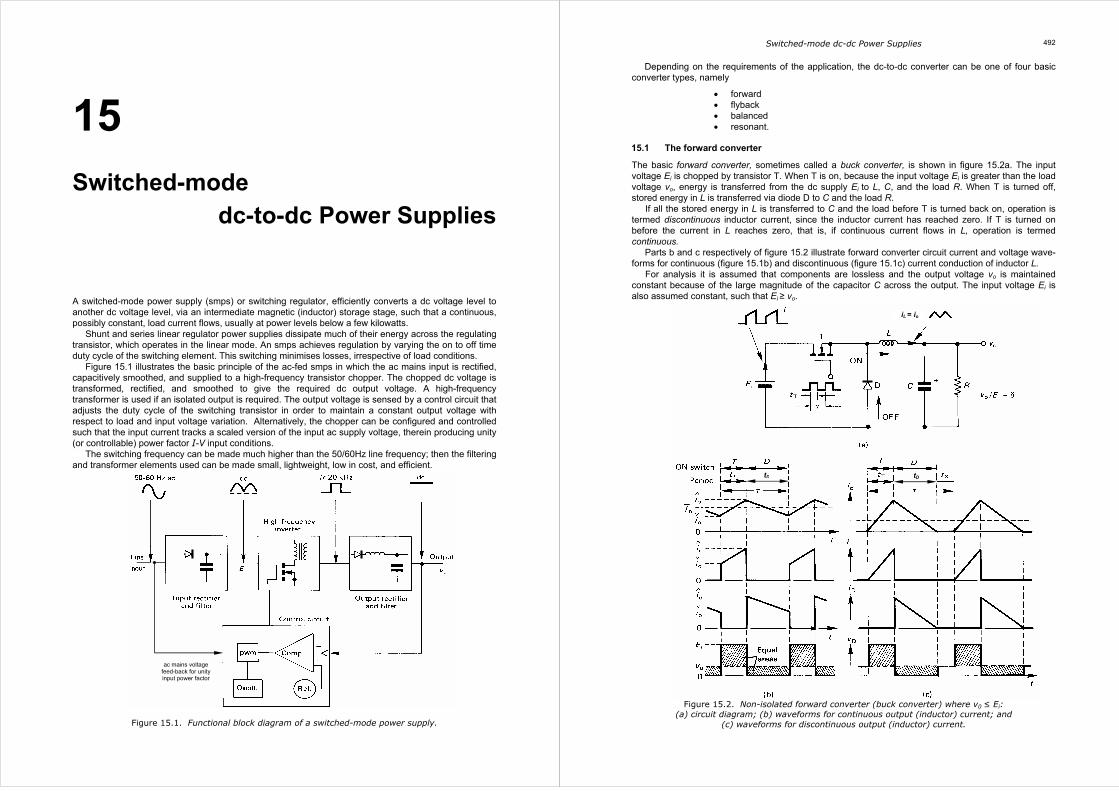
Figure 15.1 illustrates the basic principle of the ac-fed smps in which the ac mains input is rectified, capacitively smoothed, and supplied to a high-frequency transistor chopper. The chopped dc voltage is transformed, rectified, and smoothed to give the required dc output voltage. A high-frequency transformer is used if an isolated output is required. The output voltage is sensed by a control circuit that adjusts the duty cycle of the switching transistor in order to maintain a constant output voltage with respect to load and input voltage variation. Alternatively, the chopper can be configured and controlled such that the input current tracks a scaled version of the input ac supply voltage, therein producing unity (or controllable) power factor I-V input conditions.
The switching frequency can be made much higher than the 50/60Hz line frequency; then the filtering and transformer elements used can be made small, lightweight, low in cost, and efficient.
Figure 15.1. Functional block diagram of a switched-mode power supply.
Switched-mode dc-dc Power Supplies
492
Depending on the requirements of the application, the dc-to-dc converter can be one of four basic converter types, namely
• forward • flyback • balanced • resonant.
15.1 The forward converter
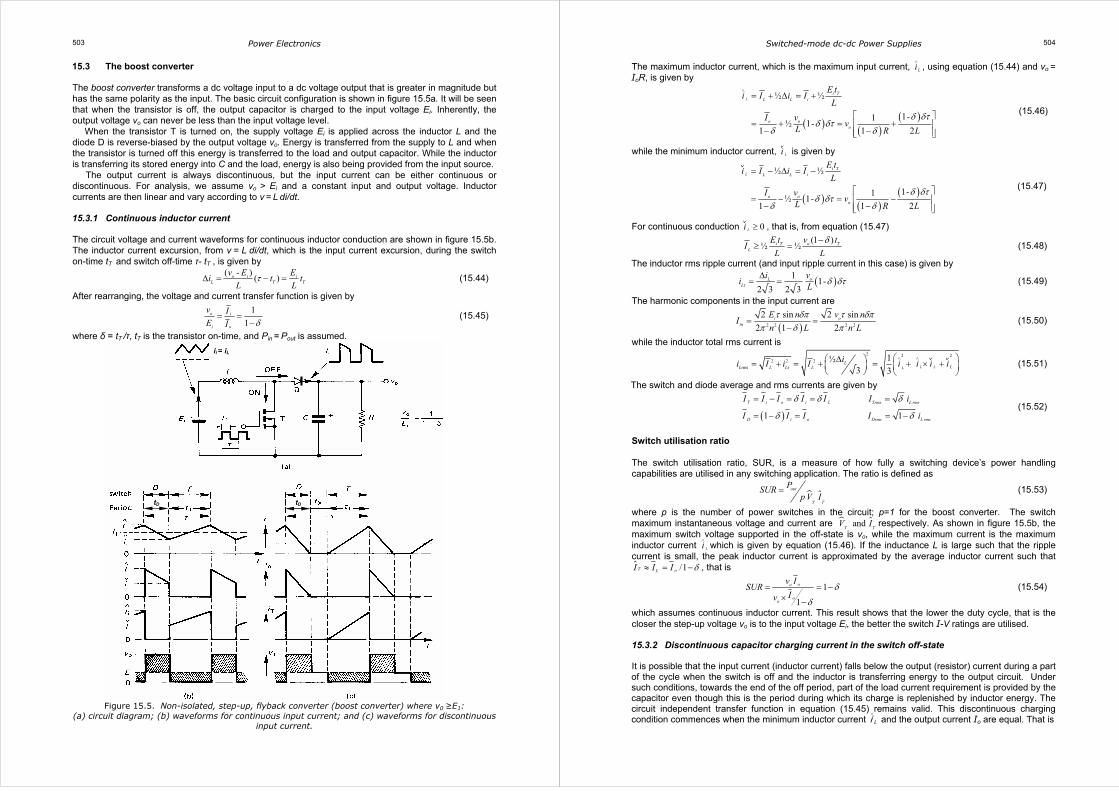
The basic forward converter, sometimes called a buck converter, is shown in figure 15.2a. The input voltage Ei is chopped by transistor T. When T is on, because the input voltage Ei is greater than the load voltage vo, energy is transferred from the dc supply Ei to L, C, and the load R. When T is turned off, stored energy in L is transferred via diode D to C and the load R.
If all the stored energy in L is transferred to C and the load before T is turned back on, operation is termed discontinuous inductor current, since the inductor current has reached zero. If T is turned on before the current in L reaches zero, that is, if continuous current flows in L, operation is termed continuous.
Parts b and c respectively of figure 15.2 illustrate forward converter circuit current and voltage wave-forms for continuous (figure 15.1b) and discontinuous (figure 15.1c) current conduction of inductor L.
For analysis it is assumed that components are lossless and the output voltage vo is maintained constant because of the large magnitude of the capacitor C across the output. The input voltage Ei is also assumed constant, such that Ei ≥ vo.
Figure 15.2. Non-isolated forward converter (buck converter) where v0 ≤ Ei: (a) circuit diagram; (b) waveforms for continuous output (inductor) current; and
(c) waveforms for discontinuous output (inductor) current.
iL = io
tD tD

Power Electronics 493
15.1.1 Continuous inductor current The inductor current is analysed first when the switch is on, then when the switch is off. When transistor T is turned on for period tT, the difference between the supply voltage Ei and the output voltage v0 is impressed across L. From V = L di/dt = L ∆i/∆t, the current change through the inductor will be
i oL LL
E vi i i t
L Τ
−∆ = − = ×
∧ ∨ (15.1)
When T is switched off for the remainder of the switching period, tD=τ- tT, the freewheel diode D conducts and -v0 is impressed across L. Thus, using V = L ∆i/∆t, rearranged, assuming continuous conduction
( )oL
vi t
L Ττ∆ = × − (15.2)
Equating equations (15.1) and (15.2) gives ( - ) ( - )i o T o TE v t v tτ= (15.3)
This expression shows that the inductor average voltage is zero, and after rearranging (Pout = Pin):
0 1o Ti
oi
v tIE I
δ δτ= = = ≤ ≤ (15.4)
This equation also shows that for a given input voltage, the output voltage is determined by the transistor conduction duty cycle δ and the output is always less than the input voltage. This confirms and validates the original analysis assumption that Ei ≥ vo. The voltage transfer function is independent of circuit inductance L and capacitance C. The inductor rms ripple current (and capacitor ripple current in this case) from equations (15.1) and (15.2), for continuous inductor current, is given by
( ) ( ). . .
r
1 11- 1-
2 3 2 3 2 3o iL
L
v Eii
L Lδ τ δ δτ
∆= = = (15.5)
while the inductor total rms current is
.
2 2 22 2 2
rms r
1½33
L LLL
LL L L L
ii I i I i i i i∧ ∧ ∆= + = + = + × +
∨ ∨ (15.6)
The switch and diode average and rms currents are given by
( )1 1
T i o Trms L rms
D o i o Drms L rms
I I I I i
I I I I I i
δ δ
δ δ
= = =
= − = − = − (15.7)
If the average inductor current, hence output current, is LI , then the maximum and minimum inductor current levels are given by
( )½ ½ 1-
1 1
2
L
oL L o
o
vi I i I
L
vR f L
δ τ
δ
∧
= + ∆ = +
−= +
(15.8)
and
( )½ ½ 1-
1 1
2
L
oL L o
o
vi I i I
L
vR f L
δ τ
δ
= − ∆ = −
−= −
∨
(15.9)
respectively, where ∆iL is given by equation (15.1) or (15.2). The average output current is ½( ) /
∧
= + = =L LL o oI i i I v R∨
. The output power is therefore 2 /ov R , which equals the input power, namely i Ti iE I E I= . Circuit waveforms for continuous inductor current conduction are shown in figure 15.2b.
Switch utilisation ratio The switch utilisation ratio, SUR, is a measure of how fully a switching device’s power handling capabilities are utilised in any switching application. The ratio is defined as
out
TT
PSURp V I
= (15.10)
where p is the number of power switches in the circuit; p=1 for the forward converter. The switch maximum instantaneous voltage and current are and
TTV I respectively. As shown in figure 15.2b, the
maximum switch voltage supported in the off-state is Ei, while the maximum current is the maximum inductor current Li
∧which is given by equation (15.8). If the inductance L is large such that the ripple
Switched-mode dc-dc Power Supplies
494
current is small, the peak inductor current is approximated by the average inductor current L oTI I I≈ = , that is
1
oo o
o ii
v I vSUR
EE Iδ= = =
× × (15.11)
which assumes continuous inductor current. This result shows that the higher the duty cycle, that is the closer the output voltage vo is to the input voltage Ei, the better the switch I-V ratings are utilised. 15.1.2 Discontinuous inductor current The onset of discontinuous inductor current operation occurs when the minimum inductor current Li
∨,
reaches zero. That is, with 0Li∨= in equation (15.9), the last equality
( )11
02R f L
δ−− = (15.12)
relates circuit component values (R and L) and operating conditions (f and δ) at the verge of discontinuous inductor current. Also, with 0Li
∨= in equation (15.9)
½L o LI I i= = ∆ (15.13)
which, after substituting equation (15.1) or equation (15.2), yields
( )
(1 )2 2
τδ τδ δ−
= = −ori o iL o
E v EI I
L L (15.14)
If the transistor on-time tT is reduced (or the load current is reduced), the discontinuous condition dead time tx is introduced as indicated in figure 15.2c. From equations (15.1) and (15.2), with 0Li
∨= , the
output voltage transfer function is now derived as follows
( )
( )i o oL T T x
E v vi t t t
L Lτ−
= = − −∧
(15.15)
that is
0 1 01
δ δ
τ
= ≤ < ≥−
andox
xi
vt
tE (15.16)
This voltage transfer function form may not be particularly useful since the dead time tx is not expressed in term of circuit parameters. Accordingly, from equation (15.15)
( )i o
L T
E vi t
L
−=
∧ (15.17)
and from the input current waveform in figure 15.2c:
½ TLi
tI i τ= ×
∧ (15.18)
Eliminating Li∧
yields
2
(1 )i o i
i
I v E
E L
τδδ
= − (15.19)
that is
2
21o i
i i
v LIE Eδ τ
= − (15.20)
Assuming power-in equals power-out, that is, i i o o o LE I v I v I= = , the input average current can be eliminated, and after re-arranging yields:
2 2
1 1
2 21 1δ τ δ τ
= =+ +
o
i o i
i o
v
E LI LI
E v
(15.21)
At a low output current or high input voltage, there is a likelihood of discontinuous inductor conduction. To avoid discontinuous conduction, larger inductance values are needed, which worsen transient response. Alternatively, with extremely low on-state duty cycles, a voltage-matching transformer can be used to increase δ. Once a transformer is used, any smps technique can be used to achieve the desired output voltage. Figures 15.2b and c show that the input current is always discontinuous.

Power Electronics 495
15.1.3 Load conditions for discontinuous inductor current As the load current decreases, the inductor average current also decreases, but the inductor ripple current magnitude is unchanged. If the load resistance is increased sufficiently, the bottom of the triangular inductor current, Li
∨, eventual reduces to zero. Any further increase in load resistance causes
discontinuous inductor current and the linear voltage transfer function given by equation (15.4) is no longer valid and equations (15.16) and (15.20) are applicable. The critical load resistance for continuous inductor current is specified by
½
o ocrit
Lo
v vR
iI≤ =
∆ (15.22)
Substitution for vo from equation (15.2) and using the fact that o LI I= , yields
( )
o Lcrit
o L
v i LR
I I tΤτ∆
≤ =−
(15.23)
Eliminating Li∆ by substituting the limiting condition given by equation (15.13) gives
2 2
( ) ( ) ( )o L L
crit
o L L
v i L I L LR
I I t I t tΤ Τ Ττ τ τ∆
≤ = = =− − −
(15.24)
Dividing throughout by τ and substituting /Ttδ τ= yields
2 2
( ) (1 )o
crit
o
v L LR
I tΤτ τ δ≤ = =
− − (15.25)
The critical resistance can be expressed in a number of forms. By substituting the switching frequency ( 1/sf τ= ) or the fundamental inductor reactance ( 2L sX f Lπ= ) the following forms result.
22 2
( )(1 ) (1 ) (1 ) (1 )τ δ τδ δ δ π δ
≤ = = × = = Ω− − − −
o o s Lcrit
io
v v f L XL LR
EI (15.26)
Notice that equation (15.26) is in fact equation (15.12), re-arranged. If the load resistance increases beyond Rcrit, the output voltage can no longer be maintained with duty cycle control according to the voltage transfer function in equation (15.4). 15.1.4 Control methods for discontinuous inductor current Once the load current has reduced to the critical level as specified by equation (15.26), the input energy is in excess of the load requirement. Open loop load voltage regulation control is lost and the capacitor C tends to overcharge. Hardware approaches can be used to solve this problem – by producing continuous inductor current
• increase L thereby decreasing the inductor current ripple peak-to-peak magnitude • step-down transformer impedance matching to effectively reduce the apparent load impedance
Two control approaches to maintain output voltage regulation when R > Rcrit are
• vary the switching frequency fs, maintaining the switch on-time tT constant so that ∆iL is fixed or • reduce the switch on-time tT , but maintain a constant switching frequency fs, thereby reducing ∆iL.
If a fixed switching frequency is desired for all modes of operation, then reduced on-time control, using output voltage feedback, is preferred. If a fixed on-time mode of control is used, then the output voltage is control by varying inversely the frequency with output voltage. 15.1.4i - fixed on-time tT, variable switching frequency fvar The operating frequency fvar is varied while the switch-on time tT is maintained constant such that the ripple current remains unchanged. Operation is specified by equating the input energy and the output energy, thus maintaining a constant capacitor charge, hence output voltage. That is, equating energies
2
var
1½ o
L i T
vi E t
R f∆ = (15.27)
Isolating the variable switching frequency fvar gives
2
var
1
½o
L i T
vf
i E t R=
∆
var
var
1
1
s critf f RR
fR
α
= × (15.28)
Switched-mode dc-dc Power Supplies
496
That is, once discontinuous inductor current occurs, if the switching frequency is varied inversely with load resistance and the switch on-state period is maintained constant, output voltage regulation can be maintained. Load resistance R is not a directly or readily measurable parameter for feedback proposes. Alternatively, since o ov I R= substitution for R in equation (15.28) gives
var
var
crits o
o
o
Rf f I
v
f Iα
= × (15.29)
That is, for /< ∆ <oro L o o critI i I v R½ , if tT remains constant and fvar is varied proportionally with load current, then the required output voltage vo will be maintained. 15.1.4ii - fixed switching frequency fs, variable on-time tTvar The operating frequency fs remains fixed while the switch-on time tTvar is reduced, resulting in the ripple current being reduced. Operation is specified by equating the input energy and the output energy as in equation (15.27), thus maintaining a constant capacitor charge, hence voltage. That is
2
var
1½ o
L i T
s
vi E t
R f∆ = (15.30)
Isolating the variable on-time tTvar yields
2
var
1
½o
T
L i s
vt
i E f R=
∆
Substituting ∆iL from equation (15.2) gives
.
.
var
var
1
1
T T crit
T
t t RR
tR
α
= × (15.31)
That is, once discontinuous inductor current commences, if the switch on-time is varied inversely to the square root of the load resistance, maintaining the switching frequency constant, regulation of the output voltage can be maintained. Again, load resistance R is not a directly or readily measurable parameter for feedback proposes and substitution of /o ov I for R in equation (15.31) gives
.
.
var
var α
= ×critT T o
o
T o
Rt t I
v
t I
(15.32)
That is, if fs is fixed and tT is reduced proportionally to . oI , when o LI i< ∆½ /<or o o critI v R , then the required output voltage magnitude vo will be maintained. 15.1.5 Output ripple voltage Three components contribute to the output voltage ripple
• Ripple charging/discharging of the ideal output capacitor, C • Capacitor equivalent series resistance, ESR • Capacitor equivalent series inductance, ESL
The capacitor inductance and resistance parasitic series component values decrease as the quality of the capacitor increases. The output ripple voltage is the vectorial summation of the three components that are shown in figure 15.3 for the forward converter. Ideal Capacitor: The ripple voltage for a capacitor is defined as
1C Cv i dt∆ = ∫
Figures 15.2 and 15.3 show that for continuous inductor current, the inductor current which is the output current, swings by ∆i around the average output current, oI , thus
1 12 2½C C Civ i dt τ∆∆ = =∫ (15.33)
Substituting for Li∆ from equation (15.2)
18
1 1 12 2
½ ( )τ τ τΤ∆∆ = = = × −∫C C C
oiC
vL
v i dt t (15.34)

Power Electronics 497
If ESR and ESL are ignored, after rearranging, equation (15.34) gives the percentage voltage ripple (peak to peak) in the output voltage
½
2 218
1 (1 ) ½ (1 )C o c
so oLC
v v ffv v
δ τ π δ∆ ∆ = = × − = −
(15.35)
In complying with output voltage ripple requirements, from this equation, the switching frequency fs=1/τ must be much higher that the cut-off frequency given by the forward converter low-pass, second-order LC output filter, fc = 1/2π√LC. The voltage switching harmonics before filtering are the dc part δEi and
2
1 cos 2π δπ
= −in
EV n
n (15.36)
ESR: The equivalent series resistor voltage follows the ripple current, that is, it swings linearly about ½ESR ESRV i R= ± ∆ × (15.37)
ESL: The equivalent series inductor voltage is derived from / ,=v Ldi dt that is, when the switch is on
/ /ESL onV L i t L i δτ+ = ∆ = ∆ (15.38)
When the switch is off ( )/ / 1
ESL offV L i t L i δ τ− = − ∆ = − ∆ − (15.39)
The total instantaneous ripple voltage is o C ESR ESLv v V V∆ = ∆ + + (15.40)
Forming a time domain solution for each component, then differentiating, gives a maximum ripple when 2 (1 )ESRt CR δ= − (15.41)
This expression is independent of the equivalent series inductance, which is expected since it is constant during each operational state. If dominant, the inductor will affect the output voltage ripple at the switch turn-on and turn-off instants.
Figure 15.3. Forward converter, three output ripple components, showing: left - voltage components; centre – waveforms; and right - capacitor model.
Example 15.1: Buck (step-down forward) converter The step-down converter in figure 15.2a operates at a switching frequency of 10 kHz. The output voltage is to be fixed at 48 V dc across a 1 Ω resistive load. If the input voltage Ei =192 V and the choke L = 200µH:
i. calculate the switch T on-time duty cycle δ and switch on-time tT. ii. calculate the average load current oI , hence average input current iI . iii. draw accurate waveforms for
• the voltage across, and the current through L; vL and iL • the capacitor current, ic • the switch and diode voltage and current; vT, vD, iT, iD.
iC
VC
VESR VESL
∆i
τ∆i/8C
∆i R
L∆i/ton
L∆i/tD
o
o o o
vc = vo
-
Switched-mode dc-dc Power Supplies
498
Hence calculate the switch utilisation ratio as defined by equation (15.11). iv. calculate the mean and rms current ratings of diode D, switch T and L. v. calculate the capacitor average and rms current, iCrms and output ripple voltage if the capacitor
has an internal equivalent series resistance of 20mΩ, assuming C = ∞. vi. calculate the maximum load resistance Rcrit before discontinuous inductor current. Calculate the
output voltage and inductor non-conduction period, tx, when the load resistance is triple the critical resistance Rcrit.
vii. if the maximum load resistance is 1Ω, calculate • the value the inductance L can be reduced, to be on the verge of discontinuous inductor
current and for that L • the peak-to-peak ripple and rms, inductor and capacitor currents.
viii. specify two control strategies for controlling the forward converter in a discontinuous inductor current mode.
ix. output ripple voltage hence percentage output ripple voltage, for C = 1,000µF and an equivalent series inductance of ESL = 0.5µH, assuming ESR = 0Ω.
Solution i. From equation (15.4), assuming continuous inductor current, the duty cycle δ is
48V
= ¼ = 25%192V
o
i
v
Eδ = =
Also, from equation (15.4), for a 10kHz switching frequency, the switching period τ is 100µs and the transistor on-time tT is given by
48V
192V 100µso T T
i
v t t
E τ= = =
whence the transistor on-time is 25µs and the diode conducts for 75µs.
ii. The average load current is 48V
= 48A =1Ω
oo L
vI I
R= =
From power-in equals power-out, the average input current is / 48V×48A/192V = 12Ai o o iI v I E= =
iii. From equation (15.1) (or equation (15.2)) the inductor peak-to-peak ripple current is
192V-48V
×25µs = 18A200µH
i oL
E vi t
L Τ
−∆ = × =
From part ii, the average inductor current is the average output current, 48A. The inductor current is continuous since 39 .L Ai
∨= Circuit voltage and current waveforms are shown in the following figure.
The circuit waveforms show that the maximum switch voltage and current are 192V and 57A respectively. The switch utilising ratio is given by equation (15.11), that is
2248V1 21%
192V 57A
o
out
o oi i
vP RSUR
E i E iΩ= = = ≡
×× ×
If the ripple current were assume small, the resulting SUR value of δ = 33% gives a misleading under-estimate indication. iv. Current iD through diode D is shown on the inductor current waveform. The average diode current is
(1 ) (1 ¼)×48A = 36ATD L L
tI I I
τ δτ−
= × = − × = −
The rms diode current is given by
. .
75µs2 2
rms 0 0
1 1 18A( ) (57A ) = 41.8A
100µs 75µs-
TtL
LDT
ii i t dt t dtt
τ
ττ− ∧ ∆
= − =−∫ ∫
Current iT through the switch T is shown on the inductor current waveform. The average switch current is
¼×48A = 12ATT L L
tI I Iδτ= = =
Alternatively, from power-in equals power-out / 48V×48A/192V = 12AT i o o iI I v I E= = =

Power Electronics 499
The transistor rms current is given by
. .
25µs2 2
rms 0 0
1 1 18A( ) (39A+ )
100µs 25µs
= 24.1A
T
L
tL
TT
ii i t dt t dt
tτ∆
= + =∫ ∫∨
The mean inductor current is the mean output current, 48A= =o LI I .
The inductor rms current is given by equation (15.6), that is
2 2
2 2½ ½ 18A48A 48.3A3 3
LL rms L
iI I ∆ ×= + = + =
v. The average capacitor current CI is zero and the rms ripple current is given by
.
.
2 21 1
2 2rms 0 0
25µs 75µs2 2
0 0
1( ) ( )
1 18A 18A(-9A+ ) (9A- )
100µs 25µs 75µs
= 5.2A (= / 2 3)
T Tt tL L
C L LT T
L
i ii i t dt i t dt
t t
t dt t dt
i
τ
τ τ− ∆ ∆
= − ∆ + + ∆ − −
= +
∆
∫ ∫
∫ ∫
The capacitor voltage ripple (hence the output voltage ripple), assuming infinite output capacitance, is determined by the capacitor ripple current which is equal to the inductor ripple current, 18A p-p, that is
ripple esr
= 18A×20mΩ = 360mV
= ∆ ×
p -po L Cv i R
and the rms output voltage ripple is
rms rms esr
= 5.2A ×20mΩ = 104mV
= ×rms rms
o C Cv i R
vi. Critical load resistance is given by equation (15.26), namely
2
(1 )o
crit
o
v LR
I τ δ≤ =
−
Figure: Example 15.1
192V
(V)
0 25
Icap VDiode
VTran VDiode
VTran
18A
Ei -vo
125
3.6mV.s
Switched-mode dc-dc Power Supplies
500
1
3
2×200µH= 16/3
100µs (1-¼)
= 5 Ω =9AoI
= Ω×
when
Alternatively, the critical load current is 9A (½ ∆iL), thus from the equation immediately above, the load resistance must not be greater than /o ov I = 48V/9A = 5⅓Ω, if the inductor current is to be continuous. When the load resistance is tripled to 16Ω the output voltage is given by equation (15.20), which is shown normalised in table 15.2. That is
2
2
2
2
8 16 100µs¼ 1 1 8
200µH
8192V ¼ 8 ¼ 1 1 75V 14.625A
¼ 8
τδδ
Ω×= × − + + = = =
= × × × × − + + = = ×
where thuso i
Lo
Rv E k k
k L
v i
The inductor current is zero for an interval of the 100µs switching period, and the time is given by the appropriate normalised expression involving tx for the forward converter in table 15.2 or by equation (15.16), which when re-arranged to isolate tx becomes
[ ]T D1 100µs 1 36µs = 25µs =39µs75V
50V
¼δτ
= − = × − =
xo
i
t t tv
E
vii. The critical resistance formula given in equation (15.26) is valid for finding critical inductance when inductance is made the subject of the equation, that is, rearranging equation (15.26) gives
= ½ (1 ) (H)
= ½×1Ω×(1-¼)×100µs = 37½µHcritL R δ τ× × − ×
This means the inductance can be reduced from 200µH with a 48A mean and 18A p-p ripple current, to 37½µH with the same 48A mean plus a superimposed 96A p-p ( )2 LI ripple current. The rms capacitor current is given by
.
.
rms = / 2 3
= 96A/2 3 = 27.2A
∆
rms
C Li i
The inductor rms current requires the following integration
.
.
2 2
rms 0 0
25µs 75µs2 2
0 0
1( ) ( )
1 96A 96A(0 + ) (96A - )
100µs 25µs 75µs
= 96/ 3 = 55.4 A
τ
τ τ− ∧ ∆ ∆
= + + − −
= × +
∫ ∫
∫ ∫rms
T T
L
t tL L
LLT T
i ii i t dt i t dt
t t
t dt t dt
∨
or from equation (15.6)
2 2
ripplerms
2 248 (96 / 2 3) = 55.4 A
= +
= + rms
LL Lii I
viii. For R >16/3Ω, or 9AoI < , equations (15.29) or (15.32) can be used to develop a suitable control strategy.
(a) From equation (15.29), using a variable switching frequency of less than 10kHz,
13
var
var
5 Ω10kHz
48V
10kHz
9
crits o o
o
o
Rf f I Iv
f I
= =
= ×
(b) From equation (15.32), maintaining a fixed switching frequency of 10kHz, the on-time duty cycle is reduced (from 25µs) for 9AoI < according to
. .
.
13
var
var
5 Ω25µs
48V
25µs
3
= =
= ×
critT T o o
o
T o
Rt t I Iv
t I

Power Electronics 501
ix. From equation (15.33) the output ripple voltage with an ideal 1,000µF capacitor is given by
8
18A 100µs= 225mV
8 1000µF
τ∆∆
×=
×
=
p -p
C
iv
C
The voltage produced because of the equivalent series 0.5 µH inductance is
( )
/
=0.5µH×18A/0.25×100µs = 360mV
/ 1
= - 0.5µH×18A/(1 - 0.25)×100µs = -120mV
ESL
ESL
V L i
V L i
δτ
δ τ
+
−
= ∆
= − ∆ −
Time domain summation of the capacitor and ESL inductor voltages show that the peak to peak output voltage swing is determined by the ESL inductor, giving
= 360mV + 120mV = 480mVo ESL ESLv V V+ −∆ = −
The percentage ripple in the output voltage is 480mV/48V = 1%. ♣
15.1.6 Underlying operational mechanisms of the forward converter The inductor current is pivotal to the analysis and understanding of any smps. For analysis, the smps internal and external electrical conditions are in steady-state on a cycle-by-cycle basis and the input power is equal to the output power. The first concept to appreciate is that the net capacitor charge change is zero over each switching cycle. That is, the average capacitor current is zero:
( )
10
t
c ct
I i t dtτ
τ+
= =∫
In so being, the output capacitor provides any load current deficit and stores any load current (inductor) surplus associated with the inductor current within each complete cycle. Thus, the capacitor is a temporary storage component where the capacitor voltage is fixed on a cycle-by-cycle basis, and because of its large capacitance does not vary significantly within a cycle. The second concept involved is that the average inductor voltage is zero. Based on / ,=v L di dt the equal area criteria in chapter 11.1.1i,
( )
10
t
t t L t tt
i i v t dt i iL
τ
τ τ
+
+ +− = = =∫ since in steady - state
Thus the average inductor voltage is zero:
( )
10
t
LLt
V v t dtτ
τ+
= =∫
The most enlightening way to appreciate the converter operating mechanisms is to consider how the inductor current varies with load resistance R and inductance L. The figure 15.4 shows the inductor current associated with the various parts of example 15.1.
For continuous inductor current operation, the two necessary and sufficient equations are Io = vo /R and equation (15.2). Since the duty cycle and on-time are fixed for a given output voltage requirement, equation (15.2) can be simplified to show that the ripple current is inversely proportional to inductance, as follows
( )
1
oL
L
vi t
L
iL
Ττ
α
∆ = × −
∆ (15.42)
Since the average inductor current is equal to the load current, then, at a given output voltage, the average inductor current is inversely proportional to the load resistance, that is
/
1L o o
L
I I v R
IR
α
= = (15.43)
Switched-mode dc-dc Power Supplies
502
Figure 15.4. Forward converter (buck converter) operational mechanisms showing that: (a) the average inductor current is inversely proportional to load resistance R (fixed L) and (b) the
inductor ripple current magnitude is inversely proportional to inductance L (fixed load R). Equation (15.43) predicts that the average inductor current is inversely proportional to the load resistance, as shown in figure 15.4a. As the load is increased (load resistor decreased), the triangular inductor current moves vertically up, but importantly, from equation (15.42), the peak-to-peak ripple current is constant, that is the ripple current is independent of the load. As the load current is progressively decreased, by increasing R, the peak-to-peak current is unchanged; the inductor minimum current eventually reduces to zero, and discontinuous inductor current operation occurs. Equation (15.42) indicates that the inductor ripple current is inversely proportional to inductance, as shown in figure 15.4b. As the inductance is varied the ripple current varies inversely, but importantly, from equation (15.43), the average current is constant, and specifically the average current value is not related to inductance L and is solely determined by the load current, vo /R. As the inductance decreases the magnitude of the ripple current increases, the average is unchanged, and the minimum inductor current eventually reaches zero and discontinuous inductor current operation results. 15.2 Flyback converters
Flyback converters store energy in an inductor, (‘choke’), before transferring any energy to the load/load storage capacitor such that controllable output voltage magnitudes in excess of the input voltage are attainable. The key characteristic is that whilst energy is being transferred to the inductor, all the load energy is provided by the output capacitor. Such converters are also known as ringing choke converters. Two basic (minimum component count and transformerless) versions of the flyback converter are possible, both are integral to the same underlying fundamental circuit configuration.
• The step-up voltage flyback converter, called the boost converter, where the input and output voltage have the same polarity - non-inversion, and vo ≥ Ei.
• The step-up/step-down voltage flyback converter, called the buck-boost converter, where output voltage polarity inversion occurs, that is vo ≥ 0.
decr
easi
ngL
dec
reas
ing
RLO
AD
LI IL Rload L IL ILp-p
0 25µs 100µs t 0 25µs 100µs t (a) (b)
Ω
1Ω 2Ω 16/3Ω
96A 36A 18A
200µH
100µH
37½µH
72A
48A
24A
9A
verge of discontinuous
inductor current
δ δ 1-δ 1-δ
vo/R
vo/R
Power Electronics 503
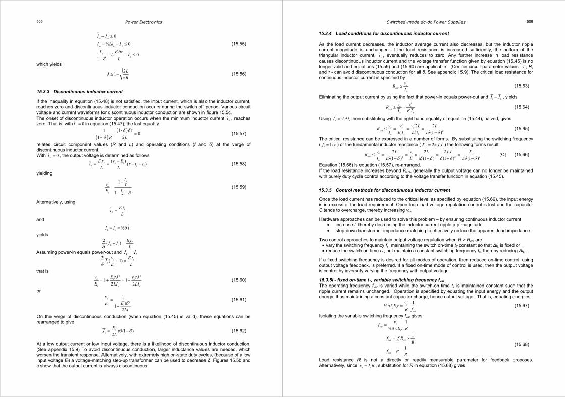
15.3 The boost converter The boost converter transforms a dc voltage input to a dc voltage output that is greater in magnitude but has the same polarity as the input. The basic circuit configuration is shown in figure 15.5a. It will be seen that when the transistor is off, the output capacitor is charged to the input voltage Ei. Inherently, the output voltage vo can never be less than the input voltage level.
When the transistor T is turned on, the supply voltage Ei is applied across the inductor L and the diode D is reverse-biased by the output voltage vo. Energy is transferred from the supply to L and when the transistor is turned off this energy is transferred to the load and output capacitor. While the inductor is transferring its stored energy into C and the load, energy is also being provided from the input source.
The output current is always discontinuous, but the input current can be either continuous or discontinuous. For analysis, we assume vo > Ei and a constant input and output voltage. Inductor currents are then linear and vary according to v = L di/dt. 15.3.1 Continuous inductor current The circuit voltage and current waveforms for continuous inductor conduction are shown in figure 15.5b. The inductor current excursion, from v = L di/dt, which is the input current excursion, during the switch on-time tT and switch off-time τ- tT , is given by
( - )
( )o i iL T T
v E Ei t t
L Lτ∆ = − = (15.44)
After rearranging, the voltage and current transfer function is given by
1
1o i
oi
v IE I δ
= =−
(15.45)
where δ = tT /τ, tT is the transistor on-time, and Pin = Pout is assumed.
Figure 15.5. Non-isolated, step-up, flyback converter (boost converter) where v0 ≥E1:
(a) circuit diagram; (b) waveforms for continuous input current; and (c) waveforms for discontinuous input current.
ii = iL
tD tD
Switched-mode dc-dc Power Supplies
504
The maximum inductor current, which is the maximum input current, ∧
Li , using equation (15.44) and vo =
IoR, is given by
( ) ( )( )
½ ½
1-1½ 1-
1 1 2
L
i TL L i
o oo
E ti I i I
L
I vv
L R L
δ δτδ δτ
δ δ
∧
= + ∆ = +
= + = +
− −
(15.46)
while the minimum inductor current, Li∨
is given by
( ) ( )
( )
½ ½
1-1½ 1-
1 1 2
δ δτδ δτ
δ δ
= − ∆ = −
= − = −
− −
L
i TL L i
o oo
E ti I i I
L
I vv
L R L
∨
(15.47)
For continuous conduction 0Li ≥∨
, that is, from equation (15.47)
(1 )
½ ½δ−
≥ =i T o TL
E t v tI
L L (15.48)
The inductor rms ripple current (and input ripple current in this case) is given by
( ). .
r
11-
2 3 2 3oL
L
vii
Lδ δτ
∆= = (15.49)
The harmonic components in the input current are
( )2 2 2 2
2 sin 2 sin
2 1 2i o
in
E n v nI
n L n L
τ δπ τ δππ δ π
= =−
(15.50)
while the inductor total rms current is
.
2 2 22 2 2
rms r
1½3 3
L LLL
LL L L L
ii I i I i i i i∧ ∧ ∆= + = + = + × +
∨ ∨ (15.51)
The switch and diode average and rms currents are given by
( )1 1
T i o i L Trms L rms
D i o Drms L rms
I I I I I I i
I I I I i
δ δ δ
δ δ
= − = = =
= − = = − (15.52)
Switch utilisation ratio The switch utilisation ratio, SUR, is a measure of how fully a switching device’s power handling capabilities are utilised in any switching application. The ratio is defined as
out
TT
PSURp V I
= (15.53)
where p is the number of power switches in the circuit; p=1 for the boost converter. The switch maximum instantaneous voltage and current are and
TTV I respectively. As shown in figure 15.5b, the
maximum switch voltage supported in the off-state is vo, while the maximum current is the maximum inductor current Li
∧which is given by equation (15.46). If the inductance L is large such that the ripple
current is small, the peak inductor current is approximated by the average inductor current such that /1T oLI I I δ≈ = − , that is
1
1
oo
oo
v ISUR
Ivδ
δ
= = −× −
(15.54)
which assumes continuous inductor current. This result shows that the lower the duty cycle, that is the closer the step-up voltage vo is to the input voltage Ei, the better the switch I-V ratings are utilised. 15.3.2 Discontinuous capacitor charging current in the switch off-state It is possible that the input current (inductor current) falls below the output (resistor) current during a part of the cycle when the switch is off and the inductor is transferring energy to the output circuit. Under such conditions, towards the end of the off period, part of the load current requirement is provided by the capacitor even though this is the period during which its charge is replenished by inductor energy. The circuit independent transfer function in equation (15.45) remains valid. This discontinuous charging condition commences when the minimum inductor current Li
∨ and the output current Io are equal. That is
Power Electronics 505
0
½ 0
½ 01
oL
oLL
ioo
I I
I i I
EII
L
δτδ
∨
− ≤
− ∆ − ≤
− − ≤−
(15.55)
which yields
2
1L
Rδ
τ≤ − (15.56)
15.3.3 Discontinuous inductor current
If the inequality in equation (15.48) is not satisfied, the input current, which is also the inductor current, reaches zero and discontinuous inductor conduction occurs during the switch off period. Various circuit voltage and current waveforms for discontinuous inductor conduction are shown in figure 15.5c. The onset of discontinuous inductor operation occurs when the minimum inductor current Li
∨, reaches
zero. That is, with 0Li∨= in equation (15.47), the last equality
( )
( )1-10
1 2R L
δ δτδ
− =−
(15.57)
relates circuit component values (R and L) and operating conditions (f and δ) at the verge of discontinuous inductor current. With 0Li =
∨, the output voltage is determined as follows
( )
( )Li T o i
T x
E t v Ei t t
L Lτ
∧ −= = − − (15.58)
yielding
1
1
x
o
xi
tv
tE
τ
δτ
−=
− − (15.59)
Alternatively, using
Li TE t
iL
∧=
and
½ LL oI I iδ∧
− =
yields
2
( ) i TL o
E tI I
Lδ− =
Assuming power-in equals power-out and L iI I=
2
( 1)o i To
i
v E tI
E Lδ− =
that is
2 2
1 12 2
τδ τδ= + = +o i o
i o i
v E v
E LI LI (15.60)
or
2
1
12
τδ=
−
o
ii
i
v
EELI
(15.61)
On the verge of discontinuous conduction (when equation (15.45) is valid), these equations can be rearranged to give
(1 )2
io
EI
Lτδ δ= − (15.62)
At a low output current or low input voltage, there is a likelihood of discontinuous inductor conduction. (See appendix 15.9) To avoid discontinuous conduction, larger inductance values are needed, which worsen the transient response. Alternatively, with extremely high on-state duty cycles, (because of a low input voltage Ei) a voltage-matching step-up transformer can be used to decrease δ. Figures 15.5b and c show that the output current is always discontinuous.
Switched-mode dc-dc Power Supplies
506
15.3.4 Load conditions for discontinuous inductor current As the load current decreases, the inductor average current also decreases, but the inductor ripple current magnitude is unchanged. If the load resistance is increased sufficiently, the bottom of the triangular inductor current, Li
∨, eventually reduces to zero. Any further increase in load resistance
causes discontinuous inductor current and the voltage transfer function given by equation (15.45) is no longer valid and equations (15.59) and (15.60) are applicable. (Certain circuit parameter values - L, R, and τ - can avoid discontinuous conduction for all δ. See appendix 15.9). The critical load resistance for continuous inductor current is specified by
ocrit
o
vR
I≤ (15.63)
Eliminating the output current by using the fact that power-in equals power-out and i LI I= , yields
2
o ocrit
o i L
v vR
I E I≤ = (15.64)
Using ½L LI i= ∆ then substituting with the right hand equality of equation (15.44), halved, gives
2 2
2 2
2 2
(1 )o o o
crit
o i L i T
v v v L LR
I E I E t τδ δ≤ = = =
− (15.65)
The critical resistance can be expressed in a number of forms. By substituting the switching frequency ( 1/sf τ= ) or the fundamental inductor reactance ( 2L sX f Lπ= ) the following forms result.
2 2 2
22 2( )
(1 ) (1 ) (1 ) (1 )τδ δ τδ δ δ δ πδ δ≤ = = × = = Ω
− − − −o o s L
crit
io
v v f L XL LR
EI (15.66)
Equation (15.66) is equation (15.57), re-arranged. If the load resistance increases beyond Rcrit, generally the output voltage can no longer be maintained with purely duty cycle control according to the voltage transfer function in equation (15.45).
15.3.5 Control methods for discontinuous inductor current Once the load current has reduced to the critical level as specified by equation (15.66), the input energy is in excess of the load requirement. Open loop load voltage regulation control is lost and the capacitor C tends to overcharge, thereby increasing vo.
Hardware approaches can be used to solve this problem – by ensuring continuous inductor current • increase L thereby decreasing the inductor current ripple p-p magnitude • step-down transformer impedance matching to effectively reduce the apparent load impedance
Two control approaches to maintain output voltage regulation when R > Rcrit are • vary the switching frequency fs, maintaining the switch on-time tT constant so that ∆iL is fixed or • reduce the switch on-time tT , but maintain a constant switching frequency fs, thereby reducing ∆iL.
If a fixed switching frequency is desired for all modes of operation, then reduced on-time control, using output voltage feedback, is preferred. If a fixed on-time mode of control is used, then the output voltage is control by inversely varying the frequency with output voltage.
15.3.5i - fixed on-time tT, variable switching frequency fvar The operating frequency fvar is varied while the switch-on time tT is maintained constant such that the ripple current remains unchanged. Operation is specified by equating the input energy and the output energy, thus maintaining a constant capacitor charge, hence output voltage. That is, equating energies
2
var
1½ o
L i
vi E
R fτ∆ = (15.67)
Isolating the variable switching frequency fvar gives
2
var
1
½o
L i
vf
i E Rτ=
∆
var
var
1
1
s critf f RR
fR
α
= × (15.68)
Load resistance R is not a directly or readily measurable parameter for feedback proposes. Alternatively, since o ov I R= , substitution for R in equation (15.68) gives

Power Electronics 507
var
var
crits o
o
o
Rf f I
v
f Iα
= × (15.69)
That is, for discontinuous inductor current, namely /< ∆ <ori L o o critI i I v R½ , if the switch on-state period tT remains constant and fvar is either varied proportionally with load current or varied inversely with load resistance, then the required output voltage vo will be maintained. 15.3.5ii - fixed switching frequency fs, variable on-time tTvar The operating frequency fs remains fixed while the switch-on time tTvar is reduced such that the ripple current can be reduced. Operation is specified by equating the input energy and the output energy as in equation (15.67), thus maintaining a constant capacitor charge, hence voltage. That is
2
var
1½ o
L i T
s
vi E t
R f∆ = (15.70)
Isolating the variable on-time tTvar gives
2
var
1
½o
T
L i s
vt
i E f R=
∆
Substituting ∆iL from equation (15.44) gives
.
.
var
var
1
1
T T crit
T
t t RR
tR
α
= × (15.71)
Again, load resistance R is not a directly or readily measurable parameter for feedback proposes and substitution of /o ov I for R in equation (15.71) gives
.
.
var
var α
= ×critT T o
o
T o
Rt t I
v
t I
(15.72)
That is, if the switching frequency fs is fixed and switch on-time tT is reduced proportionally to . oI or inversely to . R , when discontinuous inductor current commences, namely /< ∆ <ori L o o critI i I v R½ , then the required output voltage magnitude vo will be maintained. 15.3.6 Output ripple voltage The output ripple voltage is the capacitor ripple voltage. The ripple voltage for a capacitor is defined as
1o Cv i dt∆ = ∫
Figure 15.5 shows that for continuous inductor current, the constant output current oI is provided solely from the capacitor during the period tT when the switch is on, thus
1 1∆ = =∫ oo TC Cv i dt t I
Substituting for /o oI v R= gives
1 1 1∆ = = =∫ ooo T TC C C
vv i dt t tI R
Rearranging gives the percentage voltage ripple (peak to peak) in the output voltage
o
o
v
v R C
δ τ∆= (15.73)
The capacitor equivalent series resistance and inductance can be account for, as with the forward converter, 15.1.4. When the switch conducts, the output current is constant and is provided from the capacitor. Thus no ESL voltage effects result during this constant capacitor current portion of the cycle.
Example 15.2: Boost (step-up flyback) converter The boost converter in figure 15.5 is to operate with a 50µs transistor fixed on-time in order to convert the 50 V input up to 75 V at the output. The inductor is 250µH and the resistive load is 2.5Ω.
i. Calculate the switching frequency, hence transistor off-time, assuming continuous inductor current. ii. Calculate the mean input and output current.
Switched-mode dc-dc Power Supplies
508
iii. Draw the inductor current, showing the minimum and maximum values. iv. Calculate the capacitor rms ripple current. v. Derive general expressions relating the operating frequency to varying load resistance. vi. At what load resistance does the instantaneous input current fall below the output current.
Solution i. From equation (15.45), which assumes continuous inductor current
1
1δ
δ τ= =
−whereo T
i
v t
E
that is
13
75V 1 50µs
50V 1δ τδ
= = =−
where
That is, τ = 150 µs or fs = 1/τ = 6.66 kHz, with a 100µs switch off-time.
ii. The mean output current oI is given by
/ 75V/2.5Ω = 30Ao oI v R= =
From power transfer considerations / 75V×30A/50V = 45Ai L o o iI I v I E= = = iii. From v = L di/dt, the ripple current ∆iL = Ei tT /L = 50V x 50µs /250 µH = 10 A that is
½ 45A + ½×10A = 50A
½ 45A - ½×10A = 40A
L
L
L L
L L
i I i
i I i
∧= + ∆ =
= − ∆ =∨
iv. The capacitor current is derived by using Kirchhoff’s current law such that at any instant in time, the diode current, plus the capacitor current, plus the 30A constant load current into R, all sum to zero.
.
.
2 2
rms0 0
50 µs 100 µs2 2
0 0
1( )
1 10A30A ( 20A) = 21.3A
150µs 100µs
τ
τ τ− ∧ ∆
= + − + −
= + −
∫ ∫
∫ ∫
T T
L
t tL
C o oT
ii I dt t i I dt
t
dt t dt
v. The critical load resistance, Rcrit, produces an input current with ∆iL = 10 A ripple. Since the energy input equals the energy output ½ /i o o criti E v v Rτ τ∆ × × = × ×
Figure: Example 15.2a
ic
Figure: Example 15.2b
equal areas (charges)
1.5mC

Power Electronics 509
that is
2 22 2×75V
= 22½Ω50V×10A
ocrit
i
vR
E i= =
∆
Alternatively, equation (15.66) or equation (15.48) can be rearranged to give Rcrit. For a load resistance of less than 22½ Ω, continuous inductor current flows and the operating frequency is fixed at 6.66 kHz with δ = , that is
fs = 6.66 kHz for all R ≤ 22½ Ω
For load resistance greater than 22½ Ω, (< vo /Rcrit = 3⅓A), the energy input occurs in 150 µs burst whence from equation (15.67)
2
var
1½ 150µs o
L i
vi E
R f∆ × =
that is
var
var
1 22½Ω 1
150µs
150 kHz 22½
critRf
R R
f RR
τ= =
= ≥ Ωfor
vi. The ±5A inductor ripple current is independent of the load, provided the critical resistance is not exceeded. When the average inductor current (input current) is less than 5A more than the output current, the capacitor must provide load current not only when the switch is on but also when the switch is off. The transition is given by equation (15.56), that is
21
1 2×250µH1 -
3 150µs
δτ
≤ −
≤×
L
R
R
This yields R ≥ 7½Ω and a load current of 10A. The average inductor current is 15A, with a minimum value of 10A, the same as the load current. That is, for R < 7½Ω all the load requirement is provided from the input inductor when the switch is off, with excess energy charging (replenishing) the output capacitor. For R > 7½Ω insufficient energy is available from the inductor to provide the load energy throughout the whole of the period when the switch is off. The capacitor supplements the load requirement towards the end of the off period. When R > 22½Ω (the critical resistance), discontinuous inductor current occurs, and the duty cycle dependent transfer function is no longer valid.
♣ Example 15.3: Alternative boost (step-up flyback) converter The alternative boost converters (producing a dc supply either above Ei (left) or below 0V (right)) shown in the following figure are to operate under the same conditions as the boost converter in example 15.2, namely, with a 50µs transistor fixed on-time in order to convert the 50 V input up to 75 V at the output. The energy transfer inductor is 250µH and the resistive load is 2.5Ω. i. Derive the voltage transfer ratio and critical resistance expression for the alternative boost converter,
hence showing the control performance is identical to the boost converter shown in figure 15.5.
vC
L R
vC
Figure: Example 15.3 - circuits
io
= vo /R io
= vo /R
Switched-mode dc-dc Power Supplies
510
Figure: Example 15.3 – waveforms and transformer coupled version
iC
Isupp ly
(A)
80 70
30
t (µs)
Iload
io
= vo /R
Lp
Ls
vC
ii. By considering circuit voltage and current waveforms, identify how the two boost converters differ from the conventional boost circuit in figure 15.5. Use example 15.2 for a comparison basis.
Solution i. Assuming non-zero, continuous inductor current, the inductor current excursion, from v = Ldi/dt, which for this boost converter is not the input current excursion, during the switch on-time tT and switch off-time τ - tT, is given by ( )L i T C TL i E t v tτ∆ = = −
but C o iv v E= − , thus substitution for vC gives ( )( )i T o i TE t v E tτ= − −
and after rearranging
1
1 : 1 1
δ δδ δ
= = = + ≥ + = − − that is alternatelyo i
o i i o ooi
v I v E E v vIE
where δ = tT /τ and tT is the transistor on-time. This is the same voltage transfer function as for the conventional boost converter, equation (15.45). This result would be expected since both converters have the same ac equivalent circuit. Similarly, the critical resistance would be expected to be the same for each boost converter variation. Examination of the switch on and off states shows that during the switch on-state, energy is transfer to the load from the input supply, independent of switching action. This mechanism is analogous to ac autotransformer action where the output current is due to both transformer action and the input current being directed to the load. The critical load resistance for continuous inductor current is specified by /crit o oR v I≤ . By equating the capacitor net charge flow, the inductor current is related to the output current by
/(1 )L oI I δ= − . At minimum inductor current, ½L LI i= ∆ and substituting with /L i Ti E t L∆ = , gives
2
2
(1 ) (1 )½ (1 )½ / (1 )o o o o
crit
o L L i T
v v v v LR
I I i E t Lδ δ δ τδ δ≤ = = = =
− − ∆ − −
Thus for a given energy throughput, some energy is provided from the supply to the load when providing the inductor energy, hence the discontinuous inductor current threshold occurs at the same load level for each boost converter, including the basic converter in figure 15.5. ii. Since the boost circuits have the same ac equivalent circuit, the inductor and capacitor, currents and voltages would be expected to be basically the same for each circuit, as shown by the waveforms in example 15.2. Consequently, the switch and diode voltages and currents are also the same for each boost converter. The two principal differences are the supply current and the capacitor voltage rating. The capacitor voltage rating for the alternative boost converter is lower, vo - Ei, as opposed to vo for the conventional converter. The supply current for the alternative converter is discontinuous (although always non-zero), as shown in the following waveforms. This will negate the desirable continuous current feature exploited in boost converters that are controlled so as to produce sinusoidal input current.
Power Electronics 511
An isolated version, with the input supply isolated from the load, is not possible. But the couple inductor version shown in the example figure can be useful in avoiding very short (or long) switch duty cycles and help control (both avoiding or ensuring) continuous inductor current conduction conditions.
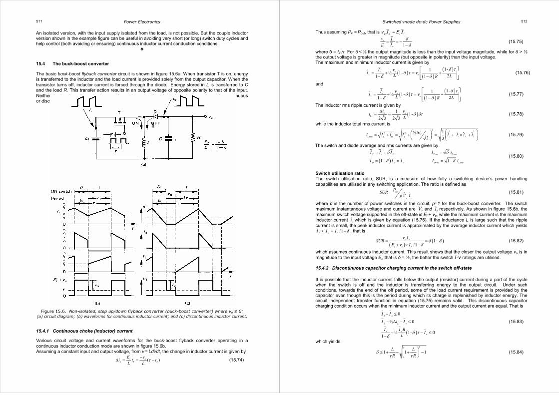
♣ 15.4 The buck-boost converter The basic buck-boost flyback converter circuit is shown in figure 15.6a. When transistor T is on, energy is transferred to the inductor and the load current is provided solely from the output capacitor. When the transistor turns off, inductor current is forced through the diode. Energy stored in L is transferred to C and the load R. This transfer action results in an output voltage of opposite polarity to that of the input. Neither the input nor the output current is continuous, although the inductor current may be continuous or discontinuous.
Figure 15.6. Non-isolated, step up/down flyback converter (buck-boost converter) where vo ≤ 0: (a) circuit diagram; (b) waveforms for continuous inductor current; and (c) discontinuous inductor current. 15.4.1 Continuous choke (inductor) current
Various circuit voltage and current waveforms for the buck-boost flyback converter operating in a continuous inductor conduction mode are shown in figure 15.6b. Assuming a constant input and output voltage, from v = Ldi/dt, the change in inductor current is given by
( )i oL T T
E vi t t
L Lτ−
∆ = = − (15.74)
tD tD
Switched-mode dc-dc Power Supplies
512
Thus assuming Pin = Pout, that is ioo iv I E I=
1
o i
oi
v IIE
δδ
= = −−
(15.75)
where δ = tT /τ. For δ < ½ the output magnitude is less than the input voltage magnitude, while for δ > ½ the output voltage is greater in magnitude (but opposite in polarity) than the input voltage. The maximum and minimum inductor current is given by
( ) ( )( )1-1
½ 1-21 1
δ τδ τ
δ δ∧ = + = +
− − L
o oo
I vi v
L LR (15.76)
and
( ) ( )( )1-1
½ 1-21 1
δ τδ τ
δ δ
∨ = − = −
− − L
o oo
I vi v
L LR (15.77)
The inductor rms ripple current is given by
( ). .
r
11-
2 3 2 3δ δτ
∆= = oL
L
vii
L (15.78)
while the inductor total rms current is
.
2 2 22 2 2
rms r
1½3 3
∧ ∧ ∆= + = + = + × + L LL
LLL L L L
ii I i I i i i i∨ ∨
(15.79)
The switch and diode average and rms currents are given by
( )1 1
T i L Trms L rms
D L o Drms L rms
I I I I i
I I I I i
δ δ
δ δ
= = =
= − = = − (15.80)
Switch utilisation ratio The switch utilisation ratio, SUR, is a measure of how fully a switching device’s power handling capabilities are utilised in any switching application. The ratio is defined as
out
TT
PSURp V I
= (15.81)
where p is the number of power switches in the circuit; p=1 for the buck-boost converter. The switch maximum instantaneous voltage and current are
TV and
TI respectively. As shown in figure 15.6b, the
maximum switch voltage supported in the off-state is Ei + vo, while the maximum current is the maximum inductor current Li
∧which is given by equation (15.76). If the inductance L is large such that the ripple
current is small, the peak inductor current is approximated by the average inductor current which yields /1T oLI I I δ≈ = − , that is
( )
( )1/1
oo
oi o
v ISUR
E v Iδ δ
δ= = −
+ × − (15.82)
which assumes continuous inductor current. This result shows that the closer the output voltage vo is in magnitude to the input voltage Ei, that is δ = ½, the better the switch I-V ratings are utilised. 15.4.2 Discontinuous capacitor charging current in the switch off-state It is possible that the inductor current falls below the output (resistor) current during a part of the cycle when the switch is off and the inductor is transferring energy to the output circuit. Under such conditions, towards the end of the off period, some of the load current requirement is provided by the capacitor even though this is the period during which its charge is replenished by inductor energy. The circuit independent transfer function in equation (15.75) remains valid. This discontinuous capacitor charging condition occurs when the minimum inductor current and the output current are equal. That is
( )
0
½ 0
½ 1- 01
oL
oLL
o oo
I I
I i I
I I RI
Lδ τ
δ
∨
− ≤
− ∆ − ≤
− − ≤−
(15.83)
which yields
2
1 1 1L L
R Rδ
τ τ ≤ + − + −
(15.84)

Power Electronics 513
15.4.3 Discontinuous choke current The onset of discontinuous inductor operation occurs when the minimum inductor current Li
∨, reaches
zero. That is, with 0Li∨= in equation (15.77), the last equality
( )
( )1-10
21 LR
δ τδ
− =−
(15.85)
relates circuit component values (R and L) and operating conditions (f and δ) at the verge of discontinuous inductor current. The change from continuous to discontinuous inductor current conduction occurs when
LL LI i i∧
= = ∆½ ½ (15.86)
where from equation (15.74) ( ) /L o Ti v t Lτ
∧= −
The circuit waveforms for discontinuous conduction are shown in figure 15.6c. The output voltage for discontinuous conduction is evaluated from
( )Li o
T x
E vi t t t
L Lτ
∧= = − − − (15.87)
which yields
1
o
xi
vtE
δ
δ τ
= −− −
(15.88)
Alternatively, using equation (15.87) and
δ∧
= ½ LiI i (15.89)
yields
2
2
τδ= i
i
EI
L (15.90)
The inductor current is neither the input current nor the output current, but is comprised of components (in time) of each of these currents. Examination of figure 15.6b, reveals that these currents are a proportion of the inductor current dependant on the duty cycle, and that on the verge of discontinuous conduction:
δ δ∧ ∧ ∧
= = = ∆½ ½and whereL L Li o off LI i I i i i
Thus using power in equals power out, that is ,=i i o oE I v I equation (15.90) becomes
2 2
22 2o i o
i o i
v E v R
E LLI LI
τδ τδ τδ= = = (15.91)
On the verge of discontinuous conduction, these equations can be rearranged to give
2(1 ) (1 )2 2
τδ δ τ δ= − = −i oo
E vI
L L (15.92)
At a low output current or low input voltage there is a likelihood of discontinuous conduction. To avoid this condition, a larger inductance value is needed, which worsen the transient response. Alternatively, with extremely low on-state duty cycles, a voltage-matching transformer can be used to increase δ. Once a transformer is employed, any smps technique can be used to achieve the desired output voltage. Figures 15.6b and c show that both the input and output current are always discontinuous. 15.4.4 Load conditions for discontinuous inductor current As the load current decreases, the inductor average current also decreases, but the inductor ripple current magnitude is unchanged. If the load resistance is increased sufficiently, the bottom of the triangular inductor current, Li
∨, eventually reduces to zero. Any further increase in load resistance
causes discontinuous inductor current and the voltage transfer function given by equation (15.75) is no longer valid and equations (15.87) and (15.91) are applicable. The critical load resistance for continuous inductor current is specified by
ocrit
o
vR
I≤ (15.93)
Switched-mode dc-dc Power Supplies
514
Substituting for, the average input current in terms of Li∧
and vo in terms of ∆iL from equation (15.74) , yields
2
2
(1 )o
crit
o
v LR
I τ δ≤ =
− (15.94)
By substituting the switching frequency ( 1/sf τ= ) or the fundamental inductor reactance ( 2L sX f Lπ= ) the following critical resistance forms result.
2 2 2
22 2( )
(1 ) (1 ) (1 ) (1 )τ δ τδ δ δ π δ≤ = = × = = Ω
− − − −o o s L
crit
io
v v f L XL LR
EI (15.95)
Equation (15.95) is equation (15.85), re-arranged. If the load resistance increases beyond Rcrit, the output voltage can no longer be maintained with duty cycle control according to the voltage transfer function in equation (15.75). 15.4.5 Control methods for discontinuous inductor current Once the load current has reduced to the critical level as specified by equation (15.95), the input energy is in excess of the load requirement. Open loop load voltage regulation control is lost and the capacitor C tends to overcharge.
Hardware approaches can be used to solve this problem – by ensuring continuous inductor current • increase L thereby decreasing the inductor current ripple p-p magnitude • step-down transformer impedance matching to effectively reduce the apparent load impedance
Two control approaches to maintain output voltage regulation when R > Rcrit are
• vary the switching frequency fs, maintaining the switch on-time tT constant so that ∆iL is fixed or • reduce the switch on-time tT , but maintain a constant switching frequency fs, thereby reducing ∆iL.
If a fixed switching frequency is desired for all modes of operation, then reduced on-time control, using output voltage feedback, is preferred. If a fixed on-time mode of control is used, then the output voltage is control by inversely varying the frequency with output voltage. 15.4.5i - fixed on-time tT, variable switching frequency fvar The operating frequency fvar is varied while the switch-on time tT is maintained constant such that the ripple current remains unchanged. Operation is specified by equating the input energy and the output energy, thus maintaining a constant capacitor charge, hence output voltage. That is, equating energies
2
var
1½ o
L i T
vi E t
R f∆ = (15.96)
Isolating the variable switching frequency fvar gives
2
var
1
½
1
o
L i T
s crit
vf
i E t R
f RR
=∆
= ×
var
1f
Rα (15.97)
Load resistance R is not a directly or readily measurable parameter for feedback proposes. Alternatively, since o ov I R= , substitution for R in equation (15.97) gives
var
var
crits o
o
o
Rf f I
v
f Iα
= × (15.98)
That is, for discontinuous inductor current, namely ½ /< ∆ <orL L o o critI i I v R , if the switch on-state period tT remains constant and fvar is either varied proportionally with load current or varied inversely with load resistance, then the required output voltage vo will be maintained. 15.4.5ii - fixed switching frequency fs, variable on-time tTvar The operating frequency fs remains fixed while the switch-on time tTvar is reduced such that the ripple current can be reduced. Operation is specified by equating the input energy and the output energy as in equation (15.96), thus maintaining a constant capacitor charge, hence voltage. That is

Power Electronics 515
2
var
1½ o
L i T
s
vi E t
R f∆ = (15.99)
Isolating the variable on-time tTvar gives
2
var
1
½o
T
L i s
vt
i E f R=
∆
Substituting ∆iL from equation (15.74) gives
.
.
var
var
1
1
T T crit
T
t t RR
tR
α
= × (15.100)
Again, load resistance R is not a directly or readily measurable parameter for feedback proposes and substitution of /o ov I for R in equation (15.71) gives
.
.
var
var α
= ×critT T o
o
T o
Rt t I
v
t I
(15.101)
That is, if the switching frequency fs is fixed and switch on-time tT is reduced proportionally to . oI or inversely to .R , when discontinuous inductor current commences, namely /< ∆ <orL L o o critI i I v R½ , then the required output voltage magnitude vo will be maintained.
Alternatively the output voltage is related to the duty cycle by / 2δ τ= −o iv E R L . See table 15.2. 15.4.6 Output ripple voltage The output ripple voltage is the capacitor ripple voltage. Ripple voltage for a capacitor is defined as
1o Cv i dt∆ = ∫
Figure 15.6 shows that the constant output current oI is provided solely from the capacitor during the on period tT when the switch conducting, thus
1 1∆ = =∫ oo TC Cv i dt t I
Substituting for /o oI v R= gives
1 1 1∆ = = =∫ ooo T TC C C
vv i dt t tI R
Rearranging gives the percentage peak-to-peak voltage ripple in the output voltage
1 δ τ∆= =o
T
oC CR R
vt
v (15.102)
The capacitor equivalent series resistance and inductance can be account for, as with the forward converter, 15.1.5. When the switch conducts, the output current is constant and is provided solely from the capacitor. Thus no ESL voltage effects result during this constant capacitor current portion of the switching cycle. 15.4.7 Buck-boost, flyback converter design procedure The output voltage of the buck-boost converter can be regulated by operating at a fixed frequency and varying the transistor on-time tT. However, the output voltage diminishes while the transistor is on and increases when the transistor is off. This characteristic makes the converter difficult to control on a fixed frequency basis. A simple approach to control the flyback regulator in the discontinuous mode is to fix the peak inductor current, which specifies a fixed diode conduction time, tD. Frequency then varies directly with output current and transistor on-time varies inversely with input voltage. With discontinuous inductor conduction, the worst-case condition exists when the input voltage is low while the output current is at a maximum. Then the frequency is a maximum and the dead time tx is zero because the transistor turns on as soon as the diode stops conducting.
(min) (max) (min)
(max) (max)
= 0
=
∆ =
Given Worst case
i o i i x
o o o o
E I E E t
V f e I I
Assuming a fixed peak inductor current ii∧
and output voltage vo, the following equations are valid
Switched-mode dc-dc Power Supplies
516
(min) ii T o DE t v t i L∧
= = × (15.103)
(min) (max) 1/ fτ = (15.104)
Equation (15.103) yields
(max)
(min)
1
( 1)D
o
i
tv
fE
=+
(15.105)
Where the diode conduction time tD is constant since in equation (15.103), v0, ii∧
, and L are all constants. The average output capacitor current is given by
(1 )ioI i δ∧
= −½
and substituting equation (15.105) yields
(max) (max)
(max)
(min)
1
( 1)io
o
i
I i fv
fE
∧× ×
+= ½
therefore
(max)
(min)
2 ( 1)io
o
i
vi I
E
∧= × × +
and upon substitution into equation (15.103)
(max)
(min)
2 ( 1)
D o
oo
i
t vL
vI
E
=+
(15.106)
The minimum capacitance is specified by the maximum allowable ripple voltage, that is
2
∧∨ ∆= =∆ ∆
i D
o o
i tQC
e e
that is
(max)
(min)
( 1)
∨
=∆ +
o D
oo
i
I tC
ve
E
(15.107)
For large output capacitance, the ripple voltage is dropped across the capacitor equivalent series resistance, which is given by
(max)
i
oeESR
i∧
∆= (15.108)
The frequency varies as a function of load current. Equation (15.104) gives
(max)
(max)
½∧
= =i
ooT
IIi t
f f
therefore
(max)
(max)
o
o
If f
I= × (15.109)
and
(min)
(min) (max)
(max)
o
o
If f
I= × (15.110)
Example 15.4: Buck-boost flyback converter The 10kHz flyback converter in figure 15.6 is to operate from a 50V input and produces an inverted non-isolated 75V output. The inductor is 300µH and the resistive load is 2.5Ω.
i. Calculate the duty cycle, hence transistor off-time, assuming continuous inductor current. ii. Calculate the mean input and output current. iii. Draw the inductor current, showing the minimum and maximum values. iv. Calculate the capacitor rms ripple current and output p-p ripple voltage if C = 10,000µF. v. Determine
• the critical load resistance. • the minimum inductance for continuous inductor conduction with 2.5 Ω load

Power Electronics 517
vi. At what load resistance does the instantaneous inductor current fall below the output current? vii. What is the output voltage if the load resistance is increased to four times the critical resistance?
Solution i. From equation (15.88), which assumes continuous inductor current
/1
δ δ τδ
= − =−
whereoT
i
vt
E
that is
35
75V
50V 1
δ δδ
= =−
thus
That is, τ = 1/ fs = 100 µs with a 60µs switch on-time.
ii. The mean output current oI is given by
/ 75V/2.5Ω = 30Ao oI v R= =
From power transfer considerations / 75V×30A/50V = 45Ai L o o iI I v I E= = =
iii. The average inductor current can be derived from 1- ) δ δ= =(ori L o LI I I I
That is
3 2
5 5
/ /(1- )
= 45A/ = 30A/ = 75AL i oI I Iδ δ= =
From v = L di/dt, the ripple current ∆iL = Ei tT /L = 50V x 60µs /300 µH = 10 A, that is
½ 75A + ½×10A = 80A
½ 75A - ½×10A = 70A
L
L
L L
L L
i I i
i I i
∧= + ∆ =
= − ∆ =∨
Since 70A 0A,Li∨
= ≥ rhe inductor current is continuous, thus the analysis in parts i, ii, and iii, is valid. iv. The capacitor current is derived by using Kirchhoff’s current law such that at any instant in time, the diode current, plus the capacitor current, plus the 30A constant load current into R, all sum to zero.
.
.
2 2
rms 0 0
60 µs 40 µs2 2
0 0
1( )
1 10A30A ( 50A) = 36.8A
100µs 40µs
T T
L
t tL
C o oT
ii I dt t i I dtt
dt t dt
τ
τ τ− ∧ ∆
= + − + −
= + −
∫ ∫
∫ ∫
Figure: Example 15.4
10A
IT ID IT ID
IL=75A
60µs
Io=30A
iC (A)
30
0
40
50
0 50 100 150 t (µs)
0 50 100 150 t (µs)
iL (A)
80
75
70
1.8mC
1.8mC
Switched-mode dc-dc Power Supplies
518
The output ripple voltage is given by equation (15.102), that is
3
5 100µs0.24%
10,000µF 2½o
o
v
v CR
δτ∆ ×= = ≡
× Ω
The output ripple voltage is therefore 20.24 10 75V 180mVov −∆ = × × =
v. The critical load resistance, Rcrit, produces an inductor current with ∆iL = 10 A ripple. From equation (15.95)
2 23
5
2 2×300µH = 37½Ω
(1 ) 100µs (1- )crit
LR
τ δ= =
− ×
The minimum inductance for continuous inductor current operation, with a 2½Ω load, can be found by rearranging the critical resistance formula, as follows: 2 23
5(1 ) = ½×2.5Ω×100µs×(1- ) = 20µHcritL Rτ δ= −½
vi. The ± 5A inductor ripple current is independent of the load, provided the critical resistance of 37½Ω is not exceeded. When the average inductor current is less than 5A more than the output current, the capacitor must provide load current not only when the switch is on but also for a portion of the time when the switch is off. The transition is given by equation (15.84), that is
2
1 1 1L L
R Rδ
τ τ ≤ + − + −
Alternately, when
5A
5A1
oi
oo
I I
II
δ
− =
− =−
For δ = ⅗, oI = 3⅓A. whence
10
3
75V22½
A= = = Ωo
o
vR
I
The average inductor current is 8⅓A, with a minimum value of 3⅓A, the same as the load current. That is, for R < 22½Ω all the load requirement is provided from the inductor when the switch is off, with excess energy charging the output capacitor. For R > 22½Ω insufficient energy is available from the inductor to provide the load energy throughout the whole of the period when the switch is off. The capacitor supplements the load requirement towards the end of the off period. When R > 37½Ω (the critical resistance), discontinuous inductor current occurs, and the purely duty cycle dependent transfer function (circuit parameter independent) is no longer valid. vii. When the load resistance is increased to 150Ω, four times the critical resistance, the output voltage is given by equation (15.91):
35
100µs 15050V 150V
2 2 300µH
τδ × Ω= = × =
××o i
Rv E
L
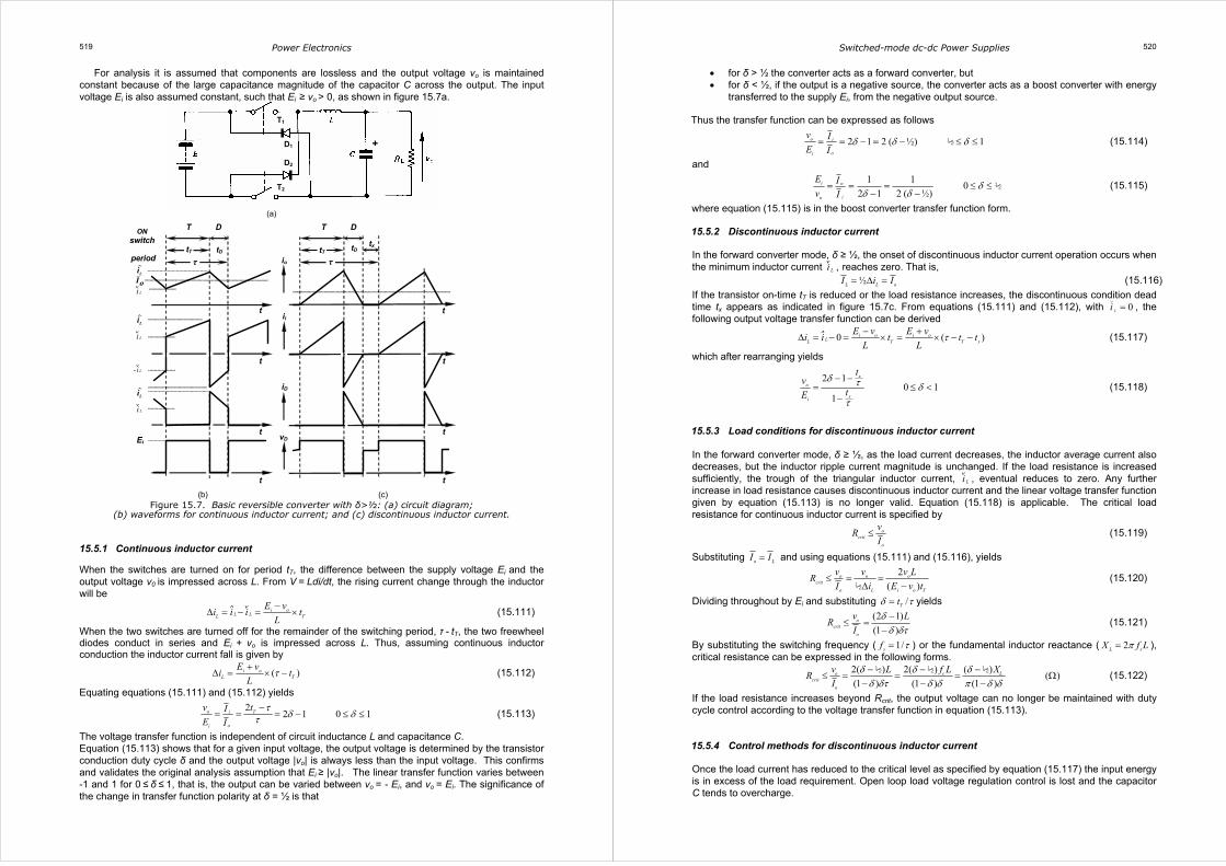
♣ 15.5 The output reversible converter The basic reversible converter, sometimes called an asymmetrical half bridge converter (see chapter 13.5), shown in figure 15.7a allows two-quadrant output voltage operation. Operation is characterised by both switches operating simultaneously, being either both on or both off.
The input voltage Ei is chopped by switches T1 and T2, and because the input voltage is greater than the load voltage vo, energy is transferred from the dc supply Ei to L, C, and the load R. When the switches are turned off, energy stored in L is transferred via the diodes D1 and D2 to C and the load R but in a path involving energy being returned to the supply, Ei. This connection feature allows energy to be transferred from the load back into Ei when used with an appropriate load and the correct duty cycle.
Parts b and c respectively of figure 15.7 illustrate reversible converter circuit current and voltage waveforms for continuous and discontinuous conduction of L, in a forward converter mode, when δ > ½.
Power Electronics 519
T1
D1
D2 T2
+
(a)
io
ii
iD
ON switch
period
t t
t t
t
t
T D T D
τ τ tT tT
tx
t
t
vD
IoLi
Li
Li
Li∨
Li∨
Li∨
Ei
- Li∨
(b) (c)
tD tD
For analysis it is assumed that components are lossless and the output voltage vo is maintained constant because of the large capacitance magnitude of the capacitor C across the output. The input voltage Ei is also assumed constant, such that Ei ≥ vo > 0, as shown in figure 15.7a.
Figure 15.7. Basic reversible converter with δ>½: (a) circuit diagram; (b) waveforms for continuous inductor current; and (c) discontinuous inductor current.
15.5.1 Continuous inductor current
When the switches are turned on for period tT, the difference between the supply voltage Ei and the output voltage v0 is impressed across L. From V = Ldi/dt, the rising current change through the inductor will be
i oL LL
E vi i i t
L Τ
−∆ = − = ×
∧ ∨ (15.111)
When the two switches are turned off for the remainder of the switching period, τ - tT, the two freewheel diodes conduct in series and Ei + vo is impressed across L. Thus, assuming continuous inductor conduction the inductor current fall is given by
( )i oL
E vi t
L Ττ+∆ = × − (15.112)
Equating equations (15.111) and (15.112) yields
2
2 1 0 1τ
δ δτ−
= = = − ≤ ≤o Ti
oi
v tIE I
(15.113)
The voltage transfer function is independent of circuit inductance L and capacitance C. Equation (15.113) shows that for a given input voltage, the output voltage is determined by the transistor conduction duty cycle δ and the output voltage |vo| is always less than the input voltage. This confirms and validates the original analysis assumption that Ei ≥ |vo|. The linear transfer function varies between -1 and 1 for 0 ≤ δ ≤ 1, that is, the output can be varied between vo = - Ei, and vo = Ei. The significance of the change in transfer function polarity at δ = ½ is that
Switched-mode dc-dc Power Supplies
520
• for δ > ½ the converter acts as a forward converter, but • for δ < ½, if the output is a negative source, the converter acts as a boost converter with energy
transferred to the supply Ei, from the negative output source. Thus the transfer function can be expressed as follows
2 1 2 ( ½) 1o i
oi
v IE I
δ δ δ= = − = − ≤ ≤½ (15.114)
and
1 1
02 1 2 ( ½)
i o
io
E Iv I
δδ δ
= = = ≤ ≤− −
½ (15.115)
where equation (15.115) is in the boost converter transfer function form. 15.5.2 Discontinuous inductor current In the forward converter mode, δ ≥ ½, the onset of discontinuous inductor current operation occurs when the minimum inductor current Li
∨, reaches zero. That is,
½L L oI i I= ∆ = (15.116)
If the transistor on-time tT is reduced or the load resistance increases, the discontinuous condition dead time tx appears as indicated in figure 15.7c. From equations (15.111) and (15.112), with 0Li
∨= , the
following output voltage transfer function can be derived
0 ( )i o i oLL x
E v E vi i t t t
L LΤ Ττ− +∆ = − = × = × − −
∧ (15.117)
which after rearranging yields
2 1
0 11
x
o
xi
tv
tE
δ τ δτ
− −= ≤ <
− (15.118)
15.5.3 Load conditions for discontinuous inductor current In the forward converter mode, δ ≥ ½, as the load current decreases, the inductor average current also decreases, but the inductor ripple current magnitude is unchanged. If the load resistance is increased sufficiently, the trough of the triangular inductor current, Li
∨, eventual reduces to zero. Any further
increase in load resistance causes discontinuous inductor current and the linear voltage transfer function given by equation (15.113) is no longer valid. Equation (15.118) is applicable. The critical load resistance for continuous inductor current is specified by
ocrit
o
vR
I≤ (15.119)
Substituting o LI I= and using equations (15.111) and (15.116), yields
2
( )o o o
crit
o L i o
v v v LR
I i E v tΤ≤ = =
∆ −½ (15.120)
Dividing throughout by Ei and substituting /Ttδ τ= yields
(2 1)
(1 )o
crit
o
v LR
I
δδ δτ−
≤ =−
(15.121)
By substituting the switching frequency ( 1/sf τ= ) or the fundamental inductor reactance ( 2L sX f Lπ= ), critical resistance can be expressed in the following forms.
2( ) 2( ) ( )
( )(1 ) (1 ) (1 )
o s Lcrit
o
v L f L XR
I
δ δ δδ δτ δ δ π δ δ− − −
≤ = = = Ω− − −
½ ½ ½ (15.122)
If the load resistance increases beyond Rcrit, the output voltage can no longer be maintained with duty cycle control according to the voltage transfer function in equation (15.113). 15.5.4 Control methods for discontinuous inductor current Once the load current has reduced to the critical level as specified by equation (15.117) the input energy is in excess of the load requirement. Open loop load voltage regulation control is lost and the capacitor C tends to overcharge.
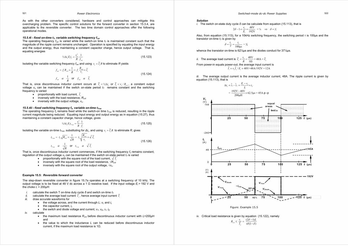
Power Electronics 521
As with the other converters considered, hardware and control approaches can mitigate this overcharging problem. The specific control solutions for the forward converter in section 15.3.4, are applicable to the reversible converter. The two time domain control approaches offer the following operational modes. 15.5.4i - fixed on-time tT, variable switching frequency fvar The operating frequency fvar is varied while the switch-on time tT is maintained constant such that the magnitude of the ripple current remains unchanged. Operation is specified by equating the input energy and the output energy, thus maintaining a constant capacitor charge, hence output voltage. That is, equating energies
2
var
1½ o
L i T
vi E t
R f∆ = (15.123)
Isolating the variable switching frequency fvar and using o ov I R= to eliminate R yields
var
var var
1
1
crits crit s o
o
o
Rf f R f I
vR
f f IR
α α
= × = ×
or
(15.124)
That is, once discontinuous inductor current occurs at ½ /< ∆ <oro L o o critI i I v R , a constant output voltage vo can be maintained if the switch on-state period tT remains constant and the switching frequency is varied
• proportionally with load current, oI • inversely with the load resistance, Rcrit • inversely with the output voltage, vo.
15.5.4ii - fixed switching frequency fs, variable on-time tTvar The operating frequency fs remains fixed while the switch-on time tTvar is reduced, resulting in the ripple current magnitude being reduced. Equating input energy and output energy as in equation (15.27), thus maintaining a constant capacitor charge, hence voltage, gives
2
var
1½ o
L i T
s
vi E t
R f∆ = (15.125)
Isolating the variable on-time tTvar, substituting for ∆iL, and using o ov I R= to eliminate R, gives
.
.
.
.
var
var var
1
1α α
= × = ×
or
critT T crit T o
o
T T o
Rt t R t I
vR
t t IR
(15.126)
That is, once discontinuous inductor current commences, if the switching frequency fs remains constant, regulation of the output voltage vo can be maintained if the switch on-state period tT is varied
• proportionally with the square root of the load current, . oI • inversely with the square root of the load resistance, √Rcrit • inversely with the square root of the output voltage, √vo.
Example 15.5: Reversible forward converter
The step-down reversible converter in figure 15.7a operates at a switching frequency of 10 kHz. The output voltage is to be fixed at 48 V dc across a 1 Ω resistive load. If the input voltage Ei = 192 V and the choke L = 200µH:
i. calculate the switch T on-time duty cycle δ and switch on-time tT ii. calculate the average load current oI , hence average input current iI iii. draw accurate waveforms for
• the voltage across, and the current through L; vL and iL • the capacitor current, ic • the switch and diode voltage and current; vT, vD, iT, iD
iv. calculate • the maximum load resistance Rcrit before discontinuous inductor current with L=200µH
and • the value to which the inductance L can be reduced before discontinuous inductor
current, if the maximum load resistance is 1Ω.
Switched-mode dc-dc Power Supplies
522
Solution i. The switch on-state duty cycle δ can be calculate from equation (15.113), that is
58
48V2 1 = ¼
192Vo
i
v
Eδ δ− = = ⇒ =
Also, from equation (15.113), for a 10kHz switching frequency, the switching period τ is 100µs and the transistor on-time tT is given by
58 =
100µsδ τ= =T Tt t
whence the transistor on-time is 62½µs and the diodes conduct for 37½µs.
ii. The average load current is 48V
= 48A =1Ω
oo L
vI I
R= =
From power-in equals power-out, the average input current is / 48V×48A/192V = 12Ai o o iI v I E= =
iii. The average output current is the average inductor current, 48A. The ripple current is given by equation (15.113), that is
192V - 48V
= 62.5µs = 45A 200µH
Τ
−∆ = − = ×
× p -p
i oL LL
E vi i i t
L
∧ ∨
iv. Critical load resistance is given by equation (15.122), namely
(2 1)
(1 )o
crit
o
v LR
I
δτδ δ
−≤ =
−
(V) (A)
VDiode
VTran
VTran
VDiode
Icap
equal areas
192V
0 25 50 75 100 125 t (µs)
0 25 50 75 100 125 t (µs)
0 25 50 75 100 125 t (µs)
VL (V)
144
-240
IL (A)
48
0
62½
45A Iave
Figure: Example 15.5
9mV.s
22½A -

Power Electronics 523
58
5 58 8
215
(2 -1)×200µH= 32/15
100µs (1- )
= 2 Ω ½ 22 A
×= Ω
× ×
= ∆ = ½when o LI i
Alternatively, the critical load current is 22½A (½∆iL), thus the load resistance must not be greater than /o ov I = 48V/22.5A = 32/15Ω, if the inductor current is to be continuous.
The critical resistance formula given in equation (15.122) is valid for finding critical inductance when inductance is made the subject of the equation, that is, rearranging equation (15.122) gives
5 5 58 8 8
= (1 ) /(2 1) (H)
= 1Ω×(1- )× ×100µs/(2× -1)
= 93 µH
critL R δ δ τ δ× − × × −
¾
That is, the inductance can be decreased from 200µH to 93¾µH when the load is 1Ω and continuous inductor current will flow.
♣ 15.5.5 Comparison of the reversible converter with alternative converters The reversible converter provides the full functional output range of the forward converter when δ > ½ and provides part of the voltage function of the buck-boost converter when δ < ½ but with energy transferring in the opposite direction.
Comparison of example 15.1 and 15.4 shows that although the same output voltage range can be achieved, the inductor ripple current is much larger for a given inductance L. A similar result occurs when compared with the buck-boost converter. Thus in each case, the reversible converter has a narrower output resistance range before discontinuous inductor conduction occurs. It is therefore concluded that the reversible converter should only be used if two quadrant operation is needed.
The ripple current fI∼
given by equation (15.2) for the forward converter and equation (15.111) for the reversible converter when vo > 0, yield the following current ripple relationship.
(2 1/ )
2 1 0 1 1f r r
r f f r
I Iδ
δ δ δ δ
= − ×
− = ≤ ≤ ≤ ≤½where for and (15.127)
This equation shows that the ripple current of the forward converter fI∼
is never greater than the ripple current rI
∼
for the reversible converter, for the same output voltage. In the voltage inverting mode, from equations (15.74) and (15.111), the relationship between the two corresponding ripple currents is given by
2( 1)
2 1
2( 1) 0 0
2 1
rfly r
r
rfly fly r
r
I Iδδ
δδ δ δ
δ
−= ×
−−
= ≤ ≤ ≤ ≤−
½ ½where for and
(15.128)
Again the reversible converter always has the higher inductor ripple current. Essentially the higher ripple current results in each mode because the inductor energy release phase involving the diodes, occurs back into the supply, which is effectively in cumulative series with the output capacitor voltage.
The reversible converter offers some functional flexibility, since it can operate as a conventional forward converter, when only one of the two switches is turned off. (In fact, in this mode, switch turn-off is alternated between T1 and T2 so as to balance switch and diode losses.) 15.6 The Ćuk converter The Ćuk converter in figure 15.8 performs an inverting boost converter function with inductance in the input and the output. As a result, both the input and output currents can be continuous. A capacitor is used in the process of transferring energy from the input to the output and ac couples the input boost converter stage (L1, T) to the output forward converter (D, L2). Specifically, the capacitor C1 ac couples the switch T in the boost converter stage into the output forward converter stage. 15.6.1 Continuous inductor current When the switch T is on and the diode D is reversed biased 1( ) 2C on L oi I I= − = (15.129)
When the switch is turned off, inductor currents iL1 and iL2 are divert through the diode and 1(off)C ii I= (15.130)
Switched-mode dc-dc Power Supplies
524
vo
L1 L2
+
C1
C2
Figure 15.8. Basic Ćuk converter. Over one steady-state cycle the average capacitor charge is zero, that is 1(on) 1(off) (1 ) 0C Ci iδτ δ τ+ − = (15.131)
which gives
1(on)
1(off) (1 )C i
C o
i I
i I
δδ
= =−
(15.132)
From power-in equals power-out
1
2
o i L
i o L
v I I
E I I= = (15.133)
Thus equation (15.132) becomes
1
2 (1 )o i L
i o L
v I I
E I I
δδ
= = = −−
(15.134)
15.6.2 Discontinuous inductor current The current rise in L1 occurs when the switch is on, that is
1
1
iL
Ei
L
δτ∆ = (15.135)
For continuous current in the input inductor L1, 1 1i L LI I i= ≥ ∆½ (15.136)
which yields a maximum allowable load resistance, for continuous inductor current, of
11 1
2 2 2
22
(1 ) (1 ) (1 )o s L
crit
o
v f LL XR
I
δδ δτ δ δ π δ
≤ = = =− − −
(15.137)
This is the same expression as that obtained for the boost converter, equation (15.66), which can be re-arranged to give the minimum inductance for continuous input inductor current, namely
( )2
1
1
2
RL
δ τδ
∨ −= (15.138)
The current rise in L2 occurs when the switch is on and the inductor voltage is Ei, that is
2
2
iL
Ei
L
δτ∆ = (15.139)
For continuous current in the output inductor L2, 2 2o L LI I i= ≥ ∆½ (15.140)
which yields
222 22
(1 ) (1 ) (1 )Lo s
crit
o
Xv f LLR
I τ δ δ π δ≤ = = =
− − − (15.141)
This is the same expression as that obtained for the forward converter, equation (15.26) which can be re-arranged to give the minimum inductance for continuous output inductor current, namely
( )2 ½ 1L Rδ τ∨
= − (15.142)

Power Electronics 525
15.6.3 Optimal inductance relationship Optimal inductor conditions are that both inductors should both simultaneous reach the verge of discontinuous conduction. The relationship between inductance and ripple current is given by equations (15.135) and (15.139).
1 2
1 2
i iL L
E Ei i
L L
δτ δτ∆ = ∆ =and
After diving these two equations
2 1
1 2
L
L
L i
L i
∆=∆
(15.143)
Critical inductance is given by equations (15.138) and (15.142), that is
( ) ( )2
2 1
1½ 1
2
δ τδ τ
δ
∨ ∨ −= − =and
RL R L
After dividing
2
11
L
L
δδ
∨
∨ =−
(15.144)
At the verge of simultaneous discontinuous inductor conduction
2 1
21
1oL
L i
viL
i EL
δδ
∨
∨
∆= = =
− ∆ (15.145)
That is, the voltage transfer ratio uniquely specifies the ratio of the minimum inductances and their ripple current. 15.6.3 Output voltage ripple The output stage (L2, C2, and R) is the forward converter output stage; hence the per unit output voltage ripple on C2 is given by equation (15.35), that is
2
2
2 2
18
(1 )C o
o o
v v
v v L C
δ τ∆ ∆ −= = × (15.146)
If the ripple current in L1 is assumed constant, the per unit voltage ripple on the ac coupling capacitor C1
is approximated by
1
1
C
o
v
v RC
δ τ∆= (15.147)
Example 15.6: Ćuk converter The Ćuk converter in figure 15.8 is to operate at 10kHz from a 50V battery input and produces an inverted non-isolated 75V output. The load power is 1.8kW.
i. Calculate the duty cycle hence switch on and off times, assuming continuous current in both inductors.
ii. Calculate the mean input and output, hence inductor, currents. iii. At the 1.8kW load level, calculate the inductances L1 and L2 such that the ripple current is
1A p-p in each. iv. Specify the capacitance for C1 and C2 if the ripple voltage is to be a maximum of 1% of
the output voltage. v. Determine the critical load resistance for which the purely duty cycle dependant voltage
transfer function becomes invalid. vi. At the critical load resistance value, determine the inductance value to which the non-
critically operating inductor can be reduced. vii. Determine the necessary conditions to ensure that both inductors operate simultaneously
on the verge of discontinuous conduction, and the relative ripple currents for that condition.
Solution i. The voltage transfer function is given by equation (15.134), that is
75V
1½(1 ) 50V
o
i
v
E
δδ
= − = − = −−
Switched-mode dc-dc Power Supplies
526
from which 35δ = . For a 10kHz switching frequency the period is 100µs, thus the switch on-time is 60µs
and the off-time is 40µs.
ii. The mean output current is determined by the load and the mean input current is related to the output current by assuming 100% efficiency, that is
2
1
/ 1800W / 75V 24A
/ 1800W / 50V 36A
Lo o o
Li o i
I I P v
I I P E
= = = =
= = = =
The load resistance is therefore R = vo /Io = 75V/24A = 3⅛Ω.
iii. The inductor ripple current for each inductor is given by the same expression, that is equations (15.135) and (15.139). Thus for the same ripple current of 1A pp
1 2
1 2
i iL L
E Ei i
L L
δτ δτ∆ = = ∆ =
which gives
1 2
35 100µs 50V
3mH1A
iEL L
i
δτ × ×= = = =
∆
iv. The capacitor ripple voltages are given by equations (15.147) and (15.146), which after re-arranging gives
1 25
81
2 2
2
2 2
35
351 1
8 8
100 100µs1.92mF
1
(1 ) 100 (1 ) 100µs16.6µF
1 3mH
o
C
o
C
vC
v R
vC
v L
δ τ
δ τ
×= × = × =∆ Ω
− − ×= × × = × × =∆
v. The critical load resistance for each inductor is given by equations (15.137) and (15.141). When both inductors are 3mH:
1
2 2
2
35
35
35
2 2 3mH225
(1 ) 100µs (1 )
2 2 3mH150
(1 ) 100µs (1 )
crit
crit
LR
LR
δτ δ
τ δ
× ×≤ = = Ω
− × −×
≤ = = Ω− × −
The limiting critical load resistance is 150Ω or for Io = vo /R = 75V/150Ω = ½A, when a lower output current results in the current in L2 becoming discontinuous although the current in L1 is still continuous. vi. From equation (15.137), rearranged
2 2
1
35
35
(1 ) 100µs 100 (1 )2mH
2 2crit
RL
τ δδ− × Ω× −
≥ = =×
That is, if L1 is reduced from 3mH to 2mH, then both L1 and L2 enter discontinuous conduction at the same load condition, 75V, ½A, and 150Ω. vii. For both converter inductors to be simultaneously on the verge of discontinuous conduction, equation (15.145) gives
2 1
21
35
3 25 3
1
3mH 1A 75V 3
2mH 1 A 50V 2
oL
L i
viL
i EL
δδ
∨
∨
∆= = =
− ∆
= = = =−
♣ 15.7 Comparison of basic converters The converters considered employ an inductor to transfer energy from one dc voltage level to another dc voltage level. The basic converters comprise a switch, diode, inductor, and a capacitor. The reversible converter is a two-quadrant converter with two switches and two diodes, while the Ćuk converter uses two inductors and two capacitors.
Table 15.1 summarises the main electrical features and characteristics of each basic converter. Figure 15.9 shows a plot of the voltage transformation ratios and the switch utilisation ratios of the converters considered. With reference to figure 15.9, it should be noted that the flyback step-up/step-down converter and the Ćuk converter both invert the input polarity.
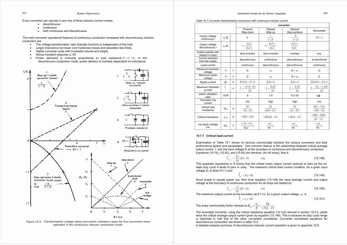
Power Electronics 527
& Cuk
0 ¼ ½ ¾ 1
δ = tT/τ
1
¾
½
¼
Po / PT
step-up 1
step-down3
full bridge
buck-boost /Cuk
2 reversible 4
Every converter can operate in any one of three inductor current modes: • discontinuous • continuous • both continuous and discontinuous
The main converter operational features of continuous conduction compared with discontinuous inductor conduction are
• The voltage transformation ratio (transfer function) is independent of the load. • Larger inductance but lower core hysteresis losses and saturation less likely. • Higher converter costs with increased volume and weight. • Worse transient response (L /R). • Power delivered is inversely proportional to load resistance, 2 /oP V R= . In the
discontinuous conduction mode, power delivery is inversely dependent on inductance.
Figure 15.9. Transformation voltage ratios and switch utilisation ratios for five converters when operated in the continuous inductor conduction mode.
Switched-mode dc-dc Power Supplies
528
Table 15.1 Converter characteristics comparison with continuous inductor current 15.7.1 Critical load current Examination of Table 15.1 shows no obvious commonality between the various converters and their performance factors and parameters. One common feature is the relationship between critical average output current oI and the input voltage Ei at the boundary of continuous and discontinuous conduction. Equations (15.14), (15.62), and (15.92) are identical, (for all smps), that is
(1 ) (A)2critical
io
EI
L
τδ δ= − (15.148)
This quadratic expression in δ shows that the critical mean output current reduces to zero as the on-state duty cycle δ tends to zero or unity. The maximum critical load current condition, for a given input voltage Ei, is when δ = ½ and
/ 8τ= iI E Lco (15.149)
Since power in equals power out, then from equation (15.148) the input average current and output voltage at the boundary of continuous conduction for all smps are related by
(1 ) (A)2critical
oi
vI
L
τδ δ= − (15.150)
The maximum output current at the boundary (at δ = ½), for a given output voltage, vo, is
/ 8τ= oI v Lci
(15.151)
The smps commonality factor reduces to( )21
ocrit
i
v LRE τ δ δ
= ×−
.
The reversible converter, using the critical resistance equation (15.122) derived in section 15.5.3, yields twice the critical average output current given by equation (15.148). This is because its duty cycle range is restricted to half that of the other converters considered. Converter normalised equations for discontinuous conduction are shown in table 15.2. A detailed analysis summary of discontinuous inductor current operation is given in appendix 15.9.
converter Forward
Step-down Flyback Step-up
Flyback Step-up/down
Reversible
Output voltage continuous I
vo /Ei δ 1
1 δ−
1
δδ
−−
2 1δ −
Output voltage discontinuous I
vo /Ei 2
21 i
i
LI
Eδ τ−
2
12
i T
o
E t
IL
δ+
2
2i
o
E
LI
δ τ
Output polarity with respect to input
Non-inverted Non-inverted inverted any
Current sampled from the supply
discontinuous continuous discontinuous bi-directional
Load current continuous discontinuous discontinuous continuous
Maximum transistor voltage
V V Ei vo Ei + vo Ei
Maximum diode voltage
V V Ei vo Ei + vo Ei
Ripple current ∆i A (1 ) /iE Lδτ δ− /iE Lδτ /iE Lδτ 2 (1 ) /iE Lδτ δ−
Maximum transistor current
Ti
A
(1 )
2o
o
vI
L
τ δ−+
2i
i
EI
L
τδ+
2i
L
EI
L
τδ+
( )
2i o
o
E vI
L
τδ−+
switch utilisation ratio
SUR δ 1-δ δ (1-δ)
Transistor rms current
low high high low
Critical load resistance
Rcrit Ω 2
(1 )
L
τ δ−
2
2
(1 )
L
τδ δ−
2
2
(1 )
L
τ δ−
2( )
(1 )
Lδτδ δ
−−½
Critical inductance Lcrit H ½ (1 )R δ τ− 2(1 )Rτδ δ−½ 2(1 )Rτ δ−½ (1 )
( )
R δ δτδ−−
½½
o/p ripple voltage p-p ∆vo V
( )2 1
8 ovLC
τ δ− ov
RC
τ δ ov
RC
τ δ ov
RC
τ δ
½δ
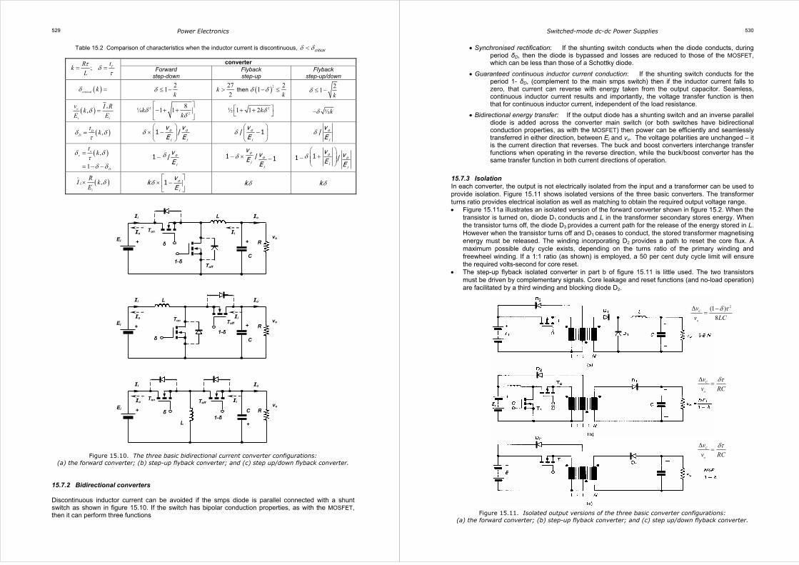
Power Electronics 529
Table 15.2 Comparison of characteristics when the inductor current is discontinuous, criticalδ δ<
converter ;
τ δτ
= = TtRk
L Forward
step-down Flyback step-up
Flyback step-up/down
( )δ =critical k 2
1δ ≤ −k
( )227 2 1
2δ δ> − ≤thenk
k
21δ ≤ −
k
( ),δ =oo
i i
v I Rk
E E
2
2
8¼ 1 1δ
δ − + +
kk
2½ 1 1 2 δ + + k ½δ− k
( ),δ δτ
= DD
tk 1 /o o
i i
v vE E
δ
× −
/ 1o
i
vE
δ
−
/ o
i
vE
δ
( ),
1
δ δτδ δ
=
= − −
xx
D
tk
1 / o
i
vE
δ− 1 / 1o
oi
i
vv
EE
δ− × − 11 /o
o
ii
v vE E
δ
+ −
( ),δ∧
×L
i
RI k
E 1 o
i
vk
Eδ
× −
kδ kδ
Figure 15.10. The three basic bidirectional current converter configurations: (a) the forward converter; (b) step-up flyback converter; and (c) step up/down flyback converter.
15.7.2 Bidirectional converters Discontinuous inductor current can be avoided if the smps diode is parallel connected with a shunt switch as shown in figure 15.10. If the switch has bipolar conduction properties, as with the MOSFET, then it can perform three functions
+ Ei
1-δ
δ vo
R
C
Ton
Toff
+
Ii Io L
Ii Io
+ Ei
1-δ δ
vo R
C
Ton Toff +
Ii Io L
Ii Io
+ Ei
1-δ δ
vo
R C
Ton Toff
+
Ii Io
L
Ii Io
Switched-mode dc-dc Power Supplies
530
2(1 )
8
δ τ∆ −=C
o
v
v LC
δτ∆=C
o
v
v RC
δτ∆=C
o
v
v RC
• Synchronised rectification: If the shunting switch conducts when the diode conducts, during period δD, then the diode is bypassed and losses are reduced to those of the MOSFET, which can be less than those of a Schottky diode.
• Guaranteed continuous inductor current conduction: If the shunting switch conducts for the period 1- δD, (complement to the main smps switch) then if the inductor current falls to zero, that current can reverse with energy taken from the output capacitor. Seamless, continuous inductor current results and importantly, the voltage transfer function is then that for continuous inductor current, independent of the load resistance.
• Bidirectional energy transfer: If the output diode has a shunting switch and an inverse parallel diode is added across the converter main switch (or both switches have bidirectional conduction properties, as with the MOSFET) then power can be efficiently and seamlessly transferred in either direction, between Ei and vo. The voltage polarities are unchanged – it is the current direction that reverses. The buck and boost converters interchange transfer functions when operating in the reverse direction, while the buck/boost converter has the same transfer function in both current directions of operation.
15.7.3 Isolation In each converter, the output is not electrically isolated from the input and a transformer can be used to provide isolation. Figure 15.11 shows isolated versions of the three basic converters. The transformer turns ratio provides electrical isolation as well as matching to obtain the required output voltage range. • Figure 15.11a illustrates an isolated version of the forward converter shown in figure 15.2. When the
transistor is turned on, diode D1 conducts and L in the transformer secondary stores energy. When the transistor turns off, the diode D3 provides a current path for the release of the energy stored in L. However when the transistor turns off and D1 ceases to conduct, the stored transformer magnetising energy must be released. The winding incorporating D2 provides a path to reset the core flux. A maximum possible duty cycle exists, depending on the turns ratio of the primary winding and freewheel winding. If a 1:1 ratio (as shown) is employed, a 50 per cent duty cycle limit will ensure the required volts-second for core reset.
• The step-up flyback isolated converter in part b of figure 15.11 is little used. The two transistors must be driven by complementary signals. Core leakage and reset functions (and no-load operation) are facilitated by a third winding and blocking diode D2.
Figure 15.11. Isolated output versions of the three basic converter configurations:
(a) the forward converter; (b) step-up flyback converter; and (c) step up/down flyback converter.

Power Electronics 531
• The magnetic core in the buck-boost converter of part c of figure 15.11 performs a bifilar inductor function. When the transistor is turned on, energy is stored in the core. When the transistor is turned off, the core energy is released via the secondary winding into the capacitor. A core air gap is necessary to prevent magnetic saturation and an optional clamping winding can be employed, which operates at zero load.
The converters in parts a and c of figure 15.11 provide an opportunity to compare the main features and attributes of forward and flyback isolated converters. In the comparison it is assumed that the transformer turns ratio is 1:1:1. 15.7.3i - The isolated output, forward converter – figure 15.11a:
• δ δ= =oro T i i T ov n E I n I • The magnetic element acts as a transformer, that is, because of the relative voltage polarities of
the windings, energy is transferred from the input to the output, and not stored in the core, when the switch is on. A small amount of magnetising energy, due to the magnetising current to flux the core, is built up in the core.
• The magnetising flux is reset by the current through the catch (feedback) winding and D3, when the switch is off. The magnetising energy is recovered and returned to the supply Ei.
• The necessary transformer Vµs balance requirement (core energy-in equals core energy-out) means the maximum duty cycle is limited to ( )/0 1/ 1 1f bnδ≤ ≤ + < for 1:nf/b:nsec turns ratio. For example, the duty cycle is limited to 50%, 0 ≤ δ ≤ ½, with a 1:1:1 turns ratio.
• Because of the demagnetising winding, the off-state switch supporting voltage is Ei + vo. • The blocking voltage requirement of diode D3 is Ei, vo for D1, and 2Ei for D2. • The critical load resistance for continuous inductor current is independent of the transformer:
( )
41 2crit
LRτ δ
≤−
(15.152)
15.7.3ii - The isolated output, flyback converter – figure 15.11c: • /(1 ) /(1 )δ δ δ δ= − = −oro T i i T ov n E I n I • The magnetic element acts as a magnetic energy storage inductor. Because of the relative
voltage polarities of the windings (dot convention), when the switch is on, energy is stored in the core and no current flows in the secondary.
• The stored energy, which is due to the core magnetising flux is released (reset) as current into the load and capacitor C when the switch is off. (Unlike the forward converter, where magnetising energy is returned to Ei, not the output, vo.) Therefore there is no flyback converter duty cycle restriction, 0 ≤ δ ≤ 1.
• The third winding turns ratio is configured such that energy is only returned to the supply Ei under no load conditions.
• The switch supporting off-state voltage is Ei + vo. • The diode blocking voltage requirements are Ei + vo for D1 and 2Ei for D2. • The critical load resistance for continuous inductor current is independent of the transformer
turns ratio when the magnetising inductance is referenced to the secondary:
( ) ( )
2sec
2 2
44
1 2 1 2T m primm
crit
LLR
η
τ δ τ δ≤ =
− − (15.153)
The operational characteristics of each converter change considerably when the flexibility offered by tailoring the turns ratio is exploited. A multi-winding magnetic element design procedure is outlined in section 9.1.1, where the transformer turns ratio (np :ns) is not necessarily 1:1. The basic approach to any transformer (coupled circuit) problem is to transfer, or refer, all components and variables to either the transformer primary or secondary circuit, whilst maintaining power and time invariance. Thus, maintaining power-in equals power-out, and assuming a secondary to primary turns ratio of nT is to one (nT:1), gives
2
2
T
ps s s s sT T
p p s p p p
iv n n Z nn n n
v n i n Z n
= = = = = =
(15.154)
Time, that is switching frequency, power, and per unit values (δ, ∆vo /vo), are invariant. The circuit is then analysed. Subsequently, the appropriate parameters are referred back to their original side of the magnetically coupled circuit. If the coupled circuit is used as a transformer, magnetising current (flux) builds, which must be reset to
Switched-mode dc-dc Power Supplies
532
1:3
Ei =50V vo = 225V
300µH
Cs
Rs = 22½Ω
iI = 45A
oI =
10A oI =
10A
Ei = 50V 'ov = 75V
300µH Rp = 2½Ω
9Cs
iI = 45A
'
oI =
30A
'
oI =
30A
zero each cycle. Consider the transformer coupled forward converter in figure 15.11a. From Faraday’s equation, /v Nd dtφ= , and for maximum on-time duty cycle δ
∧
the conduction V-µs of the primary must equal the conduction V-µs of the feedback winding which is returning the magnetising energy to the supply Ei.
/
τ= + = and ii on off on off
f b
EE t t t tn (15.155)
That is
( )/
/
/
1
1
1
10
1
ii
f b
f b
f b
EE n
n
n
δ δ
δ
δ
∧ ∧
∧
= −
=+
≤ ≤+
(15.156)
From Faraday’s Law, the magnetizing current starts from zero and increases linearly to
/M i on MI E t L∧
= (15.157)
where LM is the magnetizing inductance referred to the primary. During the switch off period, this current falls linearly, as energy is returned to Ei. The current must reach zero before the switch is turned on again, whence the energy taken from Ei and stored as magnetic energy in the core, has been returned to the supply. Two examples illustrate the features of magnetically coupled circuit converters. Example 15.7 illustrates how the coupled circuit in the flyback converter acts as an inductor, storing energy from the primary source, and subsequently releasing that energy in the secondary circuit. In example 15.8, the forward converter coupled circuit acts as a transformer where energy is transferred through the core under transformer action, but in so doing, self-inductance (magnetising) energy is built up in the core, which must be periodically released if saturation is to be avoided. Relative orientation of the windings, according to the flux dot convention shown in figure 15.11, is thus important, not only the primary relative to the secondary, but also relative to the feedback winding.
Figure 15.12. Isolated output step up/down flyback converter and its equivalent circuit when the output is referred to the primary.
Example 15.7: Transformer coupled flyback converter
The 10kHz flyback converter in figure 15.11c operates from a 50V input and produces a 225V dc output from a 1:1:3 (1:nf/b:nsec) step-up transformer loaded with a 22½Ω resistor. The transformer magnetising inductance is 300µH, referred to the primary:
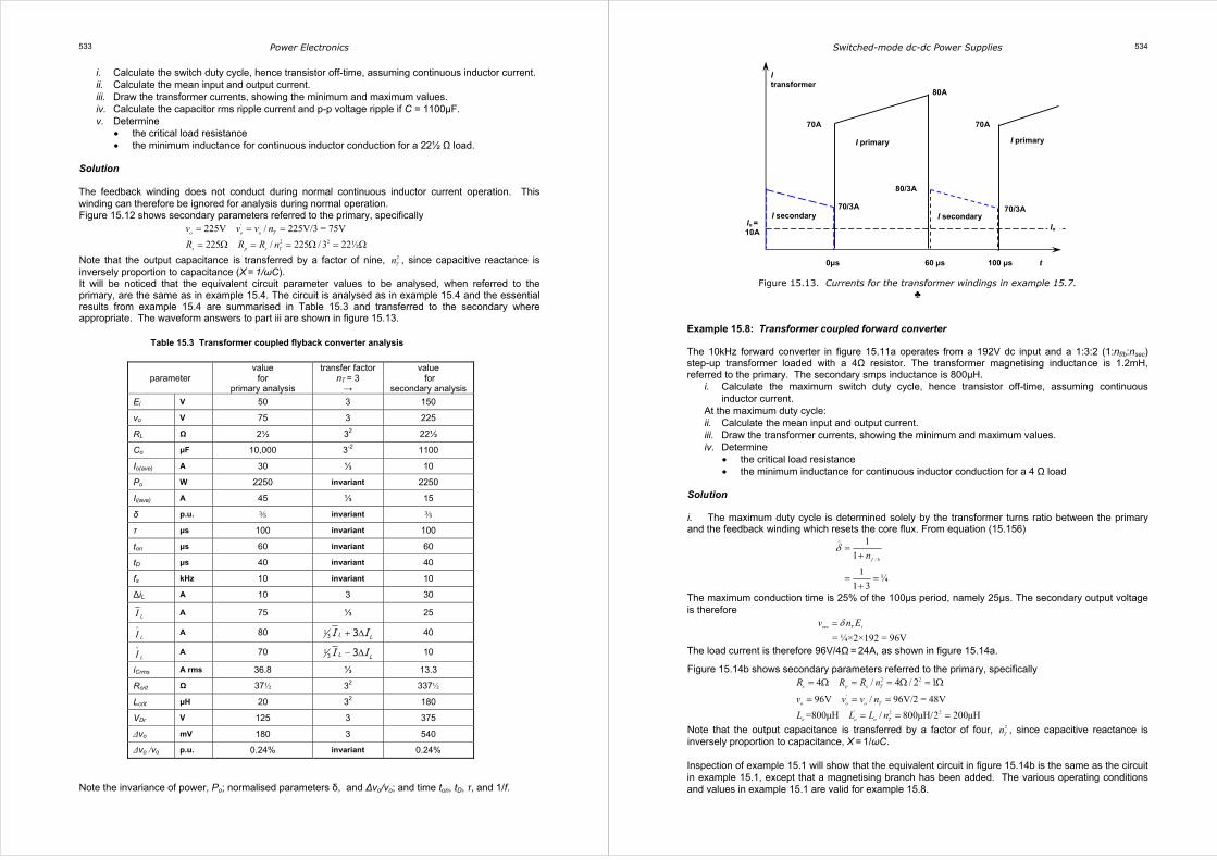
Power Electronics 533
i. Calculate the switch duty cycle, hence transistor off-time, assuming continuous inductor current. ii. Calculate the mean input and output current. iii. Draw the transformer currents, showing the minimum and maximum values. iv. Calculate the capacitor rms ripple current and p-p voltage ripple if C = 1100µF. v. Determine
• the critical load resistance • the minimum inductance for continuous inductor conduction for a 22½ Ω load.
Solution The feedback winding does not conduct during normal continuous inductor current operation. This winding can therefore be ignored for analysis during normal operation. Figure 15.12 shows secondary parameters referred to the primary, specifically
'
2 2
225V / 225V/3 = 75V
225 / 225 / 3 22½o o o T
s p s T
v v v n
R R R n
= = =
= Ω = = Ω = Ω
Note that the output capacitance is transferred by a factor of nine, 2
Tn , since capacitive reactance is inversely proportion to capacitance (X = 1/ωC). It will be noticed that the equivalent circuit parameter values to be analysed, when referred to the primary, are the same as in example 15.4. The circuit is analysed as in example 15.4 and the essential results from example 15.4 are summarised in Table 15.3 and transferred to the secondary where appropriate. The waveform answers to part iii are shown in figure 15.13.
Table 15.3 Transformer coupled flyback converter analysis
parameter value
for primary analysis
transfer factor nT = 3 →
value for
secondary analysis
Ei V 50 3 150
vo V 75 3 225
RL Ω 2½ 32 22½
Co µF 10,000 3-2 1100
Io(ave) A 30 ⅓ 10
Po W 2250 invariant 2250
Ii(ave) A 45 ⅓ 15
δ p.u. ⅗ invariant ⅗
τ µs 100 invariant 100
ton µs 60 invariant 60
tD µs 40 invariant 40
fs kHz 10 invariant 10
∆iL A 10 3 30
LI A 75 ⅓ 25
∧
LI A 80 13 3L LI I+ ∆ 40
LI∨
A 70 13 3L LI I− ∆ 10
iCrms A rms 36.8 ⅓ 13.3
Rcrit Ω 37½ 32 337½
Lcrit µH 20 32 180
VDr V 125 3 375
∆vo mV 180 3 540
∆vo /vo p.u. 0.24% invariant 0.24%
Note the invariance of power, Po; normalised parameters δ, and ∆vo/vo; and time ton, tD, τ, and 1/f.
Switched-mode dc-dc Power Supplies
534
I primary
I secondary I secondary
I primary
80A
70A 70A
70/3A
80/3A
70/3A
0µs 60 µs 100 µs t
I transformer
Io = 10A
Io
Figure 15.13. Currents for the transformer windings in example 15.7. ♣
Example 15.8: Transformer coupled forward converter The 10kHz forward converter in figure 15.11a operates from a 192V dc input and a 1:3:2 (1:nf/b:nsec) step-up transformer loaded with a 4Ω resistor. The transformer magnetising inductance is 1.2mH, referred to the primary. The secondary smps inductance is 800µH.
i. Calculate the maximum switch duty cycle, hence transistor off-time, assuming continuous inductor current.
At the maximum duty cycle: ii. Calculate the mean input and output current. iii. Draw the transformer currents, showing the minimum and maximum values. iv. Determine
• the critical load resistance • the minimum inductance for continuous inductor conduction for a 4 Ω load
Solution i. The maximum duty cycle is determined solely by the transformer turns ratio between the primary and the feedback winding which resets the core flux. From equation (15.156)
/
1
1
1¼
1 3
f bnδ∧
=+
= =+
The maximum conduction time is 25% of the 100µs period, namely 25µs. The secondary output voltage is therefore
sec
= ¼×2×192 = 96VT iv n Eδ=
The load current is therefore 96V/4Ω = 24A, as shown in figure 15.14a.
Figure 15.14b shows secondary parameters referred to the primary, specifically
2 2
'
' 2 2
4 / 4 / 2 1
96V / 96V/2 = 48V
=800µH / 800µH/2 200µH
s p s T
o o o T
o o o T
R R R n
v v v n
L L L n
= Ω = = Ω = Ω
= = =
= = =
Note that the output capacitance is transferred by a factor of four, 2
Tn , since capacitive reactance is inversely proportion to capacitance, X = 1/ωC. Inspection of example 15.1 will show that the equivalent circuit in figure 15.14b is the same as the circuit in example 15.1, except that a magnetising branch has been added. The various operating conditions and values in example 15.1 are valid for example 15.8.

Power Electronics 535
(a)
(b) (c)
Ei=192V
RL=4Ω vo=96V
800µH
10.8mH
24A
9LM
Ei=192V
1.2mH
48A
LM
IM
RL=1Ω vo=48V
Ei=192V
1:3:2
800µH 24A
RL = 4Ω vo = 96V
IM/3
200µH
4C
Figure 15.14. Isolated output forward converter and its equivalent circuits when the output is referred to the primary.
ii. The mean output current is the same for both circuits (example 15.1), 48A, or 24 A when referred to the secondary circuit. The mean input current from Ei remains 12A, but the switch mean current is not 12A. Magnetising current is provided from the supply Ei through the switch, but returned to the supply Ei through diode D2, which bypasses the switch. The net magnetising energy flow is zero. The magnetising current maximum value is given by equation (15.157)
/
192V×25µs/1.2mH = 4A
M i on MI E t L∧
==
This current increases the switch mean current to
= 12A ½ 4A 12½ATI δ+ × × = Figure 15.14c show the equivalent circuit when the switch is off. The output circuit functions independently of the input circuit, which is returning stored core energy to the supply Ei via the feedback winding and diode D2. Parameters have been referred to the feedback winding which has three times the turns of the primary, nf/b =3. The 192V input voltage remains the circuit reference. Equation (15.157)- Faraday’s law, referred to the feedback winding, must be satisfied during the switch off period, that is
2
/ /
2
4 192V×75µs =
3 3 1.2mH
M i off
f b f b M
E tI
n n L
∧
=
×
The diode D2 voltage rating is (nf/b+1)×Ei, 768V and its mean current is
( ) ( )2
/
4A½ 1 ½ 1 - 0.25 = ½A
3M
D
f b
II
nδ= − = × ×
iii. The three winding currents for the transformer are shown in figure 15.15. iv. The critical resistance and inductance, referred to the primary, from example 15.1 are 5⅓Ω and 37½µH. Transforming into secondary quantities, by multiplying by 22, give critical values of RL = 21⅓Ω and L = 150µH.
Switched-mode dc-dc Power Supplies
536
I primary
I secondary
I sec
I primary
61A
39A
57A
39/2A
57/2A
4A 4/3A
0µs 25 µs 100 µs t
I transformer
IM =4A
IM
Figure 15.15. Currents for the three transformer windings in example 15.8. ♣
15.8 Multiple-switch, balanced, isolated converters The basic single-switch converters considered have the limitation of using their magnetic components (whether as an inductor or transformer) only in a unipolar flux mode. Since only one quadrant of the B-H characteristic is employed, these converters are generally restricted to lower powers because of the limited flux swing, which is reduced by the core remanence flux.
The high-power forward converter circuits shown in figure 15.16 operate the magnetic transformer component in the bipolar or push-pull flux mode and require two or four switches. Because the transformers are fully utilised magnetically, they tend to be almost half the size of the equivalent single transistor isolated converter at power levels above 100 W. Also core saturation due to the magnetising current (flux) not being fully reset to zero each cycle, is not a major issue, since with balanced bidirectional fluxing, the average magnetising current (flux) is zero.
15.8.1 The push-pull converter Figure 15.16a illustrates a push-pull forward converter circuit which employs two switches and a centre-tapped transformer. Each switch must have the same duty cycle in order to prevent unidirectional core saturation. Because of transformer coupling action, the off switch supports twice the input voltage, 2Ei, plus any voltage associated with leakage inductance stored energy. Advantageously, no floating gate drives are required and importantly, no switch shoot through (simultaneous conduction) can occur. The voltage transfer function, for continuous inductor conduction, is based on the equivalent secondary output circuit show in figure 15.17. Because of transformer action, the input voltage is N×Ei where N is the transformer turns ratio. When a primary switch is on, current flows in the outer loop shown in figure 15.17. That is
i oL LL
N E vi i i t
L Τ
× −∆ = − = ×
∧ ∨ (15.158)
When the primary switches are off, the secondary voltage falls to zero and current continues to flow through the secondary winding due to the energy stored in L. Efficiency is increased if the diode Df is used to bypass the transformer winding, as shown in figure 15.17. The secondary winding i2R losses are decreased and minimal voltage is coupled from the secondary back into the primary circuit. The current in the inner off loop shown in figure 15.17 is given by
( )oL
vi t
L Ττ∆ = × − (15.159)
Equating equations (15.158) and (15.159) gives the following voltage and current transfer function
2 2 0To i
i o
tv I N NE I
δ δτ= = = ≤ ≤ ½ (15.160)
The output voltage ripple is similar to that of the forward converter
2(1 2 )
32C o
o o
v vv v LC
δ τ∆ ∆ −= = (15.161)

Power Electronics 537
1 N
+ +
N×Ei Ei
off
on Vo
Df
L
Figure 15.16. Multiple-switch, isolated output, pulse-width modulated converters: (a) push-pull; (b) half-bridge; and (c) full-bridge.
Figure 15.17. Equivalent circuit for transformer bridge converters based on a forward converter in the secondary.
2(1 2 )
32
δ τ∆ −=C
o
vv LC
2(1 2 )
16
δ τ∆ −=C
o
vv LC
2(1 2 )
32
δ τ∆ −=C
o
vv LC
C
C
C
Switched-mode dc-dc Power Supplies
538
15.8.2 Bridge converters Figures 15.16b and c show half and full-bridge isolated forward converters respectively. i. Half-bridge In the half-bridge the transistors are switched alternately and must have the same conduction period. This ensures the core volts-second balance requirement to prevent saturation due to bias in one flux direction.
Using similar analysis as for the push-pull converter in 15.8.1, the voltage transfer function of the half bridge with a forward converter output stage, for continuous inductor conduction, is given by
0To i
oi
tv I N NIE
δ δτ= = = ≤ ≤ ½ (15.162)
A floating base drive is required. Although the maximum winding voltage is ½Ei, the switches must support Ei in the off-state, when the complementary switch conducts.
The output ripple voltage is given by
2(1 2 )
16C o
o o
v vv v LC
δ τ∆ ∆ −= = (15.163)
ii. Full-bridge The full bridge in figure 15.16c replaces the capacitor supplies of the half-bridge converter with switching devices. In the off-state each switch must support the rail voltage Ei and two floating gate drive circuits are required. This bridge converter is usually reserved for high-power applications.
Using similar analysis as for the push-pull converter in 15.8.1, the voltage transfer function of the full bridge with a forward converter output stage, with continuous inductor conduction is given by
2 2 0To i
oi
tv I N NIE
δ δτ= = = ≤ ≤ ½ (15.164)
Any volts-second imbalance (magnetising flux build-up) can be minimised by using dc blocking capacitance Cc, as shown in figures 15.16b and c.
The output ripple voltage is given by
2(1 2 )
32C o
o o
v v
v v LC
δ τ∆ ∆ −= = (15.165)
Output stage variations In each forward converter in figure 15.16, a single secondary transformer winding and full-wave rectifier can be used. If the output diode shown dashed in figure 15.16c is used, the off state loop voltage is decreased from two diode voltage drops to one. The three converters in figure 15.16 all employ the same forward converter output stage, so the critical load resistance for continuous inductor current is the same for each case, viz.,
( )
41 2crit
LR
τ δ=
− (15.166)
Re-arrangement of this equation gives an expression for minimum inductance in terms of the load resistance. If the output inductor is not used, conventional unregulated transformer square-wave voltage ratio action occurs for each transformer based smps, where, independent of δ:
o si
ooi
v nI NnE I
= = = (15.167)

Power Electronics 539
15.9 Appendix: Analysis of non-continuous inductor current operation Operation with constant input voltage, Ei In applications were the input voltage Ei is fixed, as with rectifier ac voltage input circuits and battery supplies, the output voltage vo can be controlled by varying the duty cycle. In the continuous inductor conduction region, the transfer function for the three basic converters is determined solely in terms of the on-state duty cycle, δ. Operation in the discontinuous inductor current region, for a constant input voltage, can be characterised for each converter in terms of duty cycle and the normalised output or input current, as shown in figure 15.22. Key region and boundary equations, for a constant input voltage Ei, are summarised in tables 15.4 and 15.5. Operation with constant output voltage, vo In applications were the output voltage vo is fixed, as required with regulated dc power supplies, the effects of varying input voltage Ei can be controlled and compensated by varying the duty cycle. In the inductor continuous current conduction region, the transfer function is determined solely in terms of the on-state duty cycle, δ. Operation in the discontinuous region, for a constant output voltage, can be characterised in terms of duty cycle and the normalised output or input current, as shown in figure 15.23. Key region and boundary equations, for a constant output voltage vo, are summarised in tables 15.6 and 15.7. Because of the invariance of power, the output current oI characteristics for each converter with a constant input voltage Ei , shown in figure 15.22, are the same as those for the input current iI when the output voltage vo is maintained constant, as shown in figure 15.23. [That is the right hand side of each plot in figures 15.22 and 15.23 (or figures 15.18 and 15.21) is the same.] Generalised characteristics, with operating condition k (=Rτ/L), for the three basic converters, are summarised in Table 15.8. The associated monographs in figures 15.24, 15.25, and 15.26, with a specific load condition, k, for each converter, yield the inductor current waveforms for any on-state duty cycle δ. The three graphs illustrate operational boundaries between continuous inductor current at high δ and discontinuous inductor current at lower δ. The graphs for the boost converter in figure 15.25 highlight a little know feature that, if k > 13½, then discontinuous inductor current having appeared, disappears at lower and higher duty cycles. Specifically, continuous inductor current occurs for low duty cycles, where the same theoretical equation is interpreted to the contrary. That is, from table 15.2, the roots of
( )2 21
kδ δ− ≤ (15.168)
are not interpreted correctly. The correct interpretation of δ and k (= Rτ/L) gives:
• for k < 13½, discontinuous inductor current never occurs, independent of δ (equation (15.168) has two imaginary roots)
• for k = 13½, discontinuous inductor current occurs at only δ = ⅓ (equation (15.168) has three roots, two of which are coincident at δ = ⅓)
• for k < 13½, discontinuous inductor current occurs for δ around ⅓ as given by the two (of the three) real roots of equation (15.168) associated with the local minimum turning point of the cubic equation (15.168).
Switched-mode dc-dc Power Supplies
540

Power Electronics 541
0 0.2 0.4 0.6 0.8 1.0
1
0.8
0.6
0.4
0.2
0
δ
/o oI I
0 0.2 0.4 0.6 0.8 1.0
1
0.8
0.6
0.4
0.2
0
δ
/o oI I
0 0.2 0.4 0.6 0.8 1.0
1
0.8
0.6
0.4
0.2
0
δ
/o oI I
1o
i
o
i
v
E
v
E
δ
−
=
discontinuous continuous
( )4 1o
o
I
Iδ δ= − step-up
1
o
i
o
i
v
E
v
E
δ =
−
discontinuous continuous
( )4 1o
o
I
Iδ δ= −
½o
o
o
i
I
I
vE
δ = ×
step-up/down
o
i
v
Eδ =
discontinuous continuous
vo /Ei
45
35
25
15
5
2½
231
1¼ -4
-1½
- 2 3
-¼
( )4 1o
o
I
Iδ δ= −
½1
o
o i
oo
i
v
EI
vIE
δ =
−
× 1,½
1,½
1,½
½ 1o o
io
vIEI
δ = × −
step-down
Figure 15.18. Characteristics for three dc-dc converters with respect to oI ,
when the input voltage Ei is held constant. See table 15.4.
Switched-mode dc-dc Power Supplies
542
Table 15.4. Transfer functions with constant input voltage, Ei, with respect to Io
converter Ei
constant step-down step-up step-up/down
reference equation (15.4) (15.45) (15.75)
o
i
v
Eδ=
1
1o
i
v
E δ=
−
1o
i
v
E
δδ
−=
−
continuous inductor current conduction
(and change of variable) o
i
v
Eδ =
1o
i
o
i
v
Ev
E
δ−
=
1δ =
−
o
i
o
i
v
Ev
E
reference equation (15.21) (15.60) (15.91)
discontinuous inductor current conduction
2
1
21
o
i o
i
v
E LI
Eδ τ
=+
2
12
δ τ= +o i
i o
v E
E LI
2
2o i
i o
v E
E LI
δ τ= −
normalised
=o
i
v
E
where
8iE
IL
τ∧
=o
2
1
11
4
o
i o
v
E I
Iδ ∧
=+ ×
o
21 4 /o o
i
v IE
Iδ
∧= +
o
24 /o o
i
v IE
Iδ
∧= −
o
∧
= =ooI I 1pu @ δ = ½; ½=o
i
v
E δ = ½; 2=o
i
v
E δ = ½; 1= −o
i
v
E
change of variable
∧=o
o
I
I
2
1
4δ∧
−
= ×
o
io
oo
i
v
EIv
IE
2 14
1δ
∧= ×
−
o
oo
i
Iv
IE
2 14δ
∧= − ×o
oo
i
Iv
IE
change of variable δ =
all with a boundary
½ ½ 1δ ∧= + − o
o
I
I
½1
δ ∧= ×−
o
io
o
i
v
EIv
IE
o
½ 1oo
i
vIEI
δ∧
= × −
o
½δ∧
= × oo
i
vIEI o
conduction boundary
½ ½ 1δ ∧= + − o
o
I
I
( )
4 1
4 1δ δ
∧
= × −
= −
o oo
i io
v vIE E
I
( )
2
1
4
4 1δ δ
∧
−
= ×
= −
o
io
oo
i
v
EI
vIE
( )
24
1
4 1δ δ
∧= − ×
−
= −
o
io
oo
i
v
EI
vIE

Power Electronics 543
Figure 15.19. Characteristics for three dc-dc converters with respect to iI ,
when the input voltage Ei is held constant. See table 15.5.
1o
i
o
i
v
E
v
E
δ
−
=
discontinuous continuous
1 o
i i
oi
i
vEI
vIE
δ−
= ×
i
i
II
δ= step-up
1
o
i
o
i
v
E
v
E
δ =
−
discontinuous continuous
i
i
I
Iδ =
2i
i
II
δ= step-up/down
vo /Ei
45
35
25
15
5
2½
231
1¼ -4
-1½
- 2 3
-¼
o
i
v
Eδ =
231,
discontinuous continuous 1
i
i
o
i
I
Iv
E
δ =
−
427 ×
( ) 21i
i
II
δ δ= × −427 step-down
0 0.2 0.4 0.6 0.8 1.0
1
0.8
0.6
0.4
0.2
0
δ
/i iI I
0 0.2 0.4 0.6 0.8 1.0
1
0.8
0.6
0.4
0.2
0
δ
/i iI I
0 0.2 0.4 0.6 0.8 1.0
1
0.8
0.6
0.4
0.2
0
δ
/i iI I
+
Switched-mode dc-dc Power Supplies
544
Table 15.5. Transfer functions with constant input voltage, Ei, with respect to I i
converter Ei
constant step-down step-up step-up/down
reference equation (15.4) (15.45) (15.75)
o
i
v
Eδ=
1
1o
i
v
E δ=
−
1o
i
v
E
δδ
−=
−
continuous inductor current conduction
(and change of variable) o
i
v
Eδ =
1o
i
o
i
v
Ev
E
δ−
=
1δ =
−
o
i
o
i
v
Ev
E
reference equation (15.20) (15.61) (15.91)
discontinuous inductor
current conduction
2
21o i
i i
v LIE Eδ τ
= − 2
1
12
τ δ=
−
o
ii
i
v
EELI
2
2o o
i i
v v
E LI
τδ=
normalised
=o
i
v
E
2
41
27o i
i
v IE Iδ ∧= − ×
i
where
4
27 2iE
IL
τ∧
= ×i
2
1
1 /
o
ii
v
E I
Iδ ∧
= − i
where
2iE
IL
τ∧
=i
21 / iI
Iδ ∧=
i
where
2iE
IL
τ∧
=i
∧
= =i i
I I 1pu @ δ = ⅔; 23=o
i
v
E δ = 1; →∞o
i
v
E δ = 1; → −∞o
i
v
E
change of variable
∧=i
i
I
I
2274 1δ∧
= −
oi
i
vIEI
i
2
1
δ∧ = ×
−
o
ii
o
i
v
EI
vIE
i
2δ∧ =iI
Ii
change of variable
δ =
427
1
1δ ∧= × ×
−
i
o
i
Iv
IEi
1o
i i
o
i
v
I EvIE
δ ∧
−= ×
i
iI
Iδ ∧=
i
conduction boundary
( )
2
2
274
274
1
1δ δ
∧
= × −
= −
o oi
i i
v vIE EI
i
1
δ
∧
−
=
=
o
ii
o
i
v
EIv
IEi
2
2
1
δ
∧
= −
=
o
ii
o
i
v
EIv
IEi
conduction boundary
( )2274 1δ δ∧ = −iI
Ii
δ ∧= iI
Ii
δ ∧= iI
Ii
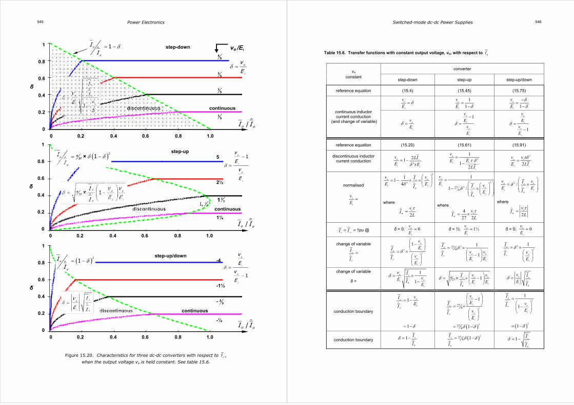
Power Electronics 545
Figure 15.20. Characteristics for three dc-dc converters with respect to oI ,
when the output voltage vo is held constant. See table 15.6.
0 0.2 0.4 0.6 0.8 1.0
1
0.8
0.6
0.4
0.2
0
δ
/o oI I
0 0.2 0.4 0.6 0.8 1.0
1
0.8
0.6
0.4
0.2
0
δ
/o oI I
0 0.2 0.4 0.6 0.8 1.0
1
0.8
0.6
0.4
0.2
0
δ
/o oI I
o
i
v
Eδ =
discontinuous continuous 1
o
o o
oi
i
I
v IvE
E
δ =
−
1o
o
II
δ= − step-down
131,
1o
i
o
i
v
E
v
E
δ
−
=
discontinuous continuous
1o o o
i io
v vIE EI
δ = −
427 ×
step-up
1
o
i
o
i
v
E
v
E
δ =
−
discontinuous continuous
oo
i o
v I
E Iδ =
( )21o
o
II
δ= − step-up/down
( )21o
o
II
δ δ= −427 ×
vo /Ei
45
35
25
15
5
2½
231
1¼ -4
-1½
- 2 3
-¼
Switched-mode dc-dc Power Supplies
546
Table 15.6. Transfer functions with constant output voltage, vo, with respect to Io
converter vo
constant step-down step-up step-up/down
reference equation (15.4) (15.45) (15.75)
o
i
v
Eδ=
1
1o
i
v
E δ=
−
1o
i
v
E
δδ
−=
−
continuous inductor current conduction
(and change of variable) o
i
v
Eδ =
1o
i
o
i
v
Ev
E
δ−
=
1δ =
−
o
i
o
i
v
Ev
E
reference equation (15.20) (15.61) (15.91)
discontinuous inductor current conduction
2
21o i
i i
v LIE Eδ τ
= − 2
1
12
τ δ=
−
o
ii
i
v
EELI
2
2o o
i i
v v
E LI
τδ=
normalised
=o
i
v
E
2
2
11
4o oo
i i
v vIE E
Iδ ∧
= − × ×
o
where
2ov
IL
τ∧
=o
2
2274
1
1 /δ∧
= − ×
o
ioo
i
v
E vIE
I o
where
4
27 2ov
IL
τ∧
= ×o
2 /o oo
i i
v vIE E
Iδ
∧
= × o
where
2
τ∧
= ovI
Lo
∧
= =ooI I 1pu @ δ = 0; 0=o
i
v
E δ = ⅓; 1½=o
i
v
E δ = 0; 0=o
i
v
E
change of variable
∧=o
o
I
I
2
2
1
δ∧
−
= ×
o
io
oo
i
v
EI
vIE
227
41
1
δ∧
= ×
−
o
o oo
i i
I
v vIE E
2
2
1δ∧
= ×
o
oo
i
I
vIE
change of variable
δ =
1
1δ ∧= ×
−
o o
oi
i
v IvE IE
o
427 1δ
∧
= × −
× o oo
i i
v vIE EI o
δ∧
= o o
i
v IE I o
conduction boundary
1
1 δ
∧= −
= −
oo
io
vIE
I
( )
3
2
274
274
1
1δ δ
∧
−
= ×
= −
o
io
oo
i
v
EI
vIE
( )
2
2
1
1
1 δ
∧= −
= −
o
oo
i
I
vIE
conduction boundary 1 oI
Iδ ∧= −
o
( )2274 1oI
Iδ δ
∧= −
o
1 oI
Iδ
∧= −
o

Power Electronics 547
Figure 15.21. Characteristics for three dc-dc converters with respect to iI ,
when the output voltage vo is held constant. See table 15.7.
0 0.2 0.4 0.6 0.8 1.0
1
0.8
0.6
0.4
0.2
0
δ
/i iI I
0 0.2 0.4 0.6 0.8 1.0
1
0.8
0.6
0.4
0.2
0
δ
/i iI I
0 0.2 0.4 0.6 0.8 1.0
1
0.8
0.6
0.4
0.2
0
δ
/i iI I
1,½
o
i
v
Eδ =
discontinuous continuous
½
1
o
i i
oi
i
v
EIvIE
δ = ×−
step-down
1,½
1o
i
o
i
v
E
v
E
δ
−
=
discontinuous continuous
( )4 1i
i
I
Iδ δ= −
½ 1i o
ii
vIEI
δ = × −
step-up
1,½
1
o
i
o
i
v
E
v
E
δ =
−
discontinuous continuous
( )4 1i
i
I
Iδ δ= −
½i
i
o
i
I
I
vE
δ = ×
step-up/down
( )4 1i
i
I
Iδ δ= − vo /Ei
45
35
25
15
5
2½
231
1¼ -4
-1½
- 2 3
-¼
Switched-mode dc-dc Power Supplies
548
Table 15.7. Transfer functions with constant input voltage, vo, with respect to I i
converter vo
constant step-down step-up step-up/down
reference equation (15.4) (15.45) (15.75)
o
i
v
Eδ=
1
1o
i
v
E δ=
−
1o
i
v
E
δδ
−=
−
continuous inductor current conduction
(and change of variable) o
i
v
Eδ =
1o
i
o
i
v
Ev
E
δ−
=
1δ =
−
o
i
o
i
v
Ev
E
reference equation (15.21) (15.60) (15.91)
discontinuous inductor current conduction
2
1
21δ τ
=+
o
i i
o
v
E LI
v
2
12
δ τ= +o o
i i
v v
E LI
2
2
δ τ= −o o
i i
v v
E LI
normalised
=o
i
v
E
where
8
τ∧
= ovI
Li
2
1
11
4δ ∧
=+ ×
o
i i
v
E I
I i
21 4 /δ∧
= +o i
i
v IE
I i
24 /δ∧
= −o i
i
v IE
I i
∧
= =i i
I I 1pu @ δ = ½; ½=o
i
v
E δ = ½; 2=o
i
v
E δ = ½; 1= −o
i
v
E
change of variable
∧=i
i
I
I
2
1
4δ∧
−
= ×
o
ii
oi
i
v
EIv
IE
2 14
1δ
∧= ×
−
i
oi
i
Iv
IE
2 14δ
∧= − ×i
oi
i
Iv
IE
change of variable δ=
all with a boundary
½ ½ 1δ ∧= + − o
o
I
I
½1
δ∧
= ×−
o
ii
o
ii
v
EIv
IE
½ 1δ∧
= × −
oi
ii
vIEI
½δ∧
= × oi
ii
vIEI
conduction boundary
½ ½ 1δ ∧= + − o
o
I
I
( )
4 1
4 1δ δ
∧
= −
= −
o oi
i ii
v vIE E
I
( )
2
1
4
4 1δ δ
∧
−
= ×
= −
o
ii
oi
i
v
EI
vIE
( )
24
1
4 1δ δ
∧= − ×
−
= −
o
ii
oi
i
v
EI
vIE

Power Electronics 549
Figure 15.22. Characteristics for three dc-dc converters, when the input voltage Ei is held constant.
discontinuous
discontinuous
discontinuous
continuous
/i iI I∧
24
o
i
vE
δ−
( )2
4
1
−
−
o
i
o
i
vE
vE
4 1v vo oE Ei i
−
24 1vo
Eivo
Ei
δ −
( )( )2
4 1o
i
o
i
vE
vE
−
1
1o
i
vE δ=
−
o
i
vE
δ=
1o
i
vE
δ
δ
−=
−
2
1
o
i
o
i
vE
vE
δ
−
1o
i
o
i
vE
vE
−
1
1o
i
vE δ=
−
1o
i
vE
δ
δ
−=
−
o
i
vE
δ=( )227
4 1 o
i
vE
δ −
2
/i iI I
δ
∧
=
2
1−
−
o
i
o
i
vE
vE
2
274 1 o o
i i
v vE E
−
/o oI I∧
o
i
vE
24
1o
i
vE
δ
−
δ 2
1
δ = ¾
δ = ¼
δ = ½
δ = ¼
δ = ½
δ = ¼
δ = ½
δ = ½
δ = ¼
δ = ¼
δ = ½
δ = ¾
0
δ = 0
δ = 1
1
δ = 0
δ = 1
δ = ½
δ = ¼
δ = 0 δ = 0
2
-2
-1
1
½
-½
0 1
0
0 0
1
Ei constant Ei constant
Switched-mode dc-dc Power Supplies
550
Figure 15.23. Characteristics for three dc-dc converters, when the output voltage vo is held constant.
/i iI I∧
/ooI I
∧
o
i
vE
o
i
v-E
δ = ¾
δ = ¼
δ = ½
δ = ¼
δ = ½
δ = ¼
δ = ½
δ = ½
δ = ¼
δ = ¼
δ = ½
δ = ¾
0
δ = 0
δ = 1
1
δ = 0
δ = 1
δ = ½
δ = ¼
δ = 0 δ = 0
2
-2
-1
1
½
-½
1
24
o
i
vE
δ−
( )2
4
1
−
−
o
i
o
i
vE
vE
4 1v vo oE Ei i
−
24 1vo
Eivo
Ei
δ −
24
1o
i
vE
δ
−
( )( )2
4 1o
i
o
i
vE
vE
−
1
1o
i
vE δ
=−
o
i
vE
δ=
1o
i
vE
δ
δ
−=
−
( )2
2
o
i
vE
δ−
2 1
2
voEi
voEi
δ −
( )227
4
1o o
i i
v vE E
δ
−
( )3
274 1o
i
o
i
vE
vE
−
1 o
i
vE−
( )2
1
1
−
− o
i
vE
1o
i
vE
δ
δ
−=
−
voEi
δ=
1
1o
i
vE δ=
−
vo constant vo constant
0 0
0 0
discontinuous
discontinuous
continuous
0
0

Pow
er E
lect
ronic
s
551
Tab
le 2
5.8.
C
on
vert
er p
aram
eter
s fo
r d
isco
nti
nu
ou
s an
d c
on
tin
uo
us
ind
uct
or
con
du
ctio
n r
egio
ns
and
bo
un
dar
ies.
Co
nve
rte
r F
orw
ard
step
-dow
n F
lyba
ck
step
-up
Fly
back
st
ep-u
p/d
own
;0
1τ
δτ
=≤
=≤
TtR
kL
dis
continuous
continuous
dis
continuous
continuous
dis
continuous
continuous
()
()
2 1δ
δδ
=
≥×
−crit
ical
o i
k vk
E
21
21
k
kδ
δ
≤−
≥−
21
21
k
kδ
δ
≥−
≤−
(
)2
272
21
δδ
>
−≤
k
k
27
2k≤
()2
21
2
1
δ
δ
≤−
≥−
k
k
()2
21
2
1
δ
δ
≥−
≤−
k
k
()
,δ=
=×
io
o
ii
o
vI
Rk
IE
EI
2
2
8¼
11
δδ
−+
+
k
k
δ
2½
11
2δ
++
k
11
δ−
½
δ−k
1δ δ− −
δτ
=D
D
t
1o i
o iv Ev E
δ−
×
1δ
−
1
1o i
v E
δ×
−
1δ
−
1 o i
v E
δ×
1
δ−
()
1
δτ
δδ
= =−
+
xx
D
t
11
o i
v E
δ−
×
0
1-
1
o i
o iv Ev E
δ×
−
0
1
1
o i
o iv E
v E
δ+
−×
0
,∧
∨
××
LL
ii
RR
II
EE
1
,0δ
−
o i
vk
E
()
½1
o i
vk
Eδ
δ±
−
,0δk
½1
1o i
vk
Eδ
δ×
±−
,0δk
½
11
o i
vk
Eδ
δ×
±−
()
=½
Li
LL
LD
RI
E
Ii
iδ
δ∨×
++
½2
1o i
o iv Ek
v E
δ−
×
o i
v E
½2
1
o i
o iv Ek
v E
δ×
−
11
o i
v Eδ×
−
½2
1o i
o iv Ek
v E
δ+
×
11
o i
v Eδ×
−
/T
tt
Dt
kδ
δτ
<=
½
Tt
tt
δδ
τ<
=∀
T
tt
tδ
τ≤
=
Tt
tt
δτ
≤=
T
tt
tδ
τ≤
=
Tt
tt
δτ
≤=
()
0c L
Do
I it
Iδ
δδ
=
≤≤
+≤
1
Ttt
Dt
kτ
δτ
<≤=
−
()
½1
Ttt
tτ
δ
δτ
<≤
∀ =−
1o
iD T
vE
tk
ttδ
δτ
δ
τ
∀
=−
<≤
()
=½
1-
22
11
2
/T
o i
ot
ti
T
vk
kE
k
vt
Ek
tt
τ
δδ
δ
δτ
τ
<≤
≤−
≥×
−
≤∀ +
<≤
ifth
en
1
o
iD T
vE
tk
ttδ
δτ
δ
τ
∀
=−
<≤
()
=½
1
21
11
11
21
-/
T
o i
ot
ti
Tkk v
kE
vt
Ek
tt
τ
δ
δ
δτ
τ
<≤
≤+
−+
−
≥×
−
+
<≤
Power Electronics
552
ind
ucto
r c
urr
en
tI L
1
0.8
0.6
δ
0.4
0.2
0 0 0.2 0.4 0.6 0.8 1
T D xD x
t t tδ δ δτ τ τ= = =
0 0.2 0.4 0.6 0.8 1
T D xD x
t t tδ δ δτ τ τ= = =
0 0.2 0.4 0.6 0.8 1
Ttδ τ=
0 0.2 0.4 0.6 0.8 1
o
i
vE
1.2
1.0
0.8
0.6
L
L
L
i
i
i∨
0.2
0
δ = 0.15
δ = 0.85
δ = 0.15 δ = 0.85 δ = 0.15
δ = 0.85
time
time
0.85LI =
0.19LI =
Li∨
LI
Li∧
0.49Li∧
=
1.12Li∧
=
0.6Li∨
=
0.85voEi
= 0.19voEi
=
translation
δcrit = ½
0.21
xδ
=
0.64Dδ =
0.64
Dδ
= δ
Figure 15.24. Step-down converter normalised performance monogram for k = 4, giving discontinuous inductor conduction for δcrit ≤ ½. Inductor time domain current waveforms for δcont = 0.85 (continuous inductor current) and δdis = 0.15 (discontinuous inductor current).
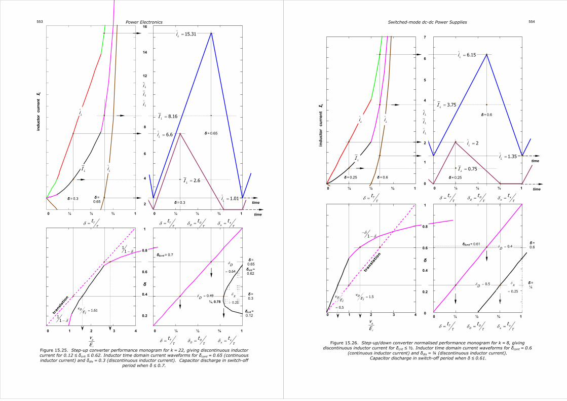
Power Electronics 553
Figure 15.25. Step-up converter performance monogram for k = 22, giving discontinuous inductor current for 0.12 ≤ δcrit ≤ 0.62. Inductor time domain current waveforms for δcont = 0.65 (continuous inductor current) and δdis = 0.3 (discontinuous inductor current). Capacitor discharge in switch-off
period when δ ≤ 0.7.
translation
0 1 2 3 4
o
i
vE
0 ¼ ½ ¾ 1
T D xD x
t t tδ δ δτ τ τ= = =
δ = 0.65
δ = 0.3
1.61voEi
=
1
0.8
0.6
δ
0.4
0.2
δcrit = 0.62
δcrit = 0.12
δIc=0 = 0.7
0.21
xδ
=
0.49Dδ =
ind
ucto
r c
urr
en
tI L
Li∨
Li∧
LI
2.6LI =
8.16LI =
1.01Li∨
=
15.31Li∧
=
6.6Li∧
=
0 ¼ ½ ¾ 1
T D xD x
t t tδ δ δτ τ τ= = =
0 ¼ ½ ¾ 1
Ttδ τ=
16
14
12
L
L
L
i
i
i∨
8
6
4
2
time
time
δ = 0.3 δ = 0.65 δ = 0.3
δ = 0.65
¼, 0.78
0.64
Dδ
=
11 δ−
11 δ−
Switched-mode dc-dc Power Supplies 554
Figure 15.26. Step-up/down converter normalised performance monogram for k = 8, giving discontinuous inductor current for δcrit ≤ ½. Inductor time domain current waveforms for δcont = 0.6
(continuous inductor current) and δdis = ¼ (discontinuous inductor current). Capacitor discharge in switch-off period when δ ≤ 0.61.
0 1 2 3 4
o
i
vE
in
du
cto
r c
urr
en
tI L
Li∨
Li∧
LI
3.75LI =
6.15Li∧
=
1.35Li∨
=
2Li∧
=
7
6
5
4
L
L
L
i
i
i∨
2
1
0 0 ¼ ½ ¾ 1
Ttδ τ=
0 ¼ ½ ¾ 1
T D xD x
t t tδ δ δτ τ τ= = =
time
time
0.75LI =
δ = 0.6 δ = 0.25 δ = 0.25
δ = 0.6
translation
0 ¼ ½ ¾ 1
T D xD x
t t tδ δ δτ τ τ= = =
δ = 0.6
δ = ¼
1.5voEi
=
0.5
voEi
=
1
0.8
0.6
δ
0.4
0.2
0
0.5Dδ = 0.25
xδ
=
0.4Dδ = δIc=0 = 0.61
1δ
δ−
−
Power Electronics
555
Reading list Fisher, M. J., Power Electronics,
PWS-Kent Publishing, 1991. Hart, D.W., Introduction to Power Electronics,
Prentice-Hall, Inc, 1994. Hnatek, E. R., Design of Switch Mode Power Supplies,
Van Nostrand Reinhold, 1981. Mohan, N., Power Electronics, 3rd Edition,
Wiley International, 2003. Thorborg, K., Power Electronics – in theory and practice,
Chartwell-Bratt, 1993. http://www.ipes.ethz.ch/
Problems 15.1. An smps is used to provide a 5V rail at 2.5A. If 100 mV p-p output ripple is allowed and the input
voltage is 12V with 25 per cent tolerance, design a flyback buck-boost converter which has a maximum switching frequency of 50 kHz.
15.2. Derive the following design equations for a flyback boost converter, which operates in the
discontinuous mode.
(max)
(min)(max)
(min)
(min)
(min) (max)
(min)(max)
(min)
(max)
12
1
2
τ
∧
∧
∧∨
∧
= × × = =
− −= = = ×
−
∆∆= = =∆ ∆
constanti
i
i
i
oo D
oi
i
o i o o iT
o io
T o
o o
vi I t
vE fE
v E I v EL t f f
v EIi
i t eQC ESR
e e i
15.3. Derive design equations for the forward non-isolated converter, operating in the continuous
conduction mode. 15.4. Prove that the output rms ripple current for the forward converter in figure 15.2 is given by
/ 2 3oi∆ . 15.5. If the smps inductor has series resistance r, show that the voltage transfer function of the boost
converter, with continuous inductor current, is given by
( )2
1 1
1 11
δδ
= ×− +
−
o
i
vrE
R
where R is the load resistance. Hence show that the power transfer efficiency is
( )2
1
11
η
δ
=+
−r
R
Switched-mode dc-dc Power Supplies 556
15.6. Show that the output voltage of a forward converter is decreased by δvsw+(1-δ)vD when the switch voltage drop is vsw and the diode forward voltage drop is vD.
15.7. In the forward converter example 15.1, the load resistance is varied between 1Ω and 16Ω, over
which range the inductor current becomes discontinuous. With the aid of table 15.2, plot the output voltage as a function of load resistance over the range 1Ω to 16Ω.
15.8. In the step-up converter example 15.2, the load resistance is varied between 2½Ω and 22½Ω,
and the inductor current becomes discontinuous at 22½Ωn. With the aid of table 15.2, plot the output voltage as a function of load resistance over the range 2.5Ω to 45Ω.
15.9. In the step-up converter example 15.3, the load resistance is varied between 2½Ω and 37½Ω,
and the inductor current becomes discontinuous at 37½Ω. With the aid of table 15.2, plot the output voltage as a function of load resistance over the range 2½Ω to 75Ω.
15.10. The forward converter in example 15.1 dissipates 9.216kW. Specify the necessary inductance
change so that the minimum inductor current is 25% of the average inductor current. 15.11. A boost converter has a 12V input voltage and dissipates into a load 960W when the output is
48V. If the inductor ripple current is 50% of the average inductor current, determine the duty cycle and inductance when the switching frequency is 20kHz. If the output voltage ripple is restricted to a maximum of 1%, determine the minimum output capacitance.
15.12. A buck-boost converter has a 12V input voltage and dissipates into a load 960W when the
output is -48V. If the inductor ripple current is 50% of the average inductor current, determine the duty cycle and inductance when the switching frequency is 20kHz. If the output voltage ripple is restricted to a maximum of 1%, determine the minimum output capacitance.
15.13. The isolated flyback converter in figure 15.11c has an input voltage of 50V, an output of 25V, an
on-state duty cycle ratio of 0.4, and a 20kHz switching frequency. If the load is a 5Ω resistor, determine
i. the transformer turns ratio ii. the core self inductance such that the ripple current is half its average current.
15.14. The isolated forward converter in figure 15.11a has the following specification: Ei = 96V,
N1:N2:N3 = 1 with 4mH self inductance, filter inductance 250µH, load resistance 24Ω, onstate duty cycle = 0.4 and a 40kHz switching frequency. Determine
i. the output voltage and output ripple voltage if C=220µF ii. average and p-p current in the 250 µH output inductor iii. the peak magnetising current in the model self inductance iv. peak switching current.
15.15. The push-pull converter in figure 15.5a has the following specification: Ei = 96V, Np:Np:Ns = 1:1:2
with 500µH of output inductance with respect to the primary, 12Ω load resistance, and a 25kHz switching frequency. For an on-state duty cycle of determine
i. the output voltage ii. the average and p-p output-inductance current iii. the output voltage ripple across a 470µF output capacitor.
Sketch the switch, diode, source and capacitors currents, using the inductor current as reference.
15.16. Repeat problem 15.15 if the core magnetising inductance (self-inductance) is 2.5mH with
respect to the primaries. Having determined the peak magnetising current, add the magnetising inductance current waveform to the other sketched waveforms.
15.17 A forward converter operates at 50kHz with a 60% duty cycle from a 15V dc supply and
delivers 27W into a resistive load. Determine the output voltage and inductor rms current. Sketch the capacitor and inductor current and voltage waveforms. What output capacitance will result in 1% output voltage ripple? What inductance will ensure continuous conduction at 3W output?