chapter 2 basic concepts of electronics. figure 2.1 electric current within a conductor. (a) random...
TRANSCRIPT
Chapter 2
Basic Concepts of ElectronicsBasic Concepts of Electronics

E lectron
I
+
+-
-
+
-
Figure 2.1 Electric current within a conductor. (a) Random movement of electrons generates no current. (b) A net flow of electrons generated by an external force.
(a) (b)

I
EV b V a
l
Figure 2.2 A model of a straight wire of length l and cross-sectional area A. A potential difference of Vb – Va is maintained across the conductor, setting up an electric field E. This
electric field produces a current that is proportional to the potential difference.

F irs t d ig it (A )
Second d ig it (B )
M ultip lie r (C )
T olerance (D )
Figure 2.3 The colored bands that are found on a resistor can be used to determine its resistance. The first and second bands of the resistor give the first two digits of the resistance, and the third band is the multiplier which represents the power of ten of the resistance value. The final band indicates what tolerance value (in %) the resistor possesses. The resistance value written in equation form is AB10C D%.

Table 2.1 The color code for resistors. Each color can indicate a first or second digit, a multiplier, or, in a few cases, a tolerance value.
ColorColor NumberNumber Tolerance (%)Tolerance (%)
BlackBlack 00
BrownBrown 11
RedRed 22
OrangeOrange 33
YellowYellow 44
GreenGreen 55
BlueBlue 66
VioletViolet 77
GrayGray 88
WhiteWhite 99
GoldGold ––11 5%5%
SilverSilver ––22 10%10%
ColorlessColorless 20%20%

I R
+ -V
(a)
V 1 V 2
+ -10 W
I
+ -20 W
V S = 30 V
R 1 R 2
(b)
Figure 2.4 (a) The voltage drop created by an element has the polarity of + to – in the direction of current flow. (b) Kirchhoff’s voltage law.
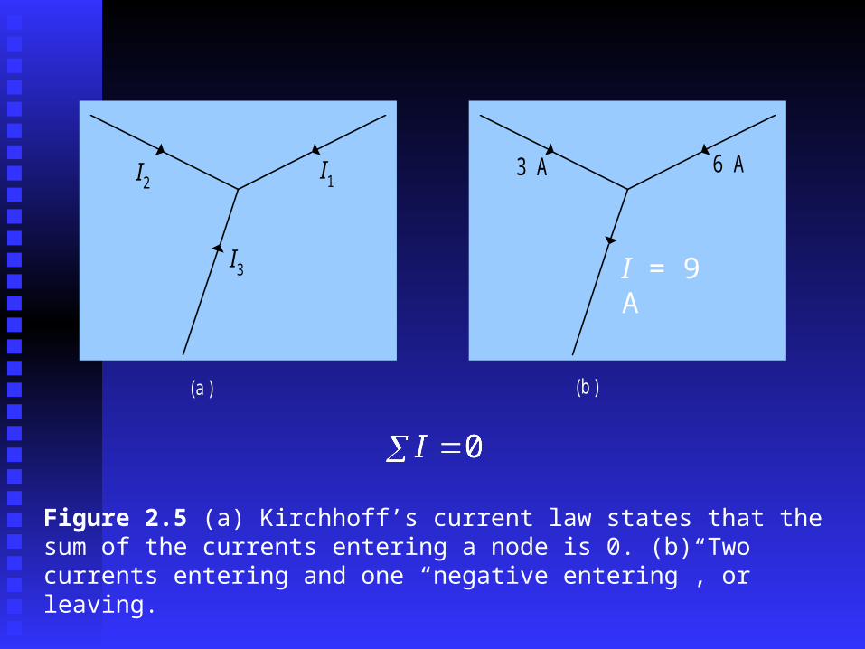
I1I2
I3
3 A
I = ?
(a ) (b )
6 A
Figure 2.5 (a) Kirchhoff’s current law states that the sum of the currents entering a node is 0. (b) Two currents entering and one “negative entering”, or leaving.
I = 9 A

+
-10 V
I1
2 W6 W
4 W
I3 I2
-
+14 V
a b e
d c f
Figure 2.6 Kirchhoff’s current law example.

+ -20 W + -20 W
20 V30 V
A BC
20 W-
+
-
+
-
+V
Figure 2.7 Example of nodal analysis.

100 kW
1 MW
1 m VR s
R i
V o
E lectrocard iogram
Figure 2.8 The 1 mV signal from the electrocardiogram is attenuated by the resistive divider formed by the 100 kW skin resistance and the 1 MW input resistance of the oscilloscope.

Figure 2.9 A potentiometer is a three-terminal resistor with an adjustable sliding contact shown by the arrow. The input signal vi is attenuated by the potentiometer to yield an adjustable smaller voltage vo.
v i
vo
Slider

R p
G alvanom eter
R s
G alvanom eter
(a) (b)
Figure 2.10 (a) When a shunt resistor, Rp, is placed in parallel with a galvanometer, the device can be used as an ammeter. (b) When a resistor, Rs, is connected in series with the galvanometer, it can be used as a voltmeter.

R 1 R 1
R 3 R x
a b
+
-
I1 I2
Figure 2.11 A circuit diagram for a Wheatstone bridge. The circuit is often used to measure an unknown resistance Rx, when the three other resistances are known.
When the bridge is balanced, no current passes from node a to node b.

dv/dt
i
1
C +
-
Cv
i
(a ) (b )
Figure 2.12 (a) Capacitor current changes as the derivative of the voltage (b) Symbol of the capacitor.

+Q- Q
d Area = A
Figure 2.13 Diagram of a parallel plate capacitor. The component consists of two parallel plates of area A separated by a distance d. When charged, the plates carry equal charges of opposite sign.

C 1 C 2
(a)
Figure 2.14 (a) A series combination of two capacitors. (b) A parallel combination of two capacitors.
C 1
C 2
(b)

di/dt
V
1
L +
-
Lv
i
(a ) (b )
Figure 2.15 (a) Inductor voltage changes as the derivative of the current. (b) Symbol of the inductor.
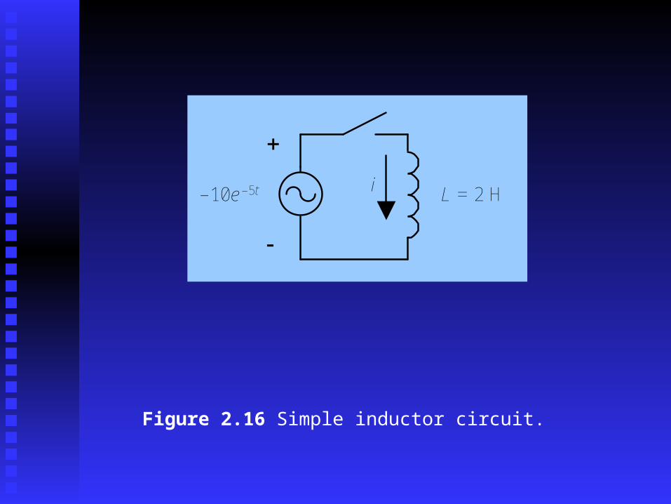
Figure 2.16 Simple inductor circuit.
+
-
L = 2 H–10e–5t i

R
iR
+
-iC
+
-
C
Figure 2.17 (a) Simple RC circuit with v (0) on capacitor at time t = 0. (b) Normalized voltage across the capacitor for t 0 (normalized means the largest value is 1).
(a)
V C (0 )1
t t
V C (t)
(b)

+ -vR
vCV
I
-
+
-
+
(a)
Figure 2.18 (a) Series RC circuit with voltage step input at time 0. (b) Normalized voltage across the capacitor.
1
t t
V C (t)
V C (t)
V
(b)

Figure 2.19 Plot of vo for Example 2.8
12
0.023 0.05
v C (
V)
Time (s)
10.8

1
0A
mpl
itude
tT
sine
cosine- 1
Figure 2.20 One period, T, of the sine and cosine waveforms.
A = amplitude of sine wave
f = frequency of sine wave in hertz (Hz)
= phase angle of sine wave in radians
= angular frequency of sine wave in radians per second
T = 1/f (period in seconds)

0 1 2 3 4 5 6–1
–0 .5
0
0 .5
1
t (s)
v (V
)
Figure 2.21 Sinusoidal waveforms with different frequencies.
)sin( ty )2sin( ty
)sin( - ty
0 1 2 3 4 5 6–1
–0 .5
0
0 .5
1
t (s)
v (V
)
)sin( ty
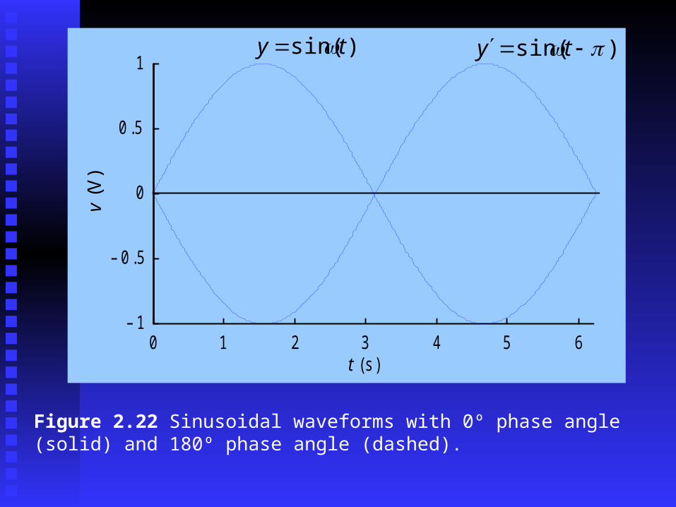
Figure 2.22 Sinusoidal waveforms with 0º phase angle (solid) and 180º phase angle (dashed).
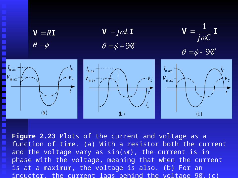
t
Im ax
V m ax
iR
vR
(a)
Figure 2.23 Plots of the current and voltage as a function of time. (a) With a resistor both the current and the voltage vary as sin(t), the current is in phase with the voltage, meaning that when the current is at a maximum, the voltage is also. (b) For an inductor, the current lags behind the voltage 90. (c) For a capacitor, the current lead the voltage by 90.
t
Im ax
V m ax
iL
vL
(b)
t
Im ax
V m ax
iC
vC
(c)

Z e
(c)
Z 1
Z 2
(a)
Z 1Z 2
(b)
Figure 2.24 (a) Series circuit. (b) Parallel circuit. (c) Single impedance equivalent.
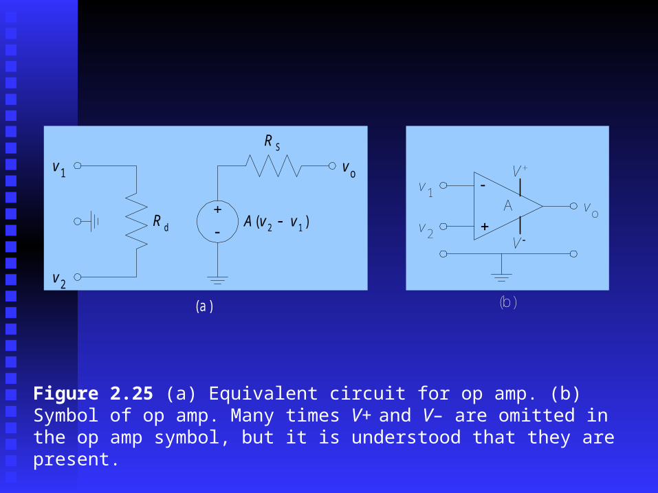
R d
R S
+
A (v2 - v1)
v1
v2
vo
-
(a)
vo
v1
v2
A-
+
(b)
V+
V-
Figure 2.25 (a) Equivalent circuit for op amp. (b) Symbol of op amp. Many times V+ and V– are omitted in the op amp symbol, but it is understood that they are present.

vo
v i
R i
ii
R f
A-
+
Figure 2.26 An inverting amplifier. The gain of the circuit is –Rf/Ri
From Ohm’s law:

Figure 2.27 Inverter circuit attached to a generator that contains an internal resistance.
vo
vi
R i
R f
A
-
+vs= 1 V
Rs

R f
vov i
R i
ii
A-
+
(a)
vov i
-
+
(b)
Figure 2.28 (a) A noninverting amplifier, which also depends on the ratio of the two resistors. (b) A follower, or buffer, with unity gain.

vo
R f
A
-
+
vs= 1 V
Rs
R i
vi
Figure 2.29 The gain of the noninverting amplifier is not affected by the addition of the impedance Rs due to the generator.
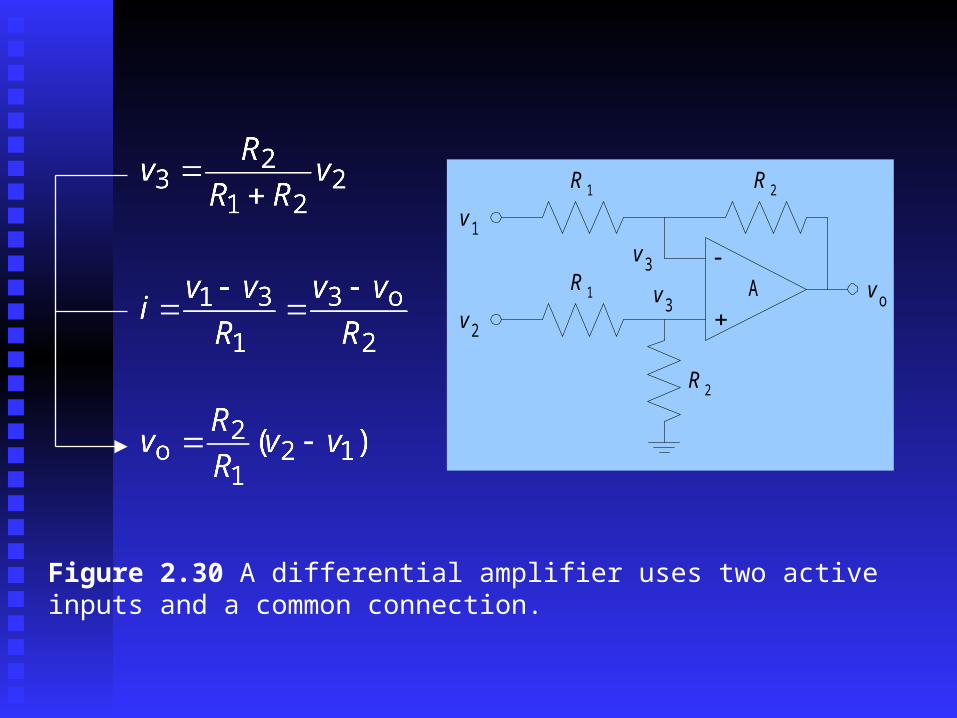
R 2
vo
v1
R 1
R 1
R 2
v2
v3
v3A
-
+
Figure 2.30 A differential amplifier uses two active inputs and a common connection.

R2
vo
R1
R1
R2
A
-
+
-
+
-
+
Rs
Rs
/2vd
+
_
/2vd
+
_
vc
+
_
Figure 2.31 Differential amplifier attached to a common mode voltage that contains varying impedances. Adding buffers ensure that fluctuations in Rs does not affect the gain.

R 5 =1 .5 kW
vo
4 V
R 4 = 1 kW
R 1 = 1 kW
R 3 = 1 kW
8 V
v3
v3A
-
+
R 2 = 500 W
I
Figure 2.32 Differential amplifier for Example 2.13.
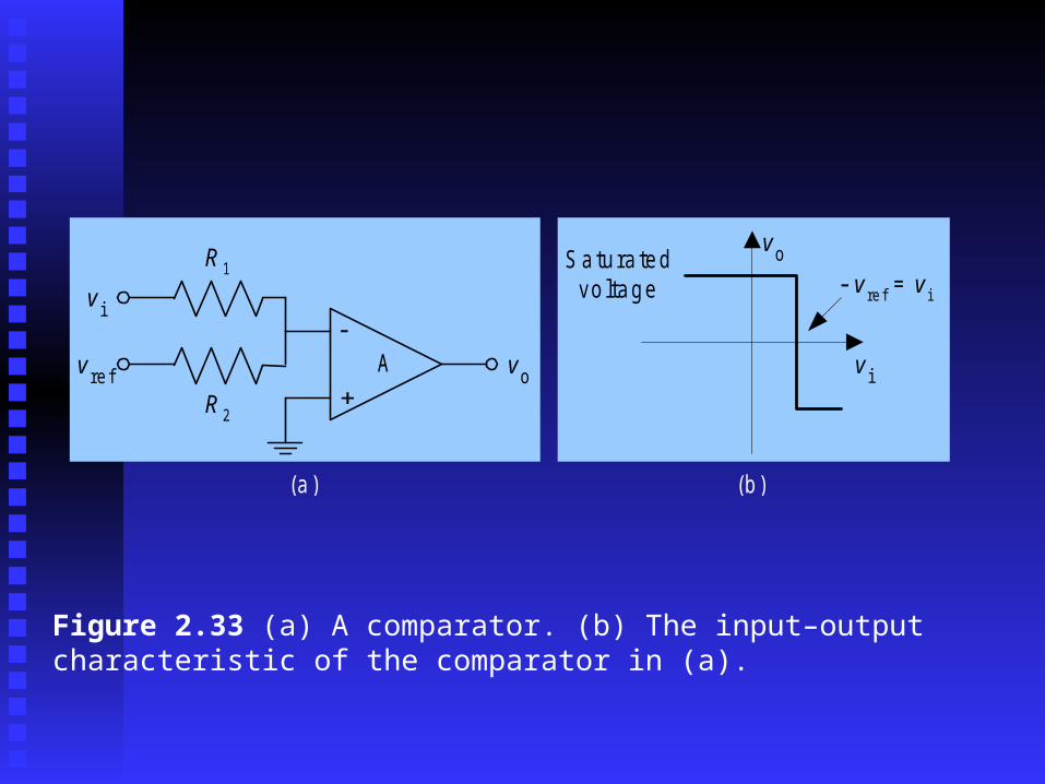
vo
v i
R 1
R 2
v re fA
-
+
(a)
vo
v i
S atu ra tedvo ltage - v re f = v i
(b)
Figure 2.33 (a) A comparator. (b) The input–output characteristic of the comparator in (a).

Figure 2.34 Heart beat detector uses a comparator to determine when the R wave exceeds a threshold.
P
Q
R
S
T
Threshold

Gai
n
F requency (H z)
100 104102 1061
10 C ircu it ga in o f 10
Figure 2.35 The typical op amp open loop gain is much larger, but less constant, than the circuit gain. However the in circuit bandwidth is larger than the open loop bandwidth.
C ircu it bandw id thIdea lga in
Typ ica l openloop ga in

(a) (b)
Figure 2.36 (a) Low-pass filter. (b) High-pass filter.
T(f)
ffc
1.0
0.1
0.01
1 10010
PB
T(f)
ffc
1.0
0.1
0.01
1 10010
PB

(c) (d)
Figure 2.36 (c) Bandpass filter. (d) Bandstop filter. (PB denotes passband)
T(f)
ff2f1
1.0
0.1
0.01
1 10010
PB
T(f)
ff1 f2
1.0
0.1
0.01
1 10010
PBPB

(a)
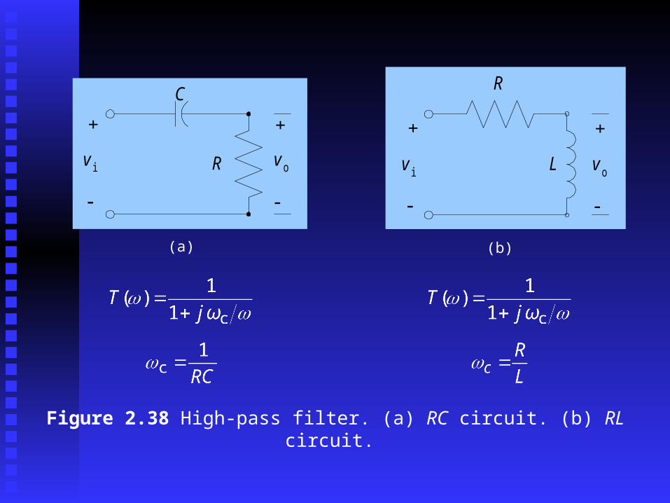
Figure 2.37 Low-pass filter. (a) RC circuit. (b) RL circuit.
R
vo
+
-
v i C
+
-
(b)
R vov i
L+
-
+
-
(a)
Figure 2.38 High-pass filter. (a) RC circuit. (b) RL circuit.
R vov i
C
+
-
+
-
(b)
R
vov i L
+
-
+
-

Low -pass filte rco rner frequency
2
H igh-pass filte rco rner frequency
1
Inpu t s igna l O utpu t
Figure 2.39 A low-pass filter and a high-pass filter are cascaded to make a bandpass filter.

Figure 2.40 A square wave of period T oscillates between two values.
T
Th Tl

Figure 2.41 The 555 timer (a) Pinout for the 555 timer IC. (b) A popular circuit that utilizes a 555 timer and four external components creates a square wave with duty cycle > 50%. (c) The output from the 555 timer circuit shown in (b).
1
2
3
4 5
6
7
Ground
555
Trigger
Output
Reset
8
Control
Threshold
Discharge
Vcc
8 4
+5V
Ra
Rb
7
C
6
251
3
Th = -ln(0.5)(Ra+Rb)C
5 V
0 V
Tl = -ln(0.5)RbC
(a)
(c)
(b)
An
alo
g o
utp
ut
000 100011010001 111110101
1/8 V ref
0 V
7/8 V ref
6/8 V ref
5/8 V ref
4/8 V ref
3/8 V ref
2/8 V ref
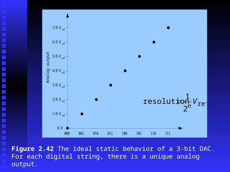
Figure 2.42 The ideal static behavior of a 3-bit DAC. For each digital string, there is a unique analog output.
ref2
1resolution V
n

3-to 8 decoderV re f
R
R
R
R
R
R
R
R
7 6 5 4
b2 b1 b0
V o
3 2 1 0
Figure 2.43 A 3-bit voltage scaling DAC converter.

Dig
ital o
utpu
t
000
100
011
010
001
111
110
101
1/80 /8 7 /86 /85 /84 /83 /82 /8 V re f
Figure 2.44 Converting characteristic of 3-bit ADC converter.

C lockD ig ita lcon tro l
log ic+
_
V in
D ig ita lou tpu t
C lock
D A C converte r
Figure 2.45 Block diagram of a typical successive approximation ADC.

C onvers ion cycle
000
100011010001
111110101
10 32
1/2 V re f
4
V o u t
001
011
101
111110
010
100
Figure 2.46 The possible conversion paths of a 3-bit successive approximation ADC.

0 3 54 621- 1
1
0A
mpl
itude
T im e
(a)
0 15 2520 30105- 1
1
0
Am
plitu
de
S am p lenum bers
)(][ a nTxnx
(b)
Figure 2.47 (a) Continuous signal. (b) Sampled sequence of the signal in (a) with a sampling period of 0.2 s.

Ma
gnitu
de
F requencyfS 2fS
S am plingfunction(b)
Ma
gnitu
de
F requencyfC
O rig ina l
Figure 2.48 (a) Spectrum of original signal. (b) Spectrum of sampling function. (c) Spectrum of sampled signal. (d) Low-pass filter for reconstruction. (e) Reconstructed signal, which is the same as the original signal.
(a)
fS
Mag
nitu
de
F requencyfC 2 fSfS- fC
S am pledsigna l(c)
Mag
nitu
de
F requencyfn
Low -passfilte r(d)
Mag
nitu
de
F requencyfC
R econstructedsigna l(e)
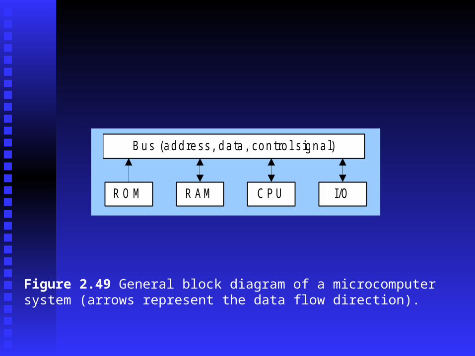
B us (address, da ta , con tro l s igna l)
R O M I/OC P UR A M
Figure 2.49 General block diagram of a microcomputer system (arrows represent the data flow direction).

CPU
Operating System
Editor Complier Linker
Application software
Problem
Figure 2.50 Three levels of software separate the hardware of microcomputer from the real problem.

Deflectioncontrol
Cathode
Screen
Figure 2.51 Sketch for cathode ray tube (CRT). There are two pairs of electrodes to control the deflection of the electron, but only one pair is shown.