chapter 2 matrix converter fundamentalsshodhganga.inflibnet.ac.in/bitstream/10603/17547/... ·...
TRANSCRIPT

13
CHAPTER 2
MATRIX CONVERTER FUNDAMENTALS
In industrial applications there is a strong demand for power quality and energy
efficient power converters with reduced number of switches. MC has recently
received considerable interests, because it possesses the necessary features to fulfil
these current trends. The most desirable features of MC in power converters are
a. Generation of output voltage with the desired amplitude and frequency
b. Sinusoidal input current
c. Sinusoidal output voltage
d. Improved power factor
e. Regeneration Capability
These features of MC replace Voltage Source Inverters in IM drive applications. MC
uses nine bi-directional controlled switches in a 3 x 3 matrix form to produce variable
output voltage with variable frequency. The main advantage of MC is that it does not
have any dc link and energy storing elements which reduce the performance of the
converter.
2.1 Circuit Topologies
Various MC topologies have been studied since 1970 [11]. In 1980, Venturini and
Alesina presented the power circuit of the MC as a matrix of bi-directional power
switches and they introduced the name “MC” [12-13]. The circuit topology of Direct
MC shown in Fig. 2.1 and Indirect MC shown in Fig.2.2 has been studied since 1993.
[14-19].

14
Fig. 2.1: Direct MC
Fig. 2.2: Indirect MC
In the beginning, power transistors were used as bi-directional switches in MC
topology [20-24]. The performance of Direct MC and Indirect MC based on SVM in
an IM drive is also compared [16]. It is shown that the output voltage of the

15 converters does not follow the input. This is due to the need of different commutation
methods to provide safe operation and also the power losses caused by different main
circuits. Also, the effect of non-linearity is more visible in Indirect MC than in Direct
MC. Hence the efficiency of Indirect MC is low compared to Direct MC [16].
In 2001, a new circuit topology of MC called Sparse Matrix Converter (SMC) shown
in Fig.2.3 was invented. The reduced number of components, less complexity in
modulation algorithm and no multistep commutation procedure of SMC attracts its
application in AC drives in Industrial operations. SMC is constructed with 15
transistors, 18 diodes and 7 isolated Driver Potentials [25-27]. The SMC provides
identical function like Direct MC with reduced number of switches. The improved
DC link current commutation scheme reduces the control complexity and increases
the safety and reliability with limitations in functionality. The modified SVM called
Very Sparse Matrix Converter (VSMC) topology shown in Fig. 2.4 consists of 12
transistors, 30 diodes and 10 isolated driver potentials. The limitations in functionality
of SMC are avoided in VSMC and also the number of transistors is reduced in VSMC
compared to SMC whereas the conduction loss is increased due to increase in number
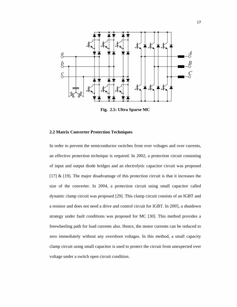
of conducting diodes. The Ultra Sparse Matrix Converter (USMC) shown in Fig. 2.5
was developed with 9 transistors, 18 diodes and 7 isolated driver potentials to reduce
the conduction loss. But the maximum displacement angle between input voltage and
input current is limited to ±30°. In the year 2009, the Z source MC was proposed. It
comprises voltage fed structure and current fed structure. It overcomes the voltage
transfer limitations of MC [28].

16
Fig. 2.3: Bidirectional Sparse MC
Fig. 2.4: Very Sparse MC
17
Fig. 2.5: Ultra Sparse MC
2.2 Matrix Converter Protection Techniques
In order to prevent the semiconductor switches from over voltages and over currents,
an effective protection technique is required. In 2002, a protection circuit consisting
of input and output diode bridges and an electrolytic capacitor circuit was proposed
[17] & [19]. The major disadvantage of this protection circuit is that it increases the
size of the converter. In 2004, a protection circuit using small capacitor called
dynamic clamp circuit was proposed [29]. This clamp circuit consists of an IGBT and
a resistor and does not need a drive and control circuit for IGBT. In 2005, a shutdown
strategy under fault conditions was proposed for MC [30]. This method provides a
freewheeling path for load currents also. Hence, the motor currents can be reduced to
zero immediately without any overshoot voltages. In this method, a small capacity
clamp circuit using small capacitor is used to protect the circuit from unexpected over
voltage under a switch open circuit condition.

18 2.3 Current Commutation Methods in MC
The MC uses bidirectional controlled switches in matrix form. Due to the absence of
freewheeling path, the commutation of switches is the major problem in MC. In order
to transfer current safely from one bidirectional switch to the other, timing and
synchronization of the switch command signals must be chosen carefully.
In order to achieve safe commutation of switches, minimization of commutation time
was proposed in 2004 [26]. Another commutation method for reducing the losses
caused by the reverse leakage current was proposed in 2005 [31]. In this method the
output current direction and voltage polarities of bidirectional switches were used to
perform a two-step commutation.
2.4 Modulation Methods
The objective of MC modulation strategy is to obtain the target sinusoidal output
voltages and sinusoidal input currents with controllable input power factor. The
conditions of the switches are such that output circuit should never be open circuited
and any two input phases should not be short circuited.
Alesina and Venturini [32-33] introduced the “low frequency matrix” concept. They
developed a mathematical analysis which describes the low frequency behaviour of
the converter. The modulation method introduced is called direct transfer function
approach, in which the output voltages are obtained by the multiplication of the
modulation matrix with input voltages [34]. In this method, the output phase voltages
are formed separately and are between negative and positive envelopes of the input
voltage as shown in Fig.2.6. The maximum voltage transfer ratio achieved by this
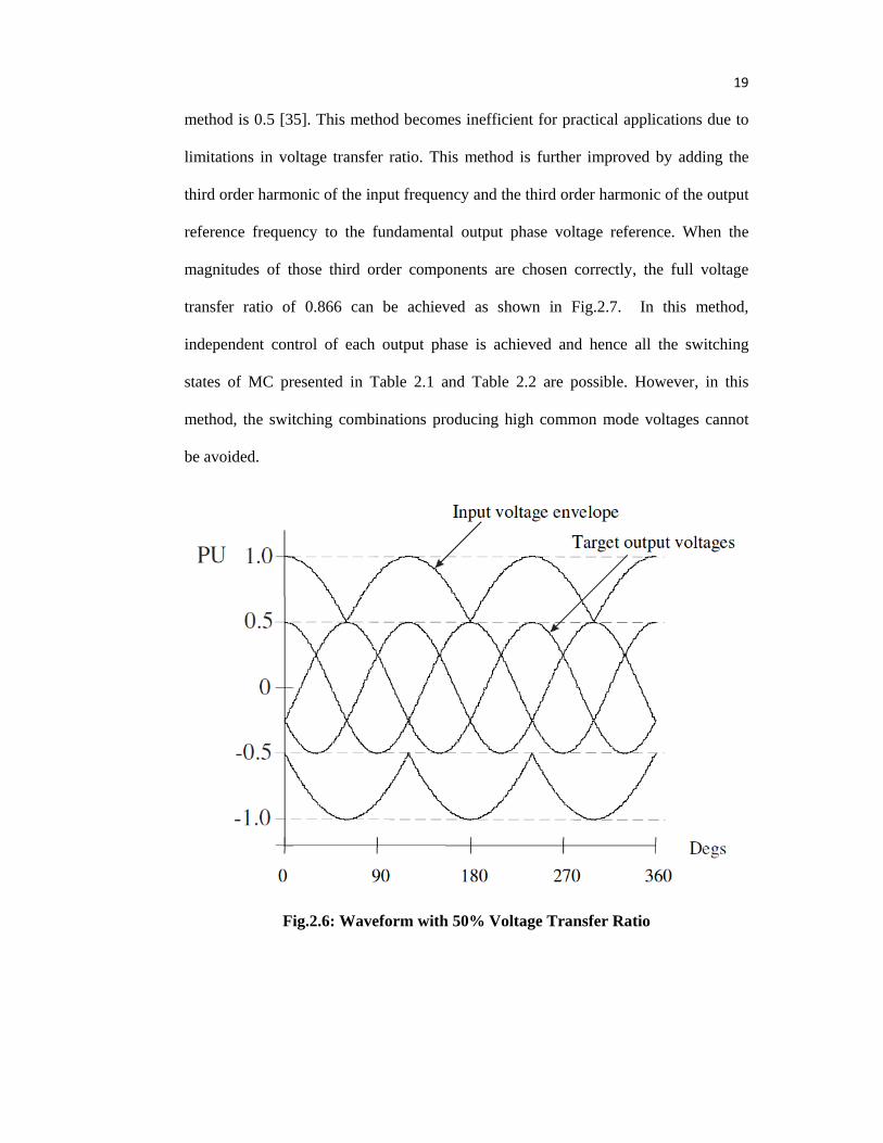
19 method is 0.5 [35]. This method becomes inefficient for practical applications due to
limitations in voltage transfer ratio. This method is further improved by adding the
third order harmonic of the input frequency and the third order harmonic of the output
reference frequency to the fundamental output phase voltage reference. When the
magnitudes of those third order components are chosen correctly, the full voltage
transfer ratio of 0.866 can be achieved as shown in Fig.2.7. In this method,
independent control of each output phase is achieved and hence all the switching
states of MC presented in Table 2.1 and Table 2.2 are possible. However, in this
method, the switching combinations producing high common mode voltages cannot
be avoided.
Fig.2.6: Waveform with 50% Voltage Transfer Ratio

20
Fig.2.7 Third Order Harmonic Injection to Achieve Voltage
Transfer Ratio of 86.6% [36]
In 1983, Rodrigues [37] introduced a switching method using PWM technique in
which each output line switches between the most positive and most negative input
lines. This method is called “fictitious DC link” method. This concept is also known
as “indirect transfer function approach”. In 1985, the use of Space Vectors in the
analysis and control of MCs was introduced by Kastner and Rodriguez [30]. In 1987,
G. Roy presented a scalar control algorithm for MC. In this method voltage transfer
ratio of 0.866 was achieved as in Venturini method. The only difference between the
Venturini method and Scalar Control method is that in Scalar control method, the
voltage transfer ratio is fixed at its maximum value and its effect on output voltage is
negligible in high frequency applications. In 2009, Bachir and Bendiabedellah [39]
presented a detailed comparative study between Venturini and Roy modulation

21 methods. The study result shows the performance of IM for various speed and torque
references. During 1989 - 1995, the principles of Space Vector Modulation (SVM)
and their applications in MC were published by Huber [31-36]. Many researchers
focus on SVM method [46]. SVM method uses simpler algorithms compared to
Venturini method. It is used to calculate the duty cycles of the active voltage vector in
each switching cycle period. This method is capable of controlling the input current,
output voltage and input power factor. The SVM Algorithm derived from indirect
transfer approach is proposed to increase the rms output voltage [47].
Table2.1 Switching Configuration
Group State Phase Switching function values
A B C SAa SAb SAc SBa SBb SBc SCa SCb SCc
I
1 A B c 1 0 0 0 1 0 0 0 12 A C b 1 0 0 0 0 1 0 1 03 B A c 0 1 0 1 0 0 0 0 14 B C a 0 1 0 0 0 1 1 0 05 C A b 0 0 1 1 0 0 0 1 06 C B a 0 0 1 0 1 0 1 0 0
IIA
1 A C c 1 0 0 0 0 1 0 0 12 B C c 0 1 0 0 0 1 0 0 13 B A a 0 1 0 1 0 0 1 0 04 C A a 0 0 1 1 0 0 1 0 05 C B b 0 0 1 0 1 0 0 1 06 A B b 1 0 0 0 1 0 0 1 0
IIB
1 C A c 0 0 1 1 0 0 0 0 12 C B c 0 0 1 0 1 0 0 0 13 A B a 1 0 0 0 1 0 1 0 04 A C a 1 0 0 0 0 1 1 0 05 B C b 0 1 0 0 0 1 0 1 06 B A b 0 1 0 1 0 0 0 1 0
IIC
1 C C a 0 0 1 0 0 1 1 0 02 C C b 0 0 1 0 0 1 0 1 03 A A b 1 0 0 1 0 0 0 1 04 A A c 1 0 0 1 0 0 0 0 15 B B c 0 1 0 0 1 0 0 0 16 B B a 0 1 0 0 1 0 1 0 0
III 1 A A a 1 0 0 1 0 0 1 0 02 B B b 0 1 0 0 1 0 0 1 03 C C c 0 0 1 0 0 1 0 0 1

22
Table2.2 MC Switching State Selection
S.No. Switching Configuration
Converter State
Output voltage
(v0)
Output Voltage Vector
Angle (α0)
Input Current
(ii)
Input Current Vector
Angle (βi)
1 +1 Sabb vab 0 2
√3 -
2 -1 Sbaa - vab 0 2
√3 -
3 +2 Sbcc vbc 0 2
√3
2
4 -2 Scbb - vbc 0 2
√3
2
5 +3 Scaa vca 0 2
√3 7
6
6 -3 Sacc - vca 0 2
√3 7
6
7 +4 Sbab vab 23
2√3
-
8 -4 Saba - vab 23
2√3
-
9 +5 Scbc vbc 23 2
√3
2
10 -5 Sbcb - vbc 23
2√3
2
11 +6 Saca vca 23
2√3
76
12 -6 Scac - vca 23
2√3
76
13 +7 Sbba vab 43 2
√3 -
14 -7 Saab - vab 43
2√3
-
15 +8 Sccb vbc 43 2
√3
2
16 -8 Sbbc - vbc 43 2
√3
2
17 +9 Saac vca 43 2
√3 7
6
18 -9 Scca - vca 43 2
√3 7
6
19 0a Saaa 0 - 0 0
20 0b Sbbb 0 - 0 0
21 0c Sccc 0 - 0 0
22 FRa Sabc - - - -
23 FRb Sacb - - - -
24 FRc Sbca - - - -
25 BRa Sbac - - - -
26 BRb Scab - - - -
27 BRc Scba - - - -

23
2.4.1 Venturini Algorithm
Various modulation techniques can be applied to MC to achieve sinusoidal input
current and output voltage with minimised harmonic distortion and power loss. Also
the modulation technique should follow two important rules. The MCs are fed by
Voltage sources. Hence the input phases should not be short circuited. The load is of
inductive nature so the output phases should never be open-circuited. The modulation
control strategy satisfying the above conditions was first proposed by Alesina and
Venturini and is called Venturini Algorithm.
In MC each switch is used to connect or disconnect any phase of the input to any
phase of the load. This can be achieved only by selecting proper switching
configuration. In order to avoid the interruption of load current suddenly, at least one
switch in each column must be closed. Each switch can be defined with a
commutation function described as below:
0 1 (2.1)
where , , is input phase and k , , is output phase. The two
conditions in equation (2.1) can be expressed as
1 (2.2)
The equation (2.2) shows that a 3 x 3 MC has got 27 possible switching states. In
order to select appropriate combinations of open and closed switches and to generate
the desired output voltages, modulation strategy for the MC must be developed for
which it is necessary to develop the mathematical model. It can be derived from
equation (2.1) as follows:
The load and source voltages with reference to supply neutral can be expressed as

24
and (2.3)
The load and source currents can expressed as
and (2.4)
(2.5)
(2.6)
(2.7)
where K represents input phases A,B,C and k represents output phases a, b, c and Ts
is the sequence time.
The modulation strategies are defined by using these continuous time functions.
(2.8)
(2.9)
Voltages , & and currents , & are average values of output voltage and
outupt current respectively.
The MC generates sinusoidal output voltage and sinusoidal input current to get
adjustable input power factor. Hence, the output voltage can be expressed as
cos cos
cos (2.10)
25
cos cos
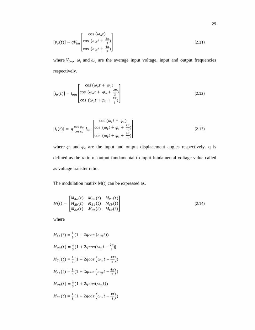
cos (2.11)
where , and are the average input voltage, input and output frequencies
respectively.
cos cos
cos (2.12)
cos cos
cos (2.13)
where and are the input and output displacement angles respectively. q is
defined as the ratio of output fundamental to input fundamental voltage value called
as voltage transfer ratio.
The modulation matrix M(t) can be expressed as,
(2.14)
where
1 2
1 2 ))
1 2
1 2
1 2
1 2

26
1 2
1 2
1 2
where is the modulation frequency.
Hence,
(2.15)
(2.16)
The MC equation can be written as
∑ , , ∑ ,, , ∑ , , 1 (2.17)
Venturini provided two solutions for the problem one with and
another with and are expressed as and respectively
as given below
1 2 cos 1 2 cos 1 2 cos
1 2 cos 1 2 cos 1 2 cos
1 2 cos 1 2 cos 1 2 cos
(2.18)
1 2 cos 1 2 cos 1 2 cos
1 2 cos 1 2 cos 1 2 cos
1 2 cos 1 2 cos 1 2 cos
(2.19)
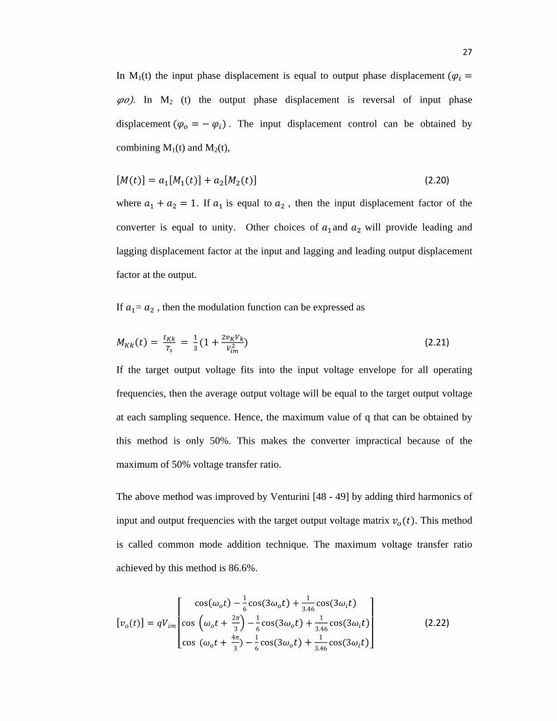
27 In M1(t) the input phase displacement is equal to output phase displacement
. In M2 (t) the output phase displacement is reversal of input phase
displacement . The input displacement control can be obtained by
combining M1(t) and M2(t),
(2.20)
where 1. If is equal to , then the input displacement factor of the
converter is equal to unity. Other choices of and will provide leading and
lagging displacement factor at the input and lagging and leading output displacement
factor at the output.
If = , then the modulation function can be expressed as
1 (2.21)
If the target output voltage fits into the input voltage envelope for all operating
frequencies, then the average output voltage will be equal to the target output voltage
at each sampling sequence. Hence, the maximum value of q that can be obtained by
this method is only 50%. This makes the converter impractical because of the
maximum of 50% voltage transfer ratio.
The above method was improved by Venturini [48 - 49] by adding third harmonics of
input and output frequencies with the target output voltage matrix . This method
is called common mode addition technique. The maximum voltage transfer ratio
achieved by this method is 86.6%.
cos 16
cos 3 13.46
cos 3
cos 23
16
cos 3 13.46
cos 3
cos 43
16
cos 3 13.46
cos 3
(2.22)
28 For unity displacement factor, the modulation factor becomes,
1.
sin sin 3 (2.23)
where 0, , and K represents the input phases A, B, C.
If the displacement factor is other than unity, then the output voltage limit will be
reduced from 0.86Vim to smaller value.
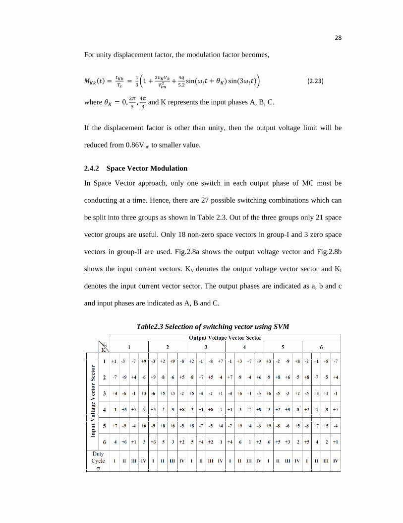
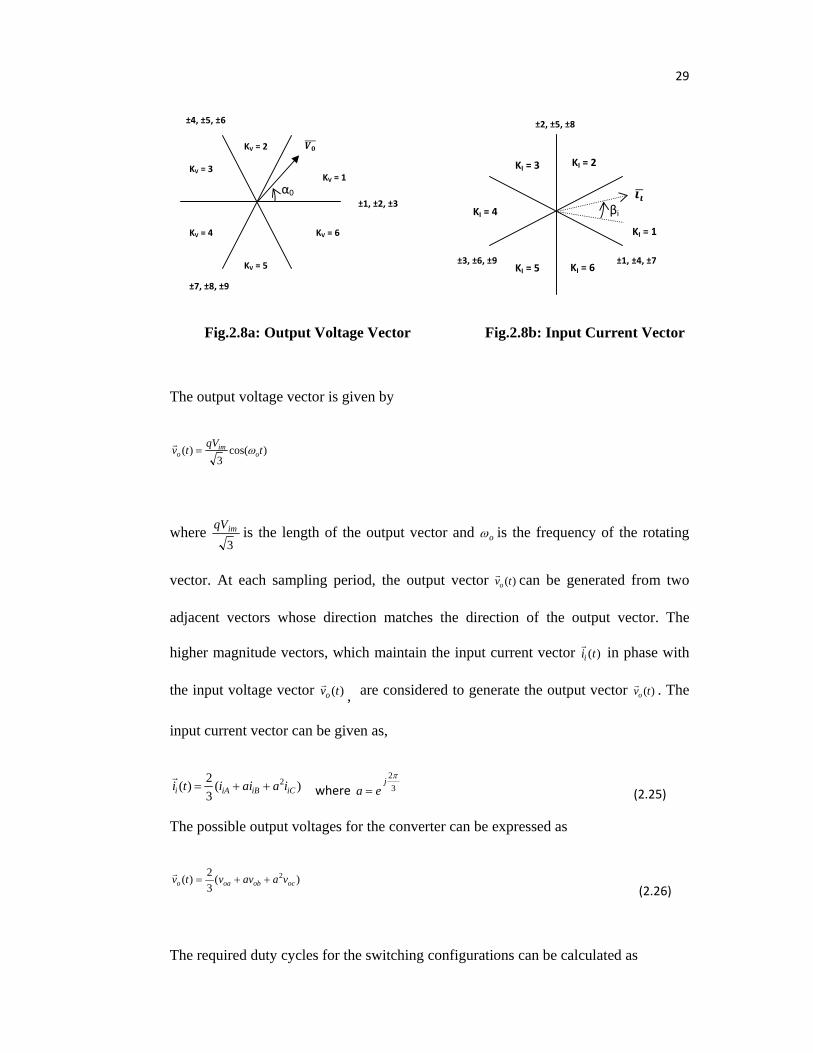
2.4.2 Space Vector Modulation
In Space Vector approach, only one switch in each output phase of MC must be
conducting at a time. Hence, there are 27 possible switching combinations which can
be split into three groups as shown in Table 2.3. Out of the three groups only 21 space
vector groups are useful. Only 18 non-zero space vectors in group-I and 3 zero space
vectors in group-II are used. Fig.2.8a shows the output voltage vector and Fig.2.8b
shows the input current vectors. KV denotes the output voltage vector sector and KI
denotes the input current vector sector. The output phases are indicated as a, b and c
and input phases are indicated as A, B and C.
Table2.3 Selection of switching vector using SVM
29
Fig.2.8a: Output Voltage Vector Fig.2.8b: Input Current Vector
The output voltage vector is given by
where 3imqV is the length of the output vector and oω is the frequency of the rotating
vector. At each sampling period, the output vector )(tvor can be generated from two
adjacent vectors whose direction matches the direction of the output vector. The
higher magnitude vectors, which maintain the input current vector )(tiir
in phase with
the input voltage vector )(tvor
, are considered to generate the output vector )(tvor . The
input current vector can be given as,
where 32πj
ea = (2.25)
The possible output voltages for the converter can be expressed as
)(32)( 2
ocoboao vaavvtv ++=r
(2.26)
The required duty cycles for the switching configurations can be calculated as
KV = 1
KV = 2
KV = 3
KV = 4
KV = 5
KV = 6
±1, ±2, ±3
±4, ±5, ±6
±7, ±8, ±9
α0
±1, ±4, ±7±3, ±6, ±9
βi
±2, ±5, ±8
KI = 1
KI = 2 KI = 3
KI = 4
KI = 5 KI = 6
)cos(3
)( tqVtv oim
o ω=r
)(32)( 2
iCiBiAi iaaiiti ++=r

30
(2.27)
i
i
II qφ
πβπασ
cos
)3
cos()3
cos(
32 0 −+
=
rr
(2.28)
i
i
III qφ
πβπασ
cos
)3
cos()3
cos(
32 0 +−
=
rr
(2.29)
i
i
IV qφ
πβπασ
cos
)3
cos()3
cos(
32 0 −−
=
rr
(2.30)
where oαr , iβ
r
and iφ are the angles of output voltage vector, input current vector and
input phase displacement respectively.
The total modulation duty cycle for the complete modulation period is given as
)(1 10 IVIIIII σσσσσ +++−= (2.31)
For unity and 0.866 input power factor operation,
1≤+++ IVIIIIII σσσσ (2.32)
2.5 Simulation Model
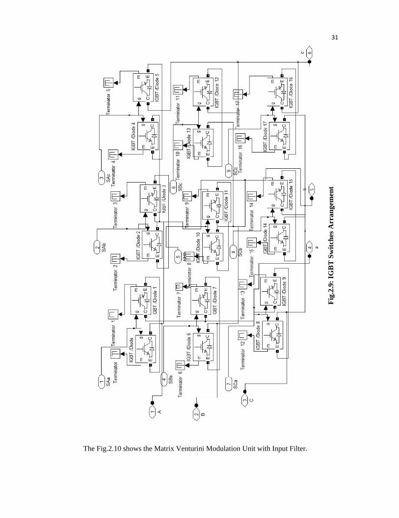
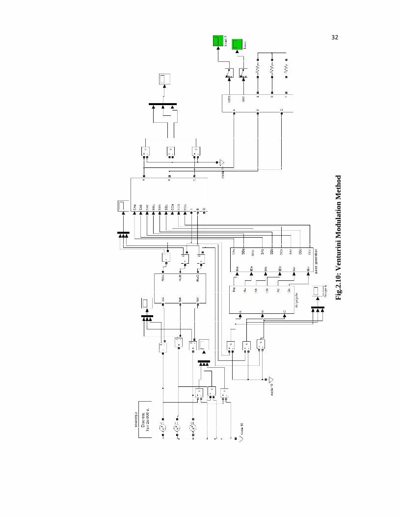
Implementation of MC is done using Matlab / Simulink tools. The Venturini
Algorithm with third harmonic injection and SVM techniques are used to provide the
switching pulses for MC. The MC consists of 9 IGBT switches connected between
each input phase and each output phase as shown in Fig.2.9.
i
i
I qφ
πβπασ
cos
)3
cos()3
cos(
32 0 ++
=
rr
31
The Fig.2.10 shows the Matrix Venturini Modulation Unit with Input Filter.
Fig.
2.9:
IGB
T S
witc
hes A
rran
gem
ent
32
Fig.
2.10
: Ven
turi
ni M
odul
atio
n M
etho
d
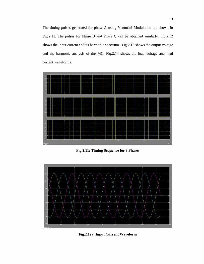
33 The timing pulses generated for phase A using Venturini Modulation are shown in
Fig.2.11. The pulses for Phase B and Phase C can be obtained similarly. Fig.2.12
shows the input current and its harmonic spectrum. Fig.2.13 shows the output voltage
and the harmonic analysis of the MC. Fig.2.14 shows the load voltage and load
current waveforms.
Fig.2.11: Timing Sequence for 3 Phases
Fig.2.12a: Input Current Waveform

34
Fig.2.12b: Harmonic Analysis of Input Current
Fig.2.13a: Input Voltage

35
Fig.2.13b: Harmonic Analysis of Input Voltage
Fig.2.14a: Load Voltage and Load Current

36
Fig.2.14b: Harmonic Analysis of Output Current
The space vector algorithm is also tested with MC. The input voltage, current and
output voltages are analysed for the same load used in Venturini Algorithm method.
Fig.2.15 shows the SVM unit.
Fig.2.15: Space Vector Modulation Unit
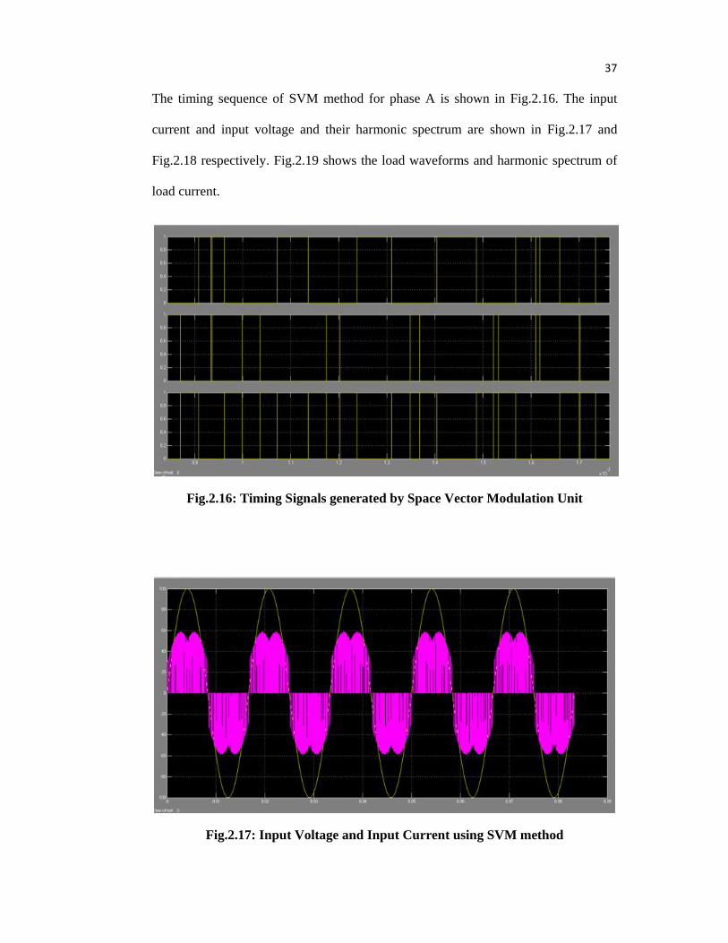
37 The timing sequence of SVM method for phase A is shown in Fig.2.16. The input
current and input voltage and their harmonic spectrum are shown in Fig.2.17 and
Fig.2.18 respectively. Fig.2.19 shows the load waveforms and harmonic spectrum of
load current.
Fig.2.16: Timing Signals generated by Space Vector Modulation Unit
Fig.2.17: Input Voltage and Input Current using SVM method

38
Fig.2.18a: Harmonic Spectrum of Input Voltage
Fig.2.18b: Harmonic Spectrum of Input Current without Filter

39
Fig.2.18c: Harmonic Spectrum of Input Current with Input Filter
Fig.2.19a: Load Voltage and Load Current

40
Fig.2.19b: Harmonic Spectrum of Output Current
It can be seen from the results that the harmonics present in the output and input
currents are less in Venturini Algorithm compared to SVM Algorithm because in
Venturini Algorithm the output voltage and current are calculated independently for
each phase whereas in SVM method the harmonics present in the switching signals
affect the output signals.
2.6 Conclusion
The MC is still not popular in industrial applications because of some practical issues.
The MC is expected to be the “All Silicon Converter”, because it does not need large
reactive elements to store energy. However a study shows that a MC of 4 kW needed
a larger volume of reactive components than a comparable DC link converter [50].
This shows that the MC is not an “All Silicon Converter” and that passive elements in
the form of input filter are needed. More work must be done in order to optimize the
size of the input filter. Another important drawback that is present in MC is the lack
of suitably packaged bi-directional switches. This limitation has recently been

41 overcome with the introduction of power modules which include the complete power
circuit of MC. The most important practical implementation problem in the MC
circuit is the commutation problem between two controlled bi-directional switches.
This has been solved with complicated multistep commutation strategies. The MC is
still facing strong competition from Voltage Source Inverter in terms of cost, size and
reliability. The major problem of MC for use with standard IMs in speed control
applications is the limitation in maximum voltage transfer ratio between the input and
output. In order to overcome this difficulty suitable modulation techniques have to be
derived.
The Venturini, SVM and other methods of modulation based switching techniques
produce output with high level of harmonics. This limits the use of MC in variable
speed operation especially in the application of IM drive circuits. To avoid this
difficulty, more research work has to be focussed on improving the modulation
technique to use MC in IM drive circuits replacing VSCs. The present work is
focussed on implementing the soft computing techniques in modulation strategies to
achieve speed control of IM using MC.