chapter 3 board guide - acrosser, embedded comouter,in · pdf file ·...
TRANSCRIPT

ACM-B6360 Board User Manual
1

Copyright All Rights Reserved. Manual’s first edition:
For the purpose of improving reliability, design and function, the information in this document is subject to change without prior notice and does not represent a commitment on the part of the manufacturer.
In no event will the manufacturer be liable for direct, indirect, special, incidental, or consequential damages arising out of the use or inability to use the product or documentation, even if advised of the possibility of such damages.
This document contains proprietary information protected by copyright. All rights are reserved. No part of this Manual may be reproduced by any mechanical, electronic, or other means in any form without prior written permission of the manufacturer.
Trademarks
ACM-B6360 is a registered trademarks of Acrosser; IBM PC is a registered trademark of the International Business Machines Corporation; Pentium is a registered trademark of Intel Technologies Inc; Award is a registered trademark of Award Software International Inc; other product names mentioned herein are used for identification purposes only and may be trademarks and/or registered trademarks of their respective companies.
2

Table of Contents Chapter 1 Introduction..........................................................................5
1.1 Specifications.......................................................................................................... 5 1.2 Package Contents .................................................................................................... 6 1.3 Block Diagram........................................................................................................ 7
Chapter 2 H/W Information..................................................................8
2.1. Mainboard illustration .......................................................................................... 8 2.2. Locations of IO ports & Jumper settings defination ...................................... 10 2.3. Connectors and Jumper Settings .................................................................... 12 2.4. Specifying the boot BIOS (CN_HDR1 setting).................................................... 17 2.5. Dimension Drawing .............................................................................................. 18
Chapter 3 BIOS Settings.....................................................................19
3.1. Main Setup............................................................................................................ 20 3.2. Advanced Setup .................................................................................................... 22
3.2.1 CPU Configuration ................................................................................. 23 3.2.2 SATA Configuration ................................................................................ 24 3.2.3 Super IO Configuration.......................................................................... 26
3.3. HW Monitor Setup................................................................................................ 27 3.4. Chipset Setup ........................................................................................................ 29
3.4.1 PCH-IO Configuration............................................................................ 30 3.4.2 System Agent (SA) Configuration........................................................ 34
3.5. Boot Setup............................................................................................................. 39 3.5.1 CSM parameters .................................................................................... 41
3.6. Save & Exit Setup................................................................................................. 42
Chapter 4 Driver And Utility Installation ...........................................44
4.1. Driver CD Interface Introduction.......................................................................... 44 4.1.1 Driver Page ............................................................................................... 45 4.1.2 Utility Page ............................................................................................... 51 4.1.3 Application Page....................................................................................... 54 4.1.4 Documents Page........................................................................................ 60
Chapter 5 Software Installation and Programming Guide..................61
3

5.1 API List and Descriptions..................................................................................... 61 5.1.1 GPIO and Watchdog ................................................................................. 61
4
Chapter 1 Introduction ACM-B6360 is a COM Express Type 6 Basic module that fully complies with the PCI Industrial Computer. It supports 3rd Generation Intel ® core TM i7 processors. It integrates Intel ® PCH QM77 chipset. Besides basic I/O ports support like VGA, LVDS, USB2.0, USB3.0, COM. LAN, and GPIO with ACM-B4080 (optional).
1.1 Specifications ACM-B6360 CPU Intel Core i7 3615QE Chipset Intel QM77 chipset Memory SO-DIMM ECC DDR3, Max:16GB RAID support 0, 1, 5, 0+1 OS support Linux Fedora 14, Windows XP, Windows 7, Ubuntu 10 Follow COM Express type 6
ACM-B4080(Optional) Ethernet 1 x RJ45 10/100/1000Mbps LAN ports Serial Port 2 x RS-232 (pin-header, RX/TX signal only) USB 2.0 x 4(pin-header x2, I/O x2), USB3.0 x4(I/O) Flexible GPIO ports (8 bits digital I/O (4 x IN & 4 x OUT) SATA II x2(6.0Gb/s), SATA III x 2(3.0Gb/s) Video VGA (DB15) & LVDS Digital display Interface SDVO x1 & HDMI x2 Audio Line-in, Line-out & MIC phone jack PCIe x16 slot x1, PCIe x4 slot x1, PCIe x1 slot x3 Mini-PCIe x1 (ACM-B6360 not supported) SPI, SMBus, LPC, Port 80 display ATX Form factor
5

1.2 Package Contents Check if the following items are included in the package. Quick Manual ACM-B6360 board 1 x Software Utility CD Screw for Carry Board x5pcs
6

1.3 Block Diagram
7
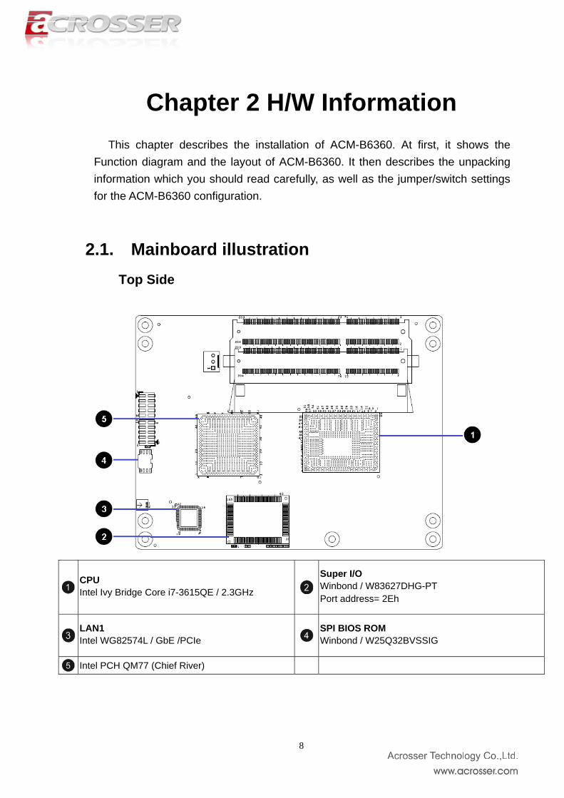
Chapter 2 H/W Information This chapter describes the installation of ACM-B6360. At first, it shows the
Function diagram and the layout of ACM-B6360. It then describes the unpacking information which you should read carefully, as well as the jumper/switch settings for the ACM-B6360 configuration.
2.1. Mainboard illustration Top Side
CPU Intel Ivy Bridge Core i7-3615QE / 2.3GHz
Super I/O Winbond / W83627DHG-PT Port address= 2Eh
LAN1 Intel WG82574L / GbE /PCIe
SPI BIOS ROM Winbond / W25Q32BVSSIG
Intel PCH QM77 (Chief River)
8
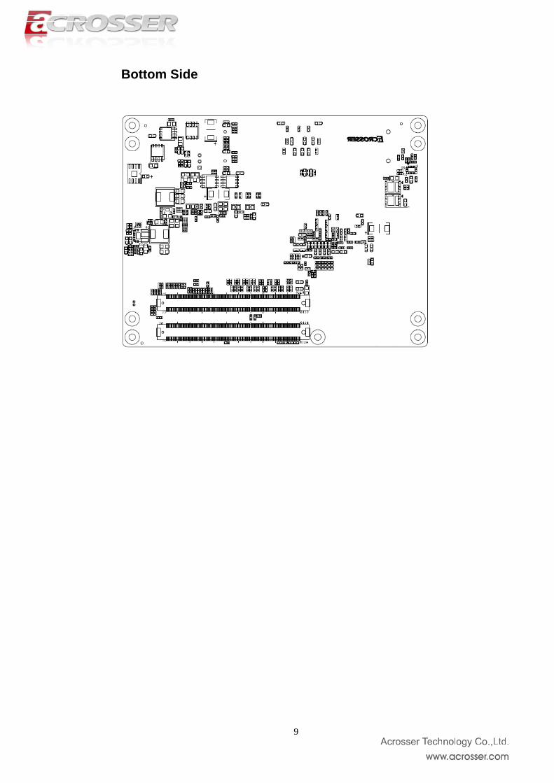
Bottom Side
9
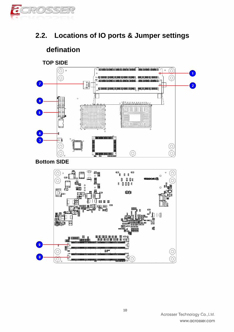
2.2. Locations of IO ports & Jumper settings
defination
TOP SIDE
Bottom SIDE
10

CN_DIMM_2
DDR3 ECC SO-DIMM 204P CN_DIMM_1
DDR3 ECC SO-DIMM 204P
CN_BAT1
WAF-H_1X2P_1.25mm for RTC
Battery connector
CCMOS1
CMOS Memory Clearing PAD SPI1
For BIOS Firmware Update
CN_HDR1 For SPI_CS0# and SPI_CS1# Selection.
CPUFAN1
3 pin FAN connector
CN2
COM Express2.0 Module Type 6 Connector Rows A/B
CN1
COM Express2.0 Module Type 6
Connector Rows C/D
11
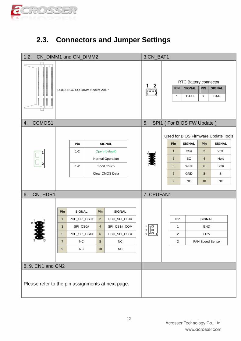
2.3. Connectors and Jumper Settings
1,2. CN_DIMM1 and CN_DIMM2 3.CN_BAT1
DDR3-ECC SO-DIMM Socket 204P
RTC Battery connector PIN SIGNAL PIN SIGNAL
1 BAT+ 2 BAT-
4. CCMOS1 5. SPI1 ( For BIOS FW Update )
Pin SIGNAL
1-2 Open (default)
Normal Operation
1-2 Short Touch
Clear CMOS Data
Used for BIOS Firmware Update Tools
Pin SIGNAL Pin SIGNAL
1 CS# 2 VCC
3 SO 4 Hold
5 WP# 6 SCK
7 GND 8 SI
9 NC 10 NC
6. CN_HDR1 7. CPUFAN1
Pin SIGNAL Pin SIGNAL
1 PCH_SPI_CS0# 2 PCH_SPI_CS1#
3 SPI_CS0# 4 SPI_CS1#_COM
5 PCH_SPI_CS1# 6 PCH_SPI_CS0#
7 NC 8 NC 9 NC 10 NC
Pin SIGNAL
1 GND
2 +12V
3 FAN Speed Sense
8, 9. CN1 and CN2
Please refer to the pin assignments at next page.
12
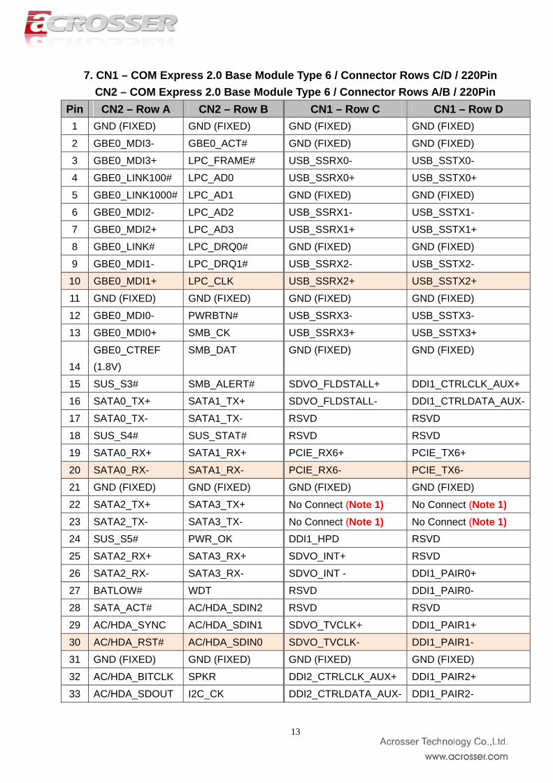
7. CN1 – COM Express 2.0 Base Module Type 6 / Connector Rows C/D / 220Pin CN2 – COM Express 2.0 Base Module Type 6 / Connector Rows A/B / 220Pin
Pin CN2 – Row A CN2 – Row B CN1 – Row C CN1 – Row D 1 GND (FIXED) GND (FIXED) GND (FIXED) GND (FIXED)
2 GBE0_MDI3- GBE0_ACT# GND (FIXED) GND (FIXED)
3 GBE0_MDI3+ LPC_FRAME# USB_SSRX0- USB_SSTX0-
4 GBE0_LINK100# LPC_AD0 USB_SSRX0+ USB_SSTX0+
5 GBE0_LINK1000# LPC_AD1 GND (FIXED) GND (FIXED)
6 GBE0_MDI2- LPC_AD2 USB_SSRX1- USB_SSTX1-
7 GBE0_MDI2+ LPC_AD3 USB_SSRX1+ USB_SSTX1+
8 GBE0_LINK# LPC_DRQ0# GND (FIXED) GND (FIXED)
9 GBE0_MDI1- LPC_DRQ1# USB_SSRX2- USB_SSTX2-
10 GBE0_MDI1+ LPC_CLK USB_SSRX2+ USB_SSTX2+
11 GND (FIXED) GND (FIXED) GND (FIXED) GND (FIXED)
12 GBE0_MDI0- PWRBTN# USB_SSRX3- USB_SSTX3-
13 GBE0_MDI0+ SMB_CK USB_SSRX3+ USB_SSTX3+
14 GBE0_CTREF (1.8V)
SMB_DAT GND (FIXED) GND (FIXED)
15 SUS_S3# SMB_ALERT# SDVO_FLDSTALL+ DDI1_CTRLCLK_AUX+
16 SATA0_TX+ SATA1_TX+ SDVO_FLDSTALL- DDI1_CTRLDATA_AUX-
17 SATA0_TX- SATA1_TX- RSVD RSVD
18 SUS_S4# SUS_STAT# RSVD RSVD
19 SATA0_RX+ SATA1_RX+ PCIE_RX6+ PCIE_TX6+
20 SATA0_RX- SATA1_RX- PCIE_RX6- PCIE_TX6-
21 GND (FIXED) GND (FIXED) GND (FIXED) GND (FIXED)
22 SATA2_TX+ SATA3_TX+ No Connect (Note 1) No Connect (Note 1) 23 SATA2_TX- SATA3_TX- No Connect (Note 1) No Connect (Note 1) 24 SUS_S5# PWR_OK DDI1_HPD RSVD
25 SATA2_RX+ SATA3_RX+ SDVO_INT+ RSVD
26 SATA2_RX- SATA3_RX- SDVO_INT - DDI1_PAIR0+
27 BATLOW# WDT RSVD DDI1_PAIR0-
28 SATA_ACT# AC/HDA_SDIN2 RSVD RSVD
29 AC/HDA_SYNC AC/HDA_SDIN1 SDVO_TVCLK+ DDI1_PAIR1+
30 AC/HDA_RST# AC/HDA_SDIN0 SDVO_TVCLK- DDI1_PAIR1-
31 GND (FIXED) GND (FIXED) GND (FIXED) GND (FIXED)
32 AC/HDA_BITCLK SPKR DDI2_CTRLCLK_AUX+ DDI1_PAIR2+
33 AC/HDA_SDOUT I2C_CK DDI2_CTRLDATA_AUX- DDI1_PAIR2-
13
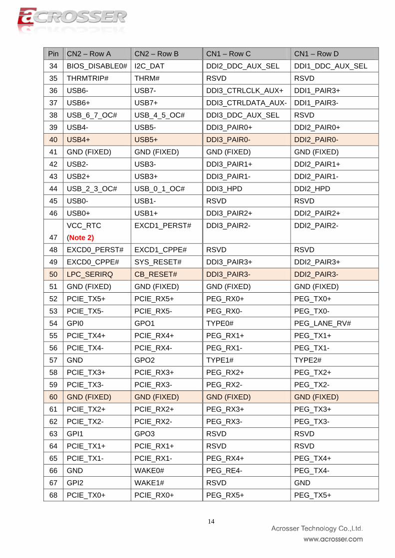
Pin CN2 – Row A CN2 – Row B CN1 – Row C CN1 – Row D
34 BIOS_DISABLE0# I2C_DAT DDI2_DDC_AUX_SEL DDI1_DDC_AUX_SEL
35 THRMTRIP# THRM# RSVD RSVD
36 USB6- USB7- DDI3_CTRLCLK_AUX+ DDI1_PAIR3+
37 USB6+ USB7+ DDI3_CTRLDATA_AUX- DDI1_PAIR3-
38 USB_6_7_OC# USB_4_5_OC# DDI3_DDC_AUX_SEL RSVD
39 USB4- USB5- DDI3_PAIR0+ DDI2_PAIR0+
40 USB4+ USB5+ DDI3_PAIR0- DDI2_PAIR0-
41 GND (FIXED) GND (FIXED) GND (FIXED) GND (FIXED)
42 USB2- USB3- DDI3_PAIR1+ DDI2_PAIR1+
43 USB2+ USB3+ DDI3_PAIR1- DDI2_PAIR1-
44 USB_2_3_OC# USB_0_1_OC# DDI3_HPD DDI2_HPD
45 USB0- USB1- RSVD RSVD
46 USB0+ USB1+ DDI3_PAIR2+ DDI2_PAIR2+
47 VCC_RTC (Note 2)
EXCD1_PERST# DDI3_PAIR2- DDI2_PAIR2-
48 EXCD0_PERST# EXCD1_CPPE# RSVD RSVD
49 EXCD0_CPPE# SYS_RESET# DDI3_PAIR3+ DDI2_PAIR3+
50 LPC_SERIRQ CB_RESET# DDI3_PAIR3- DDI2_PAIR3-
51 GND (FIXED) GND (FIXED) GND (FIXED) GND (FIXED)
52 PCIE_TX5+ PCIE_RX5+ PEG_RX0+ PEG_TX0+
53 PCIE_TX5- PCIE_RX5- PEG_RX0- PEG_TX0-
54 GPI0 GPO1 TYPE0# PEG_LANE_RV#
55 PCIE_TX4+ PCIE_RX4+ PEG_RX1+ PEG_TX1+
56 PCIE_TX4- PCIE_RX4- PEG_RX1- PEG_TX1-
57 GND GPO2 TYPE1# TYPE2#
58 PCIE_TX3+ PCIE_RX3+ PEG_RX2+ PEG_TX2+
59 PCIE_TX3- PCIE_RX3- PEG_RX2- PEG_TX2-
60 GND (FIXED) GND (FIXED) GND (FIXED) GND (FIXED)
61 PCIE_TX2+ PCIE_RX2+ PEG_RX3+ PEG_TX3+
62 PCIE_TX2- PCIE_RX2- PEG_RX3- PEG_TX3-
63 GPI1 GPO3 RSVD RSVD
64 PCIE_TX1+ PCIE_RX1+ RSVD RSVD
65 PCIE_TX1- PCIE_RX1- PEG_RX4+ PEG_TX4+
66 GND WAKE0# PEG_RE4- PEG_TX4-
67 GPI2 WAKE1# RSVD GND
68 PCIE_TX0+ PCIE_RX0+ PEG_RX5+ PEG_TX5+
14
Pin CN2 – Row A CN2 – Row B CN1 – Row C CN1 – Row D 69 PCIE_TX0- PCIE_RX0- PEG_RX5- PEG_TX5-
70 GND(FIXED) GND(FIXED) GND(FIXED) GND(FIXED)
71 LVDS_A0+ LVDS_B0+ PEG_RX6+ PEG_TX6+
72 LVDS_A0- LVDS_B0- PEG_RX6- PEG_TX6-
73 LVDS_A1+ LVDS_B1+ GND(FIXED) GND(FIXED)
74 LVDS_A1- LVDS_B1- PEG_RX7+ PEG_TX7+
75 LVDS_A2+ LVDS_B2+ PEG_RX7- PEG_TX7-
76 LVDS_A2- LVDS_B2- GND GND
77 LVDS_VDD_EN LVDS_B3+ RSVD RSVD
78 LVDS_A3+ LVDS_B3- PEG_RX8+ PEG_TX8+
79 LVDS_A3- LVDS_BKLT_EN PEG_RX8- PEG_TX8-
80 GND(FIXED) GND(FIXED) GND(FIXED) GND(FIXED)
81 LVDS_A_CK+ LVDS_B_CK+ PEG_RX9+ PEG_TX9+
82 LVDS_A_CK- LVDS_B_CK- PEG_RX9- PEG_TX9-
83 LVDS_I2C_CK LVDS_BKLT_CTRL RSVD RSVD
84 LVDS_I2C_DAT VCC_5V_SBY GND GND
85 GPI3 VCC_5V_SBY PEG_RX10+ PEG_TX10+
86 KB_RST# VCC_5V_SBY PEG_RX10- PEG_TX10-
87 A20GATE VCC_5V_SBY GND GND
88 PCIE0_CK_REF+ BIOS_DISABLE1# PEG_RX11+ PEG_TX11+
89 PCIE0_CK_REF- VGA_RED PEG_RX11- PEG_TX11-
90 GND (FIXED) GND (FIXED) GND (FIXED) GND (FIXED)
91 SPI_POWER (3.3V)
VGA_GRN PEG_RX12+ PEG_TX12+
92 SPI_MISO VGA_BLU PEG_RX12- PEG_TX12-
93 GPO0 VGA_HSYNC GND GND
94 SPI_CLK VGA_VSYNC PEG_RX13+ PEG_TX13+
95 SPI_MOSI VGA_I2C_CK PEG_RX13- PEG_TX13-
96 TPM_PP VGA_I2C_DAT GND GND
97 TYPE10# SPI_CS# RSVD RSVD
98 SER0_TX RSVD PEG_RX14+ PEG_TX14+
99 SER0_RX RSVD PEG_RX14- PEG_TX14-
100 GND (FIXED) GND (FIXED) GND (FIXED) GND (FIXED)
101 SER1_TX No Connect PEG_RX15+ PEG_TX15+
102 SER1_RX FAN_TACHIN PEG_RX15- PEG_TX15-
103 LID# SLEEP# GND GND
15
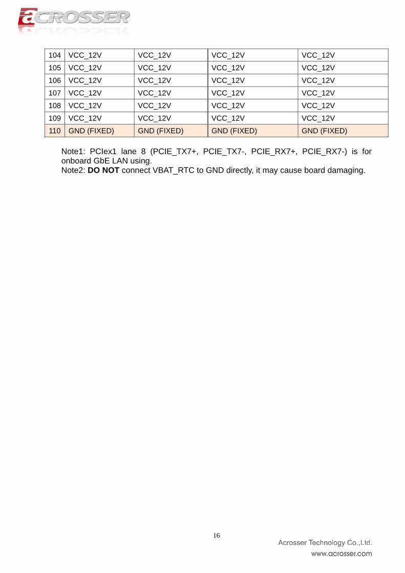
104 VCC_12V VCC_12V VCC_12V VCC_12V
105 VCC_12V VCC_12V VCC_12V VCC_12V
106 VCC_12V VCC_12V VCC_12V VCC_12V
107 VCC_12V VCC_12V VCC_12V VCC_12V
108 VCC_12V VCC_12V VCC_12V VCC_12V
109 VCC_12V VCC_12V VCC_12V VCC_12V
110 GND (FIXED) GND (FIXED) GND (FIXED) GND (FIXED) Note1: PCIex1 lane 8 (PCIE_TX7+, PCIE_TX7-, PCIE_RX7+, PCIE_RX7-) is for onboard GbE LAN using. Note2: DO NOT connect VBAT_RTC to GND directly, it may cause board damaging.
16
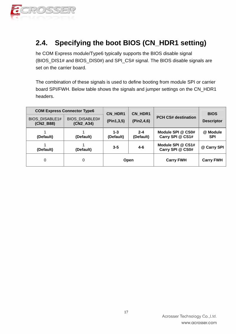
2.4. Specifying the boot BIOS (CN_HDR1 setting) he COM Express module/Type6 typically supports the BIOS disable signal (BIOS_DIS1# and BIOS_DIS0#) and SPI_CS# signal. The BIOS disable signals are set on the carrier board. The combination of these signals is used to define booting from module SPI or carrier board SPI/FWH. Below table shows the signals and jumper settings on the CN_HDR1 headers. COM Express Connector Type6
BIOS_DISABLE1# (CN2_B88)
BIOS_DISABLE0#(CN2_A34)
CN_HDR1
(Pin1,3,5)
CN_HDR1
(Pin2,4,6) PCH CS# destination
BIOS
Descriptor
1 (Default)
1 (Default)
1-3 (Default)
2-4 (Default)
Module SPI @ CS0# Carry SPI @ CS1#
@ Module SPI
1 (Default)
1 (Default) 3-5 4-6 Module SPI @ CS1#
Carry SPI @ CS0# @ Carry SPI
0 0 Open Carry FWH Carry FWH
17
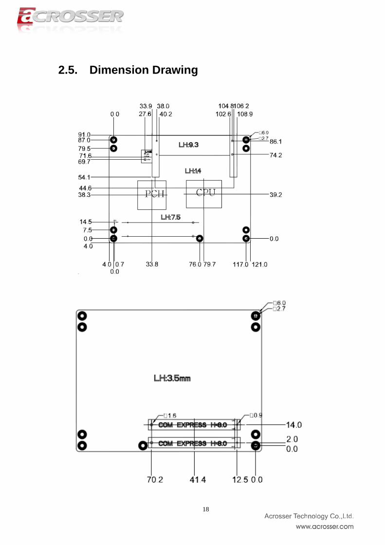
2.5. Dimension Drawing
18
Chapter 3 BIOS Settings
This chapter describes the BIOS menu displays and explains how to perform
common tasks needed to get the system up and running. It also gives detailed explanation of the elements found in each of the BIOS menus. The following topics are covered: Main Setup Advanced Setup HW Monitor Chipset Setup Boot Setup Save Exit Setup
19
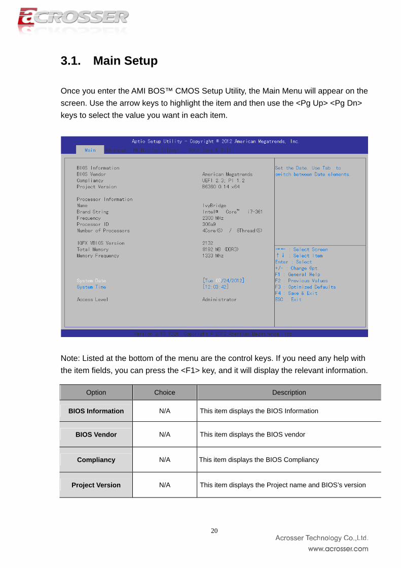
3.1. Main Setup Once you enter the AMI BOS™ CMOS Setup Utility, the Main Menu will appear on the screen. Use the arrow keys to highlight the item and then use the <Pg Up> <Pg Dn> keys to select the value you want in each item.
Note: Listed at the bottom of the menu are the control keys. If you need any help with the item fields, you can press the <F1> key, and it will display the relevant information.
Option Choice Description
BIOS Information N/A This item displays the BIOS Information
BIOS Vendor N/A This item displays the BIOS vendor
Compliancy N/A This item displays the BIOS Compliancy
Project Version N/A This item displays the Project name and BIOS’s version
20
Processor
Information N/A This item displays the CPU Information
Name N/A This item displays the CPU type
Brand String N/A This item displays the CPU processor.
Frequency N/A This item displays the CPU speed.
Processor ID N/A This item displays the CPU processor ID
Number of
Processors N/A This item displays CPU # of cores and Threads.
IGFX VBIOS Version N/A This item displays the VBIOS’s version.
Total Memory N/A This item displays the memory size that used.
Memory Frequency N/A This item displays the memory speed.
System Date N/A Set the system date. Note that the ‘Day’ automatically
changes when you set the date
System Time N/A Set the system time.
Access Level N/A Set the system access level.
21
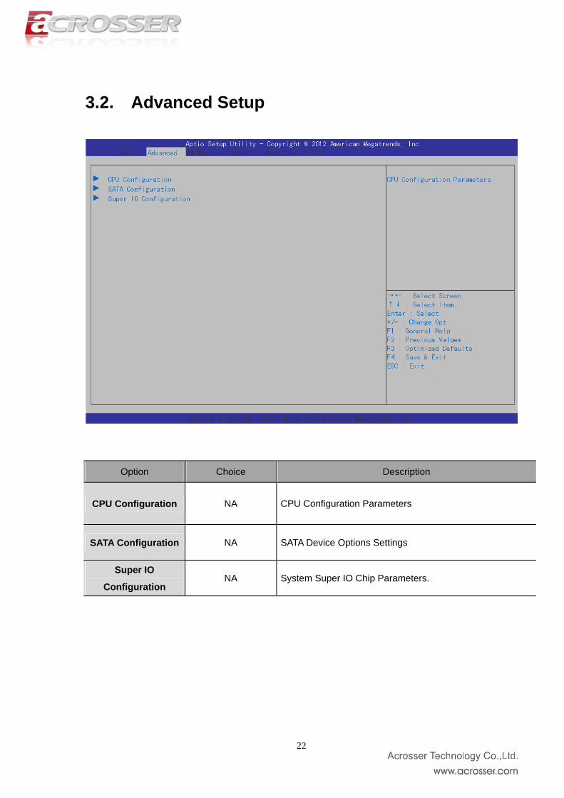
3.2. Advanced Setup
Option Choice Description
CPU Configuration NA CPU Configuration Parameters
SATA Configuration NA SATA Device Options Settings
Super IO
Configuration NA System Super IO Chip Parameters.
22
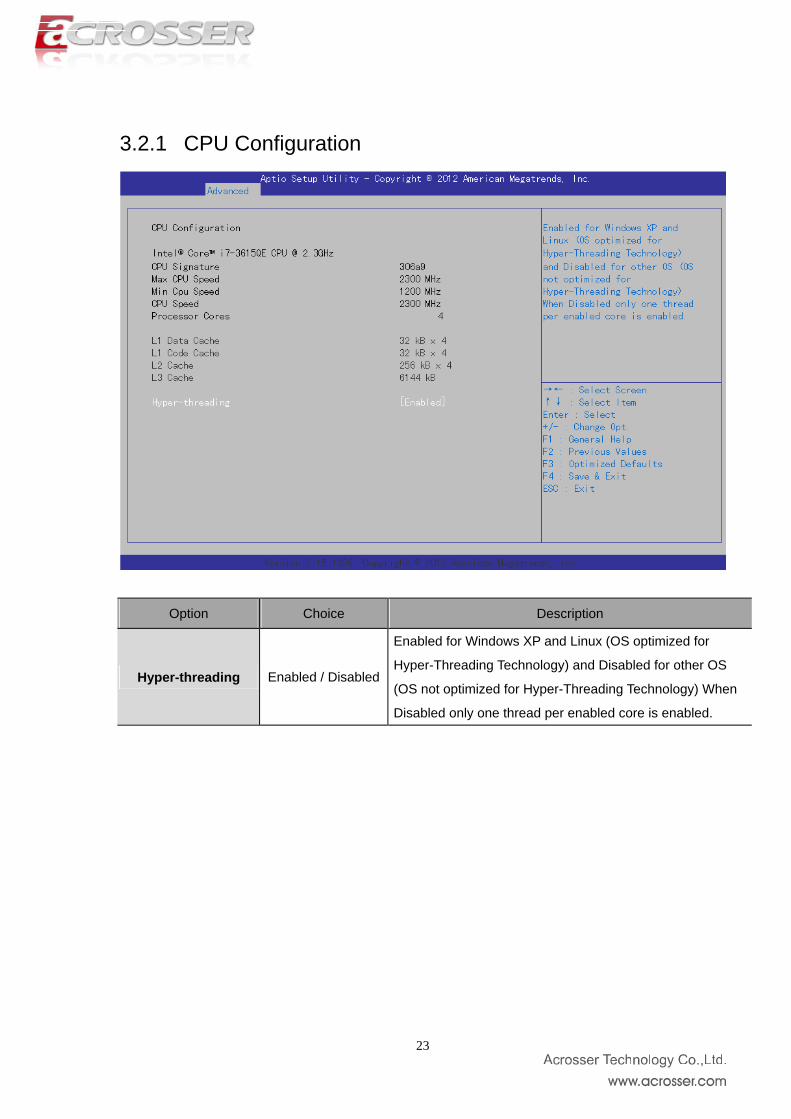
3.2.1 CPU Configuration
Option Choice Description
Hyper-threading Enabled / Disabled
Enabled for Windows XP and Linux (OS optimized for
Hyper-Threading Technology) and Disabled for other OS
(OS not optimized for Hyper-Threading Technology) When
Disabled only one thread per enabled core is enabled.
23
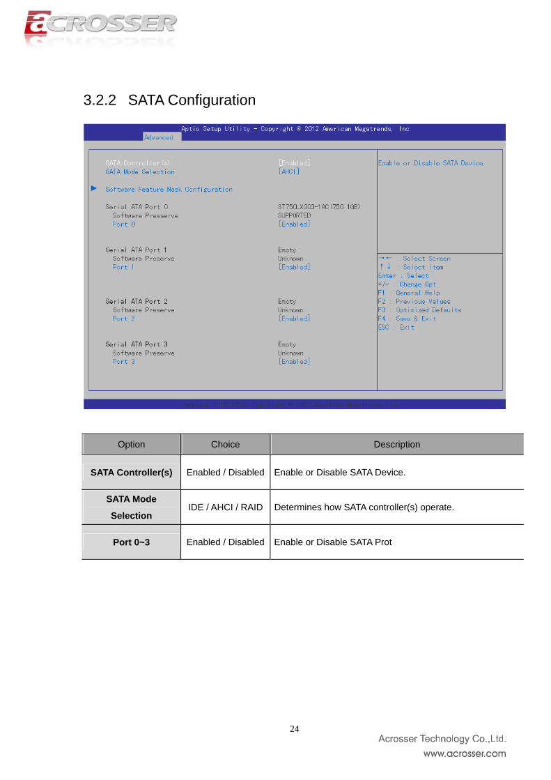
3.2.2 SATA Configuration
Option Choice Description
SATA Controller(s) Enabled / Disabled Enable or Disable SATA Device.
SATA Mode
Selection IDE / AHCI / RAID Determines how SATA controller(s) operate.
Port 0~3 Enabled / Disabled Enable or Disable SATA Prot
24
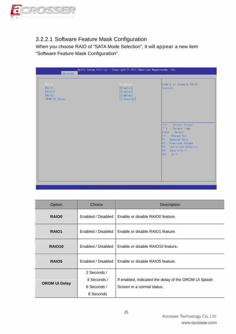
3.2.2.1 Software Feature Mask Configuration When you choose RAID of “SATA Mode Selection”, It will appear a new item “Software Feature Mask Configuration”.
Option Choice Description
RAIO0 Enabled / Disabled Enable or disable RAIO0 feature.
RAIO1 Enabled / Disabled Enable or disable RAIO1 feature.
RAIO10 Enabled / Disabled Enable or disable RAIO10 feature.
RAIO5 Enabled / Disabled Enable or disable RAIO5 feature.
OROM UI Delay
2 Seconds /
4 Seconds /
6 Seconds /
8 Seconds
If enabled, indicated the delay of the OROM UI Splash
Screen in a normal status.
25
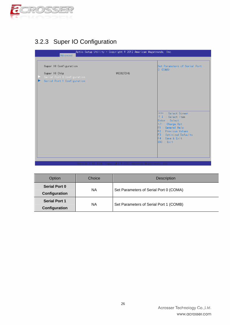
3.2.3 Super IO Configuration
Option Choice Description
Serial Port 0
Configuration NA Set Parameters of Serial Port 0 (COMA)
Serial Port 1
Configuration NA Set Parameters of Serial Port 1 (COMB)
26
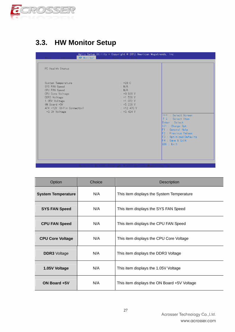
3.3. HW Monitor Setup
Option Choice Description
System Temperature N/A This item displays the System Temperature
SYS FAN Speed N/A This item displays the SYS FAN Speed
CPU FAN Speed N/A This item displays the CPU FAN Speed
CPU Core Voltage N/A This item displays the CPU Core Voltage
DDR3 Voltage N/A This item displays the DDR3 Voltage
1.05V Voltage N/A This item displays the 1.05V Voltage
ON Board +5V N/A This item displays the ON Board +5V Voltage
27

ATX +12V (8-Pin
Connector) N/A This item displays the ATX +12V Voltage
+3.3V Voltage N/A This item displays the +3.3V Voltage
28
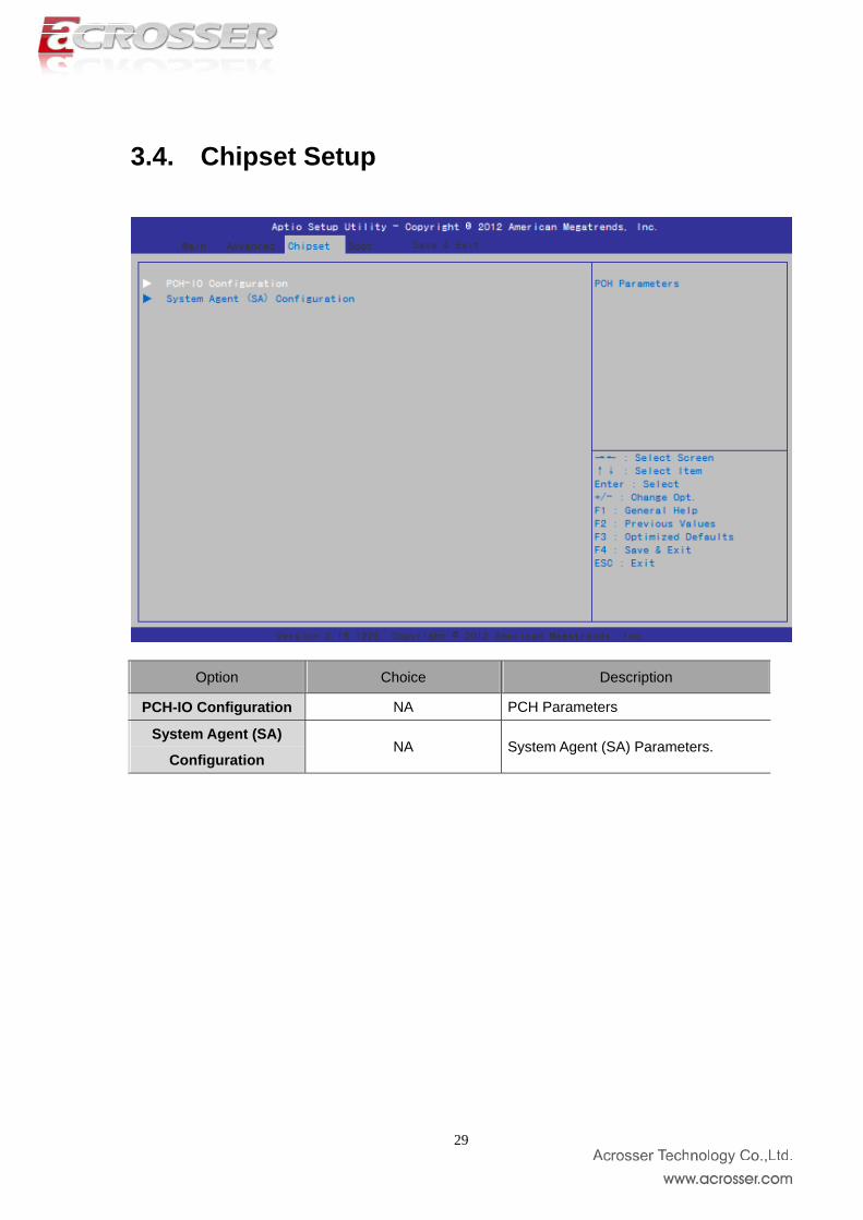
3.4. Chipset Setup
Option Choice Description
PCH-IO Configuration NA PCH Parameters
System Agent (SA)
Configuration NA System Agent (SA) Parameters.
29
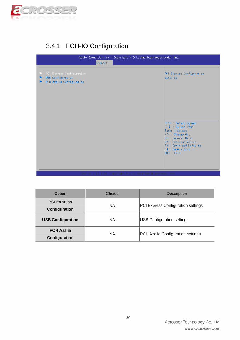
3.4.1 PCH-IO Configuration
Option Choice Description
PCI Express
Configuration NA PCI Express Configuration settings
USB Configuration NA USB Configuration settings
PCH Azalia
Configuration NA PCH Azalia Configuration settings.
30
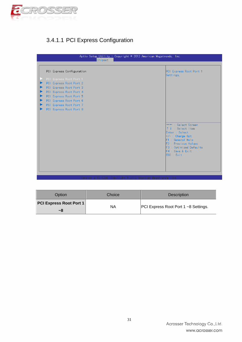
3.4.1.1 PCI Express Configuration
Option Choice Description
PCI Express Root Port 1
~8 NA PCI Express Root Port 1 ~8 Settings.
31
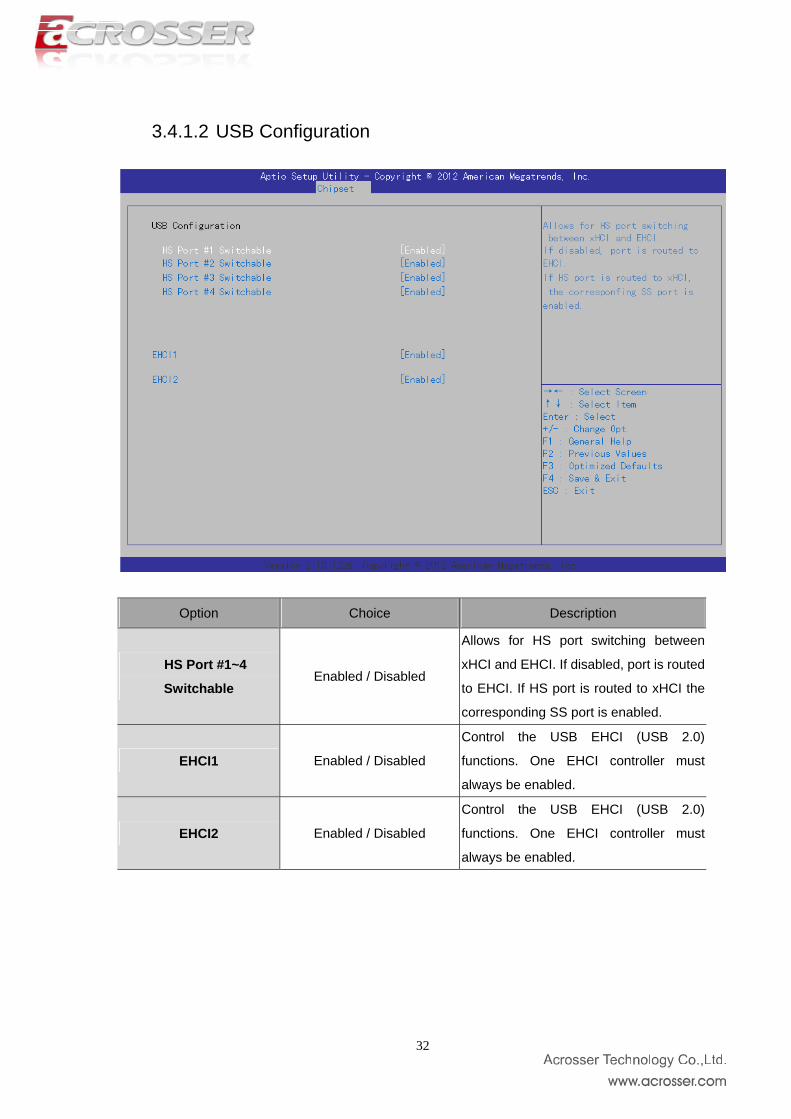
3.4.1.2 USB Configuration
Option Choice Description
HS Port #1~4
Switchable Enabled / Disabled
Allows for HS port switching between
xHCI and EHCI. If disabled, port is routed
to EHCI. If HS port is routed to xHCI the
corresponding SS port is enabled.
EHCI1 Enabled / Disabled
Control the USB EHCI (USB 2.0)
functions. One EHCI controller must
always be enabled.
EHCI2 Enabled / Disabled
Control the USB EHCI (USB 2.0)
functions. One EHCI controller must
always be enabled.
32
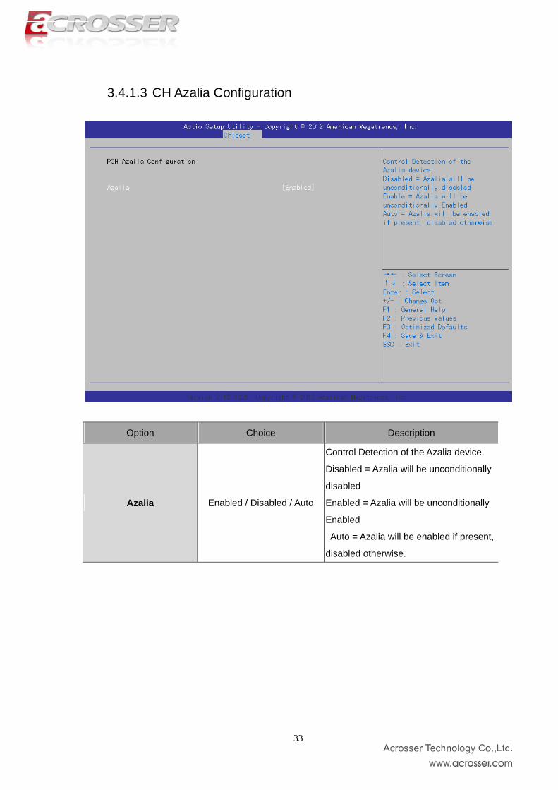
3.4.1.3 CH Azalia Configuration
Option Choice Description
Azalia Enabled / Disabled / Auto
Control Detection of the Azalia device.
Disabled = Azalia will be unconditionally
disabled
Enabled = Azalia will be unconditionally
Enabled
Auto = Azalia will be enabled if present,
disabled otherwise.
33
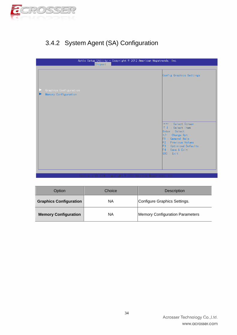
3.4.2 System Agent (SA) Configuration
Option Choice Description
Graphics Configuration NA Configure Graphics Settings.
Memory Configuration NA Memory Configuration Parameters
34
3.4.2.1 Graphics Configuration
Option Choice Description
Primary Display Auto / IGFX / PEG / PCI / SG
Select which of IGFX/PEG/PCI Graphics
device should be Primary Display 0r
select SG for Switchable Gfx.
Internal Graphics Auto / Disabled / Enabled Keep IGD enabled based on the setup
options.
GTT Size 1MB / 2MB Select the GTT Size
Aperture Size 128MB / 256MB / 512MB Select the Aperture Size
DVMT Pre-Allocated
32M / 64M / 96M / 128M /
160M / 192M / 224M / 256M /
288M / 320M / 352M / 384M /
416M / 448M / 480M / 512M /
1024M
Select DVMT 5.0 Pre-Allocated (Fixed)
Graphics Memory size used by the
Internal Graphics Device.
DVMT Total Gfx Mem 128M / 258M / MAX
Select DVMT 5.0 Total Graphics Memory
size used by the Internal Graphics
Device.
35
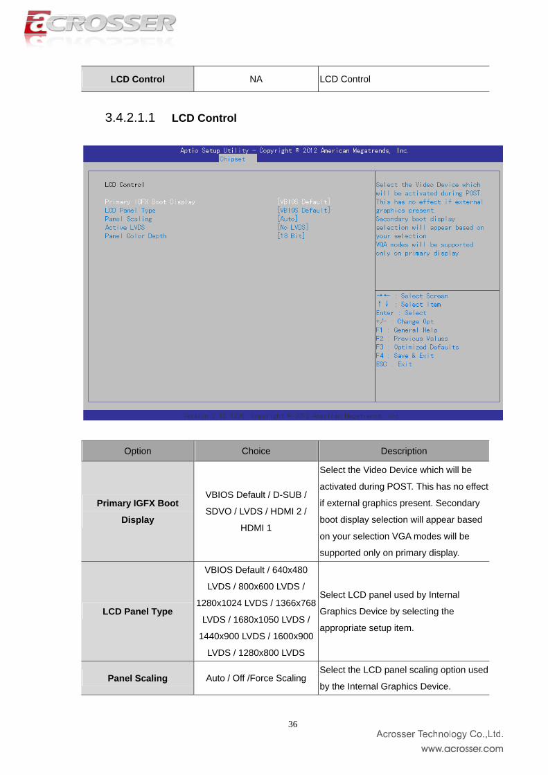
LCD Control NA LCD Control
3.4.2.1.1 LCD Control
Option Choice Description
Primary IGFX Boot
Display
VBIOS Default / D-SUB /
SDVO / LVDS / HDMI 2 /
HDMI 1
Select the Video Device which will be
activated during POST. This has no effect
if external graphics present. Secondary
boot display selection will appear based
on your selection VGA modes will be
supported only on primary display.
LCD Panel Type
VBIOS Default / 640x480
LVDS / 800x600 LVDS /
1280x1024 LVDS / 1366x768
LVDS / 1680x1050 LVDS /
1440x900 LVDS / 1600x900
LVDS / 1280x800 LVDS
Select LCD panel used by Internal
Graphics Device by selecting the
appropriate setup item.
Panel Scaling Auto / Off /Force Scaling Select the LCD panel scaling option used
by the Internal Graphics Device.
36

Active LVDS No LVDS/ Int-LVDS
Select the Active LFP Configuration. No
LVDS: VBIOS does not enable LVDS.
Int-LVDS: VBIOS enables LVDS driver by
Integrated encoder. SDVO LVDS: VBIOS
enables LVDS driver by SDVO encoder.
eDP Port-A: LFP Driven by
Int-DisplayPort encoder from Port-A.
Panel Color Depth 18 Bit /24 Bit Select the LFP Panel Color Depth
37
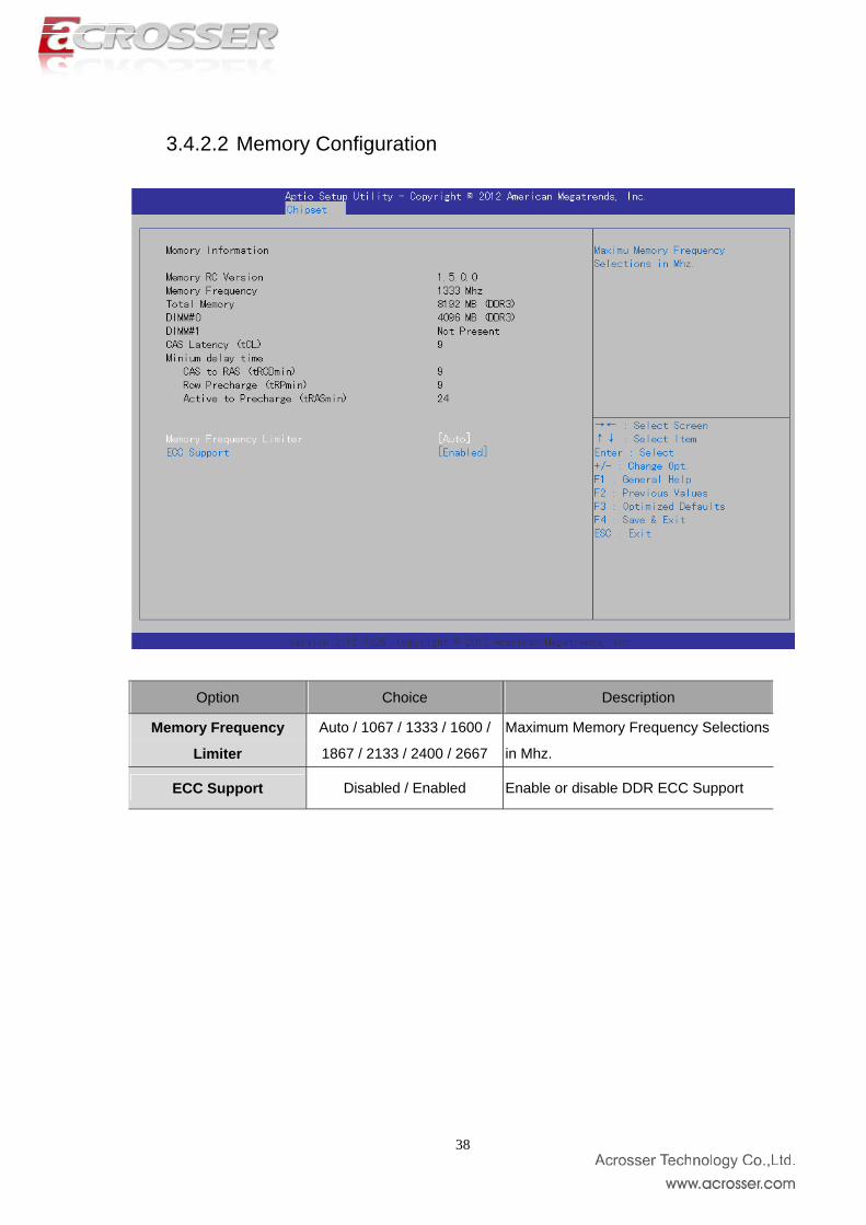
3.4.2.2 Memory Configuration
Option Choice Description
Memory Frequency
Limiter
Auto / 1067 / 1333 / 1600 /
1867 / 2133 / 2400 / 2667
Maximum Memory Frequency Selections
in Mhz.
ECC Support Disabled / Enabled Enable or disable DDR ECC Support
38

3.5. Boot Setup
Option Choice Description
Boot up Num Lock
State On / Off Select the keyboard Num Lock State
Boot Loge Disabled / Enabled Enables or disables Quiet Boot option
Fast Boot Disabled / Enabled
Enables or disables boot with initialization of a minimal set
of devices required to launch active boot option. Has no
effect for BBS boot options.
Boot Option #1
IBA GE Slot 0200
v1322 / UEFI: IP4
Intel ® 82574L
Gigabit Network
Connection / UEFI:
IP6 Intel ® 82574L
Gigabit Network
Sets the system boot order
39
Connection /
Disabled
Boot Option #2
IBA GE Slot 0200
v1322 / UEFI: IP4
Intel ® 82574L
Gigabit Network
Connection / UEFI:
IP6 Intel ® 82574L
Gigabit Network
Connection /
Disabled
Sets the system boot order
Network Device BBS
Priorities NA Set the order of the legacy devices in this group
Hard Drive BBS
Priorities NA Set the order of the legacy devices in this group
CSM parameters NA Op ROM execution, boot options filter, etc.
40
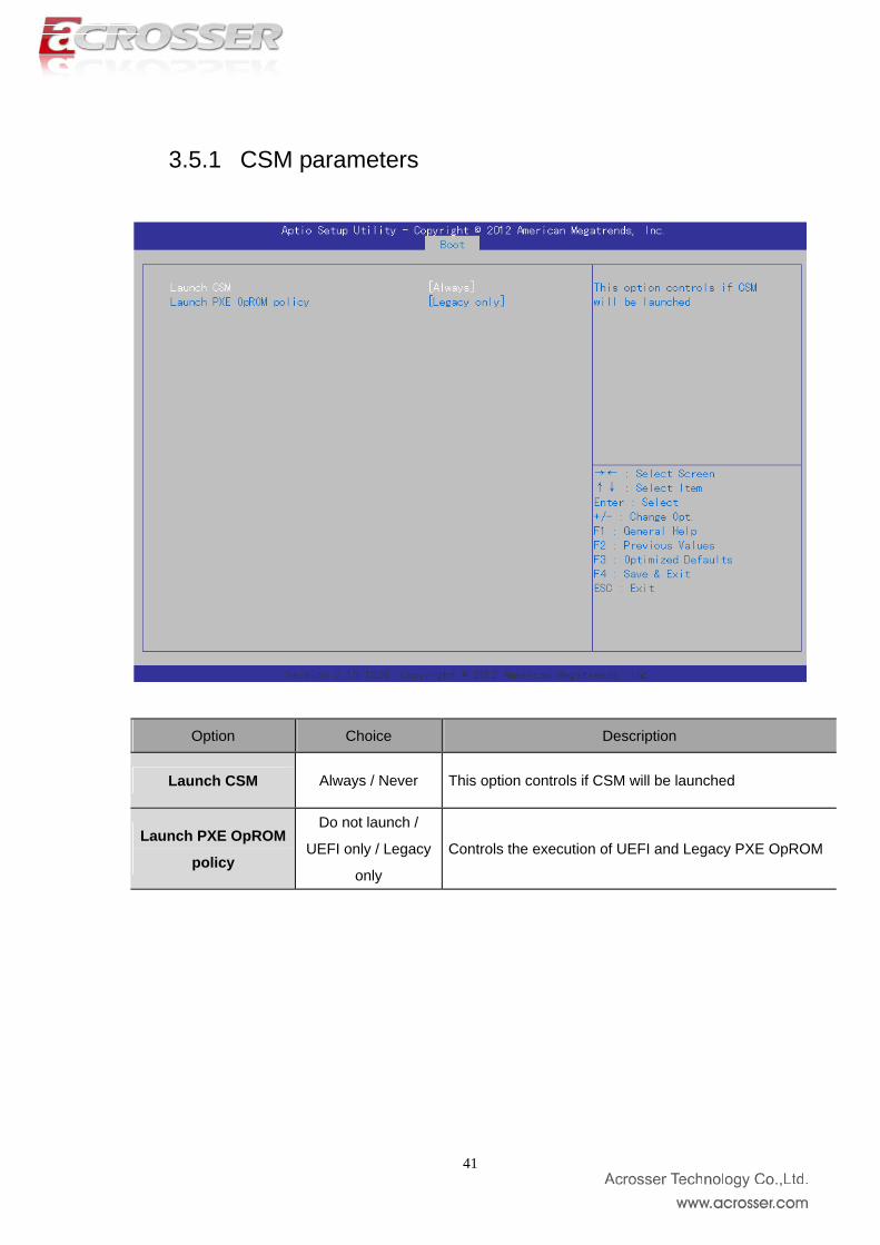
3.5.1 CSM parameters
Option Choice Description
Launch CSM Always / Never This option controls if CSM will be launched
Launch PXE OpROM
policy
Do not launch /
UEFI only / Legacy
only
Controls the execution of UEFI and Legacy PXE OpROM
41
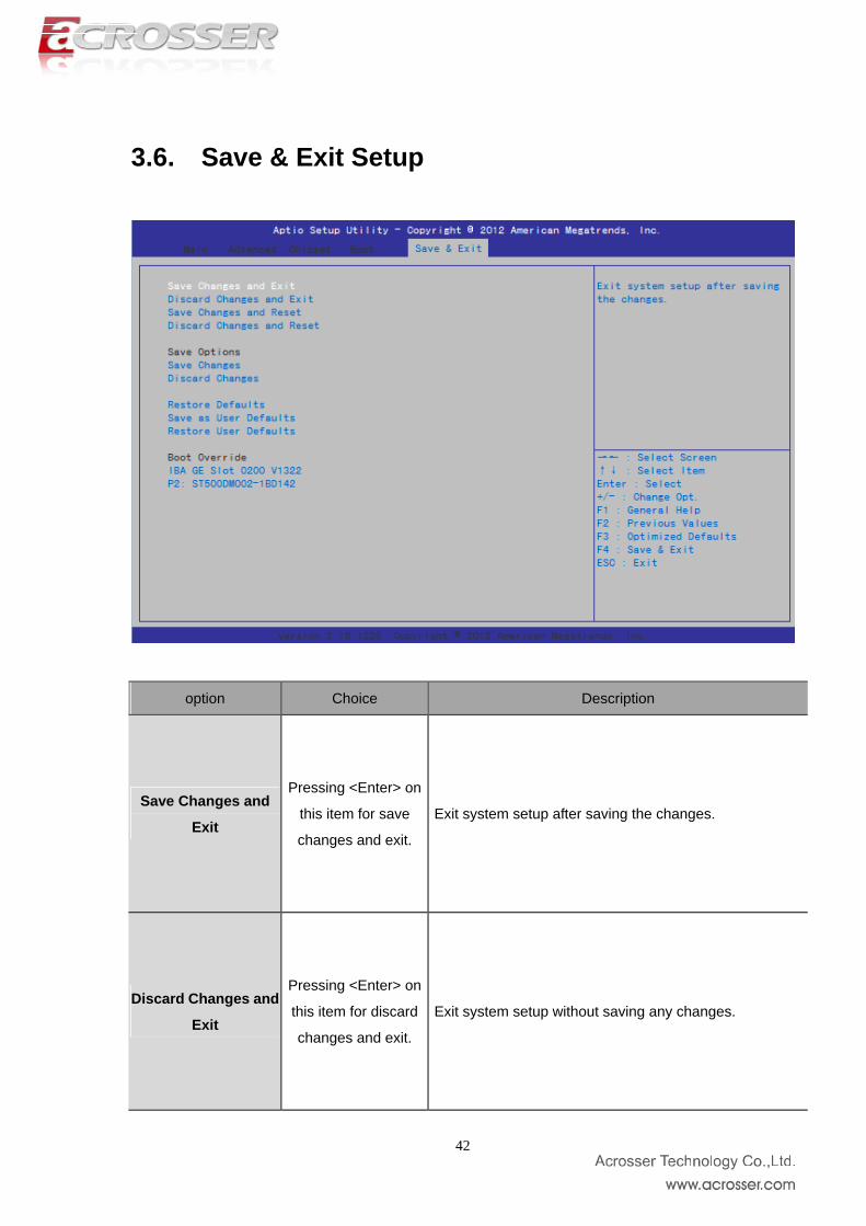
3.6. Save & Exit Setup
option Choice Description
Save Changes and
Exit
Pressing <Enter> on
this item for save
changes and exit.
Exit system setup after saving the changes.
Discard Changes and
Exit
Pressing <Enter> on
this item for discard
changes and exit.
Exit system setup without saving any changes.
42
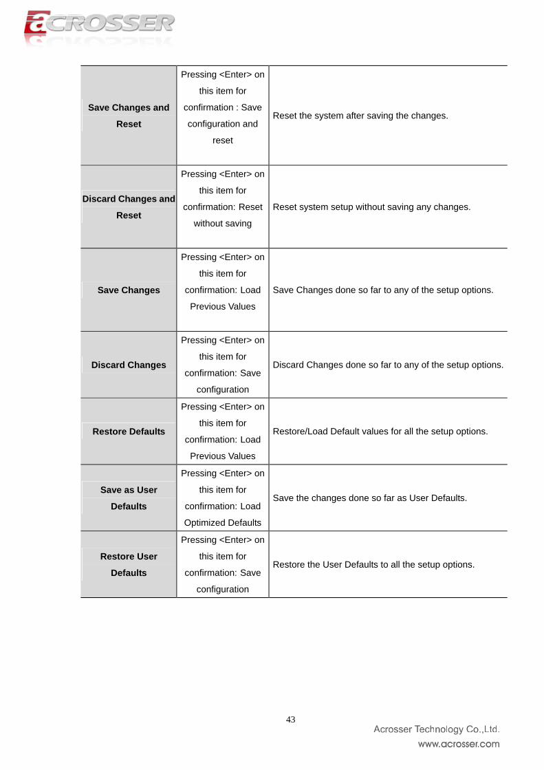
Save Changes and
Reset
Pressing <Enter> on
this item for
confirmation : Save
configuration and
reset
Reset the system after saving the changes.
Discard Changes and
Reset
Pressing <Enter> on
this item for
confirmation: Reset
without saving
Reset system setup without saving any changes.
Save Changes
Pressing <Enter> on
this item for
confirmation: Load
Previous Values
Save Changes done so far to any of the setup options.
Discard Changes
Pressing <Enter> on
this item for
confirmation: Save
configuration
Discard Changes done so far to any of the setup options.
Restore Defaults
Pressing <Enter> on
this item for
confirmation: Load
Previous Values
Restore/Load Default values for all the setup options.
Save as User
Defaults
Pressing <Enter> on
this item for
confirmation: Load
Optimized Defaults
Save the changes done so far as User Defaults.
Restore User
Defaults
Pressing <Enter> on
this item for
confirmation: Save
configuration
Restore the User Defaults to all the setup options.
43
Chapter 4 Driver And Utility Installation
4.1. Driver CD Interface Introduction Acrosser provides the a driver CD, which includes the drivers, utilities,
applications and documents. For Windows environment, it can be guided by the setup program; for Linux environment, the related files can be found at folder “ACMB6360\Linux”.
Once putting the CD into the optical disk drive, it will run automatically. The driver CD will also detect the MB information to see if they are matched. The following error messages appear if you get an incorrect driver CD.
It indicates that the board information is not available.
It indicates that the program gets wrong board information.
44
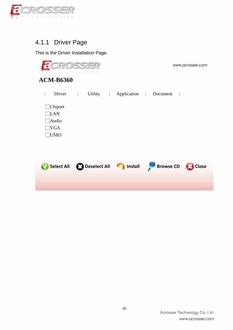
4.1.1 Driver Page This is the Driver Installation Page.
ACM-B6360
︱ Driver ︱ Utility ︱ Application ︱ Document ︱
□Chipset □LAN □Audio □VGA □USB3
45

Click the icon, all the drivers will be selected.
ACM-B6360
︱ Driver ︱ Utility ︱ Application ︱ Document ︱
Chipset LAN Audio VGA USB3
46
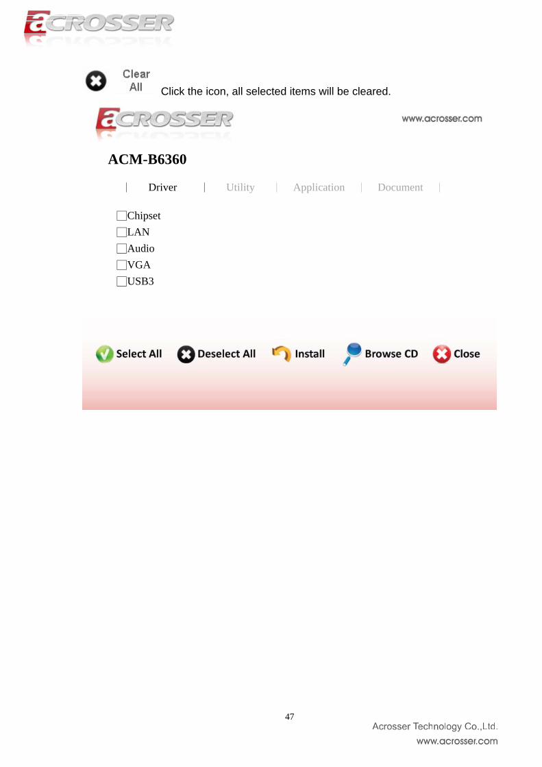
Click the icon, all selected items will be cleared.
︱ Driver ︱ Utility ︱ Application ︱ Document ︱
ACM-B6360
□Chipset □LAN □Audio □VGA □USB3
47

Click the icon to install the selected drivers. The progress bar shows up. The main window will temporarily disappear.
48
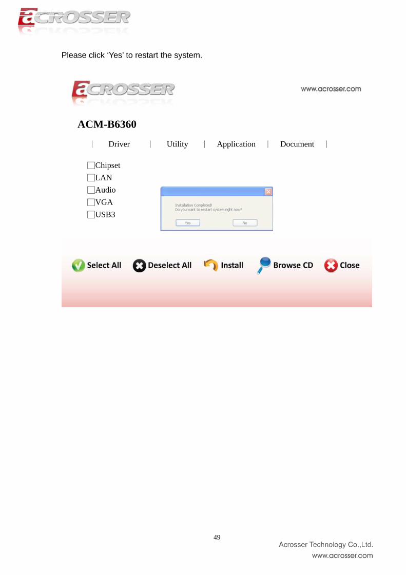
Please click ‘Yes’ to restart the system.
ACM-B6360
︱ Driver ︱ Utility ︱ Application ︱ Document ︱
□Chipset □LAN □Audio □VGA □USB3
49

Click this icon to browse this CD content.
50
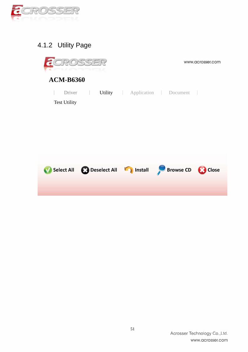
4.1.2 Utility Page
Test Utility
ACM-B6360
︱ Driver ︱ Utility ︱ Application ︱ Document ︱
51
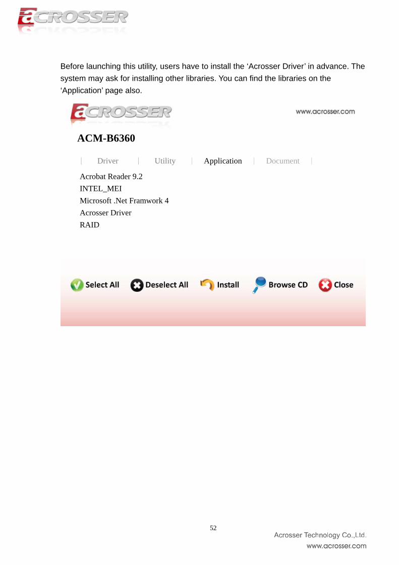
Before launching this utility, users have to install the ‘Acrosser Driver’ in advance. The system may ask for installing other libraries. You can find the libraries on the ‘Application’ page also.
ACM-B6360
Acrobat Reader 9.2 INTEL_MEI Microsoft .Net Framwork 4 Acrosser Driver RAID
︱ Driver ︱ Utility ︱ Application ︱ Document ︱
52

This is the test utility.
53
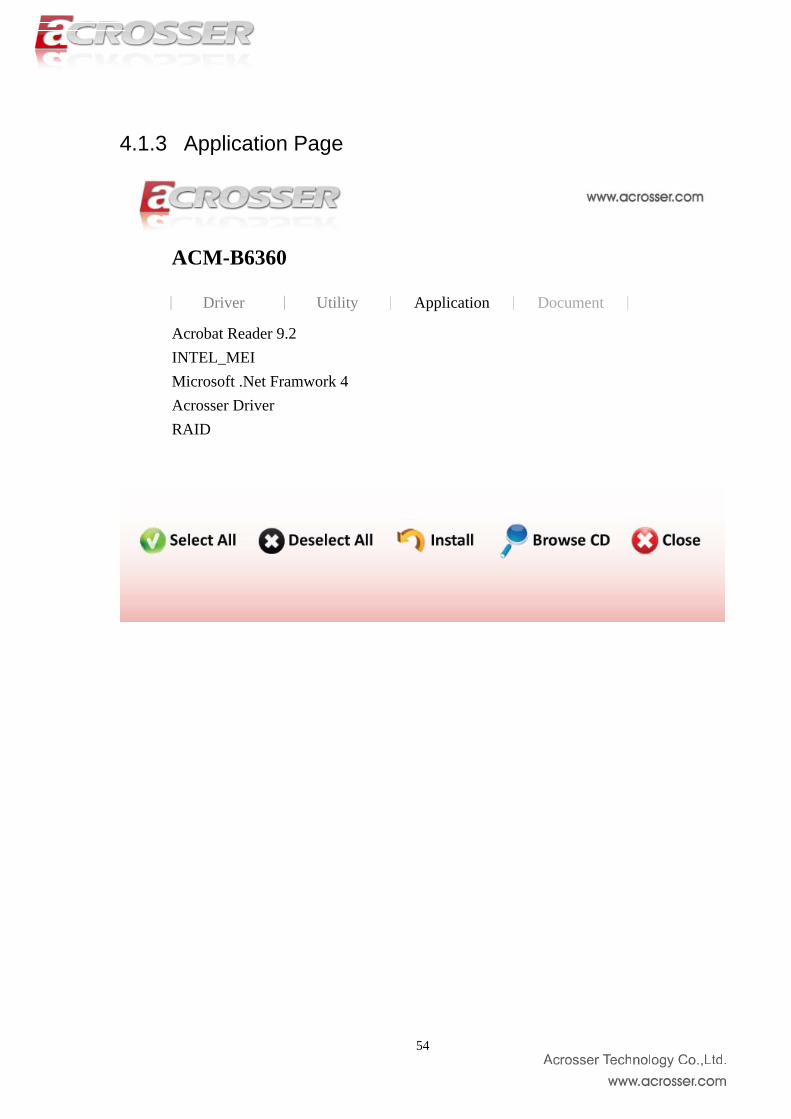
4.1.3 Application Page
ACM-B6360
Acrobat Reader 9.2 INTEL_MEI Microsoft .Net Framwork 4Acrosser Driver RAID
︱ Driver ︱ Utility ︱ Application ︱ Document ︱
54
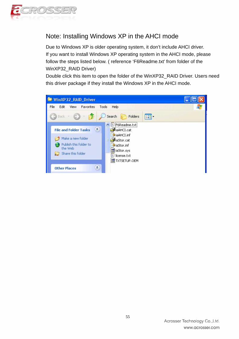
Note: Installing Windows XP in the AHCI mode Due to Windows XP is older operating system, it don’t include AHCI driver. If you want to install Windows XP operating system in the AHCI mode, please follow the steps listed below. ( reference ‘F6Readme.txt’ from folder of the WinXP32_RAID Driver) Double click this item to open the folder of the WinXP32_RAID Driver. Users need this driver package if they install the Windows XP in the AHCI mode.
55
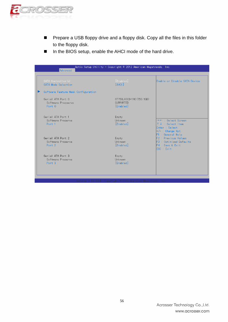
Prepare a USB floppy drive and a floppy disk. Copy all the files in this folder
to the floppy disk. In the BIOS setup, enable the AHCI mode of the hard drive.
56
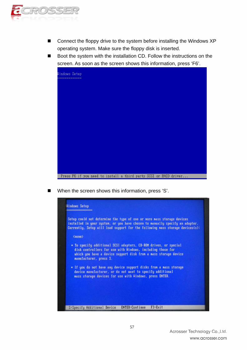
Connect the floppy drive to the system before installing the Windows XP
operating system. Make sure the floppy disk is inserted. Boot the system with the installation CD. Follow the instructions on the
screen. As soon as the screen shows this information, press ‘F6’.
When the screen shows this information, press ‘S’.
57
58
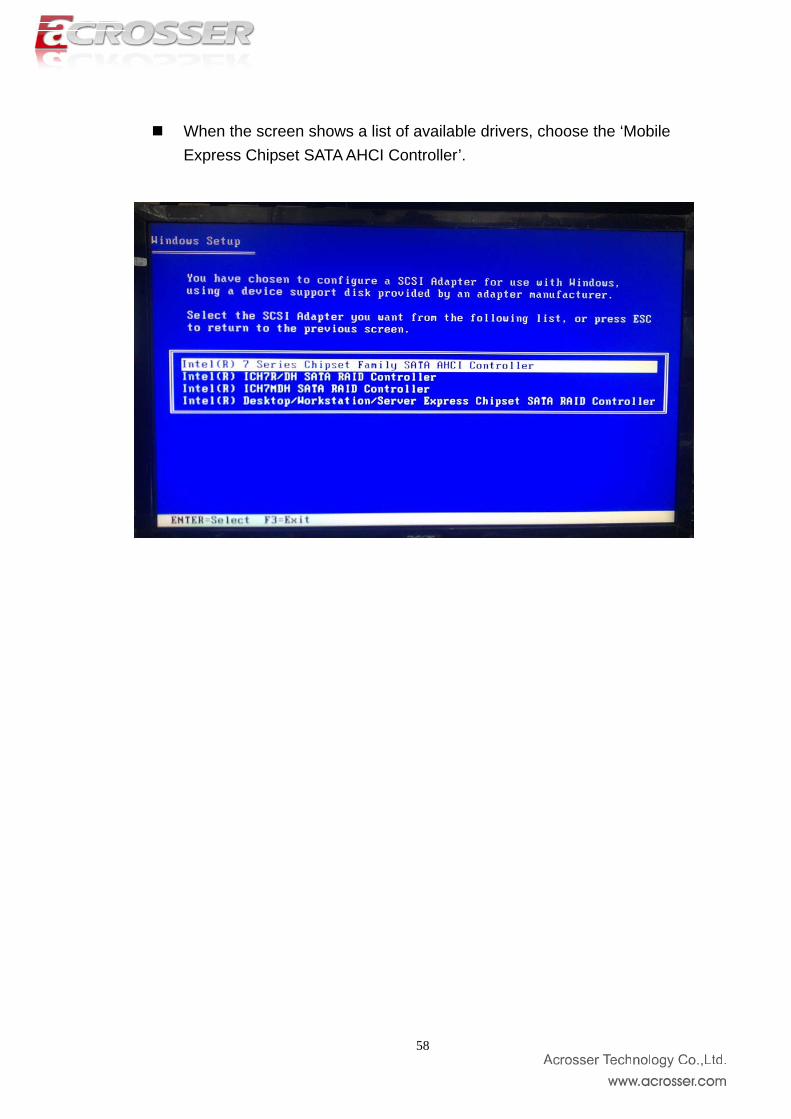
When the screen shows a list of available drivers, choose the ‘Mobile
Express Chipset SATA AHCI Controller’.
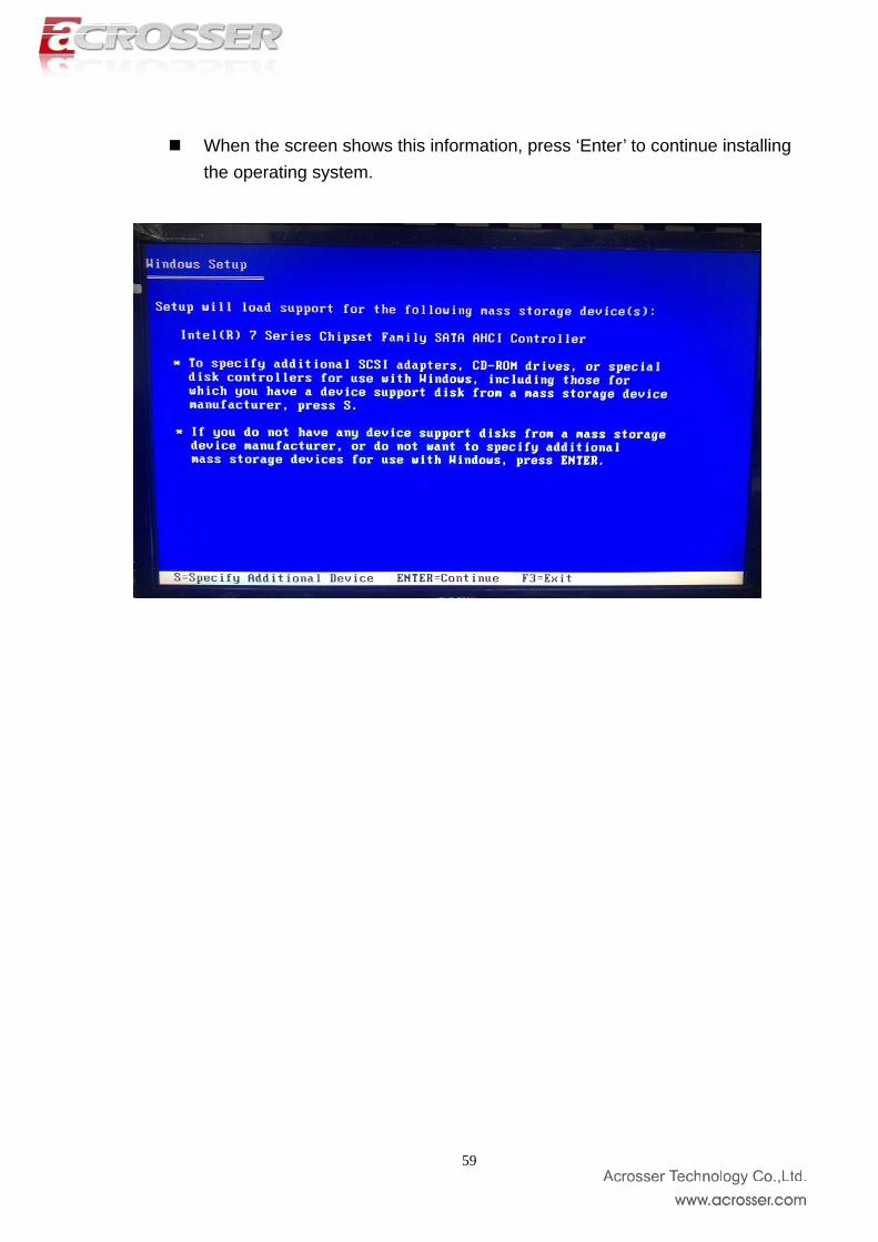
When the screen shows this information, press ‘Enter’ to continue installing
the operating system.
59
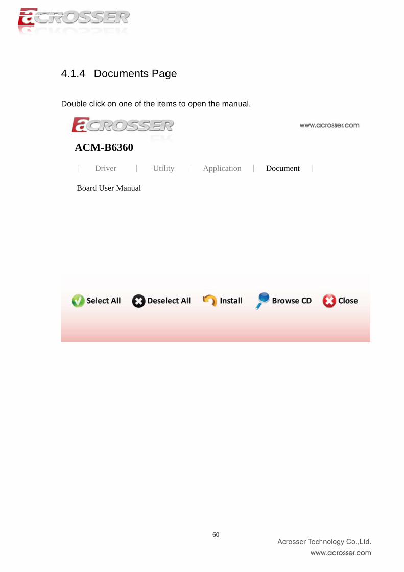
4.1.4 Documents Page Double click on one of the items to open the manual.
ACM-B6360
︱ Driver ︱ Utility ︱ Application ︱ Document ︱
Board User Manual
60
Chapter 5 Software Installation and Programming Guide
5.1 API List and Descriptions
5.1.1 GPIO and Watchdog 5.1.1.1 Overview
This model provides both a GPIO interface and a Watchdog timer. Users can use the GPIO and Watchdog APIs to configure and to access the GPIO interface and the Watchdog timer. The GPIO has four input pins and four output pins. The Watchdog timer can be set to 1~255 seconds. Setting the timer to zero disables the timer. The remaining seconds of the timer to reboot can be read from the timer.
5.1.1.2 GPIO(Linux) 1. Syntax:
Get_gpio_status(int pin)
Description: Get the status of GPIO input pins and output pins status. Parameters: This function takes a pointer to an unsigned char variable as the parameter. The pin0 ~ 3 is the status of the output pins. The pin4 ~ pin7 is the status of the input pins. Return Value: 1:HIGH, 0:LOW.
2. Syntax:
Set_gpio(int pin, int value)
Description: Set the status of GPIO Output value. Parameters:
61
Set value 0 is Low, 1 is High Return Value: If the function sets the values successfully, it returns 0 or -1, any other returned value stands for error.
5.1.1.3 GPIO (Windows) 1. Syntax:
getChLevel(u8 *val)
Description: Get the status of GPIO input pins and output pins, and put the value at *val. Parameters: This function takes a pointer to an unsigned char variable as the parameter. The bit0 ~ bit3 in the pointed variable ‘*val’ is the status of the output pins. The bit4 ~ bit7 in the pointed variable ‘*val’ is the status of the input pins. Return Value: If the function gets the value successfully, it returns 0 or -1, any other returned value stands for error.
2. Syntax:
Set_gpio(int pin, int value)
Description: Set the status of GPIO Output value. Parameters: Set value 0 is Low, 1 is High
5.1.1.4 Watchdog (Liunx) 1. Syntax:
Wdt_start(Void)
Description: This function of the watchdog time to start counter. Parameters: The parameter ‘val’ is the value to set to watchdog timer register. The range is 1~ 255 . Return Value: None.
62

2. Syntax:
Wdt_stop(Void)
Description: Any time call this function will stop Watchdog Timer. Parameters: None. Return Value: None.
3. Syntax: Get_wdt_count()
Description: This function read the value of the watchdog time counter. Parameters: None. Return Value: This function returns the value of the time counter.
5.1.1.5 Watchdog (Windows) 1. Syntax:
setWtdTimer(u8 value)
Description: This function of the watchdog time to start counter. Parameters: The parameter ‘value’ is the value to set to watchdog timer register. The range is 1~ 255 . Return Value: None.
2. Syntax: getWtdTimer(void)
Description: This function read the value of the watchdog time counter. Parameters: None. Return Value: This function returns the value of the time counter.
63