chapter 3 fpga interfacing with...
TRANSCRIPT

20
CHAPTER 3
FPGA INTERFACING WITH MICROCONTROLLER
3.1 Microcontroller based FPGA System Devices
Microcontroller and FPGA have an extensive use in digital system mainly
because of low price and high speed. They are having a great role in embedded system
design and in the area of intelligent sensors and automation [66]-[75].
Dealing with the Microcontrollers is not a great concern. But the problem
arises, when Microcontroller needs to be interfaced with the outside world in an
academic environment, and this is due to the lack of resources and time [69].
Now the question arises that how to interface the Microcontroller in order to
exploit its maximum usage.[67],[68] The answer is FPGA, and we are aware that FPGA
devices with its feature of reconfiguration allows its designers to be more user friendly
and provide flexibility.
Implementing the design with FPGA is highly abstract in nature and hide the
complexity from the user. Moreover, designing digital system with FPGA can be done
easily on a laptop or desktop computers.
FPGA technology and Microcontroller technology are both having dominant
presence in the digital system design industry [73] and we are aware of the importance
of these technologies when they are being used as stand alone, but now we have to see
that how these technologies can be clubbed together for different applications.
21
3.1.1 Microcontrollers and FPGAs
In today’s world, Microcontrollers are playing a greater role in our
technological applications and especially for embedded driven applications such as
modems, car control, appliances etc [66]. All this is possible because of the
extraordinary specifications of the Microcontrollers such as communications, timing,
memory and data conversion functions. But the need of these specifications are different
for different applications such as some applications will require more memory or some
applications will require fast timing or execution. So in order to meet such requirements,
the designer can have an add on circuit to implement these specific functions.
Due to low cost and high speed FPGAs are often a perfect choice for
implementing such functions.[11]-[18] But in order to exploit such devices one must be
having a sufficient knowledge of both Microcontrollers and FPGAs . Moreover, it
strictly depends upon the designer that the application can be developed using only the
stand alone Microcontroller or it requires the support of FPGA [68]. But nothing comes
free hand, we have to be very cautious in choosing the system because the design
variables may get affected and can lead to an improper design.
In our Research work we had interfaced two AVR8515 Microcontrollers[65]
with a dual port memory implemented in Xilinx Spartan 3 FPGA[59]-[61] .The main
aim of this work is to show that if your application requires more memory than the
Microcontrollers have, then you can use the additional memory implemented in FPGA
device.
3.1.2 Microcontrollers and FPGA based Embedded System Applications
Embedded system applications are based on software and hardware
partitioning [67], design variable such as price and performance are the major criteria
for choosing the hardware and software partitioning.
Conventional embedded system basically used specialized general purpose
chips that are having a fixed dedicated logic which could not be altered, where as FPGA
on the other hand offers easy reprogram ability and change of digital logic by
downloading new bit stream representing new circuit design. Hence by interfacing a
microcontroller with FPGA a highly flexible system can be designed [68], [69].

22
In this regard in 1997 Zoran salcic describes a system called as PROTOS
[73], a FPGA based Microcontroller system for prototyping embedded applications.
This system basically composed of Motorola 68HC11 Microcontroller and Altera Flex
800 FPGAs as well as additional SRAM and EEPROM resources. The overall structure
of the PROTOS is described in. Fig 3.1, in which the prototyping board is placed
between the target device and Computer.
Fig. 3.1 PROTOS Environment
The prototyping board is consist of FPGA, Input switch, LED, SRAM and the
Microcontroller. This board has two modes of working [73]:
(a) Configuration mode in which the bit stream of the digital logic function is been
downloaded.
(b) User operation mode in which the board carries out the configured functions in
embedded applications.
This prototyping application can be easily demonstrated through a traffic
light controller, As you know that a traffic light controller display different light patterns
for different traffic conditions and in order to accomplished that, different FSM designs
are being stored in to EEPROM for different configurations of FPGA and the timing
control is being stored in the Microcontroller.
The above stated example shows that how the software and hardware co
design is achieved. The hardware part is represented by FSM which is implemented in
FPGA , the main advantage behind that is it can be easily synthesized and provide
reliable and robust solution. The highest degree of flexibility in the design is achieved
because both the hardware and software can be used to implement the application.

23
So we can say that, the power of both the technologies can be used efficiently
to demonstrate the reprogram ability of Microcontroller and the reconfigurability of
hardware, Current application has used only one FPGA board but multi FPGA boards
can be used for complex applications.
3.1.3 Microcontroller Embedded FPGA
The Microcontroller embedded in FPGA provides the best specifications and
characteristics for digital devices [66], [71]. The Microcontroller’s features such as
programming control sequences and FSM or programming in higher level language are
easier to use than to create those similar structures in FPGAs [36]. Therefore, the
Microcontrollers embedded in to the FPGA is the perfect choice for implementation of
non timing complex control functions, for timing control functions FPGA logic is the
good choice[69]. Another advantage of embedded Microcontrollers is the smooth
external user interface.
Zbigniew Hajduk[71] in 2013 has designed and implemented 8 bit RISC
Microcontroller in to an FPGA for performing non timing crucial functions. In this
regard, he has designed two applications. The first application basically deals with the
LCD display of the temperature from wire sensor and the application is the Manchester
code decoder integrated with Microcontroller, which can be used as a simple access
control system with RFID tags.
Both the applications were realized using typical FPGA design flow and as
well as embedded Microcontroller software approach, it was observed that the
application realized through FPGA are harder, less flexible and more time consuming,
than realizing the same by writing the software in higher level programming language as
‘C’.
However, the implementation result shows that hardware approach require
less FPGA resources such as 317 slices, but after the addition of extra functionality of
sending the temperature through serial port, the hardware resource requirement increases
to 382 slices. While on the other hand, the embedded Microcontroller approach only
program code size is incremented and hardware resources remain same.
So we can say that, the use of simple 8 bit Microcontroller embedded on
FPGA can implement many applications which are non timing, crucial and having user
interface in an flexible and faster way as compared to conventional FPGA approach.

24
3.1.4 FPGAs interfacing to Microcontroller
As we know that, FPGA is having sufficient technology to implement any
thing glue logic to complex algorithm, but if an FPGA is integrated or interfaced with an
Microcontroller unit then it can provide lot of flexibility and excellent performance by
freeing up the Microcontroller unit from cycle intensive tasks, there are different ways
to integrate the FPGA with the Microcontroller unit. One way is to implement the
Microcontroller unit within the FPGA, that we have already discussed, and the other
way is to interface the Microcontroller unit with FPGA.
Implementing the Microcontroller unit with FPGA is very application
specific and also very expensive and power hungry. So we will look in to the design
strategy i.e. interfacing of Microcontroller unit with FPGA.
Interfacing between FPGA and Microcontroller unit is not an easy task as
they both are stand alone technologies and do not have a dedicated logic to
communicate with each other [71]-[75]. They even use different languages for
programming and also the communication between them is asynchronous, in spite of all
above stated bottleneck, there can be some options for interfacing FPGA to
Microcontroller unit [72], and these are as follows:
(a) Programmable Input/output (PIO)
(b) External Bus Interface (EBI)
(c) Advanced High speed Bus (AHB)
These options are explained in the following subsections.
3.1.4.1 PIO Interface Strategy
This technique is used for simple data transfer of 32 bit of address and 32 bit of data and
some control signals for providing controls as shown in Fig. 3.2

25
Reset
Wr/Rd
Add/Data
Fig. 3.2 PIO Interface technique
In order to achieve this communication, a special logic must be implemented
in FPGA, in our research work we have adopted PIO strategy in which we have
transferred the data between the Microcontroller unit through FPGA as an intermediate
logic. The main disadvantage of this strategy is the slow data transfer rate and high
processor overhead.
3.1.4.2 EBI Strategy
Many 32 bit microcontrollers are having EBI module which can directly
correlate with the external world. This EBI is having an external memory such as
SRAM,PROM,EPROM etc. which can be used to interface the FPGA on the condition,
that FPGA should have a module that understand the SRAM time response of the
Microcontroller[72] as shown in Fig. 3.3.
Control
signals
Add/Data
32bit
FPGA

26
Address
Data
Rd/wr
Control Signals
Fig. 3.3 EBI interface strategy
This type of interface is generally faster than PIO, as it is having a dedicated
FPGA logic for data transfer.
3.1.4.3 Advanced High Speed Bus Strategy:
Microcontroller having a special interface which is dedicated for FPGA
communication. This interface is basically consist of Master and Slave advanced high
speed buses which can directly interface the FPGA to the DMA channels[72] as shown
in figure 3.4.
EBI SRAM
FPGA
Logic

27
Fig. 3.4 Microcontroller with dedicated FPGA interface
The dedicated FPGA interface is consisting of serializers that encode and
decode all the traffic between the FPGA and Microcontroller. In order to achieve proper
synchronization between the devices, they must fulfill the following requirements.
Clock skew and latency should be handled carefully by the FPGA.
Encoding and Decoding of the internal Advanced High Speed Bus transactions.
There should be complementary FSM which can understands and takes to
Advanced High Speed Bus.
The main advantage of having a dedicated FPGA interface in
Microcontroller and Direct Memory Access (DMA) channel is that, the DMA controller
offloads the CPU and can achieve 10-12 MBPS data transfer rate.
FPGA
DMA
Channels
FPGA
interface
EBI
AHB logic

28
3.1.4.4 Conclusion:
In situations where data transfer rate is low, interface through PIO and EBI is
sufficient. However, a high data rate can affect CPU cycles and can slow down the
entire system. This kind of application will have good performance with direct interface
from Microcontroller to FPGA. In addition to that, logic defined within the FPGA
connected to the Microcontroller through Advanced High Bus appears as if the logic is
been implemented on to the Microcontroller itself and this gives a shorter development
time.
3.1.5 FPGA Implementation of 8051 Microcontroller with Reconfigurable
instructions:
Many communication specific technologies including multimedia require
flexibility in terms of its implementation on a fixed hardware or software configurable
hardware. The dedicated hardware solutions are faster, but they are expensive and
inflexible as you cannot alter the specifications once implemented, but the other
approach of software programmable hardware allows you the flexibility of reusing the
components in different ways, although at the cost of performance and more power
consumption[67]-[74].
So reconfigurable devices can be an intermediate solution to the above said
problems, as these devices are having the properties of static reconfiguration i.e.
reconfiguration in the development phase and dynamic reconfiguration i.e. partial
reconfiguration at runtime or we can use both static as well as dynamic reconfiguration.
3.1.5.1 Proposed solution:
The proposal given by Favio castro[67] mainly includes a Reconfigurable
Functional Unit(RFU) build within the Microcontroller which will allow you to send
customized instruction to the processor and then use them as fixed instruction. The
Microprocessor will operate in reconfigurable mode and run mode. The proposed
solution with RFU is shown in Fig. 3.5

29
Fig. 3.5 Proposed Solution with RFU
For Reconfiguration an external signal to processor would be given, so that
you can reconfigure the instruction set. The control unit will be implemented using finite
state machine and the architecture will include different sets of instructions for different
type of switching and thus providing flexibility.
3.1.6 FPGA vs Microcontrollers
We have discussed a lot regarding the integration of FPGA with
Microcontrollers [66]-[75] and also work out on different methodologies, in order to
exploit benefit of both the technologies. Now let’s have a look in to the differences
between these technologies which is given in tabular format in Table no. 3.1
Interrupts
Reset
Clk
Chip select
MIcroprocessor
I/o
RFU
RAM ROM
BUS

30
Table no. 3.1 FPGA vs Microcontroller
Specifications
FPGA Microcontrollers
Operation
FPGA is configured with
desired logic and it work
according to the desired
logic
Desired program executes
instructions in to the
Microcontroller and it
works according to the
software program
Processing capability
It is limited in terms of
space ,we require more
FPGA for configuring
complex logic
It is limited in terms of time
and depend upon the
cycling power of the
processor
Programming language
VHDL, Verilog C,C#,C++
Components All the components such as
RAM, ROM etc are
integrated on the same
board for rapid prototyping
No external components are
needed, all the components
are on the same chip
Application
It is used for parallel
execution of digital logic
Used for serial execution of
the instruction and speed
depends upon the
instruction execution time

31
3.2 A Compact Priority Based Architecture for Data Sharing between the
Microcontrollers through FPGA
Reconfigurable computing based architectures offer a unique opportunity to
address the memory access and interfacing issues via customization. Improvements can
be achieved by creating specialized architectures and this architecture is mainly
designed to explore those opportunities of Reconfigurable computing [11]-18].
In our design, FPGA Spartan-3[60]-[61] kit is acting as an interactive device
through which two processors can intercommunicate with each other such that one
processor has been given priority over the other processor and their priority is been
decided by the conflict resolving block. Initially, this design is simulated for 8-bit
processor but it can be extended up to any number of bits.
The designed architecture is fully user friendly, flexible and synchronous.
One Processor acts as MASTER and the other Processor acts like a SLAVE and can
intercommunicate with each other. Memory is provided via two separate and fully
synchronous ports. Master will always have the priority over Slave and we have used
multiplexed address data bus for the master which can be used for Slave as well.
Moreover, in our design we have used the signals of peripheral component
interconnect bus [58] for the master processor to communicate and the Slave processor
can communicate via busy, address, data and read write signals as shown in Fig 3.6, but
depending upon the application you can modify them.
Our architecture constitutes the following blocks
(a) Conflict Resolving Block
(b) Interactive Control Block
(c) Memory Block
The detailed description of each of the blocks depicted in the main block
diagram along with their functional description and device utilization summary is given
and it can be seen that the architecture is highly compact as the device utilization is quiet
low.

32
Fig. 3.6 Priority Based Data Sharing architecture
3.2.1 Conflict Resolving Block
This block grants the control for accessing Dual-port memory to the requesting system.
We are mainly having two signals viz Slave request (pr) and master request (pcirq) and
the main functioning of this block is to resolve the conflict between them by making
either Slave busy (probussy) or master busy (pci bussy) as low. The fully simplified schematic of the conflict resolving block is in figure and the way it
has been designed is also explained. Basically, a truth table has been designed on the
basis of required arbitration needed. The truth table is shown in tabular form in Table
no.3.2

33
Table no. 3.2 Truth Table Of Conflict Resolving Block
As it is being cleared from the above drawn truth table that is whenever both
the master bus Request (PCI brq) and the Slave bus request (Pro brq) are simultaneously
requesting the bus then the bus would be granted to master in every case, except the case
in which the Slave is requesting the bus and the master does not require the control of
bus. Based on the information obtained from the above truth table, Two Boolean
equations have been derived and based on that equations, following digital design of
conflict resolving block has been obtained as shown in Fig. 3.7
Fig. 3.7 Digital Design of Conflict Resolving Block

34
3.2.1.1 Timing waveforms And Its Description
The timing waveforms shown in Fig. 3.8 will describe functioning of conflict resolving
block in three different types of situations arising due to the conflict between the master
and Slave Processor for gaining the control of bus
a) Timing waveform of control grants when Master request
Conflict resolving block grants the control for accessing Dual-port memory to the
requesting system. When master wants to access Dual-port memory, it drives its bus
request (pcibrq) ,as the conflict resolving block receives the (pcibrq) driven to low ,it
drives the bussy signal (pcibussy) low, which indicates that the control for accessing
Dual-port memory is been granted to the master processor. At this time, if Slave
Processor wants to access the memory then it will not get the control until and unless the
master leaves the control.
Fig. 3.8 Timing waveform of control grants when Master request
35
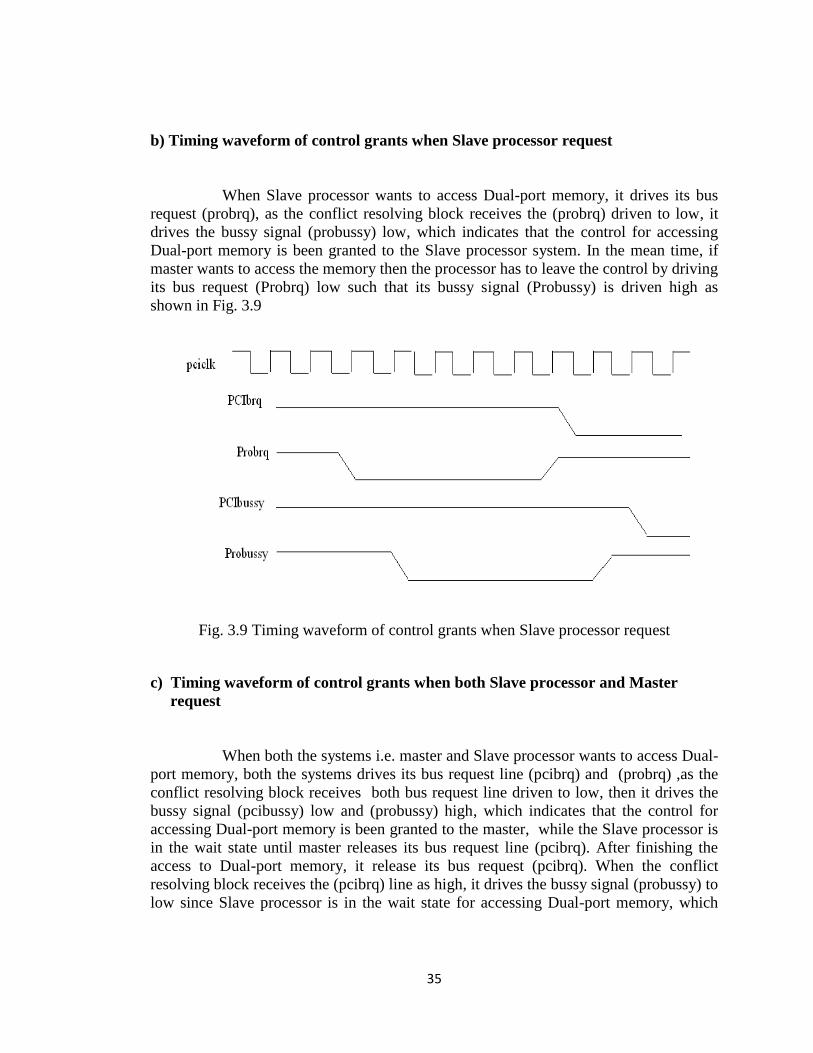
b) Timing waveform of control grants when Slave processor request
When Slave processor wants to access Dual-port memory, it drives its bus
request (probrq), as the conflict resolving block receives the (probrq) driven to low, it
drives the bussy signal (probussy) low, which indicates that the control for accessing
Dual-port memory is been granted to the Slave processor system. In the mean time, if
master wants to access the memory then the processor has to leave the control by driving
its bus request (Probrq) low such that its bussy signal (Probussy) is driven high as
shown in Fig. 3.9
Fig. 3.9 Timing waveform of control grants when Slave processor request
c) Timing waveform of control grants when both Slave processor and Master
request
When both the systems i.e. master and Slave processor wants to access Dual-
port memory, both the systems drives its bus request line (pcibrq) and (probrq) ,as the
conflict resolving block receives both bus request line driven to low, then it drives the
bussy signal (pcibussy) low and (probussy) high, which indicates that the control for
accessing Dual-port memory is been granted to the master, while the Slave processor is
in the wait state until master releases its bus request line (pcibrq). After finishing the
access to Dual-port memory, it release its bus request (pcibrq). When the conflict
resolving block receives the (pcibrq) line as high, it drives the bussy signal (probussy) to
low since Slave processor is in the wait state for accessing Dual-port memory, which

36
indicates that, the control now been transfer to the Slave processor for accessing Dual-
port memory as shown in Fig. 3.10
Fig. 3.10 Timing waveform of control grants when both Slave processor
and Master request
3.2.1.2 Device Utilization Summary Of The Conflict Resolving Block
The device utilization summary of the conflict resolving block implemented on the
Spartan-3 XC3S200 FPGA (200 K gates) is shown in table 3.3. It shows the number of
slices and other resources available utilized in implementing the design on FPGA.
Table 3.3 Device Utilization Summary Of The Conflict Resolving Block

37
3.2.2 Interactive Controller Block
The interactive controller block as shown in Fig. 3.11, generates valid signals
and maintains the Dual-port memory every time a write or read address on address lines
and data on data lines is generated by master and Slave processor. Control block
receives these signals and allows these signals to propagate to the memory block,
depending on the master processor bussy signal.
As in the previous section, we have seen that the conflict resolving block
drives the bussy line of the requesting system, also we seen that when both (master and
Slave Processor) request for the access , conflict resolving block drives the bussy line of
the master while keeping the Slave processor in a wait state until master processor
finishes its operation.
Fig. 3.11 Interactive Controller Block
When the master processor generates the address on address lines, data on
data lines and write/read signal, then the control block check for the bussy line of
master. When the control block receives the bussy line of master driven to low, it allows
the address on valid address lines, data on valid data lines and valid wr_rd signal to
38
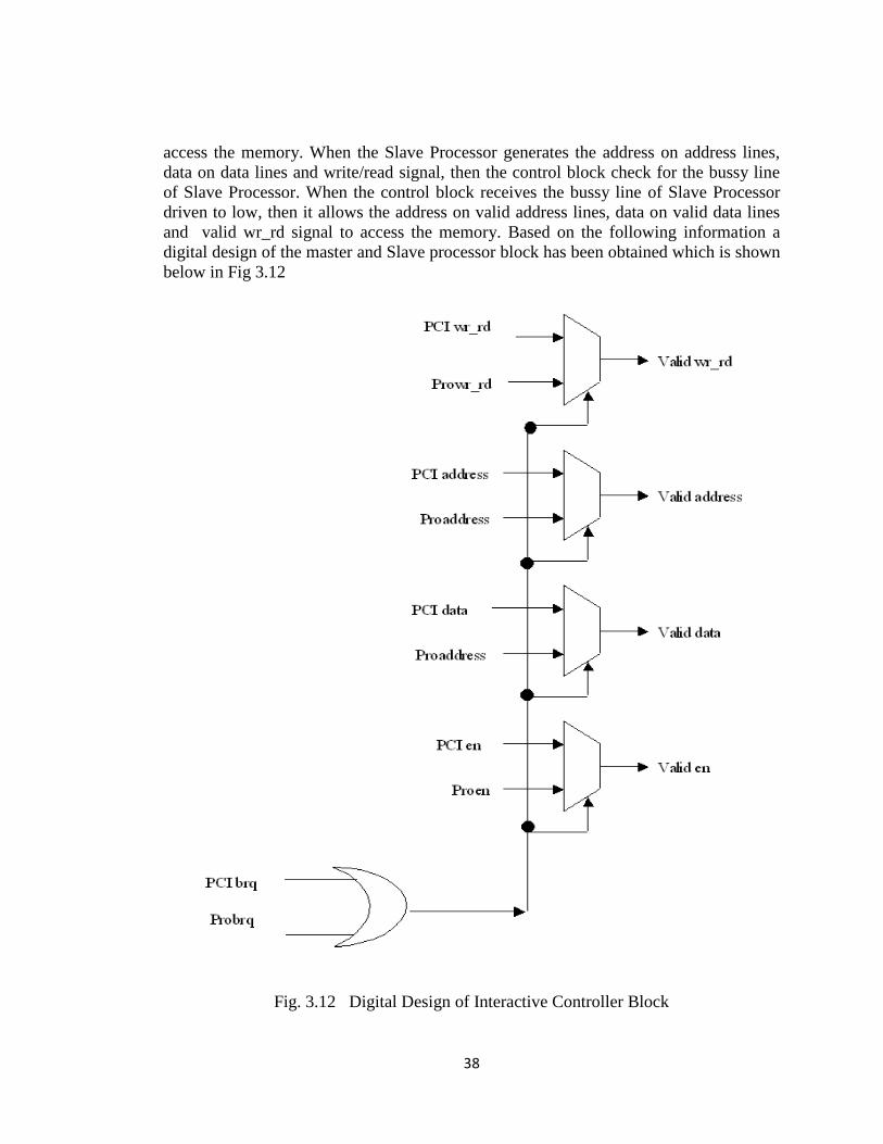
access the memory. When the Slave Processor generates the address on address lines,
data on data lines and write/read signal, then the control block check for the bussy line
of Slave Processor. When the control block receives the bussy line of Slave Processor
driven to low, then it allows the address on valid address lines, data on valid data lines
and valid wr_rd signal to access the memory. Based on the following information a
digital design of the master and Slave processor block has been obtained which is shown
below in Fig 3.12
Fig. 3.12 Digital Design of Interactive Controller Block

39
3.2.2.1 Timing waveforms And Its Description
The main function of the control block is to just select or decide whether the
master or Slave processor should access the memory at the given time, this block is
merely a combination of the conflict resolving block and the memory read and write
block. We have already seen the timing waveforms of the conflict resolving block in the
previous section, and the remaining memory read write timing waveforms we will
witness in the succeeding section.
3.2.2.2 Device Utilization Summary
The device utilization summary of the interactive Controller block
implemented on the Spartan-3 XC3S200 FPGA (200 K gates) is shown in table 3.4. As
this block is the combination of mainly the multiplexers. It shows the number of slices
and other resources utilized in implementing the design on FPGA.
Table 3.4 Device Utilization Summary Of The Interactive Controller Block
3.2.3 Memory block
The main purpose of this block is to fulfill the storage requirement of both
the Master and the Slave Processor. This storage core is a dual port memory of 64 k size,
fully synchronous such that the data is to be written on the rising edge of the clock. It is
the central block which depends on the output of all the blocks such that as soon as the
conflict resolving block will decide, whether Master or Slave Processor will access the

40
memory ,the controller block will send the valid signals for accessing the memory as shown
in Fig. 3.13
Fig. 3.13 Memory block and its Connectivity
3.2.3.1 Timing waveforms And Its Description
a) Single byte Write cycle
As it can be seen from the timing waveform shown in figure 3.14 that during
the beginning first clock cycle, the frame#,trdy# and irdy# signals are driven high and
address is being sent on the add data line and during the end of second clock cycle
,frame signal is driven low and the address is latched in the memory. During the
beginning of sixth clock cycle both the irdy# and trdy# signals are driven low and data is
being send on the add data line and during the beginning of ninth clock cycle, the
frame# signal is driven high and the PCI wr signal is driven low, such that the data is
written in memory as shown in Fig. 3.14

41
Fig. 3.14 Single byte Write cycle
b) Single byte Read cycle
As it can be seen from the timing waveform shown below that during the
rising edge of first clock cycle ,the frame# signal is driven high and during the second
clock cycle the irdy# and trdy# are driven high and during the sixth clock cycle ,the
frame# signal is driven low and the PCI wr signal is driven high ,so that the address can
be latched in the memory and the output corresponding to desired address can come on
the output line as shown in Fig. 3.15
Fig.3.15 Single byte Read cycle

42
3.2.3.2 Device utilization by memory block
The device utilization summary of the memory block implemented on the
Spartan-3 XC3S200 FPGA (200 K gates) is shown in Table no 3.5 It shows the number
of slices and other resources utilized in implementing the design on FPGA.
Table no. 3.5 Device utilization by memory block
3.3 Simulation Results
3.3.1 Master Continuous write and Slave continuous Read
. The master processor writes continuously from 00 to FF and the Slave processor reads
the data continuously from 00 to FF as shown in the Fig 3.16

43
Fig. 3.16 Master Continuous write and Slave Processor read continuous cycle
In this the Master processor takes the control from the conflict resolving
block by driving its bus request (pcirq) to access the memory. Then it broadcasts the
address and data on address_data line such that first the address is sent by driving
frame# as low and irdy# and trdy# high the address is latched , then the data is sent by
driving frame# high and driving irdy# and trdy# low the data is latched , in the mean
time the pciwr(Master write) signal is also made low such that the data is written in the
memory.

44
After the data is written in to the memory ,the data can be continuously read
by the Slave processor by just giving the address in the read address line and by
applying read clock ,in the mean time the pw(Slave write) signal should also be made
high so that the output data can appear on the Slave processor data (pd) output line.
3.3.2 Master Processor Write and Read cycle
In this, the master bus writes the data from 00 to FF and then reads it in the
similar fashion i.e. from 00 to FF. For this the master processor takes the control from
the conflict resolving block by driving its bus request (PCIrq) to access the memory.
Then it broadcasts the address and data on address_data line, such that first
the address is sent by driving frame# as low and irdy# and trdy# as high ,the address is
latched , then the data is sent by driving frame# high irdy# and trdy# as low ,the data is
latched , in the mean time the PCIwr signal is also made low such that the data is written
in the memory.
After the data is written in to the memory the data can be continuously read
by just giving the address in the same way on the address_data line and driving the
pciwr signal as high, such that the data will appear on the output line(pcida).
The simulation waveform of master processor write and read cycle is shown
in Fig 3.17. The main advantage of doing this is that microcontroller can use the
extended memory implemented on FPGA when needed.

45
Fig. 3.17 Master Processor Write and Read cycle
3.3.3 Slave Processor write and read cycle
In the similar fashion as discussed above, the Slave processor can writes the
data from 00 to FF and then reads it in the similar fashion i.e. from 00 to FF. In this the
processor take the control from the conflict resolving block by driving its bus request
(pr) to access the memory. Then it broadcasts the address on address lines (pa [0:7]) and
data on data lines (pd [0:7]), then it drives its write/read signal (pw) to low, after that it

46
drives its chip enable signal (pe) to low, which causes the data to be written to memory
of the specified address.
For reading the data from memory the processor broadcasts the address on
address lines (pa [0:7]) then it drives its write/read signal (pw) to high after that it drives
its enable signal (pe) to low, which causes the data to be read from the memory
corresponding to the specified address.. The whole simulation waveform is depicted in
Fig. 3.18
Fig. 3.18 Slave Processor write and read cycle

47
3.4 Testing of Priority based architecture sharing data with Microcontrollers in
Real Time
The data sharing architecture is tested in real time environment by interfacing
with two AVR AT90S8515 micro controllers in which one acts as Master, which is
inter-faced to the PORTB of the controller and the other acts as Slave processor, which
is interfaced to the PORTA of the controller. The AVR used in the place of Master
generates the exact signals of PCI, but the operation is slow as compared to the original
PCI card. However the testing is perform on the basis of PCI specification timing
diagram [6]. The other AVR (Slave) interfaced to PORTA of the controller
communicates with the AVR (Master) interfaced to the PORTB of the controller.
The AVR acting as Master and Slave respectively generates the address via
PORTA, data via PORTD and the control signals via PORTB, as shown in Figure 3.19
below
Fig. 3.19 Testing of Priority based architecture sharing data with Microcontrollers
in Real Time

48
3.4.1 Testing of Slave Processor in Real Time
One of AVR acting as the Slave processor generates the exact signals of the
Slave processor through the AVR pins as shown in the Table no.3.6 .The whole
operation is started with the event when the Probrq signal is set to low via PORTB of
AVR which is interfaced to the left of the FPGA, then a check has to be done for
Probussy signal ,whether it is low or high. If it is high ,then the processor will go in wait
state, if not ,then the processor will generate 8-bit address via PORTA of AVR and
drives the Prowr_rd signal to low via PORTB of AVR, which indicates to the
architecture implemented in FPGA that the operation to be performed is write operation,
if Prowr_rd signal is driven high, then it indicates Read operation.
If the operation to be performed is write, then the Slave processor generates
the 8-bit data via PORTD of AVR and then drives the Proen signal to low via PORTB
and wait until the Proack signal of PORTB goes to low. When the Proack signal is low
,then the processor drives the Proen to high again , if this is the last cycle then it stops
the operation, else the address and data is incremented from 00-FF. and the whole
process is repeated for each increment of address and data. Once the address and data
reaches the value of FF the process get stop.
Table no. 3.6 Pin Description for Testing of Slave Processor in Real Time

49
If the operation to be performed is read, then the Slave processor drives the
Proen signal via PORTB of AVR and waits for the Proack to go low. When the Proack
signal is low, the data is displayed on the LEDs via PORTC of AVR. (Since the data bus
is bidirectional the data is copied to PORTC from PORTD and displayed on 8 LED’s of
AVR) Then the Slave processor drives the Proen to high again, and If cycle is last then it
stops operation, else the address is incremented from 00 to FF, and the whole process of
read is repeated for each increment of address. Once the address reaches the value of FF,
the process stops. The read/write operation is also depicted in the flow chart shown in
Fig. 3.20 and Fig. 3.21
.
Fig. 3.20 Slave Processor Read Operation

50

51
Fig. 3.21 Slave Processor Write Operation
Increment the data

52
3.4.2Testing of Master Processor in Real Time
The other AVR acting as the Master processor generates the exact signals of
the Master processor through the AVR pins as shown in the Table no. 3.7
The whole process started with the event when the PCI brq signal is set to
low via PORTB of AVR, which is interfaced to the right of the FPGA, and then wait for
probussy signal to go low. When the PCIbussy signal is low, then the Master will
generate 8-bit address via PORTA of AVR, in order to latch the address it drives the PCI
frame# signal low and irdy# and trdy# high through PORTB. After that the data is being
sent on the address data line, in order to latch the data the frame# signal is driven high
and the irdy# and trdy# are driven low. As the operation to be performed is write, so the
read/write signal is driven through PORTC, the PCI en signal is also driven low so that
the data ack signal is also get low and which is a input to PORTC and If the cycle is last
then it stops operation, else the address and data is incremented from 00-FF.and the
whole process repeated for each increment of address and data. Once the address and
data reaches the value of FF the process stops. The pin description is shown in table 3.7
Table no. 3.7 Pin Description for Testing of Slave Processor in Real Time

53
1. If the operation to be performed is read then the PCI drives the read/write signal to
high via PORTC of AVR and then waits for the PCI dtack to go low. When the PCI
dtack signal is low, the data is displayed on the LEDs (Since the output data bus is
directly got connected to AVR LEDs). If the cycle is last then the process is stopped
2. Else the address is incremented from00-FF. and the whole process of read is repeated
for each increment of address. Once the address reaches the value of FF the process
stops. The whole read/write operation is depicted in the flow chart in Fig 3.22 and
3.23

54

55

56
Fig. 3.22 Master Processor Write Operation

57
Fig. 3.23 Master Processor Read Operation

58
3.4.3 Testing Results
The whole testing setup having FPGA Spartan3 Kit acting as our Data sharing
architecture and AVR90S8515 microcontrollers acting as Master and Slave respectively,
is depicted in Figure 3.24 and Testing results are discussed under the following points:
1.Continuous write and read test: - Data is written via PORTB continuously from 00
to FF in increasing order and the data is read continuously via PORTA and displayed on
the LED’s of the AVR AT90S8515 kit. It is observed that data is read in the same order
as it is written in memory by Master.
2.Master Processor write and read test: - Data is written via PORTA from 00 to FF in
increasing order. Then the data is read via LED’s connected to AVR kits. It is observed
that data is read in the same order as it is written in memory by Master.
3.Slave Processor write and read test: - Data is written via PORTA from 00 to FF in
increasing order. Then the data is read via LED’s connected to AVR AT90S8515 kit. It
is observed that data is read in the same order as it is written in memory by Slave
processor.
4.Master Processor write and Slave Processor read test: - Data is written via PORTA
from 00 to FF in increasing order. Then the data is read via PORTA and displayed on
LED’s connected to AVR AT90S8515 kit. It is observed that data is read in the same
order as it is written in memory by Master.
5. Slave Processor write and Master Processor read test: - Data is written via
PORTA from 00 to FF in increasing order. Then the data is read via PORTB and
displayed on LED’s connected to AVR AT90S8515 kit. It is observed that data is read
in the same order as it is written in memory by Master Processor.

59
Fig. 3.24 Testing Setup