chapter 4 introduction to...
TRANSCRIPT

91
CHAPTER 4 NANOINDENTATION OF ZR BY MOLECULAR DYNAMICS SIMULATION
Introduction to Nanoindentation
In Chapter 3, simulations under tension are carried out on polycrystalline Zr. In
this chapter, nanoindentation is going to be used as the tool to study the deformation
mechanism of single crystal Zr with different surface orientations. Nanoindentation is
now an important and widely-used method used to probe the mechanical properties of
materials at the nanoscale. In particular, it is commonly used for measuring basic
mechanical properties such as hardness and elastic modulus 145. With further
development, other mechanical properties can also be determined using
nanoindentation 146, 147. To observe the nucleation and propagation of dislocations and
evolution of defect structures, nanoindentation has been combined with electron
microscopy to characterize deformation processes at the nanoscale in real time. Nili et
al. have discussed the application and development of in situ nanoindentation
technology to several different materials systems 148; opportunities and challenges of in
situ nanoindentation and scratch testing combined with SEM have also been reviewed
149. Despite the development of in situ nanoindentation, full observation of the
nucleation and propagation of dislocations at the atomic level remains challenging.
Molecular dynamics (MD) simulation has been used as an effective tool to study
the deformation process of metals 20-22, 24, 28, 150 at the atomic level. For example, Van
Swygenhoven and coworkers have shown that the stable and unstable stacking fault
energies have a strong influence on deformation behavior in fcc metals24. Work on Zr by
The work in this Chapter has been published in Z. Z. Lu, M. J. Noordhoek, A. Chernatynskiy, S. B. Sinnott and S. R. Phillpot,
Journal of Nuclear Materials, 2015, 467, 742.

92
Lu using polycrystalline models discussed the relationship between deformation
behaviors and the stable and unstable stacking fault energies 150. The nanoindentation
process has been studied using MD in fcc 151-154, bcc 155, 156 and hcp 157 metals. Indeed,
computational methods have played a very important role in elucidating the atomic-level
mechanisms of dislocation nucleation and propagation under nanoindentation 146.
In this chapter, we perform MD simulations of nanoindentation of a Zr single
crystal. Two different empirical potentials are used in the simulation: a Charge
Optimized Many Body (COMB) potential 132 and the Mendelev and Ackland Embedded
Atom Method (MA EAM) potential 103. The details of the above two potentials are
introduced in the interatomic section of Chapter 2. And the simulation results of 2D
textured models and 3D models under tensile condition using the above two potential
are analyzed in Chapter 3. The nucleation and propagation of dislocations are analyzed
from the atomistic point view. The effects of four different surface orientations are
discussed. The influence of stable and unstable stacking energies on deformation
behavior is revealed from the comparison of the results of the two potentials. In future
work, we will use the extension of the COMB potential to the Zr-H-O system 71 to
analyze the effects of oxidation and hydriding on the deformation behavior under
nanoindentation, and the hardness of Zr.
Simulation Setup
The LAMMPS MD simulator is used to perform the nanoindentation simulations
158. The simulation system consists of an active region, a thermostat region and a fixed
region, as shown in Figure 4-1. The active region interacts with the indenter and the
movement of atoms in this region is governed purely by the forces on them, with no
constraints. The thermostat region helps to control the temperature of the whole system;

93
a Langevin thermostat 83 is applied to this region to control the system’s temperature.
The fixed region is used to provide rigid support. Periodic boundary conditions are
applied in the plane of the Zr film (x and y directions). Prior to the nanoindentation
simulation itself, the system is equilibrated under NPT condition at 300K for 50ps. As
shown in Figure 4-1, the rigid spherical indenter interacts with the active region. The
indentation simulation is performed using the “fix indent” command built in LAMMPS.
The force exerted by the spherical indenter on each atom in the Zr film is described by:
F(r) = - K(r – R)2 r < R (4-1)
F(r) = 0 r ≥ R (4-2)
Here, K = 10 eV/Å3 is the force constant for interactions between the indenter and
the film, r is the distance from the atom to the center of the indenter and R (=45Å) is the
radius of the indenter.
Regarding the use of a spherical indenter, the simulation results in the elastic
region can be easily compared with the classical Hertz Law. However, stress
concentration at a sharper indenter tip could lead to stronger stress concentration and
thus lower the stress needed for the first plastic event; for example, when using conical
indenters, the both experiment and numerical results show that the hardness increases
as the corner angle decreases 159. For the spherical indenter, the hardness depends on
the radius of the indenter rather than the indentation depth; the hardness increases as
the indenter size decreases 160. Using the spherical indenter allows us to determine the
hardness. In addition, the weaker stress concentration for spherical indenter can reduce
the dislocation pile up, making it easier to analyze the individual dislocation behaviors.

94
Hertz Law
The load-displacement curves are extracted from the indentation simulation.
Prior to the first plastic event, the load-displacement curve shows the characteristic
features of elastic response. Hertz continuum elastic contact analysis has been used to
determine the elastic deformation behaviors for spherical indenter. Within Hertz theory
161, 162,
� =�
��∗�
�
�ℎ�
� (4-3)
where P is the applied load by the indenter, R is the radius of curvature of the
indenter, h is the indentation depth, and �∗ is the reduced modulus, defined as 161, 162,
�∗ = �����
�
��+
�����
���
��
(4-4)
where Es and νs are Young’s modulus and Poisson’s ratio of the sample and Ei
and νi are Young’s modulus and Poisson’s ratio of the indenter. For the hard indenter
E=∾ and =0.
The Young’s modulus E under a uniaxial stress �[�����],�[�����],and �[����] is
described in terms of components of the compliance tensor S 163-166,
�[�����] = (���)�� (4-5)
�[�����] = (���)�� (4-6)
�[����] = (���)�� (4-7)
���° �����������= (����)�� (4-8)
���� = ��� ∙ ����(30°) + ��� ∙ ����(30°)
+ (2��� + ���) ∙ ����(30°) ∙ ����(30°) (4-9)

95
Under a uniaxial stress �[�����],�[�����],and �[����], the average Poisson’s ratio can
be expressed as 163-166,
�[�����] =�(�������)
���� (4-10)
�[�����] =�(�������)
���� (4-11)
�[����] =�(�������)
���� (4-12)
���° ������� =�����
� ����� �
����� (4-13)
���� = ��� ∙ [����(30°) + ����(30°)]
+ (��� + ��� − ���) ∙ ����(30°) ∙ ����(30°) (4-14)
The relationship between stiffness C and compliance S is 166, 167,
��� + ��� =���
�� (4-15)
��� − ��� =�
������� (4-16)
��� =����
�� (4-17)
��� =�������
�� (4-18)
��� =�
��� (4-19)
�� = ���(��� + ���) − 2���� (4-20)
Through Equation 4-4 to Equation 4-20, the reduced modulus �∗ of MA EAM and
COMB potentials can be obtained, as shown in Table 4-1.
Hardness Calculation Method
The hardness, H, can also be extracted from the nanoindentation 168,
H=P/A (4-21)

96
Where P is the load in the direction perpendicular to the surface of the indenter
and A is the imprinted area of the indenter on the surface. Equation 4-21 will be used to
calculate the hardness value of the nanoindentation simulation. The load value P is
calculated directly from the simulation by the LAMMPS code. The area A is calculated
using
A=πδ(2R - δ) (4-22)
Where R is the radius of the indenter and δ is the indentation depth.
The method used to calculate hardness is shown in Figure 4-2. In the elastic
region, hardness as defined in Equation 4-21 is a strong function of the indentation
depth, but once the plastic deformation begins, its value stabilizes and only fluctuates
slightly, reflecting the various operant deformation processes. This is illustrated in the
relationship between hardness and indentation depth in Figure 4-3. The hardness is
thus obtained by calculating the instantaneous simulated values of the hardness over
the indentation depths greater than about 9Å shown in the red dot line region in Figure
4-3. The hardness data in Figure 4-3 is sampled apart of 100fs, one phonon period. The
reported hardness is the mean value. The reported error bars of the hardness are
represented by the standard deviation from the average in this dataset.
Indentation Speed
In indentation experiments, the velocity of the indenter ranges from tens of
nm s-1, to 1 mms-1, 157. Because of the computational cost of MD simulation, the velocity
of the indenter has to be of the order of ms-1, which is much faster than experiment. In
order to explore the effect of the indentation speed on the nanoindentation results,
simulations were performed under different indenter velocities, ranging from 2 ms-1 to
50 ms-1. Because simulations using the MA EAM potential are less time consuming

97
than simulations with the COMB potential, this indentation speed test is performed using
only the MA EAM potential and the [0001] orientation. A relatively small system size is
used to perform the indentation speed test.
From Figure 4-4, we can see that while the general shape and characteristics of
the load-displacement curve are only weakly dependent on the indentation speed, the
fine details are substantially different, especially for the fastest nanoindentation
simulation of 50 ms-1. These fine details are associated with the various dislocation
nucleation and propagation processes, as we describe in detail below. In particular, the
first peak in the load map before it drops takes place at the indentation depth of ~5 Å for
2, 5, 10 and 25 ms-1 speeds, but at somewhat deeper indentation depth for 50 ms-1. In
addition, the magnitude of this first load drop generally increases as the indentation
speed decreases, with the 2, 5, and 10 ms-1 drops being very similar. Similarly, the 2nd
and subsequent peaks on the load-displacement curves for 2, 5, 10, 25 and 50 ms-1 are
all at different indentation depths. Overall, for slower speeds, there are more peaks and
the load drop for each peak is larger. Detailed comparison of the processes, however,
which is presented in Figure 4-5 for 5 and 50 ms-1, clearly demonstrates that faster
speed results in qualitatively different behavior; namely there are very few dislocation
loops observed for 50 ms-1, while they are present in all simulation with slower
indentation speeds. For faster indentation speed, pyramidal dislocations mainly form,
while for slower indentation speed, pyramidal, basal and prismatic dislocations all form.
The hardness obtained from different indentation speeds also varies systematically:
4.5±0.2 GPa (50 ms-1), 4.2±0.2 GPa (25 ms-1), 4.0±0.2 GPa (10 ms-1), 3.6±0.3 GPa (5
ms-1) and 3.5±0.26 GPa (2 ms-1). As the indentation speed decreases, the calculated

98
hardness becomes smaller, becoming essentially independent of indentation speed at
low speeds. Subsequent simulations use 5 ms-1 as the indentation speed as providing a
realistic representation of the dislocation behaviors in Zr at a reasonable computational
load.
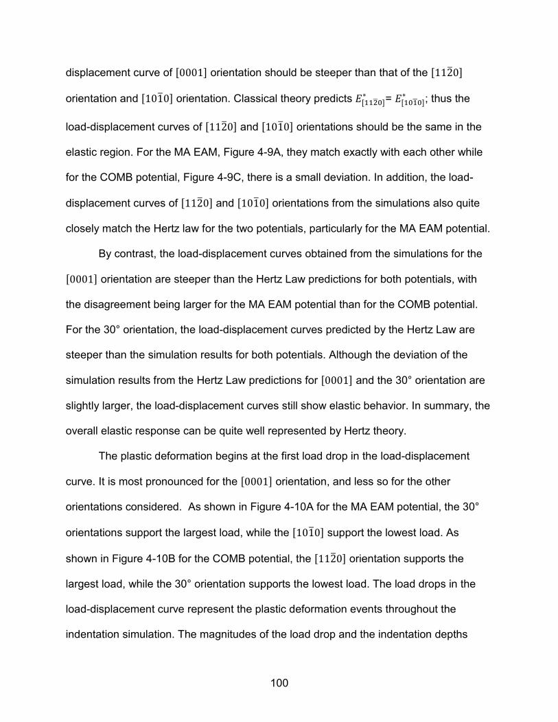
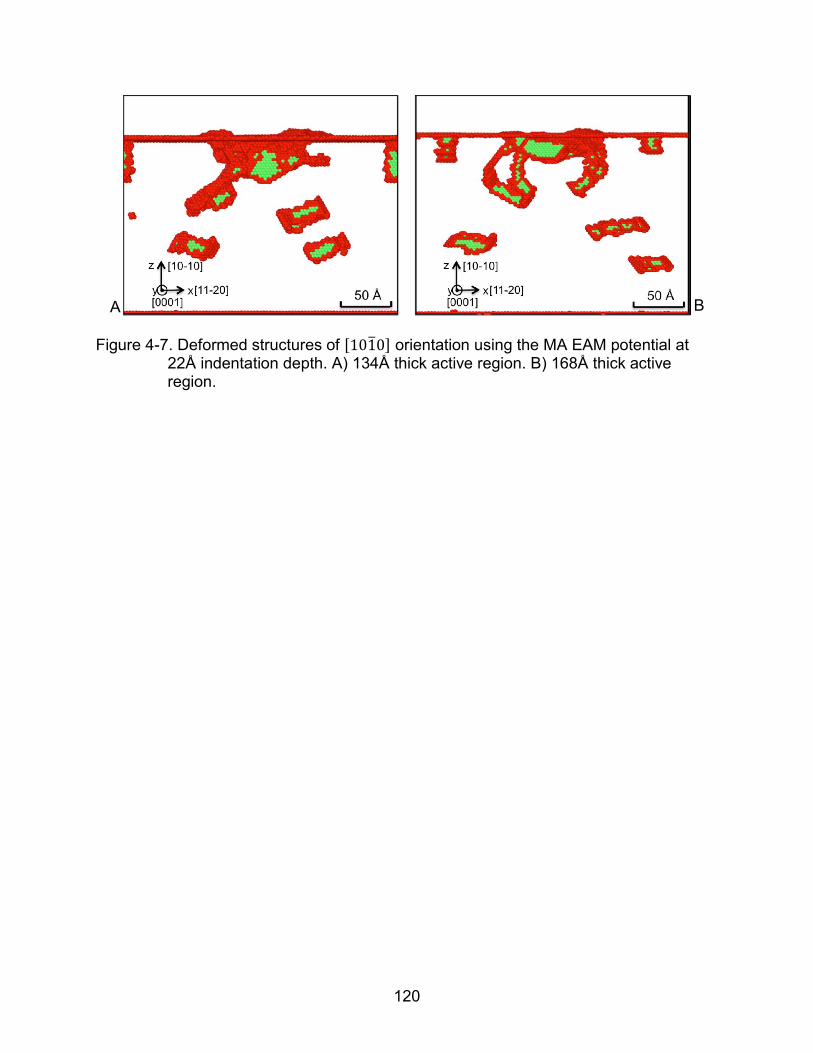
Substrate Thickness Effect
Systems used in MD simulations have dimensions of tens or at most a few
hundred nanometers. The characteristics of the load-displacement curve can be
influenced by the system size. In order to understand how the substrate’s thickness
influences the load-displacement curve in both elastic deformation and plastic
deformation regime, MD nanoindentation simulations with different active layer sizes are
tested for the [101�0] orientation, using the MA EAM potential. It can be seen from
Figure 4-6 that the thickness of the active layer has an effect on the load-displacement
curve for small thicknesses of the active layer, converging for larger thicknesses, with
the results for 168 Å and 190 Å being essentially identical. Further evidence that this
system size is adequate come from the fact that the slope of the load-displacement
curve matches the Hertz law result. For thicker active layer as shown in Figure 4-6, the
first load drop related to the plastic deformation takes place at a smaller indentation
depth. As for the characteristics of the dislocations, there are no fundamental structural
differences for different active layer thickness, as shown in Figure 4-7. The dislocation
loop travels downwards and stops at the bottom of the active region. The strain field of
the dislocation loop is different for different thickness active region; in particular, the
dislocation loops in the thicker active region are larger in size. As for simulations with
the COMB potential, no dislocation loops have been observed, so the substrate
thickness effect is smaller for COMB than MA EAM.

99
Indentation with Different Orientations
In indentation of a single crystal, the crystallographic orientation of the indented
surface will promote some deformation modes and hinder others, thus eliciting different
mechanical responses 33. Murty and Charit performed a detailed experimental study of
the orientation development and deformation behavior in zircaloys 42. In this work, four
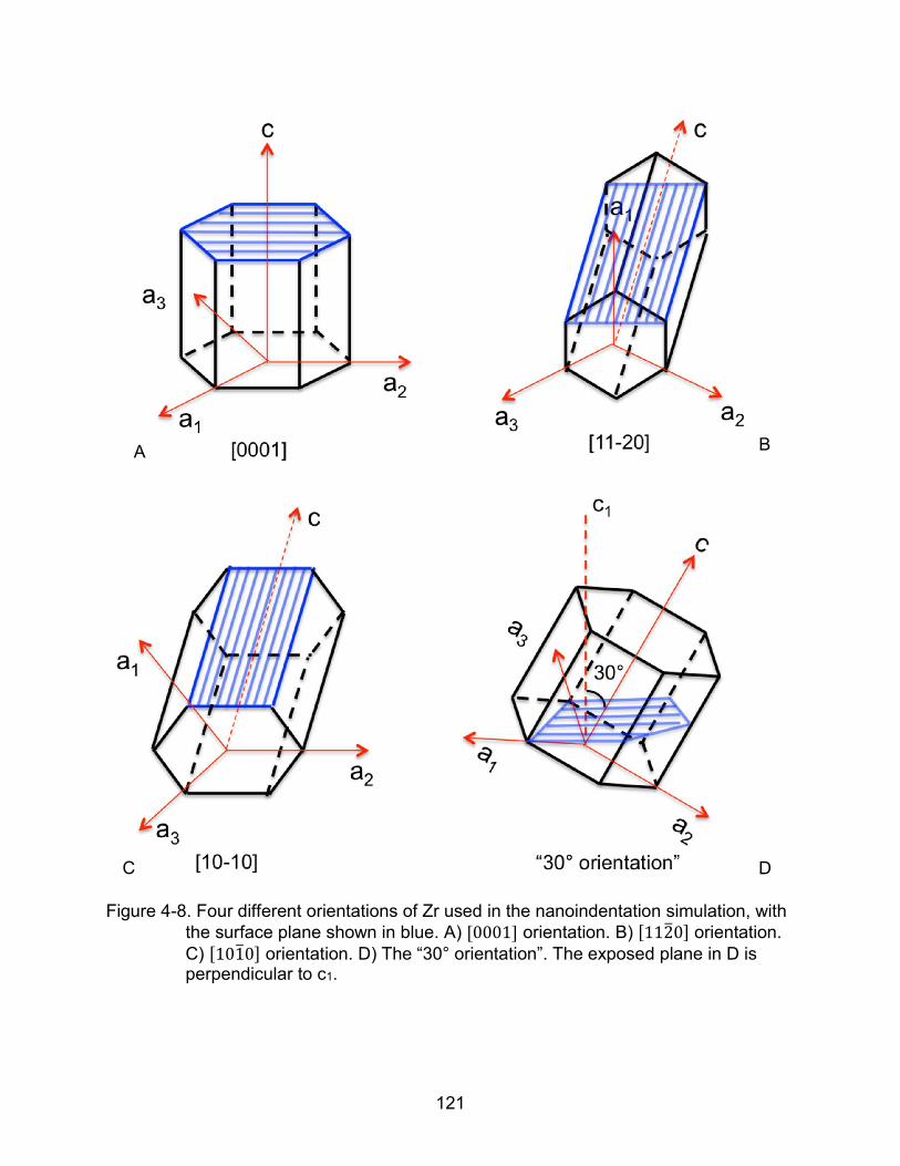
different orientations as shown in Figure 4-8 are chosen to perform the indentation
tests: [0001], [112�0], [101�0] and the [0001] orientation rotated by 30° around the c-axis
(“the 30° orientation”), commonly used in zircaloy 42. From the crystallography point of
view, the [112�0] and [101�0] orientations promote prismatic <a> slip and basal <a> slip.
The [0001] orientation promotes pyramidal <a+c> slip. The 30° orientation promotes
pyramidal <a+c> slip and basal <a> slip. The load-displacement curves for the two
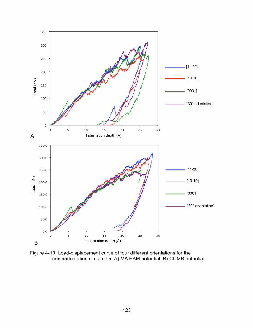
potentials in the elastic region are shown in Figure 4-9, while complete load-
displacement curves are shown in Figure 4-10. The hardness values calculated from
these data are shown in Figure 4-11. The hardness value is obtained from experiment
done on Zr-1Nb-0.05Cu zirconium alloy 169. The polycrystalline zirconium alloy has
more different grain boundary structures and more different grain orientations, which
can make it easier for dislocations to nucleate. So it is reasonable that the hardness
value of the tested zirconium alloy is smaller than that of the simulation results.
Before the first dislocation activity, the characteristic of the load-displacement
curve lies in the elastic regime. The MD results are consistent with the Hertz analysis; in
particular, in the elastic regions shown in Figure 4-9, the load does indeed vary as h3/2
for both potentials and for all four surface orientations; the reduced modulus values, �∗
arHe shown in Table 4-1. These E* values indicate that the slope of the load-
100
displacement curve of [0001] orientation should be steeper than that of the [112�0]
orientation and [101�0] orientation. Classical theory predicts �[�����]∗ = �[�����]
∗ ; thus the
load-displacement curves of [112�0] and [101�0] orientations should be the same in the
elastic region. For the MA EAM, Figure 4-9A, they match exactly with each other while
for the COMB potential, Figure 4-9C, there is a small deviation. In addition, the load-
displacement curves of [112�0] and [101�0] orientations from the simulations also quite
closely match the Hertz law for the two potentials, particularly for the MA EAM potential.
By contrast, the load-displacement curves obtained from the simulations for the
[0001] orientation are steeper than the Hertz Law predictions for both potentials, with
the disagreement being larger for the MA EAM potential than for the COMB potential.
For the 30° orientation, the load-displacement curves predicted by the Hertz Law are
steeper than the simulation results for both potentials. Although the deviation of the
simulation results from the Hertz Law predictions for [0001] and the 30° orientation are
slightly larger, the load-displacement curves still show elastic behavior. In summary, the
overall elastic response can be quite well represented by Hertz theory.
The plastic deformation begins at the first load drop in the load-displacement
curve. It is most pronounced for the [0001] orientation, and less so for the other
orientations considered. As shown in Figure 4-10A for the MA EAM potential, the 30°
orientations support the largest load, while the [101�0] support the lowest load. As
shown in Figure 4-10B for the COMB potential, the [112�0] orientation supports the
largest load, while the 30° orientation supports the lowest load. The load drops in the
load-displacement curve represent the plastic deformation events throughout the
indentation simulation. The magnitudes of the load drop and the indentation depths

101
where the load drop happens all vary slightly for different orientations of different
potentials. One obvious similarity for both potentials is that the [0001] orientation has
the largest first load drop at around 5 Å indentation depth. The details of the plastic
deformation events are discussed later.
The comparison of hardness for the four simulated orientations of two potentials
is shown in Figure 4-11. The 30° orientation (MA EAM) and [112�0] orientation (COMB)
have highest hardness value, while the [101�0] orientation (MA EAM) and the 30°
orientation (COMB) have the lowest. However, as shown in Figure 4-3, the hardness
fluctuates with the indention depth. So when taking into account the fluctuations
represented by the errors bars in Figure 4-11, the difference of the hardness value for
different orientations of the two potentials is not significant.
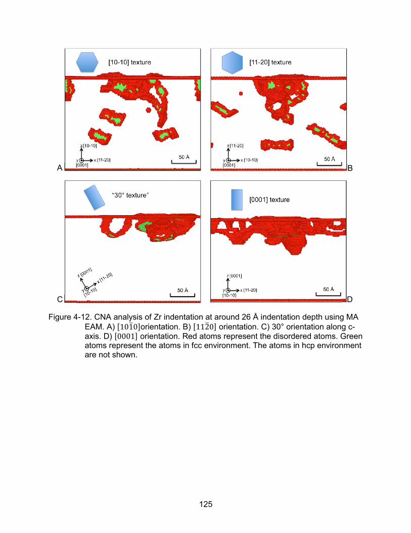
The atomic-level details of the deformed structures combined with the elastic
properties provide insights into these differences in the hardness and load-displacement
curves. The deformed atomic structures of the four orientations are shown in Figure 4-
12 (MA EAM) and Figure 4-13 (COMB) where again atoms are color coded in accord
with Common Neighbor Analysis (CNA) 126, 127. The calculated total dislocation line
length, dislocation segments and junctions of all the deformed structure using the
Crystal Analysis Tool are listed in Table 4-2 123-125. The Crystal Analysis Tool has some
difficulties in capturing the dislocation structure in the COMB simulations. So the
dislocation density of the COMB simulations is not listed in Table 4-2.
MA EAM Indentation Analysis
From the deformed structures of four different orientations shown in Figure 4-12,
we can see that dislocation loops are commonly activated for the MA EAM potential.

102
The dislocation loop consists of partial dislocations on the basal plane and dislocations
on the prismatic planes. Dislocation loops are only observed traveling along the <a>
direction on prismatic plane inside the bulk or on the surface in this nanoindentation
simulation. The dislocation loop observed in this nanoindentation turns out to be the
most stable interstitial loop in Zr, and has been observed by de Diego and coworkers in
their simulation work 170. They found that the rectangular self-interstitial loop that
consists of prismatic dislocations and basal partial dislocations has the lowest formation
energy and highest binding energy 170.
For the [101�0] and [112�0] orientations, as shown in Figures 4-12A and 4-12B,
the dislocation loops form under the indenter and travel along the <a> direction on the
prismatic plane. Despite their similar dislocation behaviors, there is a difference of
hardness between the [112�0] orientation (5.27 GPa) vs. [101�0] orientation (4.65 GPa).
When considering the elastic deformation contribution, as discussed in the previous
section the [112�0] orientation and [101�0] orientation have similar load-displacement
curves due to the same reduced modulus. With regards to the plastic deformation
contribution, the Schmid factors 171 for prismatic and basal slips are identical for these
two orientations: 0.433 (prismatic planes neither parallel nor perpendicular to the
indentation direction) and 0 (prismatic planes parallel or perpendicular to the indentation
direction) for prismatic slips and 0 for basal slip. However, for the [101�0] orientation,
the surface is one of the prismatic planes; therefore dislocation loops travelling along
the <a> direction on the surface are commonly observed in these nanoindentation
simulations. This dislocation loop motion on the surface may contribute to the lower
hardness for the [101�0] orientation. In addition, the size and the detailed atomic

103
structures of dislocations are different for these two orientations, with the dislocation
loops formed in the [112�0] orientation being generally larger. The detailed atomic
structures of one of the dislocation loops from each orientation are shown in Figure 4-
14. The sizes of the dislocation loop for [101�0] and [112�0] orientations are 42Å55Å
and 66Å55Å correspondingly. The basal partial component of the dislocation loop is
longer for [112�0] (66 Å) than for [101�0] (42 Å). In addition, more jogs are formed in the
basal partial component of the dislocation loop for the [112�0] orientation than for the
[101�0] orientation. From the dislocation structures we conclude that more plasticity
events take place in the [112�0] orientation than in the [101�0] orientation. This is
confirmed by the calculation results from the Crystal Analysis Tool: the [112�0]
orientation yields longer total dislocation line length (1608 Å vs. 1315 Å for [101�0]),
more segments (72 vs. 51) and more junctions (36 vs. 23). From the load-displacement
curve, we can see that for the [101�0] orientation the large load drops happen at an early
stage of the plastic deformation, while for [112�0] orientation the large load drops
happen at a later stage of the plastic deformation. After 15 Å indentation depth, the load
response for [112�0] orientation becomes obviously larger than for the [101�0]
orientation. This leads to the result that the hardness of [112�0] (5.27 GPa) is higher
than that of [101�0] orientation (4.65 GPa). However, when taking into account the
uncertainties associated with the fluctuations shown in Figure 4-3 and Figure 4-11,
these values do not differ significantly. In summary, taking into account both of the
contribution from elastic and plastic deformation, the [112�0] orientation yields similar
hardness as [101�0] orientation does.

104
For the 30° and [0001] orientations, as shown in Figures 4-12C and 4-12D,
dislocation loops form under the indenter. For both orientations, the dislocation loops
only travel along the surface. The second basal partial dislocation cannot nucleate to
form a full dislocation loop. It is thus not surprising that dislocation loops are not
observed to leave the surface to travel inside the bulk. Pyramidal slip is observed along
with the dislocation loops.
Considering the elastic deformation, the reduced modulus of the [0001]
orientation has the highest value among the four orientations. The reduced modulus of
the 30° orientation (129 GPa) lies between those of the [0001] orientation (133 GPa)
and [112�0] orientation (114 GPa) but very close to [0001] orientation. Thus, from the
viewpoint of elasticity, the [0001] orientation should have the highest load response and
the steepest slope of the load-displacement curve in the elastic region, which agrees
with the simulation results as shown in Figure 4-10A.
Comparing the details of the plastic deformation of these two orientations may
give some insights to the difference in the magnitude of the load drop. As shown in
Figures 4-12C and 4-12D, the dislocation density is much higher for the [0001]
orientation than for the 30° orientation. In addition, the calculations from the Crystal
Analysis Tool show that the [0001] orientation has a total length of dislocation of 1132 Å
compared to 765 Å for the 30° orientation, confirming that the 30° orientation has the
lowest dislocation density. This lower dislocation density is consistent with the small
load drop. The small dislocation density combined with the moderately reduced
modulus results in the largest hardness value (5.68 GPa) for the 30° orientation among
the four orientations. Although it has the largest reduced modulus, the [0001] orientation
105
has a hardness of only 5.13 GPa due to the relative ease with which plastic events are
nucleated. Furthermore, this ease of nucleation for [0001] orientation is consistent with
the crystallography: the dislocation loop glides in the <a> direction on prismatic plane,
which is parallel to the surface for the [0001] orientation.
COMB Indentation Analysis
As we saw in Figure 4-11, the hardness values predicted from the COMB
potential are similar to those predicted from the MA EAM potentials. Nevertheless, as
we now discuss, the atomic-level details of the plastic response are somewhat different.
The deformed structures of four orientations are shown in Figure 4-13 for the
COMB potential. The prismatic <a> and pyramidal dislocation are the most prevalent;
moreover, there are very few basal partial dislocations. In the absence of basal partial
dislocations, the dislocation loop of basal and prismatic dislocations seen in MA EAM
simulation is not observed in the COMB simulation. The reasons for this difference will
be discussed in the following section.
For the [101�0] and [112�0] orientations, as shown in Figures 13 (a) and (b),
prismatic <a> dislocations and pyramidal dislocations are most commonly activated
during the indentation test. In the elastic deformation regime, the [101�0] and [112�0]
orientations yield very similar load-displacement curves because they have same
reduced moduli. In combination with their similar dislocation behaviors, this results in
similar hardness values, 5.37 GPa for the [101�0] orientation and 5.46 GPa for the
[112�0] orientation.
For the 30° and [0001] orientations, as shown in Figures 4-13C and 4-13D,
pyramidal <a+c> dislocations predominate. For the [0001] orientation, the load-

106
displacement curve has the highest load response in the elastic regime, as shown in
Figure 4-10B. Moreover, as in the case of the MA EAM potential, the load drop related
to the first plastic event, at around 5 Å indentation depth, is the largest among the four
orientations. The largest elastic deformation combined with the largest load drop leads
to a moderate hardness value of 5.04 GPa, smaller than that of [112�0] and [101�0]
orientations. For the 30° orientation, as a result of the smallest reduced modulus (121
GPa) among the four orientations, it has the lowest load response in the elastic regime,
as shown in Figure 4-10B. The dislocation behavior of the 30° orientation is very similar
to the [0001] orientation. With the contributions from both elastic and plastic
deformation, the 30° orientation yields the smallest hardness value of 4.79 GPa.
Comparison between MA EAM and COMB Potentials
In the elastic regime, both the MA EAM and COMB potential agree with the Hertz
Law predictions especially for the order of the load response of four different
orientations. In the plastic regime, the prismatic <a> dislocation and pyramidal
dislocation are most commonly observed for both potentials. Among the four
orientations, the [0001] orientation has the largest first load drop for both potentials,
which has a significant influence on the hardness value. And as we saw in Figure 4-11,
the hardness values predicted from the COMB potential are similar to those predicted
from the MA EAM potentials when taking into account the uncertainties represented by
the error bars. Nevertheless, the atomic-level details of the plastic response are
different. In contrast with the MA EAM potentials, no dislocation loops are emitted for
the COMB potential. The reason for this difference is discussed as below.

107
As is well known, the stacking fault and unstable stacking fault energies play an
important role in determining the dislocation behaviors 24. A comparison of the stacking
fault energies of MA EAM potential and COMB potential was reported previously 150.
Summarizing these previously reported results, the stable and unstable stacking fault
energies along the basal partial <a> path for the COMB potential are higher than for the
MA EAM potential, while the most reliable DFT values are the lowest. This explains why
basal partial dislocations and stacking fault structures are rare in COMB; in this regard
the MA EAM potential should have higher materials fidelity that the COMB potential.
Also the ratio of energy barriers for basal slip and prismatic slip, ������
����������, is 1.13 for MA
EAM and 1.41 for COMB potential, while the DFT 137 value is 1.26. That is, for the MA
EAM potential prismatic dislocations should be only slightly more prevalent than basal
partial dislocations. This is consistent with the dislocation loop consisting of basal partial
dislocations and prismatic dislocations being commonly observed for MA EAM potential.
By contrast, for the COMB potential prismatic dislocations are more likely to form than
basal partial dislocations. For all four orientations, the COMB nanoindentation
simulations display prismatic dislocations rather than basal dislocations. Because the
stacking fault energies for the COMB potential is higher than for the MA EAM
potential150, the dislocation density for MA EAM potential is higher than COMB potential.
DFT calculations generally offer higher materials fidelity than calculations with
classical potentials; thus the DFT results should more closely match experiment. While
nanoindentation with DFT is not computationally feasible, the fact that the energy barrier
ratio for DFT lies between the values for COMB and MA EAM suggests that formation

108
and propagation of dislocation loops in Zr metal should take place, but not to the same
degree as predicted by MA EAM potential.
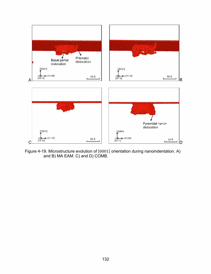
Microstructure Evolution during Nanoindentation for [�����] Orientation
The initial stages of dislocation evolution are shown in Figure 4-15 (MA EAM)
and Figure 4-16 (COMB). When the dislocation starts to form in the area under the
indenter, the deformed structures are similar for both potentials. The prismatic <a>
dislocation and stacking fault on the basal plane are observed as shown in Figure 4-15A
and Figure 4-16A. For the MA EAM potential, a prismatic <a> dislocation form first with
glide plane is parallel to the surface. This is followed by the basal partial <a> dislocation
that connects with one end of the prismatic <a> dislocation. Then another basal partial
<a> dislocation forms and connects with the other end of the prismatic <a> dislocation.
Thus the formation of a dislocation loop that consists of two basal partial <a>
dislocations and one prismatic <a> dislocations is completed. The dislocation loop
glides on the [101�0] surface along the <a> direction. In contrast, for the COMB
potential, as shown in Figure 4-16, the prismatic <a> dislocation continues to glide on
the initial prismatic plane when it forms. At higher stress the pyramidal dislocations form
and glide in addition to prismatic ones; however, no basal dislocations are produced.
This picture is consistent with the energy barrier ratios for the two potentials. In addition,
pyramidal dislocations have only been observed for the COMB potential. Pyramidal
<a+c> dislocation provides the needed deformation in <c> direction.
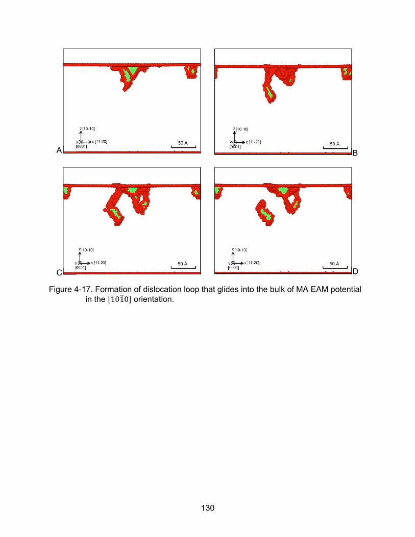
In addition, for the MA EAM potential, dislocation loops form under the indenter
and glide into the bulk, as shown in Figure 4-17. The first defect structure consists of a
leading prismatic dislocation and two basal partials, as shown in Figure 4-17A. This

109
then evolves into a structure that consists of two basal partial dislocations and a
prismatic dislocation gliding into the bulk along the prismatic plane, as shown in Figures
4-17B and 4-17C. The defect structure then starts to break off from the two dislocations.
A similar break-off behavior was also observed in MD simulations of nanoindentation of
a bcc metal 155. The breaking off process of the defect structure is shown in Figure 4-18
from a different direction. We can see that while the two basal partial dislocations and a
prismatic dislocation defect structure glide into the bulk through the screw <a>
component of two dislocations, the two dislocations appear to have edge <a>
components. The two dislocations also move in the <c> direction, as shown in Figure 4-
18B. When the dislocations moving along the <c> direction finally meet, as shown in
Figure 4-18C, the break-off behavior takes place. The final dislocation loop structure is
shown in Figure 4-18D. Thus, while the COMB potential shows dislocation <c>
component through pyramidal <c+a> slip, the MA EAM potential shows a dislocation
<c> component in the dislocation loop formation process.
Microstructure Evolution during Nanoindentation for [����] Orientation
The initial dislocation behaviors of MA EAM and COMB potential for [0001]
orientation are shown in Figure 4-19. For MA EAM, the basal partial dislocation and
prismatic dislocation start to form under the indenter. The basal partial dislocation and
prismatic dislocation forming a dislocation loop glide on the surface (basal plane) along
the <a> direction. For COMB, pyramidal <a+c> dislocations start to form under the
indenter. While because of the higher energy barrier for basal partial dislocations
compared to MA EAM, basal partial dislocations are not expected in the COMB
potential, they are not observed in the MA EAM simulations either. It appears that the
energy barrier for a pyramidal <a+c> dislocation to form is relatively low since we
110
observe pyramidal dislocations in all four orientations for COMB. Also for MA EAM, the
basal partial dislocation and prismatic dislocation seem to facilitate each other, because
basal partial dislocations and prismatic dislocations always connect with each other to
form a loop. Thus the COMB potential displays deformation in the <a> and <c> direction
by pyramidal <a+c> dislocation, whereas the MA EAM potential displays the
deformation in <a> and <c> direction by forming dislocation loops. The detail of the
formation of dislocation loops is shown in Figure 4-20. First, the prismatic <a>
dislocation forms connected with the basal partial dislocations as shown in Figure 4-
20A. Then the basal partial dislocation grows with several jogs that contain a <c>
component as shown in Figures 4-20B and 4-20C; the second prismatic dislocation then
forms. The dislocation loop, consisting of two prismatic dislocations and one basal
partial dislocation, moves along the surface (basal plane) as shown in Figure 4-20D.
The movement of the dislocation loop along the surface is also seen in the [101�0]
orientation. However due to the different orientation, the dislocation loop seen in [101�0]
orientation consists of two basal partial dislocations and one prismatic dislocation.
Summary on Nanoindentation MD Simulation of Zr
In this work, nanoindentation MD simulation has been performed for four different
orientations of single crystal Zr using MA EAM and COMB potentials. The load-
displacement curves present the elastic characteristics in the elastic region for both
potentials. The factors that influence hardness value have been illustrated. Both elastic
and plastic deformations contribute to the hardness value. Due to the small differences
in the reduced modulus for different orientations of the tested four orientations, the
plastic deformation plays a more important role in determining the hardness value. The

111
load drop associated with dislocation behaviors has a direct impact on the hardness
value, with larger load drops tending to lead to a relatively small hardness. Furthermore,
the dislocation behaviors and the atomic structures of the dislocations during the
nanoindentation largely depend on the stable and unstable stacking fault energy and
the ratio of unstable stacking fault energies on different slip planes. The rather small
difference in ������
���������� values leads to very different dislocation behaviors in the
nanoindentation test. For MA EAM, dislocation loops consist of basal partial dislocation
and prismatic <a> dislocation are extensively observed. In contrast, for COMB, no basal
dislocations or dislocation loops are produced. The comparison of the two potential
during nanoindentation shows that the competition between different types of
dislocation on different planes under nanoindentation is mainly determined by the small
difference of the unstable stacking energy on the gliding plane.
In summary, while we see that the specifics of the plastic response depend on
the energetics of the stacking faulty, which differ for the two potentials, the overall
responses for all four surface orientations and for both potentials are rather similar. We
can thus expect that they reasonably well describe the experimental mechanisms of
deformation in Zr.

112
Table 4-1. The reduced modulus for MA EAM and COMB potentials. �[�����]
∗ (GPa) �[�����]∗ (GPa) �[����]
∗ (GPa) ���° �����������∗ (GPa)
MA EAM 114 114 133 129
COMB 125 125 141 121
Experiment 163 109 109 138 106

113
Table 4-2. Total dislocation line length, and number of dislocation segments and junctions calculated using the Crystal Analysis Tool.
Total dislocation line length (Å)
Dislocatio Density (m-2)
Segments Junctions
MA EAM [112�0] 1608 1.17×10¹⁶ 72 36
MA EAM [101�0] 1315 0.96×10¹⁶ 51 23
MA EAM [0001] 1132 0.9×10¹⁶ 67 32
MA EAM 30° orientation 765 4.02×10¹⁵ 32 14
COMB [112�0] 219 3 0
COMB [101�0] 203 7 1
COMB [0001] 0 0 0
COMB 30° orientation 6.1 1 0

114
Figure 4-1. Schematic of the nanoindentation simulation.

115
Figure 4-2. Method used to calculate hardness, after reference 145, 147.

116
Figure 4-3. Relationship between load, hardness and indentation depth for [112�0] orientation. The reported hardness and its uncertainty are obtained for depths bounded by the red dotted lines.

117
Figure 4-4. The loading and unloading curve of Zr using MA EAM potential at 2 ms-1, 5 ms-1, 10 ms-1, 25 ms-1 and 50 ms-1.

118
Figure 4-5. Indentation at 24 Å indentation depth of MA EAM potential using different indentation speed. A) 50 ms-1. B) 5 ms-1. Red atoms represent disordered atoms. Atoms in hcp environments are not shown.
A B

119
Figure 4-6. Load-indentation curves of [101�0] orientation using the MA EAM potential with the thickness of the active region ranging from 90Å to 190Å.
120
Figure 4-7. Deformed structures of [101�0] orientation using the MA EAM potential at 22Å indentation depth. A) 134Å thick active region. B) 168Å thick active region.
A B
121
Figure 4-8. Four different orientations of Zr used in the nanoindentation simulation, with the surface plane shown in blue. A) [0001] orientation. B) [112�0] orientation. C) [101�0] orientation. D) The “30° orientation”. The exposed plane in D is perpendicular to c1.
A B
C D

122
Figure 4-9. Load-displacement curves in the elastic region. A) MA EAM [112�0] and
[101�0] orientation. B) MA EAM [0001] orientation and 30° orientation. C) COMB [112�0] and [101�0] orientation. D) COMB [0001] orientation and 30° orientation. All the data from the MD simulations are fitted using a moving average method.
A B
C D
123
Figure 4-10. Load-displacement curve of four different orientations for the nanoindentation simulation. A) MA EAM potential. B) COMB potential.
A
B

124
Figure 4-11. Hardness of four orientations using MA EAM and COMB potential. The experiment value is from reference 169.
125
Figure 4-12. CNA analysis of Zr indentation at around 26 Å indentation depth using MA EAM. A) [101�0]orientation. B) [112�0] orientation. C) 30° orientation along c-axis. D) [0001] orientation. Red atoms represent the disordered atoms. Green atoms represent the atoms in fcc environment. The atoms in hcp environment are not shown.
A B
C D

126
Figure 4-13. CNA analysis of Zr indentation at around 26Å indentation depth using the COMB potential. A) [101�0] orientation. B) [112�0]orientation. C) 30° orientation along c-axis. D) [0001] orientation.
A B
C D

127
Figure 4-14. Atomic structures of dislocation loop formed during indentation simulation using MA EAM potential. A) [101�0]. B) [112�0].
A B

128
Figure 4-15. Initial stage of dislocation behaviors for MA EAM potential in [101�0] orientation.
A B
C D

129
Figure 4-16. Initial stage of dislocation behaviors for COMB potential in [101�0] orientation.
A B
C D
130
Figure 4-17. Formation of dislocation loop that glides into the bulk of MA EAM potential in the [101�0] orientation.
A B
C D

131
Figure 4-18. Dislocation loop formation process of MA EAM potential in [101�0] orientation.
A B
C D
132
Figure 4-19. Microstructure evolution of [0001] orientation during nanoindentation. A) and B) MA EAM. C) and D) COMB.
A B
C D

133
Figure 4-20. Details of dislocation loop formation in [0001] orientation for MA EAM.
A B
C D

134
CHAPTER 5 NANOINDENTATION OF ZRO2 BY MOLECULAR DYNAMICS SIMULATION
Motivation to study ZrO2
One of the major products of the corrosion process of the zirconium clad inside
the nuclear reactor is zirconia. The corrosion process of the cladding is discussed in the
oxidation of zirconium section of Chapter 2. The properties of the corrosion product
zirconia are discussed in the zirconia system section of Chapter 2. Since the
mechanical integrity of the cladding is essential, it is important to understand its
properties under high stress. In previous chapters we have elucidated the mechanical
response of Zr under tension 150 and under nanoindentation (to understand hardness)
172. It is also important to understand the effects of oxidation on the mechanical integrity
of the clad. Therefore in this chapter, we analyze nanoindentation simulations of
zirconia; in a follow-up chapter we will build on the study of Zr and this chapter to
examine nanoindentation of a zirconia film on a zirconium substrate. In addition to its
presence as a surface layer on clad, zirconia itself is also used as a ceramic biomaterial
173, 174, dental material 175, as a reinforced component in composite materials 176, a fuel
cell electrolyte 177, 178, and as a thermal barrier coating 179; in each of these applications
its mechanical properties are important. In many of the above cases, the cubic zirconia
is stabilized by another element, such as Y. But basic properties still come from the
pure zirconia. So studying the pure zirconia will set the foundations to study all the
above applications.
The empirical potential using COMB 180 formalism introduced in the interatomic
section of Chapter 2 is capable of describing Zr-O-H system 71. The details of ZrO2
COMB potential are discussed in the following section.

135
COMB Potential of ZrO2
In this nanoindentation simulation work, the third-generation charge-optimized
many-body (COMB) potential is used to describe the Zr-O-H system 71, 132; the potential
developed by Noordhoek et al. 71 can describe zirconium, zirconia, zirconium hydride,
and oxygen, hydrogen and water interacting with zirconium. The details of the COMB
formalism and other examples of its applications are described in Chapter 2, and even
more fully elsewhere 104, 180. The development of a potential for such a wide range of
materials inevitably requires some compromises with regards to any specific system.
One of the compromises made in developing this COMB potential is that the ground
state structure of ZrO2 is the cubic fluorite phase.
In addition to the COMB potential, there are many other potentials for ZrO2 in the
literature 181-187. Six interatomic potentials based on Buckingham potential form for
yittria-stablized zirconia (YSZ) were assessed by Yin et al. 188. For example, the
Schelling potential, using Buckingham type short-ranged potential and a Coulomb
electrostatics term, can describe both the cubic and tetragonal phases; this potential
was also able to describe yttria-stablized zirconia (YSZ) 181. However the Buckingham
potential is a fixed charge potential and thus cannot describe zirconium or oxygen
separately. The ReaxFF formalism, a variable charge reactive potential, has been
parameterized for YSZ to study the oxygen ion transport 183. The relative energies of a
few phases agrees well with the quantum mechanics results. However the ReaxFF
potential does not currently include the monoclinic phase and ZrHx system. And the
ability to describe the deformation behaviors is unknown.
In summary, the COMB potential is capable of describing many of the key
properties of the Zr-O-H system 71, 132, albeit with less than ideal materials fidelity. The

136
current parameterization of the COMB potential can only describe the cubic fluorite
phase; while this is a clear limitation, the observed presence of the cubic fluorite on the
Zr surface by electron diffraction 68-71 indicates that it can provide valuable information
of such systems. Therefore, COMB will be used to study the mechanical properties of
ZrO2.
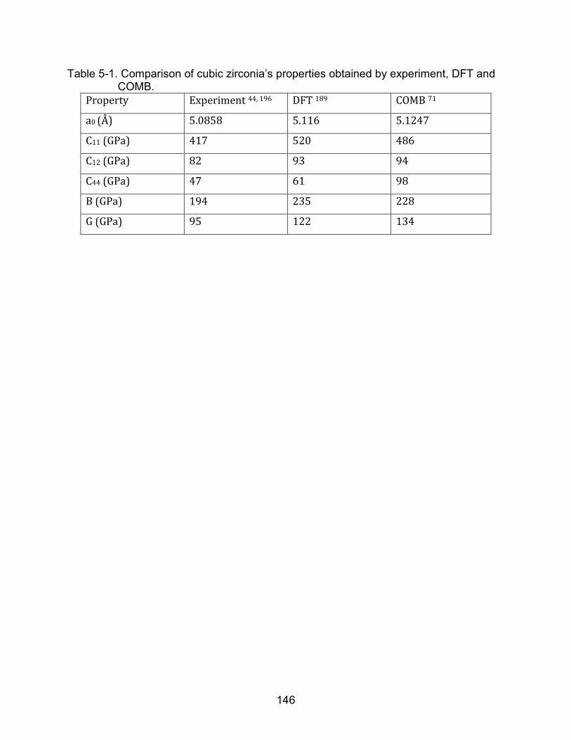
Here we only summarize the key properties of the potential with regards to
representation of the c-ZrO2; other properties are described elsewhere 71. The elastic
constants except for C44, bulk modulus and shear modulus match well with DFT 189
results as shown in Table 5-1 71. Of the point defect formation energies listed in Table 5-
2, the O vacancy, Zr vacancy and Zr interstitial formation energies predicted by COMB
potential are higher than the DFT calculations, while that of the O interstitial is
underestimated significantly comparing to DFT 71. Due to the presence of the high
stress concentration in nanoindentation simulation, the above discrepancy of the defect
formation energy will not significantly influence the deformation outcomes. As in the Zr
nanoindentation study of chapter 4 172, the reduced modulus along [110] and [100] have
been calculated, 370 GPa for [110] orientation and 468 GPa for [100] orientation. The
reason for choosing the [110] and [100] orientations is given in the orientation section
below.
Simulation Setup
Nanoindentation MD simulations of cubic zirconia were performed using
LAMMPS 158. The simulation set up is the same as that of the Zr nanoindentation
simulations discussed in Chapter 4. The simulated system consists of 3 regions; from
top to bottom: an active region, a thermostat region and a fixed region. The force
exerted by the spherical indenter is applied to the active region, which is achieved by

137
using the “fix indent” fix style in LAMMPS. The description of the applied force can be
found in Equations 4-1 and 4-2. The details of the simulated system are shown in Figure
5-1.
Orientation
Both the [110] and [100] orientations of cubic zirconia have been observed in
oxidized Zr by electron diffraction 68-71; thus, these are chosen for our simulation study.
The comparison of the [110] and [100] orientations will probe the anisotropy of ZrO2. In
addition, our simulation results can then be compared with those of the indentation
experiments on [110] and [100] orientations of YSZ 190. The (110) plane is the charge
neutral plane as shown in Figure 5-2A. The structure in the [100] direction consists of
alternating planes of Zr and O and thus has a dipole moment normal to the surface.
Charged planes can be expected to reconstruct 191, 192. For example, for (001) of rock-
salt structure, the octopolar reconstruction can considerably lower the energy and
reduce the surface stress 191. In order to minimize the charged surface effect the top
and bottom surface (100) plane are reconstructed by hand. First the top and bottom
surfaces are set to be Zr planes. As a result, there is an extra Zr plane in the system.
Then the atoms in the face center position of the top and bottom Zr planes are removed.
Thus, after this modification, the (100) surface has a pyramid shape with (110) charge
neutral plane facets and the ZrO2 stoichiometry is conserved, as shown in Figure 5-2A.
Before nanoindentation, the two surface systems are fully relaxed under NPT
condition. For the charge neutral (110) plane, the surface structure after relaxation is
shown in Figure 5-2B. The surface oxygen layer splits into two oxygen layers. The Zr
atoms stay at their lattice sites after relaxation. The charge of the surface Zr atoms is
less positive than that of the Zr atoms in the bulk; and the charge of oxygen atoms at

138
the surface becomes less negative. For the reconstructed (100) charged plane, the Zr
and oxygen atoms at the surface leave their original position to form a relatively low
energy configuration. The charge of Zr atoms at the surface becomes less positive
compared to those in the bulk. And the charge of O atoms at the surface becomes less
negative compared to those in the bulk.
Effect of Indentation Speed and Temperature
The possible effects of indentation speed and temperature are addressed first.
Because it involves charge equilibration, the COMB potential is more computationally
demanding than standard fixed-charge empirical potentials. Choosing the appropriate
indentation speed that can both give physically reasonable results and minimize the
computational time is thus important. Nanoindentation MD simulations on CaCO3
minerals using 10ms-1 and 30ms-1 generates almost the same load-displacement curve
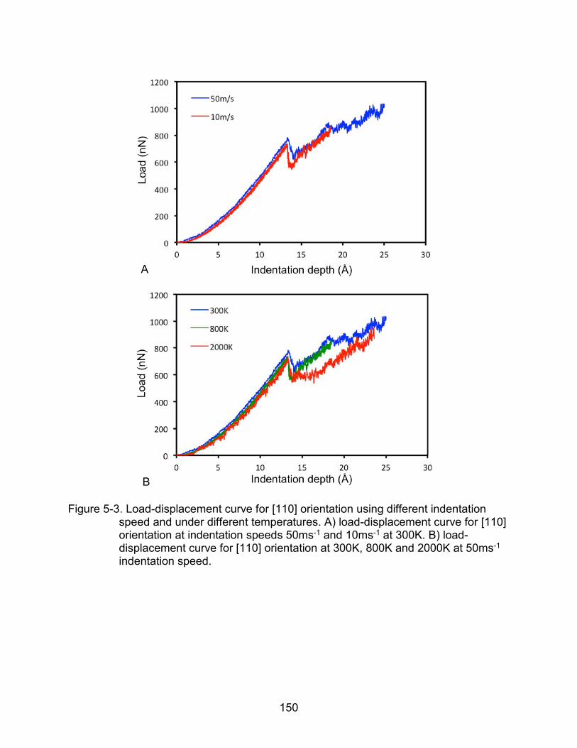
193. Indentation simulations at 10ms-1 and 50ms-1 are tested here; as shown in Figure 5-
3 for the [110] orientation, the load-displacement curves almost overlap at 300K. Most
importantly, the load drops related to the plastic deformation both happen at
approximately the same displacement of 13 Å.
Examining the effect of temperature using an indentation speed of 50ms-1, the
load-displacement curves almost overlap with each other for 300K, 800K and 2000K
especially before the first load drop. There is a small amount of elastic softening as the
temperature increases; however, the load drops related to the plastic deformation takes
place at an indentation of 13 Å for all temperatures.
The results indicate that the effects of temperature and indentation speed on the
indentation simulation results are not that significant. In subsequent simulations, we

139
thus use an indentation speed of 50ms-1 to minimize computing time and a temperature
of 300K to minimize thermal fluctuations.
Using Hertz Law to Rescale MD Simulation Data
Hertz continuum elastic contact analysis has been widely used to describe the
elastic deformation behavior for spherical indenter. Here, the Hertz Law will be used to
rescale the MD data to the time and length scale of nanoindentation experiment. Within
Hertz theory, the load applied by the indenter, P, is given by 161, 162,
� =�
��∗�
�
�ℎ�
� (5-1)
where R is the radius of curvature of the indenter, h is the indentation depth, and �∗ is
the reduced modulus, defined as 161, 162,
�∗ = �����
�
��+
�����
���
��
(5-2)
where �� and �� are Young’s modulus and Poisson’s ratio of the sample and �� and ��
are Young’s modulus and Poisson’s ratio of the indenter. For the hard indenter E=∾ and
=0.
According to Equation 5-2, the reduced modulus �∗ is the only materials related
property. So we consider �∗ as a constant, independent of the indenter size and
indentation depth. The relationship between loads from different nanoindentation tests
using different indenter sizes (R1 and R2) and indentation depth under the same
indentation speed can be expressed as
��
��= �
��
���
��
���
�
� (5-3)
where P1 and P2 are the load responses, and h1 and h2 are the indentation
depths at different scales. In our study, P1 is at the nN scale, while R1 and h1 are at Å

140
scale. For the experiments we compare with, P2 is at μN scale, and R2 and h2 are
hundreds of nms. Hertz law is first used to examine whether the simulation results show
elastic behavior in the elastic regime. According to Hertz law the load P should have
linear relationship with h3/2. Furthermore, the simulation results are rescaled to compare
with the experiments 190 according to Equation 5-3.
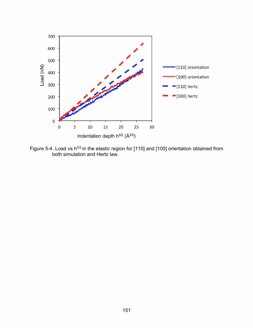
Elastic Deformation
At the beginning of the indentation test, the system deforms elastically. In the
elastic region, the load vs h3/2 curves are compared for the data from the simulation and
the data calculated according to Hertz Law. As shown in Figure 5-4, the load vs h3/2
curves obtained from the simulation are linear, which represents the elastic behavior.
The reduced modulus calculated using the potential predicted elastic constant of [110]
and [100] orientations are 370 GPa and 468 GPa. According to Equation 5-1, the slope
of the load-displacement in the elastic region of the [100] orientation should be steeper
than that of the [110] orientation. In the simulations, the slope of the [100] orientation is
initially slightly steeper than that of the [110] orientation, which is consistent with the
order predicted by the Hertz law. However the [100] orientation shows a softening with
increasing load. The above difference can be caused by the system size effect
observed in the Zr nanoindentation simulation discussed in chapter 4 172.
Having established that the elastic part of the indentation displays Hertz Law, we
can rescale the length scale of MD to compare with experimental results, obtained for
much larger indenters (350nm) and indentation depth at nanometer scale. The rescaling
is based on Equation 5-3. The rescaled results are compared to the nanoindentation
experiments on yttria-stabilized zirconia with 10%mole of yttria 190. According to an
experimental study of yttria-stabilized zirconia with mole% of yttria ranging from 11% to
141
18%, the Young’s and shear moduli decrease as the mole% of yttria increases, while
the anisotropy factor increases as the mole% of yttria increases 194.
As shown in Figure 5-5, the rescaled load-displacement curves from the MD
simulations match quite well with those from the indentation experiments on single
crystal YSZ. The simulation results match better with the experiments for [110]
orientation. For [100] orientation, the simulation results agree well with the experiment
for low loads prior to the softening discussed above.
The YSZ indentation experiments show that the slope of load-displacement of
[100] orientation is steeper than that of [110] orientation, which is consistent with MD
results and Hertz Law prediction. The difference between the load-displacement of [110]
and [100] orientations in our simulation is smaller than that in the experiments, which
can be caused by the increased anisotropy factor due to the yttria doping 194.
Plastic Deformation
The first load drop typically represents the initiation of the plastic deformation. As
shown in Figure 5-6, the first load drop for the [110] orientation takes place at ~13 Å
indentation depth, while for [100] orientation, the first load drop is at ~10 Å. After
rescaling, the first load drop should be at ~10nm for [100] orientation and ~13nm for
[110] orientation. The earlier yield for [100] orientation simulation agrees reasonably
well with the indentation experiments on YSZ, which the first load drop for [100] and
[110] orientations at 14nm and 22 nm respectively 190. The simulated yield strength of
the [110] orientation (~800nN) is twice as much as that of the [100] orientation
(~400nN). This is also in consistent with the experimental results 190 which the yield
strength of the [110] and [100] orientations are ~500μN and ~250μN respectively.

142
The deformed atomic structures at an indentation depth of 25Å are shown in
Figure 5-7. The atomic pileups represented by the uncoordinated atoms in Figure 5-7
are seen in both [110] and [001] orientations. It is obvious that the shapes of the
deformed regions are very different for the two orientations. The origin of this difference
resides in the anisotropy and the limited slip systems of ZrO2. For the [110] orientation,
as we can see from the side view (001) plane, Figure 5-7A, and from the side view
(110) plane, Figure 5-7C, that the boundary between the deformed and the un-
deformed regions lie along the <110> direction. The boundary between the deformed
region and un-deformed region in the [100] orientation is also along the <110> direction
as shown in Figure 5-7B. This preference for deformation along the <110> direction
during nanoindentation is consistent with <110> being the dominant slip direction for the
ZrO2 system. As introduced in the simulation analysis tool section in chapter 2, the
Dislocation Extraction Algorithm (DXA) can be used to capture dislocation structures.
First, the DXA is applied to the deformed structure with O atoms being removed so that
the Zr can be treated as an fcc sublattice. No dislocation structures are captured by the
DXA. By contrast indentation simulations of fluorite-structured CaF2 did show the
generation of dislocations as the first plastic event took place 195.
As the DXA is unable to capture any dislocations in the deformed structure, more
detailed analysis of evolution of the atomic structure is necessary in order to understand
how the structure transforms around the first load drop at the atomic level. First, the
volume change during indentation at different places in the pile up region of [110]
orientation is analyzed. A few tetrahedra defined in Figure 5-8 are chosen from different
deformed regions to study the volume change. In the pile up region, the volume of the
143
system decreases significantly at the load drops in the load-displacement curve. As
shown in Figure 5-8, the volume of the tetrahedron in the blue circle region shows no
significant change through the indentation process. The volume of the tetrahedron in the
purple region starts to decrease significantly at an indentation depth of ~14 Å, which
corresponds to the first load drop in the load-displacement curve. Furthermore, starting
at ~18 Å indentation depth, the volume of the tetrahedron in the red circle region shows
significant decreases, which correspond to the second load drop in the load-
displacement curve. The volume of the tetrahedron in the green circle region starts to
decrease at ~16 Å. That is, the region close to the indenter deforms first, then the
further region deforms subsequently. Although no dislocation lines are captured in the
deformed structure, the significant volume decreases proves that the load drop is
caused by some structural changes.
Next, we analyze the evolution of the atomic structure of [110] orientation at the
load drop. We first examine representative (100) and (110) planes in the [110]
orientation to see how the system deforms. We pick out one (110) plane and one (100)
plane inside the regions that deform during the nanoindentation. For the (100) planes
shown in Figures 5-9(a) and (b), the atomic position in the deformed area only change
slightly along [100] direction although there is force applied along [100] direction by the
indenter. For the (110) plane shown in Figures 5-9(c) and (d), the atomic plane deforms
significantly along the [110] direction. For the spherical indenter used here, the forces
applied along [110] (x-axis) and [100] (y-axis) are equal. By the comparison shown in
Figure 5-9, we can conclude that the structure prefers to deform along [110] direction
with [100] direction being the hard direction.

144
The Zr atoms on ZrO2 lie on an fcc lattice and thus have 12 Zr neighbors. Close
to indenter, there are a number of 13-coordinated Zr atoms, shown as red atoms in
Figure 5-7. The structural change in the above 13-coordinated atoms region is shown
in Figure 5-10. The xz-(100) plane deforms along [100] to transform to a closed packed
plane with 13 coordination numbers during indentation. The distance between nearest
neighbor is ~2.8 Å. The structure of xy-(100) plane stays unchanged during the
indentation. So the highly deformed region can be regarded as a closed pack structure
with AAA stacking sequence along y-<100> direction. The transformation of the O
lattice is similar to the Zr as shown in Figure 5-11. On the xz-(100) plane, the O atoms
squeeze along [110] direction. The O atoms also form a higher density structure.
The charge distribution of [110] and [100] orientation after nanoindentation
simulation is shown in Figure 5-12. The pile up region and the boundaries between the
deformed and un-deformed region can also be represented by the charge distribution.
As we can see the charge of Zr atom becomes less negative in the deformed region;
the charge of the O atoms become less negative.
Hardness
The hardness for the two orientations is calculated using the same method
discussed in the hardness calculation method section of Chapter 4 172. Briefly, as shown
in Figure 5-13, the hardness keeps increasing with indentation depth until the first load
drop. After the first load drop, the hardness value stays relatively constant. We take as a
representative hardness the average between the two dashed lines. The quoted error
represents the standard deviation within the two red dotted lines region. The
nanoindentation simulation yields a hardness value of 19.8±0.6 GPa for [110]
orientation and 14.6±0.3 GPa for [100] orientation.

145
Our previous nanoindentation MD study on single crystal Zr with different
orientations using COMB potential gave calculated hardness over the range from 3.5
GPa to 6 GPa. The comparison of load-displacement curve of [0001] Zr and [110] ZrO2
is shown in Figure 5-14. The load response of ZrO2 is much higher than that of Zr as we
expected. Moreover, the plastic deformation happens much earlier for Zr than for ZrO2
consistent with the stronger propensity of hcp metals to deformation than ionic
materials.
Summary on ZrO2
This work addresses the deformation process of cubic ZrO2 in both [110] and
[100] orientations. In the elastic deformation regime, the MD simulation results agree
with the Hertz Law. After rescaling, the MD data is very comparable to the experiments.
Furthermore, the anisotropy predicted by MD simulation is confirmed by the experiment
and the classical theory. Yield behaviors are seen in both [110] and [100] orientations.
The earlier yielding for [100] orientation is consistent with the experiment. All the above
agreement with experiment proves the fidelity of this ZrO2 potential. In the plastic
deformation regime, the structural transformation at atomic level is analyzed. The
reason for the absence of dislocation line structure is not clear. The analysis of the
structural transformation indicates that the structure tends to deform along [110]
direction. As the COMB potential is a variable charge potential, the charge evolution is
also analyzed. When Zr and O atoms are at surface area or in the deformed region,
both of their charge tends to decrease. This study on ZrO2 builds the foundation to
study the ZrO2/Zr system.
146
Table 5-1. Comparison of cubic zirconia’s properties obtained by experiment, DFT and COMB.
Property Experiment 44, 196 DFT 189 COMB 71
a0 (Å) 5.0858 5.116 5.1247
C11 (GPa) 417 520 486
C12 (GPa) 82 93 94
C44 (GPa) 47 61 98
B (GPa) 194 235 228
G (GPa) 95 122 134

147
Table 5-2. Point defect formation energies predicted by DFT and COMB in cubic zirconia.
Point defect DFT (cubic phase) 71, 197 COMB (cubic phase) 71
O vacancy (eV) 6.15 11.2
O interstitial (eV) 3.46 0.37
Zr vacancy (eV) 15.00 27.9
Zr interstitial (eV) 1.78 4.17

148
Figure 5-1. Details of the simulated [110] oriented ZrO2 system.
149
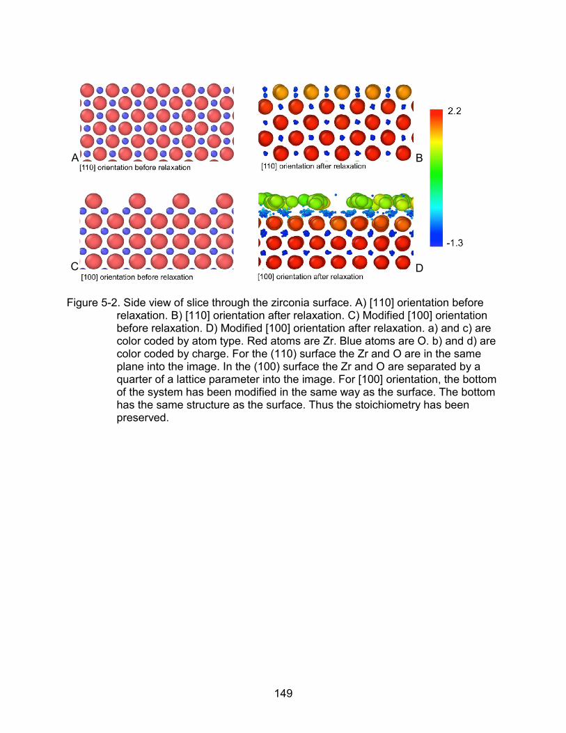
Figure 5-2. Side view of slice through the zirconia surface. A) [110] orientation before relaxation. B) [110] orientation after relaxation. C) Modified [100] orientation before relaxation. D) Modified [100] orientation after relaxation. a) and c) are color coded by atom type. Red atoms are Zr. Blue atoms are O. b) and d) are color coded by charge. For the (110) surface the Zr and O are in the same plane into the image. In the (100) surface the Zr and O are separated by a quarter of a lattice parameter into the image. For [100] orientation, the bottom of the system has been modified in the same way as the surface. The bottom has the same structure as the surface. Thus the stoichiometry has been preserved.
A B
C D
150
Figure 5-3. Load-displacement curve for [110] orientation using different indentation
speed and under different temperatures. A) load-displacement curve for [110] orientation at indentation speeds 50ms-1 and 10ms-1 at 300K. B) load-displacement curve for [110] orientation at 300K, 800K and 2000K at 50ms-1 indentation speed.
A
B
151
Figure 5-4. Load vs h3/2 in the elastic region for [110] and [100] orientation obtained from
both simulation and Hertz law.

152
Figure 5-5. Load-displacement curve comparison between rescaled MD data and
experimental data. The experimental data shown as YSZ [100] Exp. and YSZ [110] Exp. is obtained from reference 190. [110] Sim. and [100] Sim. are the simulation results.

153
Figure 5-6. Load-displacement curves for [110] and [100] orientation under indentation
at 300K for speed of 50ms-1.

154
Figure 5-7. Side view of deformed structure of ZrO2 at indentation depth of 25Å. A) [110]
orientation side view (001) plane. B) [001] orientation side view (001) plane. C) [110] orientation. The color scheme represents the coordination number. Only Zr atoms are shown in the figure.
A B
C

155
Figure 5-8. Volume change of a tetrahedron in the deformed area during nanoindentation simulation for [110] orientation. Atom 1, 2, 4 and 4 form the tetrahedron.

156
Figure 5-9. Analysis of indentation in [110] orientation. A) One (100) plane before nanoindentation simulation. B) The same (100) plane after nanoindentation simulation. C) One (110) plane before nanoindentation simulation. D) One (110) plane after nanoindentation simulation. Both planes lie under the indenter.
A B
C D

157
Figure 5-10. The transformation of highly deformed region with 13 coordination number
in [100] orientation during indentation. Yellow atoms represent 12 coordination numbers. Red atoms represent 13 coordination numbers.

158
Figure 5-11. The transformation of highly deformed region with both Zr and O atoms in
[100] orientation. The atoms are color coded by atom type. Red atoms are Zr and blue atoms are O atoms.

159
Figure 5-12. Charge profile in side view of deformed structure of ZrO2 at indentation depth of 25Å. A) [110] orientation side view (001) plane. B) [001] orientation side view (001) plane. The atoms are color coded by charge.
A B

160
Figure 5-13. Hardness vs indentation depth for [110] orientation.

161
Figure 5-14. Load-displacement curve of [0001] Zr and [110] ZrO2.

162
CHAPTER 6 NANOINDENTATION OF ZRO2/ZR BY MOLECULAR DYNAMICS SIMULATION
Chapter 3 addressed the deformation behaviors of polycrystalline Zr.
Nanoindentation simulations were performed on four orientations of single crystalline Zr
and two orientations of single crystalline cubic ZrO2 in Chapters 4 and 5 respectively.
This understanding of the deformation behaviors of Zr and ZrO2 constitutes a solid
foundation to move on to the study of ZrO2/Zr system; that is a thin ZrO2 layer on top of
a Zr substrate. In this chapter, the Zr and ZrO2 interface is first studied by using COMB
potential. Then the nanoindentation simulations of ZrO2/Zr system are performed to
study to deformation behaviors. Finally, the results from Zr, ZrO2 and ZrO2/Zr systems
are compared.
Zirconia/zirconium Interface
As discussed in the oxidation of zirconium section of Chapter 2, a zirconium
oxide layer forms during clad corrosion. The COMB potential can describe the Zr-O-H
system. As discussed in Chapter 5, the ground state of ZrO2 predicted by the COMB
potential is cubic. The simulated metal/oxide system consists of [0001] orientation Zr
and [110] orientation ZrO2 as shown in Figure 6-1. Oxidation on Zr (0001) surface has
been studied extensively 68, 198-203. As discussed in the Orientation section of Chapter 5,
the [110] orientation of ZrO2 has been observed in oxidized Zr by electron diffraction 68-
71; (110) plane is a charge neutral plane that does not has a dipole moment normal to
the surface plane. Discussed in the texture in zirconium section of Chapter 2, [0001]
orientation is the main texture observed in Zircaloy 39. So the Zr-[0001] orientation with
ZrO2-[100] orientation on top is chosen as the simulation system. A schematic of the
simulated system is shown in Figure 6-1. In order to reduce the lattice mismatch

163
between Zr and ZrO2, the number of unit cells of Zr and ZrO2 along x and y directions
has been chosen such that total strain is less than 1% along x direction and less than
3% along y direction. The work of separation of Cu/ZrO2 system calculated using DFT is
1.96 Jm-2 for one of the configurations of Cu-(001)/ZrO2-(110) interface 204. The work of
adhesion of our simulated system is 2.31 Jm-2, which is comparable to the above DFT
results. The atomic structure of the system before and after relaxation is shown in
Figure 6-2. The O atoms diffuse to the second layer of Zr substrate as shown in Figure
6-2B. The charge of the O atoms in the interface area becomes less negative. As
shown in Figure 6-2C, the structure of three layers of Zr atoms in Zr substrate and two
layers of Zr atoms in ZrO2 at the interface changes. The charge of Zr in ZrO2 becomes
less positive at the interface while with the charge of Zr atoms in Zr substrate in the
interface region becomes more positive. The oxygen density is shown in Figure 6-3 and
the shear strain map at the interface is shown in Figure 6-4. The O atoms start to move
around their perfect lattice sites during relaxation, which corresponds to the broadening
of the O density peak in Figure 6-3. The first two peaks in Figure 6-3 at the ZrO2 surface
correspond to the splitting of the first O layer at the ZrO2 surface, which is also seen at
the surface of pure ZrO2 after relaxation. The O density peaks start to decrease and
broaden close to the interface. The O atoms diffuse across the interface to the second
layer of the Zr metal substrate. After relaxation, a strain field exists at the interface, as
shown in Figure 6-4. Two layers of ZrO2 and three layers of Zr at the interface have
been strained. The structures of the first layer of Zr, Figure 6-4B, and the first layer of
ZrO2, Figure 6-4C, are distorted, but do not transform to different structures. At the
interface, the Zr substrate experiences higher shear strain than the ZrO2 layer. The
164
charge of Zr decreases from ZrO2 to Zr across interface along with the charge of O
decreases from ZrO2 to Zr across interface as shown in Figure 6-5A. The above charge
transfer at the interface result in the formation of a dipole moment at the interface seen
in Figure 6-5B between 25 Å and 30 Å. In addition, the charge of Zr and O atoms
decreases at the ZrO2 surface seen in Figure 6-5A before 5 Å. A dipole moment forms
within the ZrO2 surface layer shown in Figure 6-5B before 2 Å. The total charge inside
the ZrO2 layer and Zr substrate is zero.
Simulation Setup
The nanoindentation simulation set up for ZrO2/Zr system is the same as the set
up for Zr and ZrO2 systems introduced in Chapter 4 and Chapter 5. The simulation is
performed at 300K with a 10ms-1 indentation speed. Common Neighbor Analysis 126, 127
and the Dislocation Extraction Algorithm (DXA) 123, 125 are used to analyze the deformed
structures.
Load-displacement Curve and Hardness
The load-displacement curve and the hardness versus indentation depth are
shown in Figure 6-6. In the load-displacement curve, no significant yielding is seen until
18 Å indentation depth where the load starts to decrease. The hardness first increases
with the indentation depth. Then it becomes stable and fluctuates between 13 Å and 18
Å. After yielding at around 18 Å, the hardness starts to decrease. Unlike the case in Zr
and ZrO2 nanoindentation simulation seen in Figure 4-3 and Figure 5-13, the hardness
first increases with the indentation depth and after certain indentation depth it becomes
stable. As discussed in Chapter 4, hardness largely depends on the deformation
behaviors. The above difference for ZrO2/Zr might be explained by the later deformation
analysis.

165
The comparison of load-displacement curve for Zr-(0001), ZrO2-(110) and ZrO2-
(110)/Zr-(0001) is shown in Figure 6-7. It can be concluded from Figure 6-7 that the
ZrO2 is the hardest and Zr is softest, while the ZrO2/Zr system resides in the middle. As
a metal system, it is reasonable that the Zr system yields at the most shallow
indentation depth, around 5 Å. However, the hardest ZrO2 yields at around 13 Å, while
the softer ZrO2/Zr system yields at 18 Å. Based on the fact that the yield happens at 5 Å
for pure Zr, the Zr substrate in ZrO2/Zr system is expected to yield before 18 Å. It raises
the questions as to at what depth the Zr substrate in ZrO2/Zr system starts to yield and
what activity causes the load drop at 18 Å indentation depth. The above questions are
expected to be answered by the deformation analysis later.
Deformation Process during Nanoindentation Simulation
The deformed structure during nanoindentation simulation is shown in Figure 6-8.
In Figure 6-8, the O atoms have been removed from the visualization. The Zr atoms are
in an fcc environment in the ZrO2 layer and in an hcp environment in the Zr substrate.
So, CNA can be applied separately in Zr and ZrO2 to identify fcc-like atoms, hcp-like
atoms and disordered atoms. DXA can be used to extract dislocation lines. As
discussed in Chapter 4, the DXA is not very successful of capturing the dislocations line
in pure Zr COMB simulations. Thus, DXA will mainly be used here to capture the
dislocation lines in ZrO2. Dislocations start to nucleate in the Zr substrate at around 12
Å as shown in Figure 6-8A. The 12 Å indentation depth correspond to the b point in the
load-displacement curve seen in Figure 6-6. It answers the question raised in the
previous section that the Zr substrate starts to deform plastically at 12 Å before the yield
point c seen in Figure 6-6 at 18 Å. However unlike pure the Zr system seen in Figure 6-
7, no significant load drop is observed in the load-displacement curve for ZrO2/Zr

166
system when plastic deformation happens in Zr substrate. So, with the presence of the
ZrO2 layer, the plastic deformation of Zr substrate is delayed compared to the pure Zr
system and can hardly be identified in the load-displacement curve. The dislocation
lines in the top ZrO2 layer are captured by DXA at an indentation depth of 18.5 Å as
shown in Figure 6-8B. The green dislocation line in Figure 6-8B is a 1/6<110> Shockley
partial, while the Burgers vector of the red dislocation cannot be identified by the DXA.
The deformed structure corresponds to point c in Figure 6-6. This answers the other
question raised in the previous section: the load drop at around 18 Å is caused by the
plastic deformation in the top ZrO2 layer. Before the formation of dislocation in ZrO2 at
around 18 Å, the ZrO2 layer deforms the along [110] direction in the same way as
discussed in Chapter 5 (see Figure 5-7). In addition, dislocation lines have been
identified by DXA in ZrO2 layer of ZrO2/Zr system rather than in the pure ZrO2 system.
However, the ZrO2 layer in ZrO2/Zr system turns out to generate dislocations during
nanoindentation simulation, which might be caused by the presence the heterogeneous
interface and the fact that the ZrO2 layer in ZrO2/Zr system is a thin film.
The hardness of the ZrO2/Zr system increases as the indentation depth increases
until 13 Å, where the plastic deformation begins. Then it becomes stable and fluctuates
between 13 Å and 18 Å. The above characteristic is the same as the pure Zr case seen
in Figure 4-3. The hardness starts to decrease after 18 Å where the load starts to drop
and the dislocations start to form in ZrO2 layer. For pure ZrO2 system, the hardness
decreases after load drop and becomes stable later, as seen in Figure 5-13. So we
speculate that if we indent deeper than 24 Å, the hardness might become stable.
However, when we do actually indent deeper than 24 Å, the ZrO2/Zr system fails and

167
the ZrO2 fragments in an explosive manner as it is not able to absorb more energy. The
failed system is shown in Figure 6-9. In summary, before plastic deformation takes
place in ZrO2 layer, the characteristic of the relationship between hardness and
indentation depth agrees with the pure Zr system. After plastic deformation takes place
in ZrO2 layer, characteristic of the relationship between hardness and indentation depth
is similar to the pure ZrO2 system.
The evolution of the volumetric strain is shown in Figure 6-10. The method to
calculate atomic-level strain tensors can be found in References 205, 206. The reference
configuration of the system to calculate the atomic strain tensors is set to be the relaxed
ZrO2/Zr system before indentation. The first highly strained region locates at the
interface right under the indenter as shown in Figure 6-10A. The stress firstly passes to
the Zr substrate at the interface. In the above strained region, a dislocation starts to
nucleate in the Zr substrate, which correspond to point a in the load-displacement curve
shown in Figure 6-6. In Figure 6-10B, as the highly strained region continues to grow in
the Zr substrate, the Zr surface that contacts with the indenter becomes highly strained.
Then the highly strained region starts to appear inside the ZrO2 layer as shown in
Figure 6-10C. This region works as the dislocation nucleation site in the ZrO2, which
correspond to the point b in the load-displacement curve shown in Figure 6-6 where
dislocation lines starts to be observed in ZrO2. The strain does not accumulate at the
interface except for the area right under the indenter.
Summary on ZrO2/Zr
This work focuses on the deformation behaviors of ZrO2/Zr system during
nanoindentation simulation. The deformation behaviors are compared with those from
pure Zr and pure ZrO2 systems. The difference and similarities are illustrated.

168
In the load-displacement curve, the starting point of the plastic deformation in the
Zr substrate can hardly be identified; the starting point of the plastic deformation in ZrO2
layers is identified by the load decreases. The plastic deformation in both ZrO2 layer
and Zr substrate are delayed in ZrO2/Zr system comparing to pure ZrO2 and Zr case.
The relationship between hardness and indentation depth has two stages. The
first can be represented by the pure Zr system. The second stage can be represented
by the pure ZrO2 system. The two stages are distinguished by the point where plastic
deformation starts to take place in ZrO2 layer.
The specific deformation processes in Zr substrate and ZrO2 layer are the same
as those in pure Zr and pure ZrO2 except that dislocation lines are captured by DXA in
ZrO2 layers of ZrO2/Zr system.

169
Figure 6-1. Schematic of the simulated ZrO2/Zr system.

170
Figure 6-2. ZrO2 and Zr interface. A) ZrO2/Zr system before relaxation. Red atoms
represent Zr and blue atoms represent O. B) Charge map of O atoms after relaxation. Only O atoms are shown. C) Charge map of Zr atoms after relaxation. Only Zr atoms are shown.
A B C

171
Figure 6-3. O density profile in ZrO2/Zr system. Position at 0 Å represents the ZrO2
surface.

172
Figure 6-4. Shear strain map at the interface of ZrO2/Zr system after relaxation. Color scheme represents the shear strain. O atoms have been removed. A) Side view of ZrO2/Zr system. B) Top view of the first layer in Zr at the interface. C) Top view of the first layer in ZrO2 at the interface.
A
B
C

173
Figure 6-5. Charge profile across across the ZrO2/Zr interface. A) Average charge of Zr
and O across the ZrO2/Zr interface. B) Total charge density across the ZrO2/Zr interface.
A B
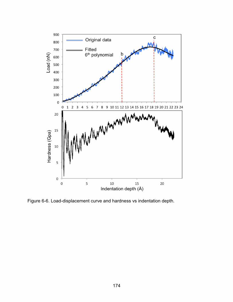
174
Figure 6-6. Load-displacement curve and hardness vs indentation depth.
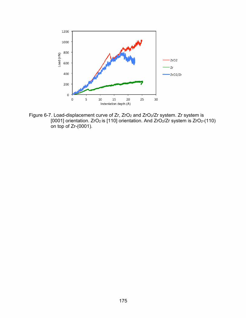
175
Figure 6-7. Load-displacement curve of Zr, ZrO2 and ZrO2/Zr system. Zr system is
[0001] orientation. ZrO2 is [110] orientation. And ZrO2/Zr system is ZrO2-(110) on top of Zr-(0001).

176
Figure 6-8. Deformed structure of ZrO2/Zr system after nanoindentation. A) Deformed
structure at 12.4 Å indentation depth. The red atoms represent disordered atoms. Atoms in fcc and hcp environment have been removed. B) Deformed structure at 19 Å indentation depth. The atoms in ZrO2 layer have been removed. Only dislocation lines are shown. Green lines represent the Shockley partials. Red lines represent other dislocations types. The dislocation lines are captured using DXA.
A B

177
Figure 6-9. The failure of the ZrO2 layer. Red atoms represent Zr atoms. Blue atoms represent O atoms.

178
Figure 6-10. Evolution of volumetric strain during nanoindentation simulation. Atoms
with volumetric strain value smaller than 0.02 are removed. A) Volumetric strain map at indentation depth of 12 Å. B) Volumetric strain map at indentation depth of 15.3 Å. C) Volumetric strain map at indentation depth of 18.6 Å. D) Volumetric strain map at indentation depth of 21.2 Å. The color scheme is volumetric strain.
A B
C D

179
CHAPTER 7 CONCLUSIONS
This work has studied the mechanical properties of Zr, ZrO2 and ZrO2/Zr systems
using molecular dynamics as the simulation tool. Understanding the basic deformation
behaviors of Zr-O system can help to design better zirconium-based cladding.
Furthermore, our results are not only limited to the specific Zr and its oxide system but
also a representative of at least some other hcp metal systems, fluorite ionic systems
and metal-oxide heterogeneous systems. In addition, the nanoindentation simulation
performed on the ZrO2/Zr system is the first mechanical MD simulation done on
ionic/metallic heterogeneous system.
The expected deformation modes including various dislocations have been
observed in the 2D textured and 3D polycrystalline structures for both EAM and COMB
potential. The two potentials’ ability to describe mechanical properties is thus
demonstrated.
For 2D textured structure, the activated deformation mode is determined by the
texture. Despite differences in detail predicted by the two used potentials, the yield
deformation behaviors are very similar. For the 3D structure, the experimentally
observed primary slip system is prevalent, while the experimentally observed secondary
slip systems are rare or absent. In the nanoindentation simulation, the dislocation
processes are manifested in different ways. In particular, the various slip systems have
more freedom to compete with each other. Moreover, the dislocation behaviors are well
related to the unstable stacking fault energy. As a result, the yield deformation
behaviors have a lot of difference for the two potentials, reflecting the differences in
these energy barriers.

180
The stable and unstable stacking fault energy play an important in determining
the deformation behaviors. The ratio of the stacking fault and unstable stacking fault
energies along the dislocation gliding direction can determine whether the dislocation is
a full dislocation or a partial dislocation. If the above ratio is close to unity, the
dislocation will be a full dislocation; if the ratio is close to zero, the dislocation will be a
partial dislocation. The partial dislocation can also form under scenario that the energy
barrier along an indirect gliding path is smaller than that along the direct gliding path.
The unstable stacking fault (energy barrier) on different gliding planes determines the
primary slip system. The competition among different slip systems is controlled by the
ratio of unstable stacking faults on different slip planes. In the nanoindentation
simulation, ������
���������� equals 1.13 for MA EAM potential, so dislocation loops consist of
both basal and prismatic dislocations are activated in the MA EAM simulation; ������
����������
equals to 1.41, only prismatic dislocation are activated. Additionally, from the potential
fitting point of view, building an accurate stacking fault database is important for the
potential to predict the right deformation behavior.
By comparing nanoindentation results of four different orientations we conclude
that the hardness is determined by both the elastic deformation and plastic deformation.
In the elastic region, the load-displacement curves agree well with Hertz Law. The
larger reduced modulus leads to higher load response in the elastic region. The plastic
deformation absorbs the energy and causes the load to drop. More dislocation activity
lead to a larger load drop.
The comparison of Zr, ZrO2 and ZrO2/Zr systems give us some insights on how
the deformation behaviors change in each individual system when different systems

181
form a heterogeneous structure. The presence of the zirconium oxide layer on top of
zirconium substrate significantly delays the plastic deformation in the zirconium
substrate, as observed in the pure zirconium system. In addition, the study on ZrO2/Zr
system is the first MD simulation of the mechanical response of an ionic/metallic
heterogeneous system.

182
LIST OF REFERENCES
1. M. Ruda, D. Farkas and G. Bertolino, Computational Materials Science, 2010, 49, 743.
2. B. M. Ma, Nuclear Reactor Materials and Applications, Van Nostrand Reinhold
Company, 1983. 3. H. Rickover, L. Geiger and B. Lustman, History of the Development of Zirconium
Alloys for Use in Nuclear Reactors, Energy Research and Development Administration, Washington, DC (USA). Div. of Naval Reactors, 1975.
4. C. Lemaignan and A. T. Motta, in Materials Science and Technology, Wiley-VCH
Verlag GmbH & Co. KGaA, 2006. 5. C. Whitmarsh, Review of Zircaloy-2 and Zircaloy-4 Properties Relevant to NS
Savannah Reactor Design, Oak Ridge National Lab., Tenn., 1962. 6. M. Moalem and D. Olander, Journal of Nuclear Materials, 1991, 182, 170. 7. C. Proff, Microstructural Aspects of the Oxidation of Zirconium Alloys, 2011. 8. J. J. Duderstadt and L. J. Hamilton, Nuclear Reactor Analysis, John Wiley and
Sons, Inc.,New York., United States, 1976. 9. K. E. Sickafus, H. Matzke, T. Hartmann, K. Yasuda, J. A. Valdez, P. Chodak III,
M. Nastasi and R. A. Verrall, Journal of Nuclear Materials, 1999, 274, 66. 10. T. Claudson, J. Holmes, J. Straalsund and H. Brager, Fast-Reactor Radiation-
Induced Changes in Cladding and Structural Materials, Battelle-Northwest, Richland, Wash., 1969.
11. S. J. Zinkle and J. T. Busby, Materials Today, 2009, 12, 12. 12. A. K. Khan, Z. Yao, M. R. Daymond and R. A. Holt, Nuclear Instruments &
Methods in Physics Research Section B-Beam Interactions with Materials and Atoms, 2012, 272, 231.
13. F. Onimus, L. Dupuy and F. Mompiou, Progress in Nuclear Energy, 2012, 57, 77. 14. F. Onimus, I. Monnet, J. L. Bechade, C. Prioul and P. Pilvin, Journal of Nuclear
Materials, 2004, 328, 165. 15. D. O. Northwood, R. W. Gilbert, L. E. Bahen, P. M. Kelly, R. G. Blake, A.
Jostsons, P. K. Madden, D. Faulkner, W. Bell and R. B. Adamson, Journal of Nuclear Materials, 1979, 79, 379.

183
16. P. Scott, European Federation of Corrosion Publications, 2007, 51, 3. 17. P. Andresen, Understanding and Mitigating Ageing in Nuclear Power Plants:
Materials and Operational Aspects of Plant Life Management (Sawston, Cambridge, UK: Woodhead Publishing, 2010), 2010, 236.
18. K. Sieradzki and R. Newman, Journal of Physics and Chemistry of Solids, 1987,
48, 1101. 19. R. Parkins, Metallurgical Reviews, 1964, 9, 201. 20. J. Schiotz, F. Di Tolla and K. Jacobsen, Nature, 1998, 391, 561. 21. J. Schiotz and K. Jacobsen, Science, 2003, 301, 1357. 22. V. Yamakov, D. Wolf, S. Phillpot, A. Mukherjee and H. Gleiter, Nature Materials,
2002, 1, 45. 23. V. Yamakov, D. Wolf, S. Phillpot, A. Mukherjee and H. Gleiter, Nature Materials,
2004, 3, 43. 24. H. Van Swygenhoven, P. Derlet and A. Froseth, Nature Materials, 2004, 3, 399. 25. M. Sangid, T. Ezaz, H. Sehitoglu and I. Robertson, Acta Materialia, 2011, 59,
283. 26. A. H. Cottrell, Dislocations and Plastic Flow in Crystals, Clarendon Press, Oxford,
1961. 27. G. Zheng, Y. Wang and M. Li, Acta Materialia, 2005, 53, 3893. 28. D. Kim, M. Manuel, F. Ebrahimi, J. Tulenko and S. Phillpot, Acta Materialia,
2010, 58, 6217. 29. X. Liu, J. Adams, F. Ercolessi and J. Moriarty, Modelling and Simulation in
Materials Science and Engineering, 1996, 4, 293. 30. R. C. Pasianot and A. M. Monti, Journal of Nuclear Materials, 1999, 264, 198. 31. C. Ruestes, G. Bertolino, M. Ruda, D. Farkas and E. Bringa, Scripta Materialia,
2014, 71, 9. 32. C. Roberts, Magnesium and Its Alloys, Wiley, New York, 1960. 33. E. Tenckhoff, Deformation Mechanisms, Texture, and Anisotropy in Zirconium
and Zircaloy, ASTM International, 1988.

184
34. J. X. Zheng-Johansson, O. Eriksson and B. Johansson, Physical Review B,
1999, 59, 6131. 35. D. J. Bacon and V. Vitek, Metallurgical and Materials Transactions a-Physical
Metallurgy and Materials Science, 2002, 33, 721. 36. L. Addessio, E. Cerreta and G. Gray, Metallurgical and Materials Transactions a-
Physical Metallurgy and Materials Science, 2005, 36A, 2893. 37. I. N. Sokurskii and L. N. Protsenko, The Soviet Journal of Atomic Energy, 1958,
4, 579. 38. R. Rose, K. Lunde and S. Aas, Nuclear Engineering and Design, 1975, 33, 219. 39. S. Goel, R. Jayaganthan, I. Singh, D. Srivastava, G. Dey and N. Saibaba,
Materials & Design, 2014, 55, 612. 40. S. Goel, N. Keskar, R. Jayaganthan, I. Singh, D. Srivastava, G. Dey, S. Jha and
N. Saibaba, Journal of Materials Engineering and Performance, 2015, 24, 618. 41. S. Goel, N. Keskar, R. Jayaganthan, I. Singh, D. Srivastava, G. Dey and N.
Saibaba, Materials Science and Engineering: A, 2014, 603, 23. 42. K. L. Murty and I. Charit, Progress in Nuclear Energy, 2006, 48, 325. 43. J. Park, Bioceramics: Properties, Characterizations, and Applications, 2008, 136. 44. C. J. Howard, R. J. Hill and B. E. Reichert, Acta Crystallographica Section B-
Structural Science, 1988, 44, 116. 45. M. Mamivand, M. A. Zaeem, H. El Kadiri and L.-Q. Chen, Acta Materialia, 2013,
61, 5223. 46. R. H. Hannink, P. M. Kelly and B. C. Muddle, Journal of the American Ceramic
Society, 2000, 83, 461. 47. E. H. Kisi and C. Howard, Crystal Structures of Zirconia Phases and Their Inter-
relation, Key Engineering Materials, 1998. 48. B. Basu, J. Vleugels and O. Van Der Biest, Materials Science and Engineering:
A, 2004, 366, 338. 49. R. Garvie, R. Hannink and R. Pascoe, Nature, 1975, 258, 703.

185
50. J. M. Leger, P. E. Tomaszewski, A. Atouf and A. S. Pereira, Physical Review B, 1993, 47, 14075.
51. O. Ohtaka, T. Yamanaka, S. Kume, E. Ito and A. Navrotsky, Journal of the
American Ceramic Society, 1991, 74, 505. 52. S. Block, J. D. Jornada and G. Piermarini, Journal of the American Ceramic
Society, 1985, 68, 497. 53. H. G. Scott, Journal of Materials Science, 1975, 10, 1527. 54. U. Messerschmidt, D. Baither, B. Baufeld and M. Bartsch, Materials Science and
Engineering a-Structural Materials Properties Microstructure and Processing, 1997, 233, 61.
55. B. Baufeld, D. Baither, M. Bartsch and U. Messerschmidt, Physica Status Solidi
a-Applied Research, 1998, 166, 127. 56. G. David, R. Geschier and C. Roy, Journal of Nuclear Materials, 1971, 38, 329. 57. C. Roy and G. David, Journal of Nuclear Materials, 1970, 37, 71. 58. J. S. Moya, M. Diaz, J. F. Bartolome, E. Roman, J. L. Sacedon and J. Izquierdo,
Acta Materialia, 2000, 48, 4749. 59. G. J. Yurek, J. V. Cathcart and R. E. Pawel, Oxidation of Metals, 1976, 10, 255. 60. L. Kurpaska, J. Favergeon, L. Lahoche, G. Moulin, M. El Marssi and J.-M.
Roelandt, Oxidation of Metals, 2013, 79, 261. 61. A. Garner, A. Gholinia, P. Frankel, M. Gass, I. MacLaren and M. Preuss, Acta
Materialia, 2014, 80, 159. 62. N. Ni, S. Lozano-Perez, M. L. Jenkins, C. English, G. D. W. Smith, J. M. Sykes
and C. R. M. Grovenor, Scripta Materialia, 2010, 62, 564. 63. J. Godlewski, J. Gros, M. Lambertin, J. Wadier and H. Weidinger, ASTM—STP,
1991, 1132, 416. 64. J. Godlewski, How the Tetragonal Zirconia is Stabilized in the Oxide Scale that is
Formed on a Zirconium Alloy Corroded at 400 C in Steam, Zirconium in the Nuclear Industry: Tenth International Symposium, 1994.
65. P. Bouvier, J. Godlewski and G. Lucazeau, Journal of Nuclear Materials, 2002,
300, 118.

186
66. B. Cox, Are Zirconia Corrosion Films a Form of Partially Stabilised Zirconia (PSZ)?, Chalk River Nuclear Laboratories, 1987.
67. N. Petigny, P. Barberis, C. Lemaignan, C. Valot and M. Lallemant, Journal of
Nuclear Materials, 2000, 280, 318. 68. R. Ploc, Journal of Nuclear Materials, 1982, 110, 59. 69. R. Ploc, Journal of Nuclear Materials, 1983, 113, 75. 70. R. Ploc, Journal of Nuclear Materials, 1983, 115, 110. 71. M. J. Noordhoek, T. Liang, T. W. Chiang, S. B. Sinnott and S. R. Phillpot, Journal
of Nuclear Materials, 2014, 452, 285. 72. F. C. Frank, Philosophical Magazine, 1951, 42, 809. 73. Z. Ding, S. Li, W. Liu and Y. Zhao, Advances in Materials Science and
Engineering, 2015, 2015, 1. 74. D. Hull and D. J. Bacon, Introduction to Dislocations, Pergamon Press Oxford,
1984. 75. M. Chou, M. L. Cohen and S. G. Louie, Physical Review B, 1985, 32, 7979. 76. J. R. Rice, Journal of the Mechanics and Physics of Solids, 1992, 40, 239. 77. J. A. Zimmerman, H. Gao and F. F. Abraham, Modelling and Simulation in
Materials Science and Engineering, 2000, 8, 103. 78. E. Tadmor and S. Hai, Journal of the Mechanics and Physics of Solids, 2003, 51,
765. 79. M. Shetty, Dislocations and Mechanical Behaviour of Materials, PHI Learning
Pvt. Ltd., 2013. 80. R. M. Martin, Electronic Structure: Basic Theory and Practical Methods,
Cambridge university press, 2004. 81. D. Sholl and J. A. Steckel, Density Functional Theory: a Practical Introduction,
John Wiley & Sons, 2011. 82. D. C. Rapaport, The Art of Molecular Dynamics Simulation, Cambridge university
press, 2004.
187
83. M. P. Allen and D. J. Tildesley, Computer Simulation of Liquids, Clarendon Press, 1987.
84. R. D. Skeel, in The Graduate Student’s Guide to Numerical Analysis’ 98,
Springer, 1999, pp. 119. 85. L. Verlet, Physical Review, 1967, 159, 98. 86. J. Haile, Molecular Dynamics Simulation, Wiley, New York, 1992. 87. H. J. Berendsen, J. P. M. Postma, W. F. van Gunsteren, A. DiNola and J. Haak,
The Journal of Chemical Physics, 1984, 81, 3684. 88. S. Nosé, Molecular Physics, 1984, 52, 255. 89. S. Adelman and J. D. Doll, The Journal of Chemical Physics, 1974, 61, 4242. 90. J. Doll, L. Myers and S. Adelman, The Journal of Chemical Physics, 1975, 63,
4908. 91. S. A. Adelman and J. D. Doll, The Journal of Chemical Physics, 1976, 64, 2375. 92. Y. H. Hu and S. B. Sinnott, Journal of Computational Physics, 2004, 200, 251. 93. K. Huang, Introduction to Statistical Physics, CRC Press, 2009. 94. G. S. Grest and K. Kremer, Physical Review A, 1986, 33, 3628. 95. H. C. Andersen, The Journal of Chemical Physics, 1980, 72, 2384. 96. M. Parrinello and A. Rahman, Journal of Applied Physics, 1981, 52, 7182. 97. R. LeSar, Introduction to Computational Materials Science: Fundamentals to
Applications, Cambridge University Press, 2013. 98. J. Yu, S. B. Sinnott and S. R. Phillpot, Physical Review B, 2007, 75, 085311. 99. A. C. Van Duin, S. Dasgupta, F. Lorant and W. A. Goddard, The Journal of
Physical Chemistry A, 2001, 105, 9396. 100. M. S. Daw and M. I. Baskes, Physical Review Letters, 1983, 50, 1285. 101. M. S. Daw and M. I. Baskes, Physical Review B, 1984, 29, 6443. 102. A. F. Voter, in Inter-metallic Compounds: Principles and Applications, eds. W.
J.H. and F. R.L., John Wiley & Sons Ltd, London, 1994, vol. 1.

188
103. M. Mendelev and G. Ackland, Philosophical Magazine Letters, 2007, 87, 349. 104. T. Liang, B. Devine, S. R. Phillpot and S. B. Sinnott, The Journal of Physical
Chemistry A, 2012, 116, 7976. 105. T. Liang, Y. K. Shin, Y.-T. Cheng, D. E. Yilmaz, K. G. Vishnu, O. Verners, C.
Zou, S. R. Phillpot, S. B. Sinnott and A. C. van Duin, Annual Review of Materials Research, 2013, 43, 109.
106. G. Abell, Physical Review B, 1985, 31, 6184. 107. J. R. Chelikowsky, J. Phillips, M. Kamal and M. Strauss, Physical Review Letters,
1989, 62, 292. 108. D. Pettifor, Physical Review Letters, 1989, 63, 2480. 109. D. Pettifor and I. Oleinik, Physical Review B, 1999, 59, 8487. 110. I. Oleinik and D. Pettifor, Physical Review B, 1999, 59, 8500. 111. J. Tersoff, Physical Review Letters, 1986, 56, 632. 112. J. Tersoff, Physical Review Letters, 1988, 61, 2879. 113. A. K. Rappe and W. A. Goddard III, The Journal of Physical Chemistry, 1991, 95,
3358. 114. F. Streitz and J. Mintmire, Physical Review B, 1994, 50, 11996. 115. M. Noordhoek, Development of Classical Interatomic Potentials for Applications
in Corrosion and Phase Transitions, UNIVERSITY OF FLORIDA, 2014. 116. A. Yasukawa, JSME International Journal. Series A, Mechanics and Material
Engineering, 1996, 39, 313. 117. J. Yu, S. R. Phillpot and S. B. Sinnott, Physical Review B, 2007, 75, 233203. 118. B. Devine, T.-R. Shan, Y.-T. Cheng, A. J. McGaughey, M. Lee, S. R. Phillpot and
S. B. Sinnott, Physical Review B, 2011, 84, 125308. 119. J. C. Slater, Physical Review, 1930, 36, 57. 120. K. C. Harper and M. S. Sigman, Science, 2011, 333, 1875.
189
121. A. Stukowski, Modelling and Simulation in Materials Science and Engineering, 2010, 18, 015012.
122. J. Li, Modelling and Simulation in Materials Science and Engineering, 2003, 11,
173. 123. A. Stukowski and K. Albe, Modelling and Simulation in Materials Science and
Engineering, 2010, 18, 085001. 124. A. Stukowski, Modelling and Simulation in Materials Science and Engineering,
2012, 20, 045021. 125. A. Stukowski, V. V. Bulatov and A. Arsenlis, Modelling and Simulation in
Materials Science and Engineering, 2012, 20, 085007. 126. A. Clarke and H. Jonsson, Physical Review E, 1993, 47, 3975. 127. H. Jonsson and H. Andersen, Physical Review Letters, 1988, 60, 2295. 128. J. D. Osorio, A. Lopera-Valle, A. Toro and J. P. Hernández-Ortiz, DYNA, 2014,
81, 13. 129. P. Niranatlumpong, C. Ponton and H. Evans, Oxidation of Metals, 2000, 53, 241. 130. S. Amelinckx, Il Nuovo Cimento (1955-1965), 1958, 7, 569. 131. C. Suryanarayana and C. C. Koch, Hyperfine Interactions, 2000, 130, 5. 132. M. Noordhoek, T. Liang, Z. Lu, T. Shan, S. Sinnott and S. Phillpot, Journal of
Nuclear Materials, 2013, 441, 274. 133. G. Ackland, S. Wooding and D. Bacon, Philosophical Magazine a-Physics of
Condensed Matter Structure Defects and Mechanical Properties, 1995, 71, 553. 134. G. W. Simmons, H., Single Crystal Elastic Constants: A Handbook, MIT Press,
Cambridge, MA, 1971. 135. C. Kittel, Introduction to Solid State Physics, Wiley, New York, 1986. 136. Y. Udagawa, M. Yamaguchi, H. Abe, N. Sekimura and T. Fuketa, Acta Materialia,
2010, 58, 3927. 137. A. Poty, J. Raulot, H. Xu, J. Bai, C. Schuman, J. Lecomte, M. Philippe and C.
Esling, Journal of Applied Physics, 2011, 110, 014905.
190
138. V. Yamakov, D. Wolf, M. Salazar, S. Phillpot and H. Gleiter, Acta Materialia, 2001, 49, 2713.
139. I. P. Jones and W. B. Hutchinson, Acta Metallurgica, 1981, 29, 951. 140. J. R. Morris, J. Scharff, K. M. Ho, D. E. Turner, Y. Y. Ye and M. H. Yoo,
Philosophical Magazine A-Physics of Condensed Matter Structure Defects and Mechanical Properties, 1997, 76, 1065.
141. J. P. Hirth and J. Lothe, Theory of Dislocations, McGraw-Hill, New York, 1967-
1968. 142. L. Wang, P. Eisenlohr, Y. Yang, T. R. Bieler and M. A. Crimp, Scripta Materialia,
2010, 63, 827. 143. I. J. Beyerlein, R. J. McCabe and C. N. Tome, International Journal for Multiscale
Computational Engineering, 2011, 9, 459. 144. I. Beyerlein, X. Zhang and A. Misra, Annual Review of Materials Research, 2014,
44, 329. 145. W. C. Oliver and G. M. Pharr, Journal of Materials Research, 1992, 7, 1564. 146. C. A. Schuh, Materials Today, 2006, 9, 32. 147. W. C. Oliver and G. M. Pharr, MRS Bulletin, 2010, 35, 897. 148. H. Nili, K. Kalantar-zadeh, M. Bhaskaran and S. Sriram, Progress in Materials
Science, 2013, 58, 1. 149. H. Huang and H. W. Zhao, Science of Advanced Materials, 2014, 6, 875. 150. Z. Z. Lu, M. J. Noordhoek, A. Chernatynskiy, S. B. Sinnott and S. R. Phillpot,
Journal of Nuclear Materials, 2015, 462, 147. 151. C. L. Kelchner, S. J. Plimpton and J. C. Hamilton, Physical Review B, 1998, 58,
11085. 152. A. K. Nair, E. Parker, P. Gaudreau, D. Farkas and R. D. Kriz, International
Journal of Plasticity, 2008, 24, 2016. 153. A. Stukowski and A. Arsenlis, Modelling and Simulation in Materials Science and
Engineering, 2012, 20, 035012. 154. X. L. Ma and W. Yang, Nanotechnology, 2003, 14, 1208.

191
155. T. P. Remington, C. J. Ruestes, E. M. Bringa, B. A. Remington, C. H. Lu, B. Kad and M. A. Meyers, Acta Materialia, 2014, 78, 378.
156. C. J. Ruestes, A. Stukowski, Y. Tang, D. R. Tramontina, P. Erhart, B. A.
Remington, H. M. Urbassek, M. A. Meyers and E. M. Bringa, Materials Science and Engineering a-Structural Materials Properties Microstructure and Processing, 2014, 613, 390.
157. A. V. Verkhovtsev, M. Hanauske, A. V. Yakubovich and A. V. Solov'yov,
Computational Materials Science, 2013, 76, 80. 158. S. Plimpton, Journal of Computational Physics, 1995, 117, 1. 159. L. Calabri, N. Pugno, A. Rota, D. Marchetto and S. Valeri, Journal of Physics:
Condensed Matter, 2007, 19, 395002. 160. J. Swadener, E. George and G. Pharr, Journal of the Mechanics and Physics of
Solids, 2002, 50, 681. 161. K. L. Johnson, Contact Mechanics, Cambridge University Press, Cambridge, UK,
1985. 162. E. T. Lilleodden, J. A. Zimmerman, S. M. Foiles and W. D. Nix, Journal of the
Mechanics and Physics of Solids, 2003, 51, 901. 163. D. Tromans, IJRRAS, 2011, 6, 462. 164. A. Ballato, Ieee Transactions on Ultrasonics Ferroelectrics and Frequency
Control, 1996, 43, 56. 165. A. Ballato, Poisson's Ratio for Hexagonal Crystals, Report ARL-TD-424, Army
Research Laboratory, 1995. 166. J. F. Nye, Physical Properties of Crystal-Their Representation by Tensors and
Materials, Oxford Univeristy Press, UK, 1985. 167. D. J. Green, An Introduction to the Mechanical Properties of Ceramics,
Cambridge University Press, Camgridge, 1998. 168. D. Tabor, Hardness of Metals, Clarendon Press, Oxford, 1951. 169. C. Yan, R. Wang, Y. Wang, X. Wang, Z. Lin, G. Bai and Y. Zhang, Materials
Science and Engineering: A, 2015, 628, 50. 170. A. Serra and D. J. Bacon, Philosophical Magazine, 2010, 90, 845.

192
171. E. Schmid and W. Boas, Plasticity of Crystals with Special Reference to Metals, F.A. Hughes & Co. Ltd., 1935.
172. Z. Z. Lu, M. J. Noordhoek, A. Chernatynskiy, S. B. Sinnott and S. R. Phillpot,
Journal of Nuclear Materials, 2015, 467, 742. 173. C. Piconi and G. Maccauro, Biomaterials, 1999, 20, 1. 174. Y. Ichikawa, Y. Akagawa, H. Nikai and H. Tsuru, The Journal of Prosthetic
Dentistry, 1992, 68, 322. 175. I. Denry and J. R. Kelly, Dental Materials, 2008, 24, 299. 176. M. Schehl, J. M. Calderon-Moreno, R. Torrecillas and Ttp, in Euro Ceramics Vii,
Pt 1-3, Trans Tech Publications Ltd, Zurich-Uetikon, 2002, vol. 206-2, pp. 1001. 177. E.-O. Oh, C.-M. Whang, Y.-R. Lee, J.-H. Lee, K. J. Yoon, B.-K. Kim, J.-W. Son,
J.-H. Lee and H.-W. Lee, Journal of the European Ceramic Society, 2012, 32, 1733.
178. S. Badwal, F. Ciacchi and D. Milosevic, Solid State Ionics, 2000, 136, 91. 179. L. Chen, Surface Review and Letters, 2006, 13, 535. 180. T. Liang, T. R. Shan, Y. T. Cheng, B. D. Devine, M. Noordhoek, Y. Z. Li, Z. Z. Lu,
S. R. Phillpot and S. B. Sinnott, Materials Science & Engineering R-Reports, 2013, 74, 255.
181. P. K. Schelling, S. R. Phillpot and D. Wolf, Journal of the American Ceramic
Society, 2001, 84, 1609. 182. X. Zhou, H. Wadley, J.-S. Filhol and M. Neurock, Physical Review B, 2004, 69,
035402. 183. A. C. van Duin, B. V. Merinov, S. S. Jang and W. A. Goddard, The Journal of
Physical Chemistry A, 2008, 112, 3133. 184. M. Kilo, R. A. Jackson and G. Borchardt, Philosophical Magazine, 2003, 83,
3309. 185. G. Lewis and C. Catlow, Journal of Physics C: Solid State Physics, 1985, 18,
1149. 186. V. Butler, C. Catlow and B. Fender, Solid State Ionics, 1981, 5, 539. 187. A. Dwivedi and A. N. Cormack, Philosophical Magazine A, 1990, 61, 1.

193
188. C. Yin, F. Ye, C. Y. Yin, D. R. Ou and T. Mori, Applied Mechanics and Materials,
2014, 492, 239. 189. G. Fadda, L. Colombo and G. Zanzotto, Physical Review B, 2009, 79, 214102. 190. M. Fujikane, D. Setoyama, S. Nagao, R. Nowak and S. Yamanaka, Journal of
Alloys and Compounds, 2007, 431, 250. 191. D. Wolf, Physical Review Letters, 1992, 68, 3315. 192. P. Tasker, Journal of Physics C: Solid State Physics, 1979, 12, 4977. 193. N. Zhang and Y. Chen, Journal of Materials Science, 2013, 48, 785. 194. S. Gadag, G. Subbarayan and W. Barker, Journal of Materials Science, 2006,
41, 1221. 195. M. A. Lodes, A. Hartmaier, M. Goken and K. Durst, Acta Materialia, 2011, 59,
4264. 196. H. M. Kandil, J. D. Greiner and J. F. Smith, Journal of the American Ceramic
Society, 1984, 67, 341. 197. T. W. Chiang, A. Chernatynskiy, M. J. Noordhoek, S. B. Sinnott and S. R.
Phillpot, Computational Materials Science, 2015, 98, 112. 198. C.-S. Zhang, B. Flinn, I. Mitchell and P. Norton, Surface Science, 1991, 245, 373. 199. C.-S. Zhang, B. Flinn and P. Norton, Surface Science, 1992, 264, 1. 200. M. Yamamoto, C. Chan, K. Ho and S. Naito, Physical Review B, 1996, 54,
14111. 201. G. Bakradze, L. P. Jeurgens and E. J. Mittemeijer, Surface and Interface
Analysis, 2010, 42, 588. 202. G. Bakradze, L. P. Jeurgens and E. J. Mittemeijer, Journal of Applied Physics,
2011, 110, 4904. 203. S. K. Sankaranarayanan, E. Kaxiras and S. Ramanathan, Energy &
Environmental Science, 2009, 2, 1196. 204. S. Kul’kova, A. Bakulin, S. Hocker and S. Schmauder, Technical Physics, 2013,
58, 325.

194
205. M. Falk and J. Langer, Physical Review E, 1998, 57, 7192. 206. F. Shimizu, S. Ogata and J. Li, Materials Transactions, 2007, 48, 2923.
195
BIOGRAPHICAL SKETCH
Zizhe Lu was born and raised in Shijiazhuang, Hebei, China. He received his
bachelor’s degree in materials physics from Hebei University of Technology in 2010.
That August, Lu decided to go to United States for higher education. He joined the
graduate program in University of Florida in Materials Science and Engineering. In
2011, he joined the Computational Materials Science Focus Group under the guidance
of Dr. Simon Phillpot.