chapter 4: methods for physical design: models, styles
TRANSCRIPT

© J
. Lie
nig
, J. S
chei
ble
, Fu
nd
amen
tals
of
Layo
ut
Des
ign
fo
rEl
ectr
on
ic C
ircu
its,
Sp
rin
ger
20
20
Chapter 4: Methodologies for Physcical Design: Models, Styles, Tasks, and Flows
4.1 Design Flow
4.2 Design Models
4.3 Design Styles
4.4 Design Tasks and Tools
4.5 Physical Design Optimization and Constraints
4.6 Analog and Digital Design Flows
4.7 Visions for Analog Design
1
Chapter 4: Methods for Physical Design: Models, Styles, Tasks, and Flows

© J
. Lie
nig
, J. S
chei
ble
, Fu
nd
amen
tals
of
Layo
ut
Des
ign
fo
rEl
ectr
on
ic C
ircu
its,
Sp
rin
ger
20
20
Chapter 4: Methodologies for Physcical Design: Models, Styles, Tasks, and Flows
4.1 Design Flow4.2 Design Models
4.2.1 Three-Dimensional Design Space4.2.2 The Gajski-Kuhn Y-Chart
4.3 Design Styles4.3.1 Full-Custom and Semi-Custom Design4.3.2 Top-Down, Bottom-Up and Meet-in-the-Middle Design
4.4 Design Tasks and Tools 4.4.1 Creating: Synthesis4.4.2 Checking: Analysis4.4.3 Eliminating Deficiencies: Optimization
4.5 Physical Design Optimization and Constraints4.5.1 Optimization Goals4.5.2 Constraint Categories4.5.3 Physical Design Optimization
4.6 Analog and Digital Design Flows4.6.1 The Different Worlds of Analog and Digital Design4.6.2 Analog Design Flow4.6.3 Digital Design Flow4.6.4 Mixed-Signal Design Flow
4.7 Visions for Analog Design4.7.1 A “Continuous” Layout Design Flow4.7.2 A “Bottom-Up Meets Top-Down” Layout Design Flow
2
Chapter 4: Methods for Physical Design: Models, Styles, Tasks, and Flows
© J
. Lie
nig
, J. S
chei
ble
, Fu
nd
amen
tals
of
Layo
ut
Des
ign
fo
rEl
ectr
on
ic C
ircu
its,
Sp
rin
ger
20
20
Chapter 4: Methodologies for Physcical Design: Models, Styles, Tasks, and Flows
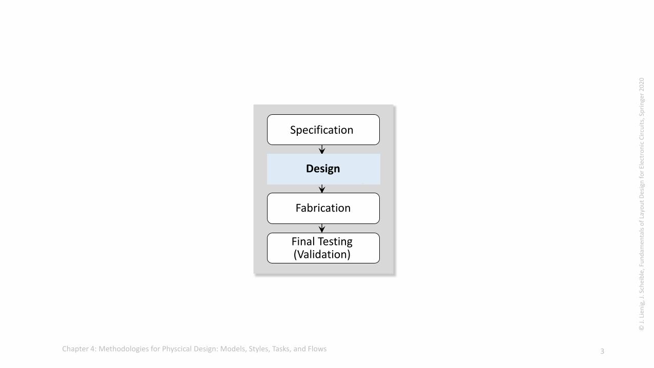
Specification
Design
Final Testing(Validation)
Fabrication
3

© J
. Lie
nig
, J. S
chei
ble
, Fu
nd
amen
tals
of
Layo
ut
Des
ign
fo
rEl
ectr
on
ic C
ircu
its,
Sp
rin
ger
20
20
Chapter 4: Methodologies for Physcical Design: Models, Styles, Tasks, and Flows
Design step
Verification step
While errors
While further design steps
Specification
Fabrication
4
© J
. Lie
nig
, J. S
chei
ble
, Fu
nd
amen
tals
of
Layo
ut
Des
ign
fo
rEl
ectr
on
ic C
ircu
its,
Sp
rin
ger
20
20
Chapter 4: Methodologies for Physcical Design: Models, Styles, Tasks, and Flows
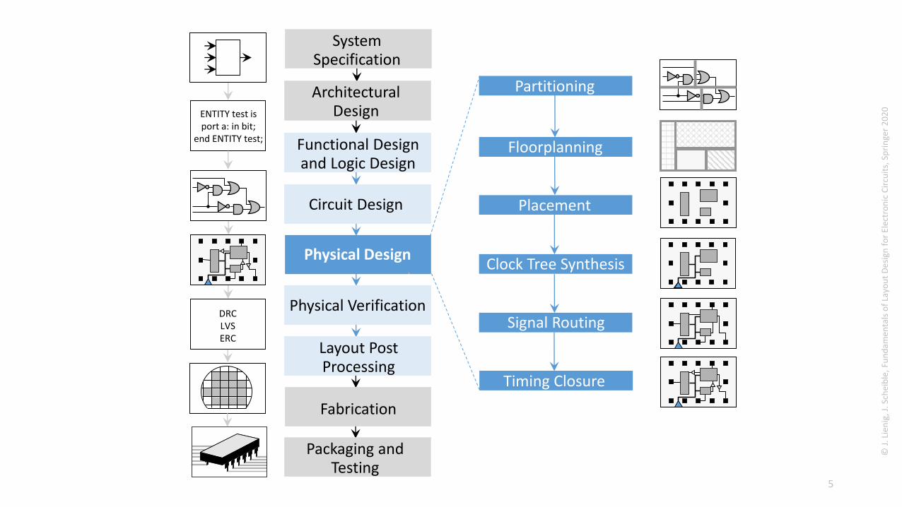
ENTITY test isport a: in bit;
end ENTITY test;
DRCLVSERC
Circuit Design
Functional Designand Logic Design
Physical Design
Physical Verification
Layout Post Processing
SystemSpecification
ArchitecturalDesign
Packaging and Testing
Floorplanning
Placement
Signal Routing
Partitioning
Timing Closure
Clock Tree Synthesis
Fabrication
5

© J
. Lie
nig
, J. S
chei
ble
, Fu
nd
amen
tals
of
Layo
ut
Des
ign
fo
rEl
ectr
on
ic C
ircu
its,
Sp
rin
ger
20
20
Chapter 4: Methodologies for Physcical Design: Models, Styles, Tasks, and Flows
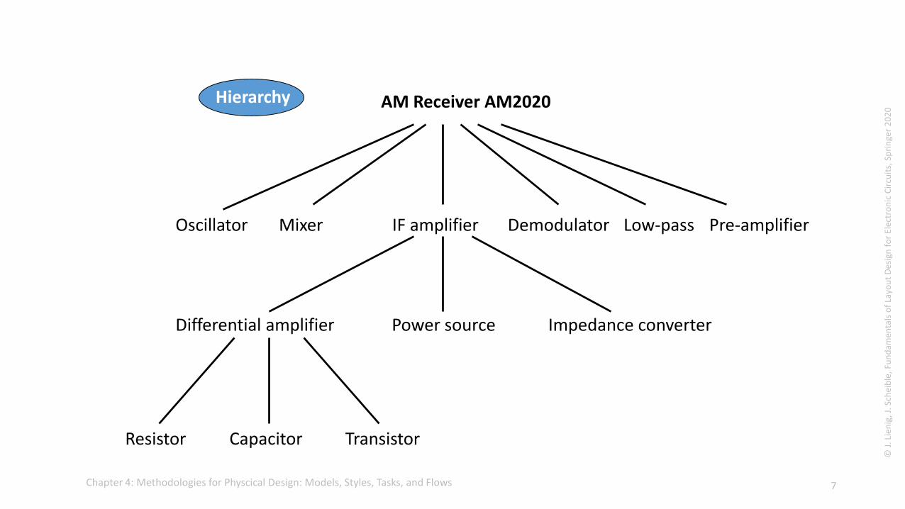
Hierarchy
Version View
Hie
rarc
hy
leve
ls Fully detailed circuit description
General design
Schematic
Layout
1.0
4.1
6
© J
. Lie
nig
, J. S
chei
ble
, Fu
nd
amen
tals
of
Layo
ut
Des
ign
fo
rEl
ectr
on
ic C
ircu
its,
Sp
rin
ger
20
20
Chapter 4: Methodologies for Physcical Design: Models, Styles, Tasks, and Flows
AM Receiver AM2020
Pre-amplifierOscillator Mixer IF amplifier Demodulator Low-pass
Differential amplifier Power source Impedance converter
Resistor Capacitor Transistor
Hierarchy
7

© J
. Lie
nig
, J. S
chei
ble
, Fu
nd
amen
tals
of
Layo
ut
Des
ign
fo
rEl
ectr
on
ic C
ircu
its,
Sp
rin
ger
20
20
Chapter 4: Methodologies for Physcical Design: Models, Styles, Tasks, and Flows
A1
A2
A3
A4
B1
B2
B3 C1 D1
D2
D3
D4C2
AM Receiver AM2020 Version
8
© J
. Lie
nig
, J. S
chei
ble
, Fu
nd
amen
tals
of
Layo
ut
Des
ign
fo
rEl
ectr
on
ic C
ircu
its,
Sp
rin
ger
20
20
Chapter 4: Methodologies for Physcical Design: Models, Styles, Tasks, and Flows
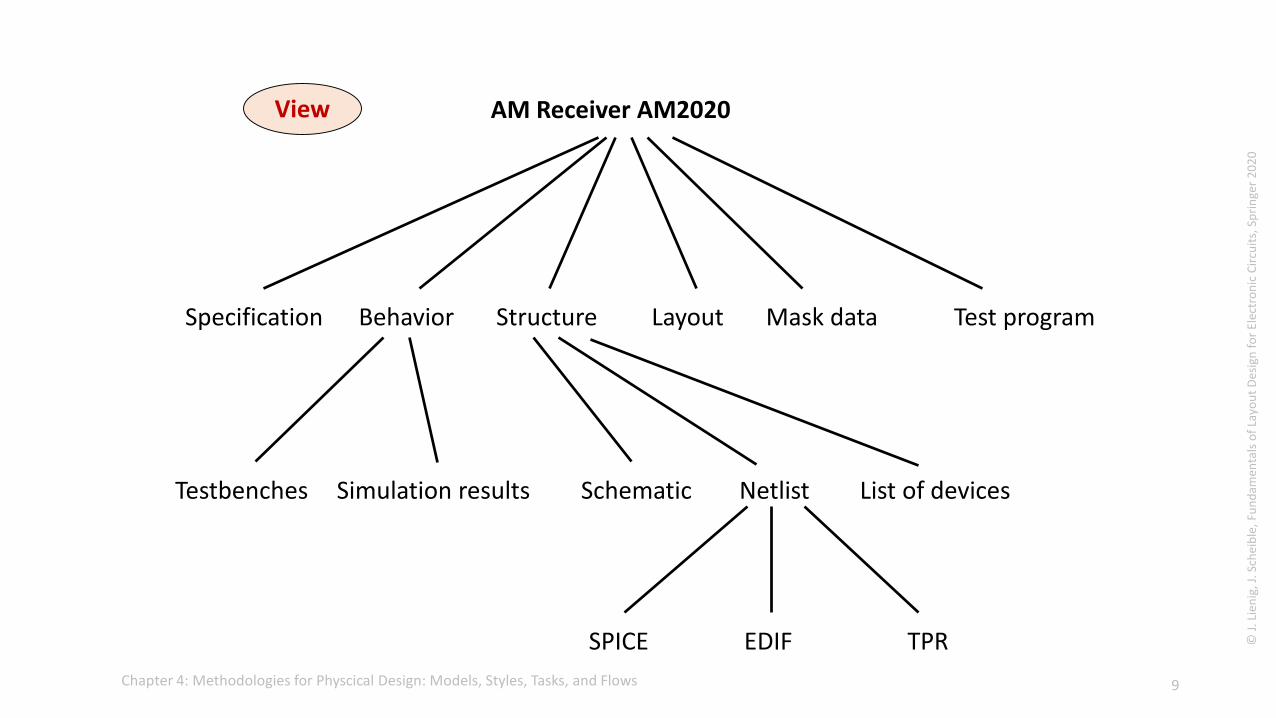
Specification Behavior Structure Layout Mask data Test program
SPICE EDIF TPR
AM Receiver AM2020
Schematic Netlist List of devicesSimulation results
View
Testbenches
9
© J
. Lie
nig
, J. S
chei
ble
, Fu
nd
amen
tals
of
Layo
ut
Des
ign
fo
rEl
ectr
on
ic C
ircu
its,
Sp
rin
ger
20
20
Chapter 4: Methodologies for Physcical Design: Models, Styles, Tasks, and Flows
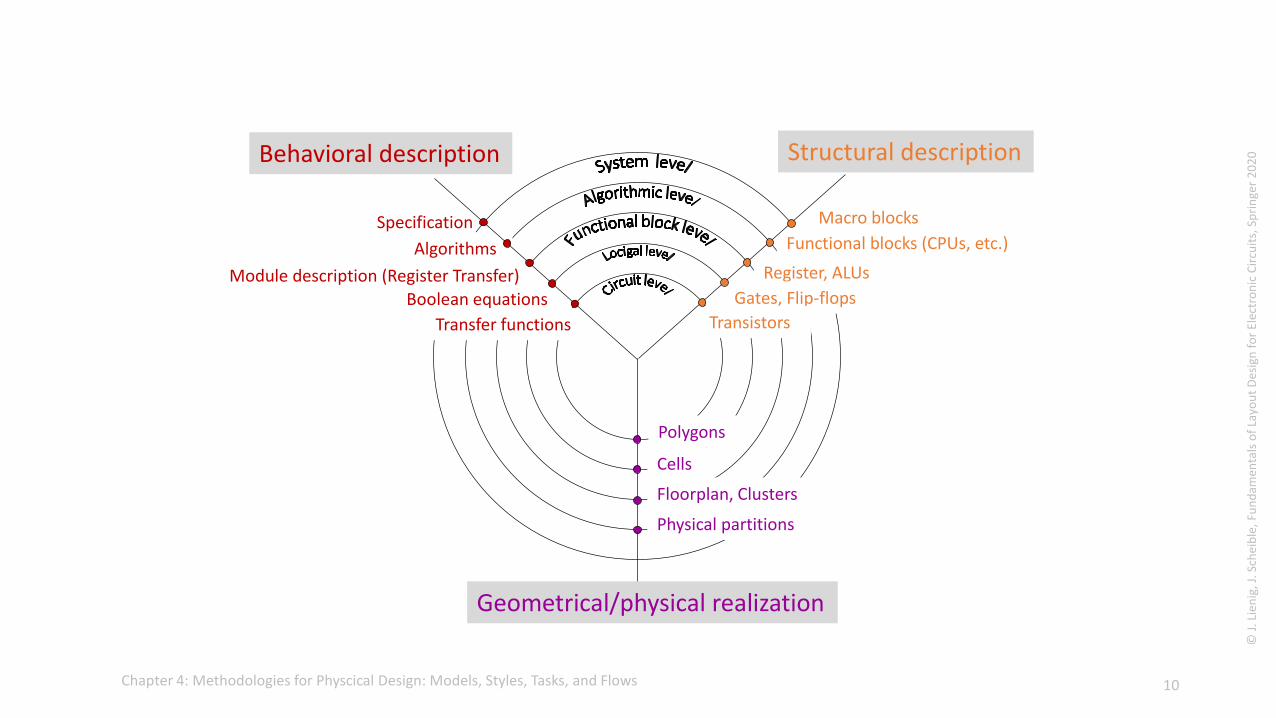
Geometrical/physical realization
Structural descriptionBehavioral description
Specification
Algorithms
Boolean equations
Physical partitions
Floorplan, Clusters
Cells
Polygons
Functional blocks (CPUs, etc.)
Register, ALUs
Gates, Flip-flops
Transistors
Macro blocks
Module description (Register Transfer)
Transfer functions
10
© J
. Lie
nig
, J. S
chei
ble
, Fu
nd
amen
tals
of
Layo
ut
Des
ign
fo
rEl
ectr
on
ic C
ircu
its,
Sp
rin
ger
20
20
Chapter 4: Methodologies for Physcical Design: Models, Styles, Tasks, and Flows
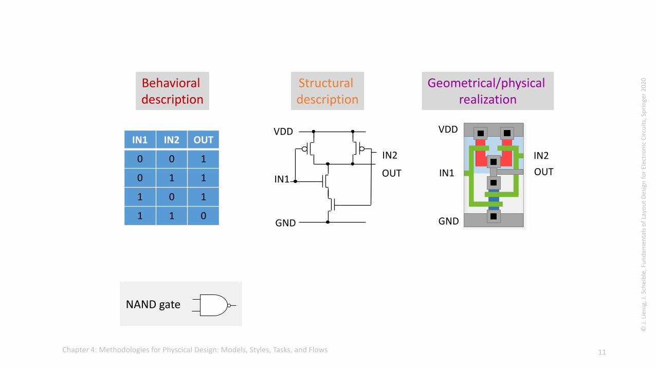
OUTIN1
VDD
GND
IN2
IN1
VDD
GND
OUT
IN2
IN1 IN2 OUT
0 0 1
0 1 1
1 0 1
1 1 0
Geometrical/physical realization
Structural description
Behavioral description
11
NAND gate

© J
. Lie
nig
, J. S
chei
ble
, Fu
nd
amen
tals
of
Layo
ut
Des
ign
fo
rEl
ectr
on
ic C
ircu
its,
Sp
rin
ger
20
20
Chapter 4: Methodologies for Physcical Design: Models, Styles, Tasks, and Flows
Geometry
StructureBehavior
Macro blocks
Functional blocks (CPUs, etc.)
Register, ALUs
Gates Flip-flops
Transistors
Specification
Algorithms
Module description (RTL)
Boolean equations
Transfer functions
Physical partitions
Floorplan, Clusters
Cells
Polygons
Circuit synthesisLogic synthesis
Behavioral synthesis
Layout generators
Geometry
StructureBehavior
Macro blocks
Functional blocks (CPUs, etc.)
Register, ALUs
Gates, Flip-flops
Transistors
Specification
Algorithms
Module description (RTL)
Boolean equations
Transfer functions
Physical partitions
Floorplan, Clusters
Cells
PolygonsLayout design
Transistor design
Logic designSystem design
12
© J
. Lie
nig
, J. S
chei
ble
, Fu
nd
amen
tals
of
Layo
ut
Des
ign
fo
rEl
ectr
on
ic C
ircu
its,
Sp
rin
ger
20
20
Chapter 4: Methodologies for Physcical Design: Models, Styles, Tasks, and Flows
INV NORNAND
OUTIN1
VDD
GND
IN2
OUTIN
VDD
GND
OUTIN1
VDD
GND
IN2
Contact layer
n+-doping layer
Metal layer
Poly layer
Transistor
p+-doping layer
n--doping layer
13
© J
. Lie
nig
, J. S
chei
ble
, Fu
nd
amen
tals
of
Layo
ut
Des
ign
fo
rEl
ectr
on
ic C
ircu
its,
Sp
rin
ger
20
20
Chapter 4: Methodologies for Physcical Design: Models, Styles, Tasks, and Flows
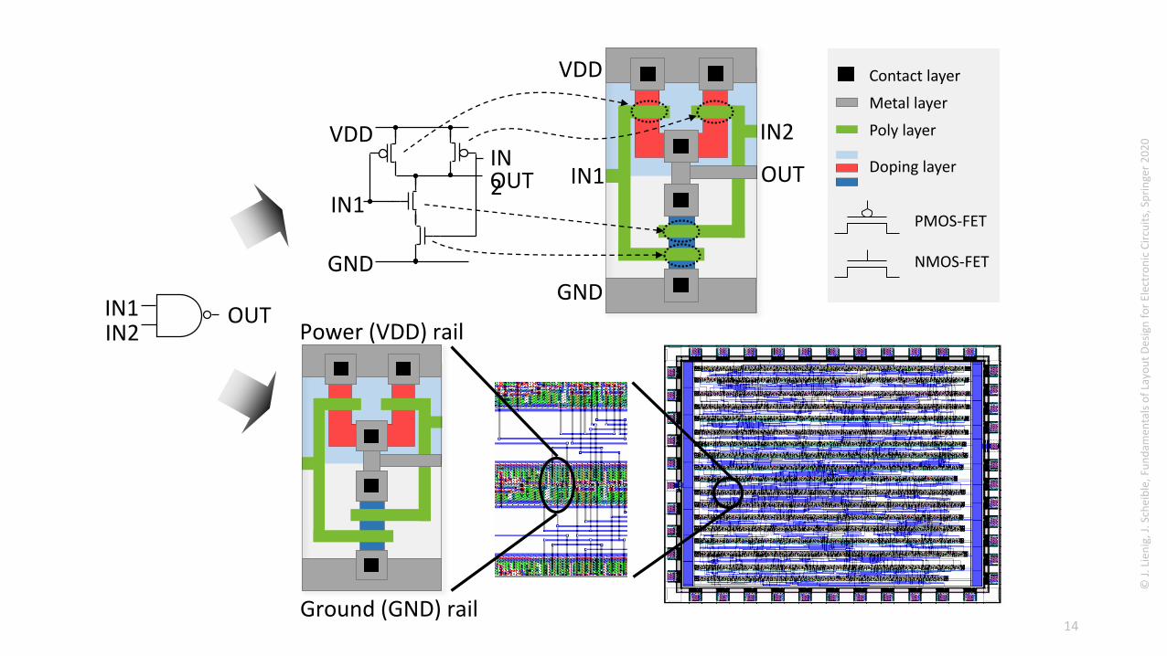
Power (VDD) rail
Ground (GND) rail
Contact layer
VDD
GND
OUTIN2
IN1 OUTIN2
IN1
OUTIN1
VDD
GND
IN2
Doping layer
Metal layer
Poly layer
PMOS-FET
NMOS-FET
14

© J
. Lie
nig
, J. S
chei
ble
, Fu
nd
amen
tals
of
Layo
ut
Des
ign
fo
rEl
ectr
on
ic C
ircu
its,
Sp
rin
ger
20
20
Chapter 4: Methodologies for Physcical Design: Models, Styles, Tasks, and Flows
A
VDD
Feedthroughcell
Pad
Groundpad
Routing channel
Standard cells
Power pad VDD
Pad
Groundpad
Standard cells
Power pad
A’
A
A’GNDGND
15

© J
. Lie
nig
, J. S
chei
ble
, Fu
nd
amen
tals
of
Layo
ut
Des
ign
fo
rEl
ectr
on
ic C
ircu
its,
Sp
rin
ger
20
20
Chapter 4: Methodologies for Physcical Design: Models, Styles, Tasks, and Flows
Pad
GND
VDD
PLA RAM
Standard cell block
RAM
PLA
Routing regions
Groundpad
Power pad
16

© J
. Lie
nig
, J. S
chei
ble
, Fu
nd
amen
tals
of
Layo
ut
Des
ign
fo
rEl
ectr
on
ic C
ircu
its,
Sp
rin
ger
20
20
Chapter 4: Methodologies for Physcical Design: Models, Styles, Tasks, and Flows
GND
VDD
Switchbox
Vertical channel
Horizontal channel
Pad
Groundpad
Power pad
17

© J
. Lie
nig
, J. S
chei
ble
, Fu
nd
amen
tals
of
Layo
ut
Des
ign
fo
rEl
ectr
on
ic C
ircu
its,
Sp
rin
ger
20
20
Chapter 4: Methodologies for Physcical Design: Models, Styles, Tasks, and Flows
LB LB LB
SB SB
LB LB LB
SB SB
LB LB LB
LB LE LB
SB SB
LB LB LB
SB SB
LB LB LB
LE LE
SB SB
LE LE LE
SB SB
LE LE LE
Cell, logic element
Switchbox Connection
LE
18

© J
. Lie
nig
, J. S
chei
ble
, Fu
nd
amen
tals
of
Layo
ut
Des
ign
fo
rEl
ectr
on
ic C
ircu
its,
Sp
rin
ger
20
20
Chapter 4: Methodologies for Physcical Design: Models, Styles, Tasks, and Flows
Design style Design cost Mask cost Fab cost PerformanceEconomicvolume
Full custom High High Low High High
Standard cell Low High Medium Medium Wide range
Macro cellHigh Low (reuse)
High Low High Wide range
Gate array Low Medium High Low Low
FPGA Very low None High Low Low
19
© J
. Lie
nig
, J. S
chei
ble
, Fu
nd
amen
tals
of
Layo
ut
Des
ign
fo
rEl
ectr
on
ic C
ircu
its,
Sp
rin
ger
20
20
Chapter 4: Methodologies for Physcical Design: Models, Styles, Tasks, and Flows
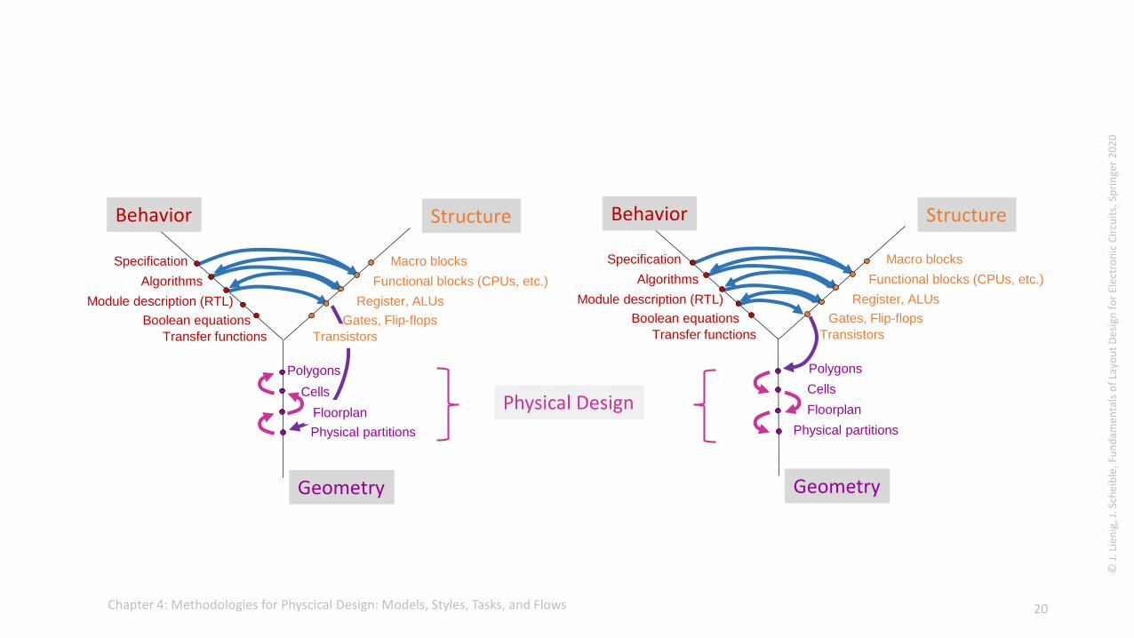
Geometry
StructureBehavior
Macro blocks
Functional blocks (CPUs, etc.)
Register, ALUs
Gates, Flip-flops
Transistors
Specification
Algorithms
Module description (RTL)
Boolean equations
Transfer functions
Physical partitions
Floorplan
Cells
Polygons
Geometry
StructureBehavior
Macro blocks
Functional blocks (CPUs, etc.)
Register, ALUs
Specification
Algorithms
Module description (RTL)
Boolean equations
Transfer functions
Physical partitions
Cells
Polygons
Floorplan
Transistors
Gates, Flip-flops
Physical Design
20

© J
. Lie
nig
, J. S
chei
ble
, Fu
nd
amen
tals
of
Layo
ut
Des
ign
fo
rEl
ectr
on
ic C
ircu
its,
Sp
rin
ger
20
20
Chapter 4: Methodologies for Physcical Design: Models, Styles, Tasks, and Flows
Problem
Formalization
Implementation
Verification
Validation
Has the correct circuit been designed?
Has the circuit been correctly designed?
Specification Product
21

© J
. Lie
nig
, J. S
chei
ble
, Fu
nd
amen
tals
of
Layo
ut
Des
ign
fo
rEl
ectr
on
ic C
ircu
its,
Sp
rin
ger
20
20
Chapter 4: Methodologies for Physcical Design: Models, Styles, Tasks, and Flows
Circuit Design
Physical Designand Verification
Fabrication
Specification Technology data
Layout Post Processing
Design data
Geometrical
design
rules
Technological
constraints
Functional
(electrical)
constraints
Design-
methodology
(geometry)
constraints
22

© J
. Lie
nig
, J. S
chei
ble
, Fu
nd
amen
tals
of
Layo
ut
Des
ign
fo
rEl
ectr
on
ic C
ircu
its,
Sp
rin
ger
20
20
Chapter 4: Methodologies for Physcical Design: Models, Styles, Tasks, and Flows
t
Out (V)
t
Out (V)
t
´1´
´0´
t
´1´
´0´
Digital Analog
„Inverter“
Rise time
OutDriver Load
Forbidden voltage range
Forbidden time range
Out (V)
23
© J
. Lie
nig
, J. S
chei
ble
, Fu
nd
amen
tals
of
Layo
ut
Des
ign
fo
rEl
ectr
on
ic C
ircu
its,
Sp
rin
ger
20
20
Chapter 4: Methodologies for Physcical Design: Models, Styles, Tasks, and Flows
Geometrical/physical realization
Specification
Algorithms
Boolean equations
Physical partitions
Floorplan, Clusters
Cells
Polygons
Geometrical/physical realization
Block diagram
Schematic, circuit diagram
Device symbolsPins, diffusion areas
Functional description
Characteristic curve, transfer function
Models Differential functions
Floorplan
Blocks
Devices, device generators
Polygons
Digital Analog
Functional blocks (CPUs, etc.)
Register, ALUsGates, Flip-flops
Transistors
Macro blocks
Module description (RTL)
Transfer functions
Structuraldescription
Behavioraldescription
Structuraldescription
Behavioraldescription
24
© J
. Lie
nig
, J. S
chei
ble
, Fu
nd
amen
tals
of
Layo
ut
Des
ign
fo
rEl
ectr
on
ic C
ircu
its,
Sp
rin
ger
20
20
Chapter 4: Methodologies for Physcical Design: Models, Styles, Tasks, and Flows
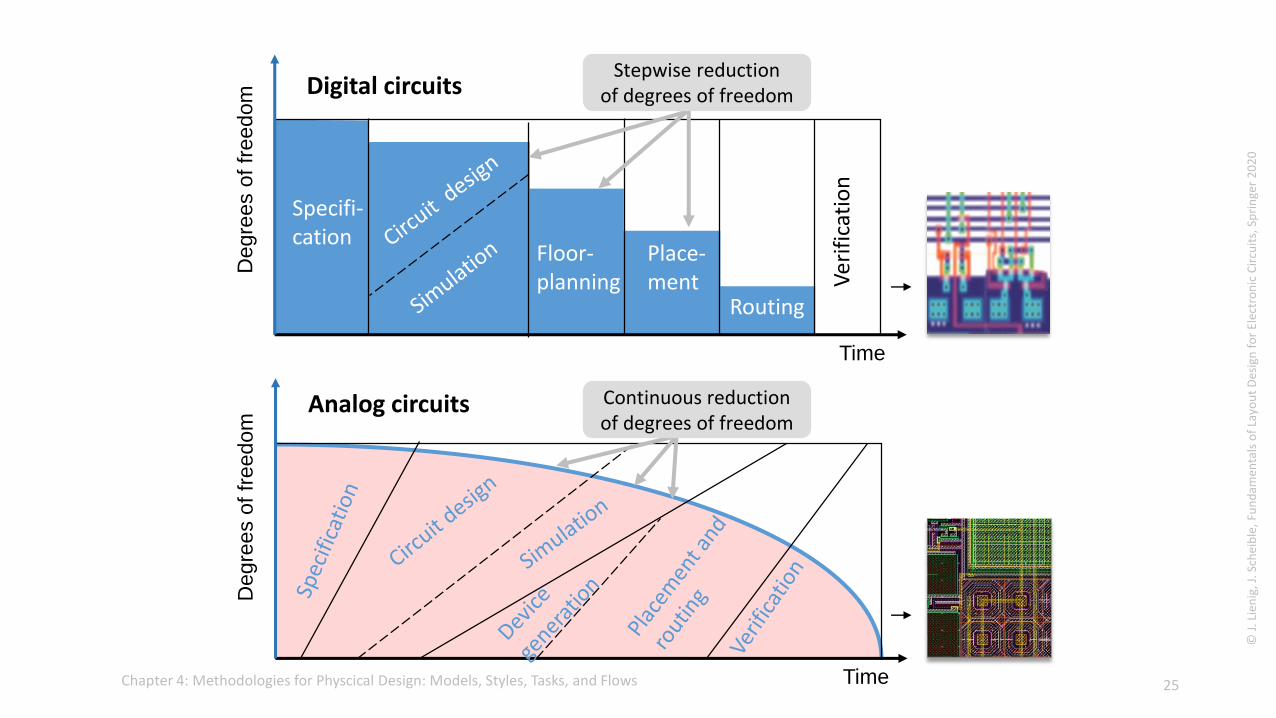
Specifi-cation
Floor-planning
Place-ment
Routing
Ver
ific
atio
n
Degre
es
of
freedom Digital circuits
Degre
es
of
freedom
Analog circuits
Time
Time
Stepwise reductionof degrees of freedom
Continuous reductionof degrees of freedom
25

© J
. Lie
nig
, J. S
chei
ble
, Fu
nd
amen
tals
of
Layo
ut
Des
ign
fo
rEl
ectr
on
ic C
ircu
its,
Sp
rin
ger
20
20
Chapter 4: Methodologies for Physcical Design: Models, Styles, Tasks, and Flows
Minimum requiredautomation fordigital problems
Efficiency ofoptimizingalgorithms
Accuracy ofmathematicalmodelling
Digital design problems madeautomatable by standardization
Minimum required accuracyfor analog problems
Design problemsnot solvable
by optimizers
Design problemssolvable by optimizers
lie beyond theoptimization horizon
Digital design problems
Analog design problems
26

© J
. Lie
nig
, J. S
chei
ble
, Fu
nd
amen
tals
of
Layo
ut
Des
ign
fo
rEl
ectr
on
ic C
ircu
its,
Sp
rin
ger
20
20
Chapter 4: Methodologies for Physcical Design: Models, Styles, Tasks, and Flows
Exploration engine
Evaluation engine
CandidateSelection
EDA expertknowledge
Objectives,constraints
Layout expertknowledge
Layout“solutionˮ
Top-Down Design „Optimizing Approach“
Bottom-Up Design „Procedural Approach“
Layout“resultˮ
Layoutproblem
Layoutproblem
Solution strategy, implicit constraints
Optimizer Procedure
ParametersLayout expertknowledge
27

© J
. Lie
nig
, J. S
chei
ble
, Fu
nd
amen
tals
of
Layo
ut
Des
ign
fo
rEl
ectr
on
ic C
ircu
its,
Sp
rin
ger
20
20
Chapter 4: Methodologies for Physcical Design: Models, Styles, Tasks, and Flows
Synthesis Steps
Logic SynthesisPartitioningFloorplanningPower RoutingGlobal PlacementDetailed PlacementClock Tree SynthesisGlobal RoutingDetailed RoutingTiming Closure
Analysis / Verification Steps
Formal Verification
Global Timing
Routability Prediction
Timing
Parasitic ExtractionSign-off DRCSign-off TimingSign-off Spice Simulation
28
© J
. Lie
nig
, J. S
chei
ble
, Fu
nd
amen
tals
of
Layo
ut
Des
ign
fo
rEl
ectr
on
ic C
ircu
its,
Sp
rin
ger
20
20
Chapter 4: Methodologies for Physcical Design: Models, Styles, Tasks, and Flows
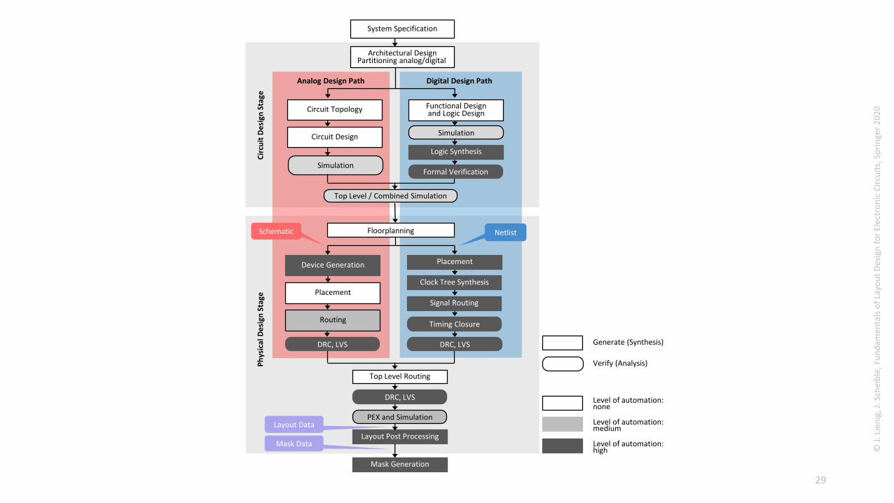
Architectural DesignPartitioning analog/digital
System Specification
Cir
cuit
De
sign
Sta
geP
hys
ical
De
sign
Sta
ge
Simulation
Top Level / Combined Simulation
Analog Design Path Digital Design Path
Circuit Topology
Circuit Design
Logic Synthesis
Simulation
Formal Verification
Floorplanning
Layout Post Processing
Mask Generation
PEX and Simulation
Top Level Routing
DRC, LVS
Schematic Netlist
Generate (Synthesis)
Verify (Analysis)
Level of automation: none
Level of automation: medium
Level of automation: high
Device Generation
Placement
Routing
DRC, LVS
Placement
Clock Tree Synthesis
Signal Routing
Timing Closure
DRC, LVS
Functional Design and Logic Design
Layout Data
Mask Data
29
© J
. Lie
nig
, J. S
chei
ble
, Fu
nd
amen
tals
of
Layo
ut
Des
ign
fo
rEl
ectr
on
ic C
ircu
its,
Sp
rin
ger
20
20
Chapter 4: Methodologies for Physcical Design: Models, Styles, Tasks, and Flows
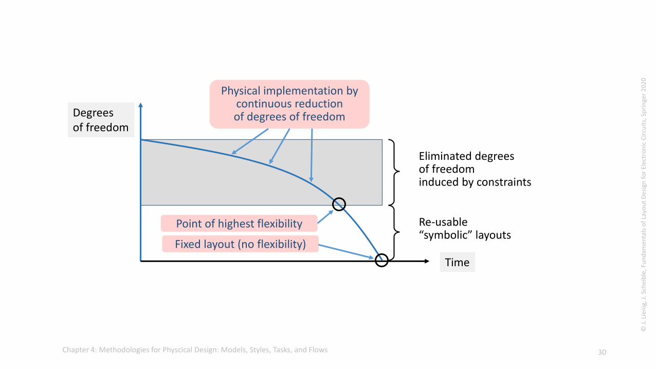
Degreesof freedom
Time
Eliminated degreesof freedominduced by constraints
Re-usable “symbolic” layouts
Physical implementation bycontinuous reductionof degrees of freedom
Point of highest flexibility
Fixed layout (no flexibility)
30
© J
. Lie
nig
, J. S
chei
ble
, Fu
nd
amen
tals
of
Layo
ut
Des
ign
fo
rEl
ectr
on
ic C
ircu
its,
Sp
rin
ger
20
20
Chapter 4: Methodologies for Physcical Design: Models, Styles, Tasks, and Flows
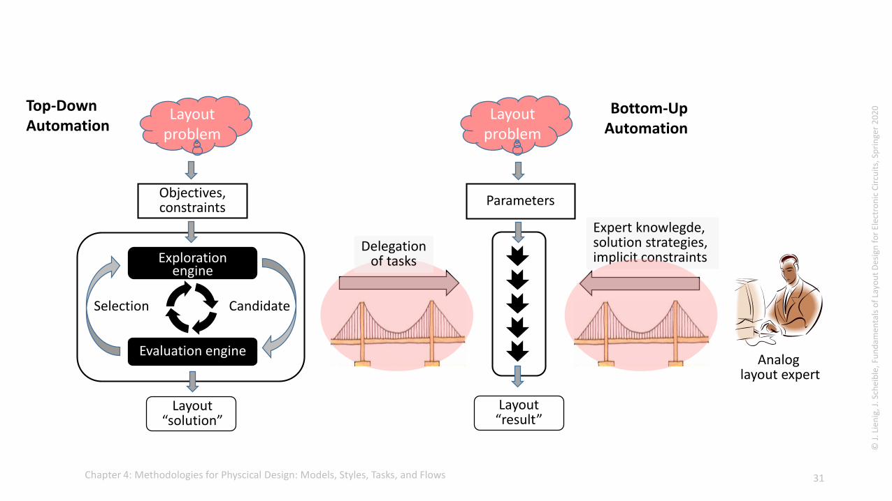
Analog layout expert
Exploration engine
Evaluation engine
CandidateSelection
Objectives,constraints
Layout“solution”
Layout“result”
Parameters
Delegationof tasks
Expert knowlegde,solution strategies, implicit constraints
Top-DownAutomation
Bottom-UpAutomation
Layoutproblem
Layoutproblem
31