chapter 6€¦ · figure 6.4 structure of a vector unit containing four lanes. the vector-register...
TRANSCRIPT

Chapter 6
Parallel Processors from Client to
Cloud
Copyright © 2014 Elsevier Inc. All rights reserved.

2 Copyright © 2014 Elsevier Inc. All rights reserved.
FIGURE 6.1 Hardware/software categorization and examples of application perspective on concurrency versus
hardware perspective on parallelism.

3 Copyright © 2014 Elsevier Inc. All rights reserved.
FIGURE 6.2 Hardware categorization and examples based on number of instruction streams and data streams:
SISD, SIMD, MISD, and MIMD.
4 Copyright © 2014 Elsevier Inc. All rights reserved.
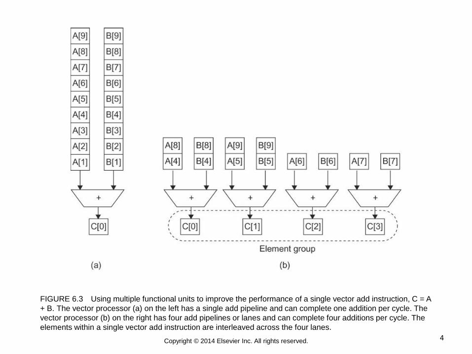
FIGURE 6.3 Using multiple functional units to improve the performance of a single vector add instruction, C = A
+ B. The vector processor (a) on the left has a single add pipeline and can complete one addition per cycle. The
vector processor (b) on the right has four add pipelines or lanes and can complete four additions per cycle. The
elements within a single vector add instruction are interleaved across the four lanes.

5 Copyright © 2014 Elsevier Inc. All rights reserved.
FIGURE 6.4 Structure of a vector unit containing four lanes. The vector-register storage is divided across the
lanes, with each lane holding every fourth element of each vector register. The figure shows three vector
functional units: an FP add, an FP multiply, and a load-store unit. Each of the vector arithmetic units contains
four execution pipelines, one per lane, which acts in concert to complete a single vector instruction. Note how
each section of the vector-register file only needs to provide enough read and write ports (see Chapter 4) for
functional units local to its lane.

6 Copyright © 2014 Elsevier Inc. All rights reserved.
FIGURE 6.5 How four threads use the issue slots of a superscalar processor in different approaches. The four
threads at the top show how each would execute running alone on a standard superscalar processor without
multithreading support. The three examples at the bottom show how they would execute running together in
three multithreading options. The horizontal dimension represents the instruction issue capability in each clock
cycle. The vertical dimension represents a sequence of clock cycles. An empty (white) box indicates that the
corresponding issue slot is unused in that clock cycle. The shades of gray and color correspond to four different
threads in the multithreading processors. The additional pipeline start-up effects for coarse multithreading, which
are not illustrated in this figure, would lead to further loss in throughput for coarse multithreading.
7 Copyright © 2014 Elsevier Inc. All rights reserved.
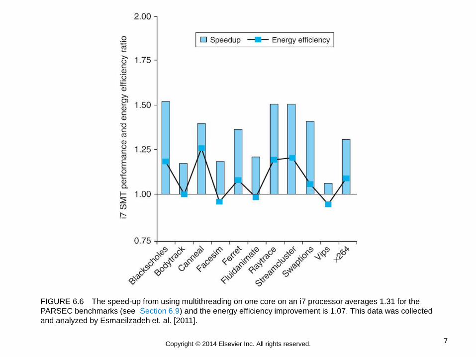
FIGURE 6.6 The speed-up from using multithreading on one core on an i7 processor averages 1.31 for the
PARSEC benchmarks (see Section 6.9) and the energy efficiency improvement is 1.07. This data was collected
and analyzed by Esmaeilzadeh et. al. [2011].
8 Copyright © 2014 Elsevier Inc. All rights reserved.
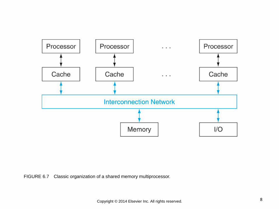
FIGURE 6.7 Classic organization of a shared memory multiprocessor.

9 Copyright © 2014 Elsevier Inc. All rights reserved.
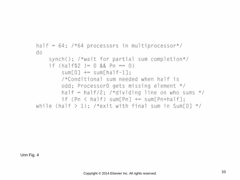
FIGURE 6.8 The last four levels of a reduction that sums results from each processor, from bottom to top. For
all processors whose number i is less than half, add the sum produced by processor number (i + half) to its sum.
10 Copyright © 2014 Elsevier Inc. All rights reserved.
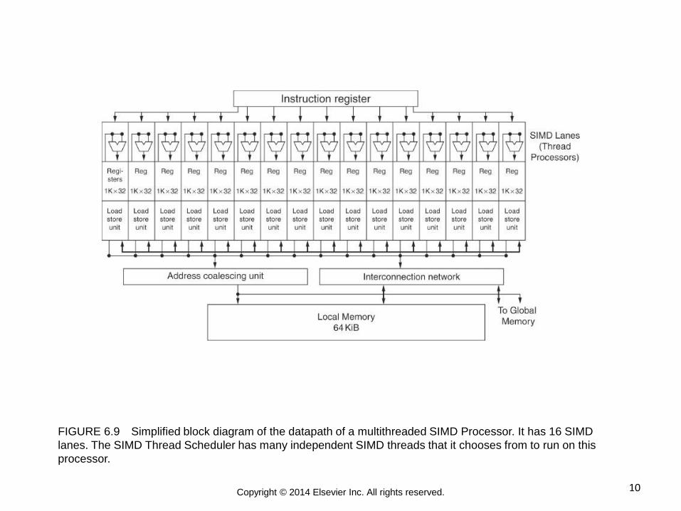
FIGURE 6.9 Simplified block diagram of the datapath of a multithreaded SIMD Processor. It has 16 SIMD
lanes. The SIMD Thread Scheduler has many independent SIMD threads that it chooses from to run on this
processor.

11 Copyright © 2014 Elsevier Inc. All rights reserved.
FIGURE 6.10 GPU Memory structures. GPU Memory is shared by the vectorized loops. All threads of SIMD
instructions within a thread block share Local Memory.

12 Copyright © 2014 Elsevier Inc. All rights reserved.
FIGURE 6.11 Similarities and differences between multicore with Multimedia SIMD extensions and recent
GPUs.
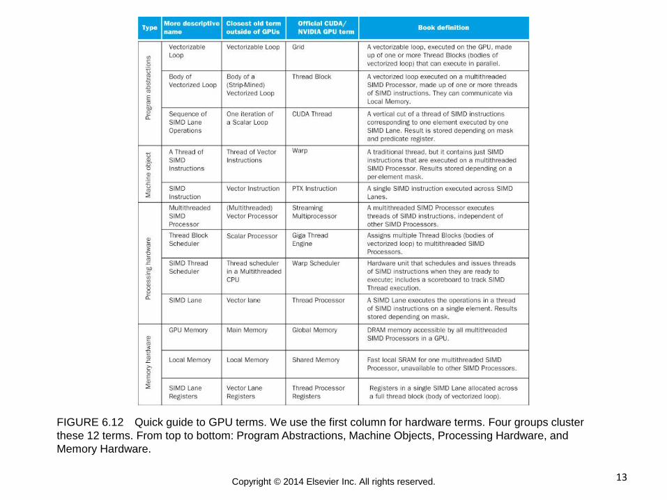
13 Copyright © 2014 Elsevier Inc. All rights reserved.
FIGURE 6.12 Quick guide to GPU terms. We use the first column for hardware terms. Four groups cluster
these 12 terms. From top to bottom: Program Abstractions, Machine Objects, Processing Hardware, and
Memory Hardware.
14 Copyright © 2014 Elsevier Inc. All rights reserved.
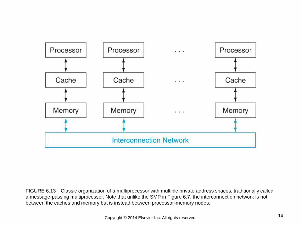
FIGURE 6.13 Classic organization of a multiprocessor with multiple private address spaces, traditionally called
a message-passing multiprocessor. Note that unlike the SMP in Figure 6.7, the interconnection network is not
between the caches and memory but is instead between processor-memory nodes.

15 Copyright © 2014 Elsevier Inc. All rights reserved.
FIGURE 6.14 Network topologies that have appeared in commercial parallel processors. The colored circles
represent switches and the black squares represent processor-memory nodes. Even though a switch has many
links, generally only one goes to the processor. The Boolean n-cube topology is an n-dimensional interconnect
with 2n nodes, requiring n links per switch (plus one for the processor) and thus n nearest-neighbor nodes.
Frequently, these basic topologies have been supplemented with extra arcs to improve performance and
reliability.
16 Copyright © 2014 Elsevier Inc. All rights reserved.
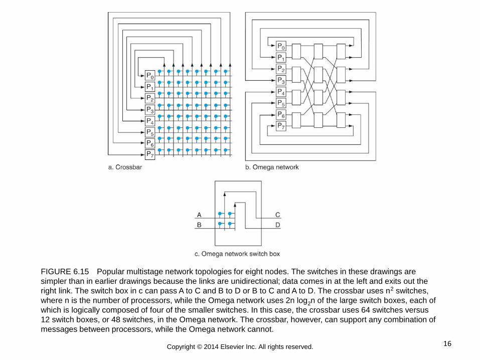
FIGURE 6.15 Popular multistage network topologies for eight nodes. The switches in these drawings are
simpler than in earlier drawings because the links are unidirectional; data comes in at the left and exits out the
right link. The switch box in c can pass A to C and B to D or B to C and A to D. The crossbar uses n2 switches,
where n is the number of processors, while the Omega network uses 2n log2n of the large switch boxes, each of
which is logically composed of four of the smaller switches. In this case, the crossbar uses 64 switches versus
12 switch boxes, or 48 switches, in the Omega network. The crossbar, however, can support any combination of
messages between processors, while the Omega network cannot.

17 Copyright © 2014 Elsevier Inc. All rights reserved.
FIGURE 6.16 Examples of parallel benchmarks.

18 Copyright © 2014 Elsevier Inc. All rights reserved.
FIGURE 6.17 Arithmetic intensity, specified as the number of float-point operations to run the program divided
by the number of bytes accessed in main memory [Williams, Waterman, and Patterson 2009]. Some kernels
have an arithmetic intensity that scales with problem size, such as Dense Matrix, but there are many kernels with
arithmetic intensities independent of problem size. For kernels in this former case, weak scaling can lead to
different results, since it puts much less demand on the memory system.
19 Copyright © 2014 Elsevier Inc. All rights reserved.
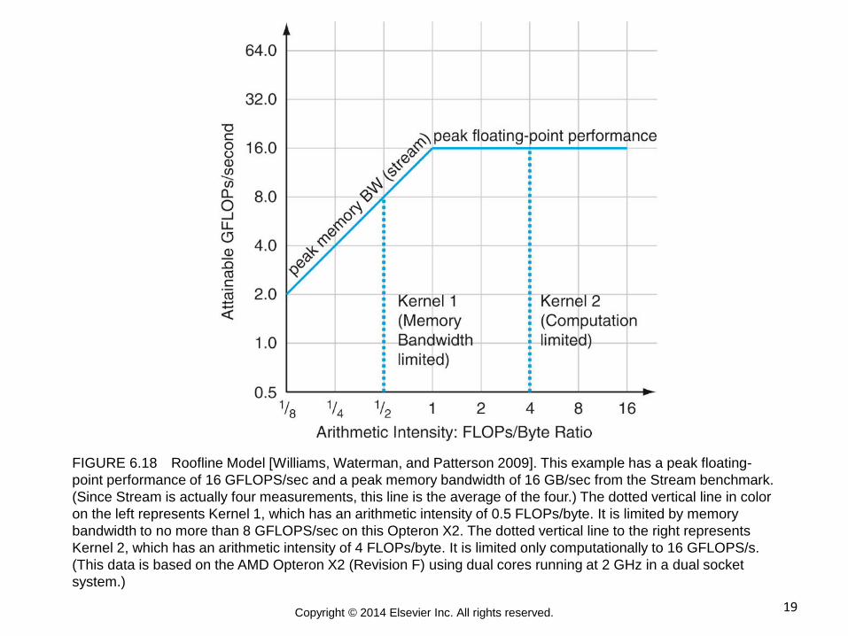
FIGURE 6.18 Roofline Model [Williams, Waterman, and Patterson 2009]. This example has a peak floating-
point performance of 16 GFLOPS/sec and a peak memory bandwidth of 16 GB/sec from the Stream benchmark.
(Since Stream is actually four measurements, this line is the average of the four.) The dotted vertical line in color
on the left represents Kernel 1, which has an arithmetic intensity of 0.5 FLOPs/byte. It is limited by memory
bandwidth to no more than 8 GFLOPS/sec on this Opteron X2. The dotted vertical line to the right represents
Kernel 2, which has an arithmetic intensity of 4 FLOPs/byte. It is limited only computationally to 16 GFLOPS/s.
(This data is based on the AMD Opteron X2 (Revision F) using dual cores running at 2 GHz in a dual socket
system.)
20 Copyright © 2014 Elsevier Inc. All rights reserved.
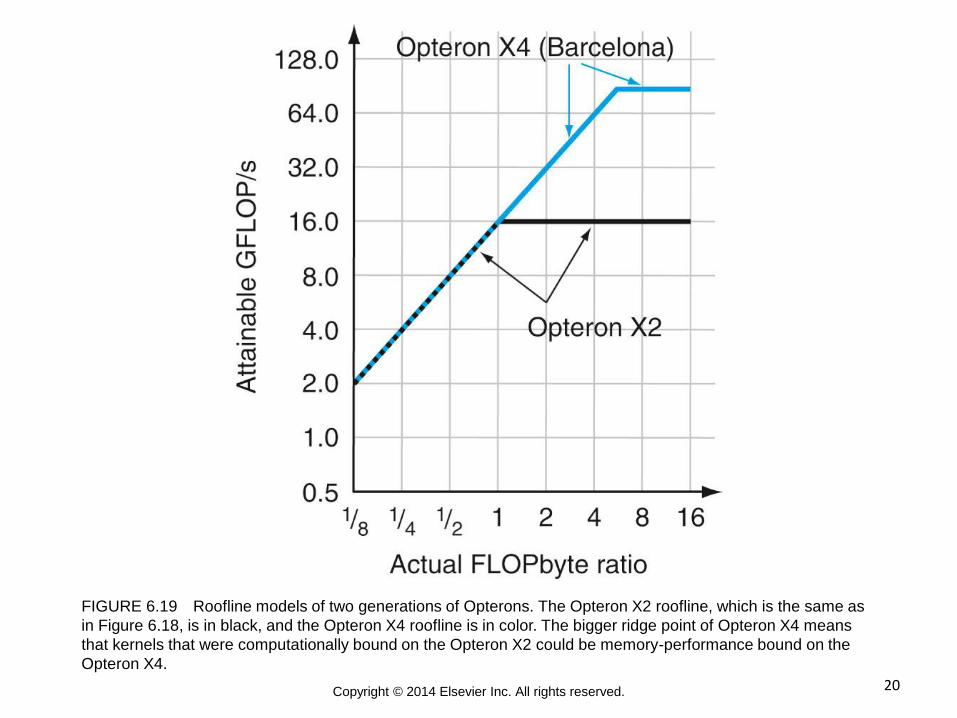
FIGURE 6.19 Roofline models of two generations of Opterons. The Opteron X2 roofline, which is the same as
in Figure 6.18, is in black, and the Opteron X4 roofline is in color. The bigger ridge point of Opteron X4 means
that kernels that were computationally bound on the Opteron X2 could be memory-performance bound on the
Opteron X4.
21 Copyright © 2014 Elsevier Inc. All rights reserved.
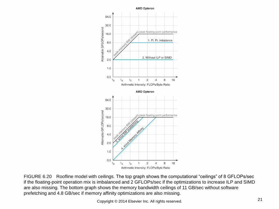
FIGURE 6.20 Roofline model with ceilings. The top graph shows the computational “ceilings” of 8 GFLOPs/sec
if the floating-point operation mix is imbalanced and 2 GFLOPs/sec if the optimizations to increase ILP and SIMD
are also missing. The bottom graph shows the memory bandwidth ceilings of 11 GB/sec without software
prefetching and 4.8 GB/sec if memory affinity optimizations are also missing.

22 Copyright © 2014 Elsevier Inc. All rights reserved.
FIGURE 6.21 Roofline model with ceilings, overlapping areas shaded, and the two kernels from Figure 6.18.
Kernels whose arithmetic intensity land in the blue trapezoid on the right should focus on computation
optimizations, and kernels whose arithmetic intensity land in the gray triangle in the lower left should focus on
memory bandwidth optimizations. Those that land in the blue-gray parallelogram in the middle need to worry
about both. As Kernel 1 falls in the parallelogram in the middle, try optimizing ILP and SIMD, memory affinity, and
software prefetching. Kernel 2 falls in the trapezoid on the right, so try optimizing ILP and SIMD and the balance
of floating-point operations.

23 Copyright © 2014 Elsevier Inc. All rights reserved.
FIGURE 6.22 Intel Core i7-960, NVIDIA GTX 280, and GTX 480 specifications. The rightmost columns show
the ratios of the Tesla GTX 280 and the Fermi GTX 480 to Core i7. Although the case study is between the Tesla
280 and i7, we include the Fermi 480 to show its relationship to the Tesla 280 since it is described in this chapter.
Note that these memory bandwidths are higher than in Figure 6.23 because these are DRAM pin bandwidths
and those in Figure 6.23 are at the processors as measured by a benchmark program. (From Table 2 in Lee et
al. [2010].)
24 Copyright © 2014 Elsevier Inc. All rights reserved.
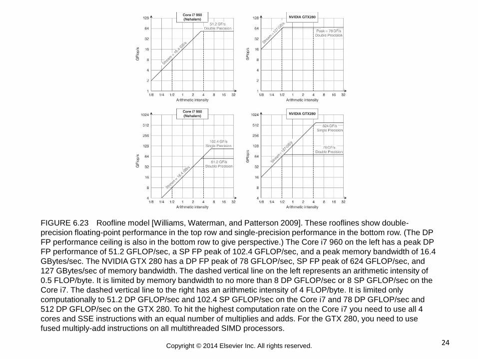
FIGURE 6.23 Roofline model [Williams, Waterman, and Patterson 2009]. These rooflines show double-
precision floating-point performance in the top row and single-precision performance in the bottom row. (The DP
FP performance ceiling is also in the bottom row to give perspective.) The Core i7 960 on the left has a peak DP
FP performance of 51.2 GFLOP/sec, a SP FP peak of 102.4 GFLOP/sec, and a peak memory bandwidth of 16.4
GBytes/sec. The NVIDIA GTX 280 has a DP FP peak of 78 GFLOP/sec, SP FP peak of 624 GFLOP/sec, and
127 GBytes/sec of memory bandwidth. The dashed vertical line on the left represents an arithmetic intensity of
0.5 FLOP/byte. It is limited by memory bandwidth to no more than 8 DP GFLOP/sec or 8 SP GFLOP/sec on the
Core i7. The dashed vertical line to the right has an arithmetic intensity of 4 FLOP/byte. It is limited only
computationally to 51.2 DP GFLOP/sec and 102.4 SP GFLOP/sec on the Core i7 and 78 DP GFLOP/sec and
512 DP GFLOP/sec on the GTX 280. To hit the highest computation rate on the Core i7 you need to use all 4
cores and SSE instructions with an equal number of multiplies and adds. For the GTX 280, you need to use
fused multiply-add instructions on all multithreaded SIMD processors.
25 Copyright © 2014 Elsevier Inc. All rights reserved.
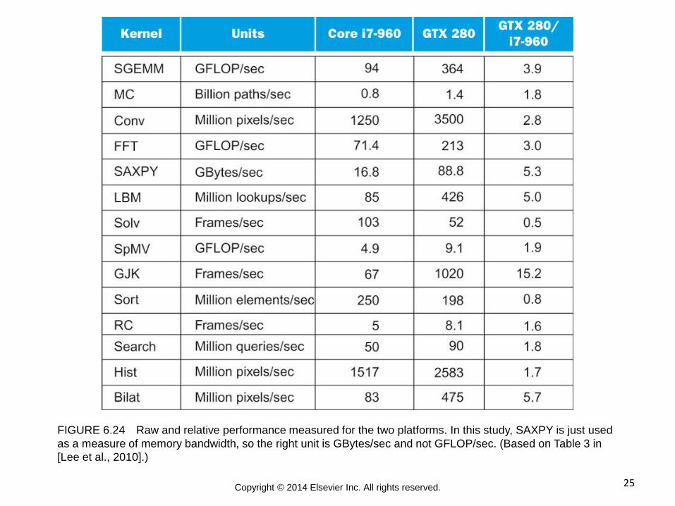
FIGURE 6.24 Raw and relative performance measured for the two platforms. In this study, SAXPY is just used
as a measure of memory bandwidth, so the right unit is GBytes/sec and not GFLOP/sec. (Based on Table 3 in
[Lee et al., 2010].)
26 Copyright © 2014 Elsevier Inc. All rights reserved.
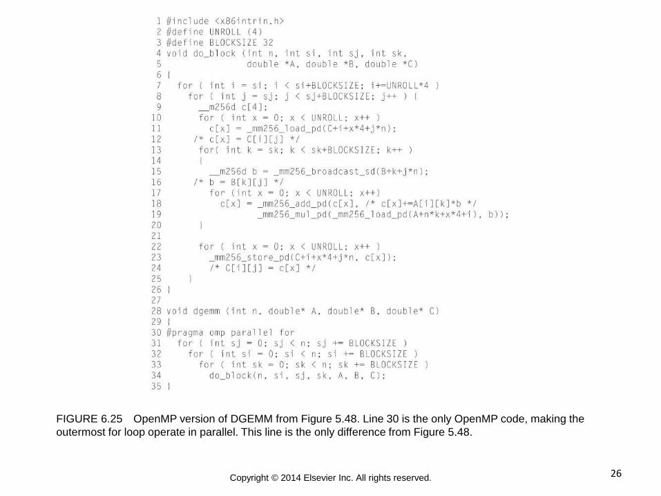
FIGURE 6.25 OpenMP version of DGEMM from Figure 5.48. Line 30 is the only OpenMP code, making the
outermost for loop operate in parallel. This line is the only difference from Figure 5.48.

27 Copyright © 2014 Elsevier Inc. All rights reserved.
FIGURE 6.26 Performance improvements relative to a single thread as the number of threads increase. The
most honest way to present such graphs is to make performance relative to the best version of a single
processor program, which we did. This plot is relative to the performance of the code in Figure 5.48 without
including OpenMP pragmas.
28 Copyright © 2014 Elsevier Inc. All rights reserved.
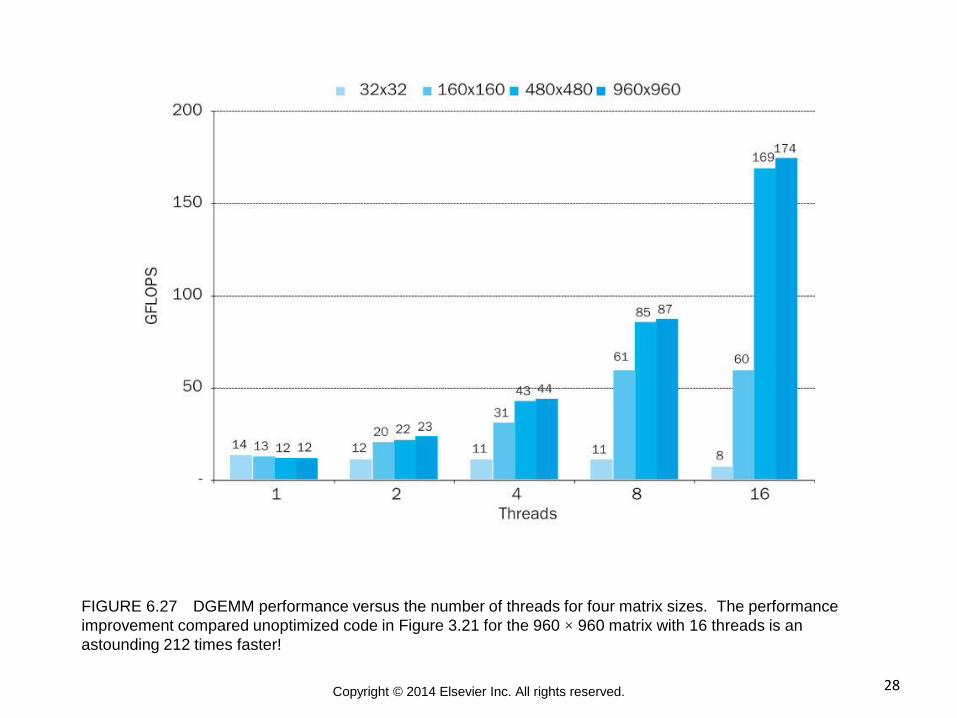
FIGURE 6.27 DGEMM performance versus the number of threads for four matrix sizes. The performance
improvement compared unoptimized code in Figure 3.21 for the 960 × 960 matrix with 16 threads is an
astounding 212 times faster!
29 Copyright © 2014 Elsevier Inc. All rights reserved.
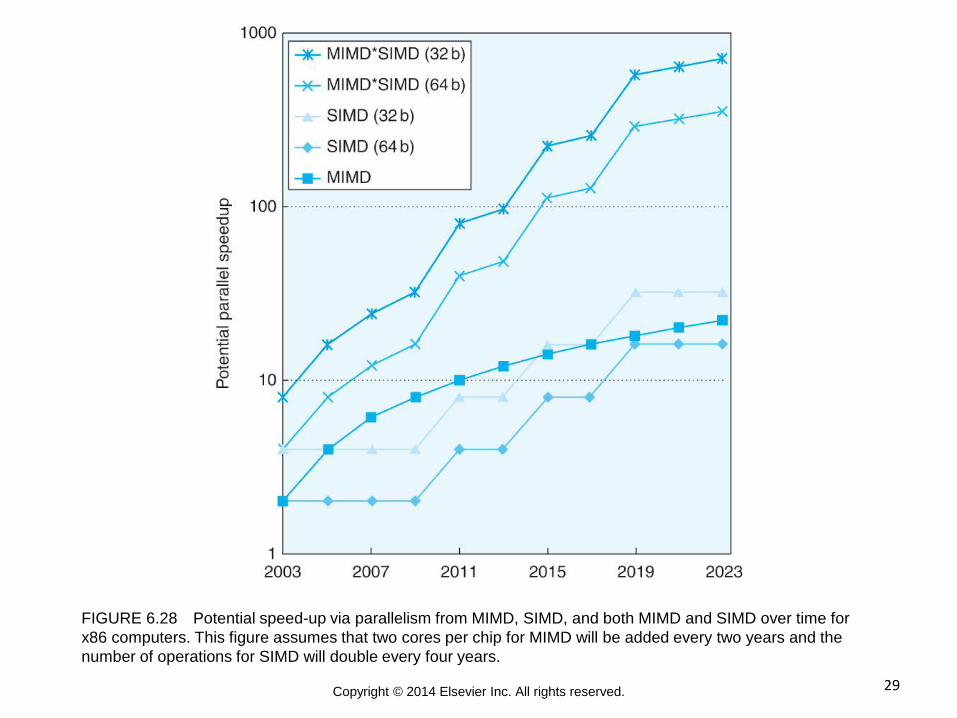
FIGURE 6.28 Potential speed-up via parallelism from MIMD, SIMD, and both MIMD and SIMD over time for
x86 computers. This figure assumes that two cores per chip for MIMD will be added every two years and the
number of operations for SIMD will double every four years.
30 Copyright © 2014 Elsevier Inc. All rights reserved.
Unn Fig. 1

31 Copyright © 2014 Elsevier Inc. All rights reserved.
Unn Fig. 2

32 Copyright © 2014 Elsevier Inc. All rights reserved.
Unn Fig. 3
33 Copyright © 2014 Elsevier Inc. All rights reserved.
Unn Fig. 4

34 Copyright © 2014 Elsevier Inc. All rights reserved.
Unn Fig. 5
35 Copyright © 2014 Elsevier Inc. All rights reserved.
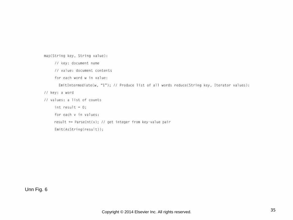
Unn Fig. 6
36 Copyright © 2014 Elsevier Inc. All rights reserved.
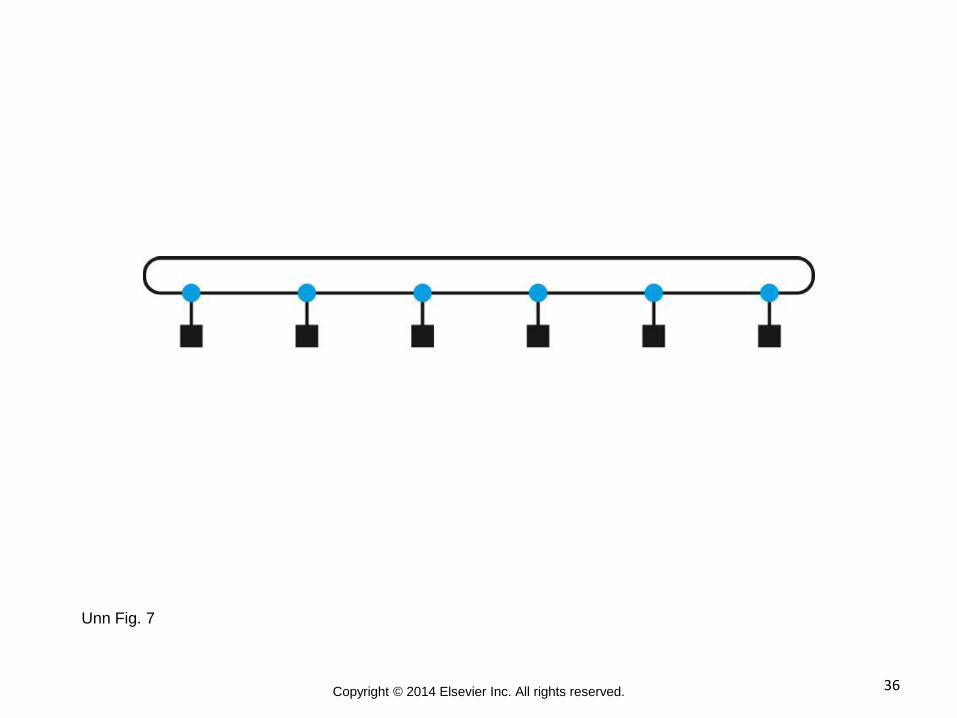
Unn Fig. 7
37 Copyright © 2014 Elsevier Inc. All rights reserved.
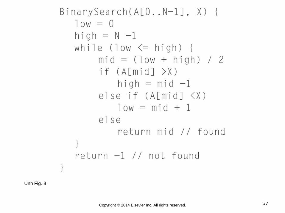
Unn Fig. 8

38 Copyright © 2014 Elsevier Inc. All rights reserved.
Unn Fig. 9
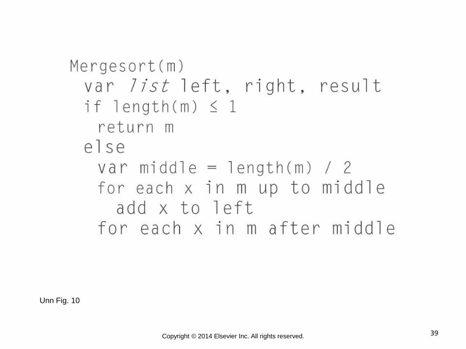
39 Copyright © 2014 Elsevier Inc. All rights reserved.
Unn Fig. 10
40 Copyright © 2014 Elsevier Inc. All rights reserved.
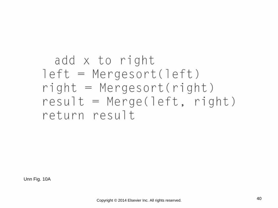
Unn Fig. 10A

41 Copyright © 2014 Elsevier Inc. All rights reserved.
Unn Fig. 11
42 Copyright © 2014 Elsevier Inc. All rights reserved.
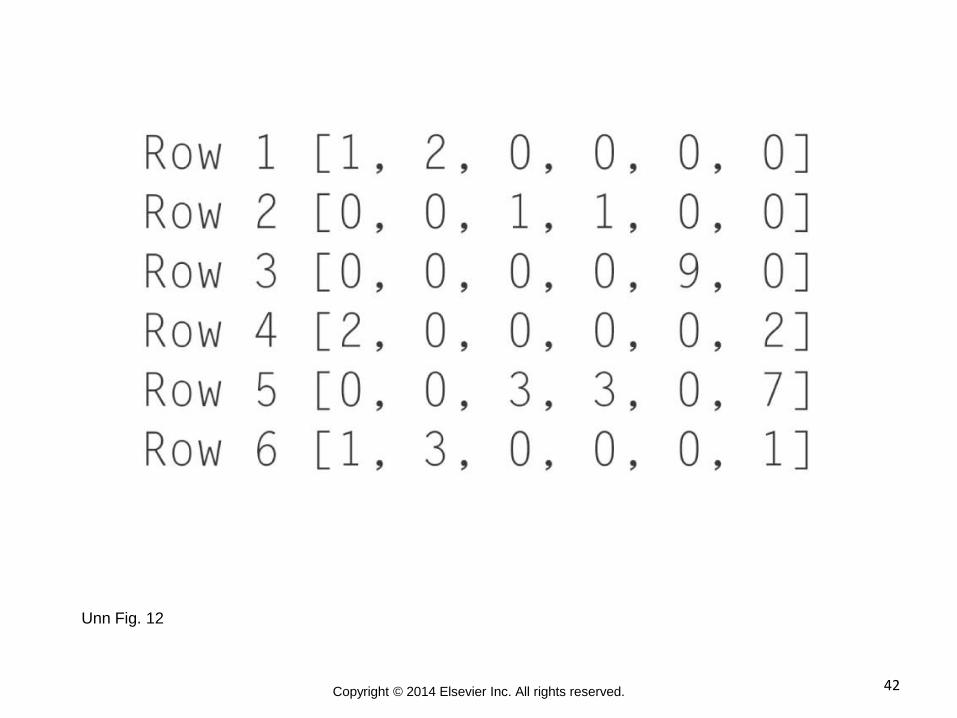
Unn Fig. 12

43 Copyright © 2014 Elsevier Inc. All rights reserved.
Table 1

44 Copyright © 2014 Elsevier Inc. All rights reserved.
Table 2
45 Copyright © 2014 Elsevier Inc. All rights reserved.
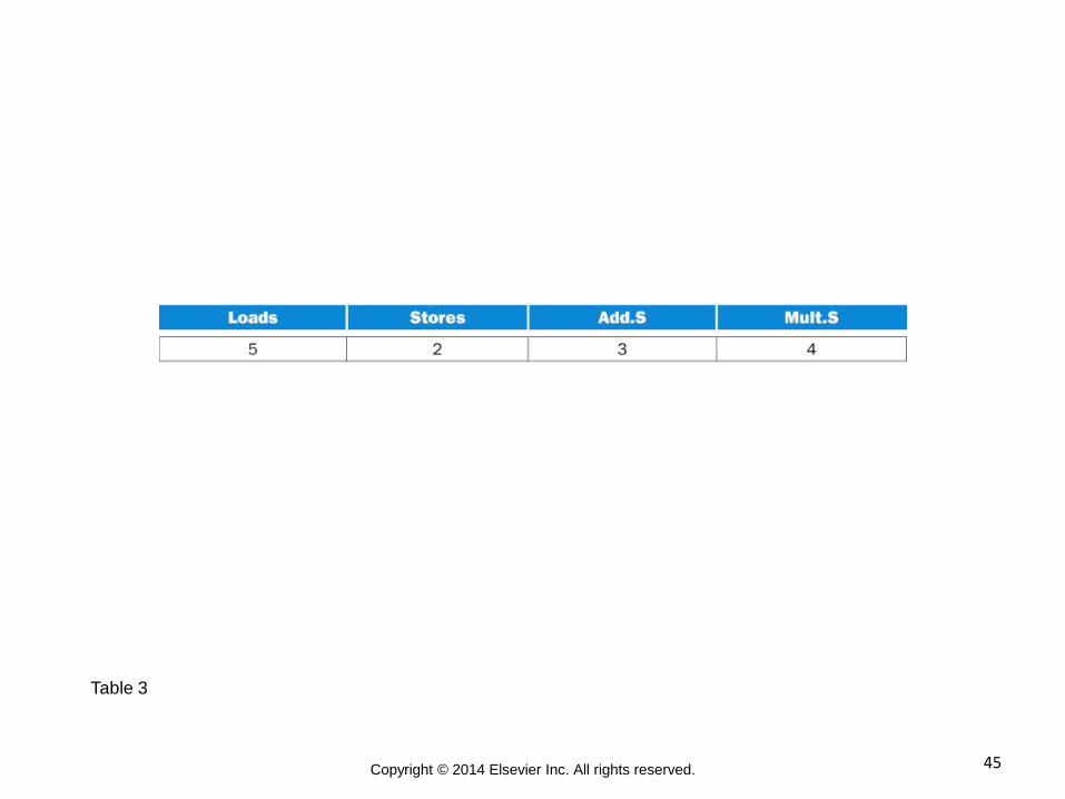
Table 3

46 Copyright © 2014 Elsevier Inc. All rights reserved.
Table 4

47 Copyright © 2014 Elsevier Inc. All rights reserved.
Table 5