chapter 6 hardware prototype...
TRANSCRIPT
107
CHAPTER 6
HARDWARE PROTOTYPE IMPLEMENTATION OF THE
DSTATCOM USING HCC FOR REACTIVE POWER
COMPENSATION
6.1 INTRODUCTION
In today’s scenario, it is very essential to design appropriate
compensators in the power system to improve the power quality. This is due
to the increase in a wide variety of digital loads that pollute the power system.
Improper design of the compensators results in either in its over-capacity or
under-capacity. Over-capacity of the compensators increases the cost of the
system while under-capacity of the compensators leads to an interruption in
the operation of the system. It is necessary to design an appropriate controller
to provide uninterrupted operation at a lower cost by properly selecting the
control system components. This Chapter is devoted for implementing the
hardware prototype of the DSTATCOM for reactive power compensation.
The HCC technique is used to control the prototype DSTATCOM. The
constraints and reasons for using a particular component in the hardware
implementation are also discussed.
The DSTATCOM is controlled in such a way that it exchanges only
reactive power with the grid by injecting current in quadrature with the grid
voltage. As the DSTATCOM is a shunt connected current injecting device,
some simplified assumptions are made to implement the hardware. To
108
compensate for the required amount of reactive power, the DSTATCOM
injects the required current, which is the reference current. If the voltage
source converter (VSC) operates in the closed-loop to supply the reference
current, it is said to supply the specified reactive power to the grid. The
DSTATCOM operates in closed-loop to supply the reference current using the
Hysteresis Current Control (HCC) algorithm. The HCC algorithm is studied
for its performance in MATLAB simulation and digitally implemented in the
prototype hardware using the Xilinx Spartan-3A FPGA controller. The
Spartan-3A kit is programmed using the system generator feature in
MATLAB to convert the MATLAB blocks into the Xilinx code.
6.2 PROBLEM FORMULATION
The DSTATCOM can be viewed as a controlled VSC that operates
in such a way that it supplies the required reference current. HCC is found to
be suitable for the control of the DSTATCOM current; hence, a hardware
controller is designed and tested to achieve this control objective. The
DSTATCOM is tested to supply the required reference current, which is
equivalent to the supply of the required reactive power to the system. The
control law is derived from the instantaneous real power and reactive power
theory. According to this theory, the reference current is computed by
assuming that the real power supply is equal to zero and the reactive power
supply is equal to the load reactive power. The objective is to simulate and
implement the closed loop VSC for validating the concept of reactive power
compensation in the DSTATCOM. This technique also helps in the power
factor improvement. The major problems associated with the implementation
of the DSTATCOM are the selection of the appropriate circuit components
and controllers. It is also required to validate the selection of a particular
components and controllers for the hardware implementation. The other
problem is to understand the proper working of the controller and its
109
algorithms. This problem can be solved by studying the performance of the
system in simulation and then implementing the system in real time.
6.3 OVERVIEW OF THE HARDWARE PROTOTYPE
IMPLEMENTATION
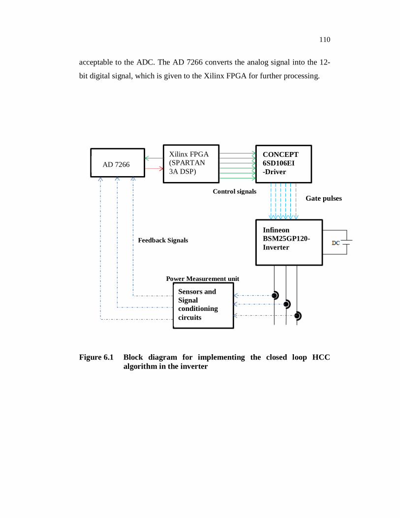
Figure 6.1 shows the basic block diagram for the hardware
implementation of the inverter in the closed-loop HCC technique. The
inverter power module BSM25GP120 is used. The inverter module is tested
by connecting a DC supply at the input side and the three-phase RL load at
the output side. For the DSTATCOM application, the DC supply is replaced
by a DC capacitor on the DC side. The output voltages and currents are
sensed by the voltage sensors LEM-LV25-600P and the current sensors LEM-
LA25NP respectively. The signals from the voltage sensors and the current
sensors are very weak in magnitude and are not suitable for processing them
by the Analog to Digital Converter (ADC) unit of the controller. Hence, it is
essential to use the signal conditioning circuit. The signal conditioning circuit
converts the weak signals from the voltage and current sensors into amplified
signals, which can be fed to the ADC for further processing. The analog to
digital converter, AD 7266, is used for converting the analog signals to the
digital signals that are processed by a suitable controller for implementing the
control algorithms.
The control algorithm is implemented using the Xilinx-SPARTAN
3A FPGA processor. The control signals generated from the FPGA processor
are fed to the driver circuit. The concept scale driver IC 6SD106EI is used as
the driver circuit and provides isolation for the digital controller unit from the
power circuit. The power measurement unit comprises of the voltage sensors,
current sensors and the signal conditioning circuit. This system converts the
power level voltages and currents into low-level voltages and current signals
110
acceptable to the ADC. The AD 7266 converts the analog signal into the 12-
bit digital signal, which is given to the Xilinx FPGA for further processing.
Figure 6.1 Block diagram for implementing the closed loop HCC algorithm in the inverter
Gate pulsesControl signals
Feedback Signals
Power Measurement unit
Sensors and Signalconditioningcircuits
Infineon BSM25GP120-Inverter
CONCEPT6SD106EI -Driver
Xilinx FPGA (SPARTAN 3A DSP)
AD 7266
111
6.4 SELECTION OF THE ANALOG TO DIGITAL
CONVERTERS (ADC)
Due to its low cost and easy availability, the ADC 0808 was chosen
initially for the hardware implementation. It was found to be inefficient for
the DSTATCOM application as its maximum operating clock frequency is
1.2 MHz and the conversion time for each channel is 100 s. For the
DSTATCOM application, at least 8 number of ADC channels are required,
which is available in the ADC 0808. Hence, when using all the 8 channels of
the ADC, the conversion time of all the channels will be 8x100 = 800 s. If a
sine wave signal of 50 Hz is sampled using a channel of ADC 0808, the
number of samples in a cycle is 20 ms / (800 s), which will be 25 samples
per cycle of a sine wave.
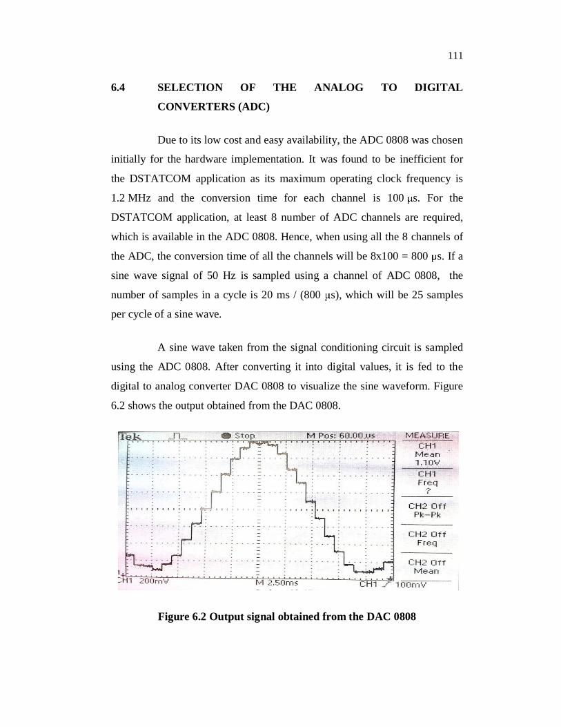
A sine wave taken from the signal conditioning circuit is sampled
using the ADC 0808. After converting it into digital values, it is fed to the
digital to analog converter DAC 0808 to visualize the sine waveform. Figure
6.2 shows the output obtained from the DAC 0808.
Figure 6.2 Output signal obtained from the DAC 0808

112
It is clear from Figure 6.2 that the number of samples taken over a 50 Hz sine
wave is 25, which may lead to large quantization error. The performance of
the ADC is studied through simulation. Figure 6.3 shows the MATLAB
System Generator simulation result of the output load current sampled for
800 s as per the ADC 0808 sample time. It can be inferred from the result
that the load current does not follow the reference load current at this
sampling time. Hence, it is not advisable to use the ADC 0808 for closed-loop
operation.
Figure 6.3 HCC simulation result when the output current is sampled at 800 s
Hence, the AD 7266 is chosen as the ADC to implement the closed-
loop hysteresis current control operation. This ADC is suitable because of the
following features.
1. 12-bit analog to digital conversion (up to 4096 digital
values).
2. The conversion speed can be selected manually with the
SCLK pin.
113
3. The 12-bit digital values are sent serially which reduces the
number of data lines connected to the controller.
4. Two ADC modules are in parallel conversion mode with 6
channels for each ADC module.
The minimum number of ADC channels required to implement the
DSTATCOM is eight. Therefore, four channels in the ADC module A and
four channels in the ADC module B can be selected for optimal performance
and for parallel conversions.
The clock frequency of AD 7266 is 20 MHz
The number of channels used in each module of ADC is 4.
The number of clock cycles required for the serial to parallel
conversion is 10.
The number of clock cycles required for accessing the 12-bit data
from the ADC is 24.
The ADC module conversion time = (No of channel*Total no of
clock cycles) / clock frequency.
When using 4 channels in the ADC module, the conversion time is ×
( × )s and hence the number of samples in a cycle of 50 Hz sine wave is
around 2,941.
The number of samples taken by the AD 7266 (for 4 channels in the
ADC module) is 117 times greater than the number of samples taken by the
ADC 0808. Hence, the AD 7266 is chosen for the DSTATCOM application.
114
6.5 SELECTION OF THE CONTROLLER
In most of the closed loop operation of the inverters, the Digital
Signal Processor (DSP) is used as a controller (Kazmierkowski et al 2011 and
Haibing et al 2012). Even though the DSP has a very high operating speed of
150 MHz, certain observations are made from the initial studies and
experiments on the use of DSP for the DSTATCOM application. Since the
DSP is a sequential architecture device, the control algorithm implemented in
a DSP will be executed sequentially and hence the operation time increases.
To implement the hysteresis current control technique, the current in each
phase of the load must be sensed in parallel. The DSP fails to satisfy this
requirement. When any one phase current is sampled by the ADC channel of
the DSP, the other two phases of the currents will not be sampled. If the ADC
channels available in DSP are multiplexed to a single ADC module as in the
ADC 0808 or the AD 7266, it may lead to the propagation delay problem.
Hence, the results of the hysteresis current control technique may deviate to a
large extent from the simulation results. This can be rectified by using a high-
speed clock for the DSP or by using the PLL technique to speed up the clock
but the reliability of the DSP decreases. Moreover, the architecture of the DSP
cannot be modified to meet our requirements. The number of PWM pins in
the TMS320F2812 is limited and the default dead-band setting by the
manufacturer is discrete, which may not match with the switches in the power
module. The implementation of the digital filter is easy in the DSP kit, but
digital filters are the secondary requirement for this thesis.
The Field Programmable Gated Array (FPGA) has been chosen for
this thesis as it satisfies all the requirements. An FPGA contains hundreds and
millions of logic gates, which can be programmed according to our
requirements. The programming methods of the DSP use a well-defined
architecture for a specific purpose, whereas the programming method of the
115
FPGA requires describing the architecture for a specific purpose. The FPGA
is capable of processing the instructions in parallel, which helps to implement
high-speed algorithms. Hence, to execute highly complex control algorithm at
high-speed, the FPGA is preferable. The HCC technique requires a high
sampling rate to achieve proper control. Since the FPGA channel can be
operated in parallel, the three-phase current signals from the ADC can be
sampled simultaneously. Moreover, the propagation delay of the FPGA is
very small of the order of 1/ , where is the operating speed of the FPGA.
In addition to these features, look-up tables (LUTs) are available in the
FPGA, which is more useful in implementing the vector based hysteresis
current control technique (Sepulveda et al 2013). The implementation of the
digital filters is relatively a complex procedure compared to the DSP. The
speed and parallel operations are the most important requirements than the
use of digital filter in HCC. Hence, the FPGA is chosen as the controller in
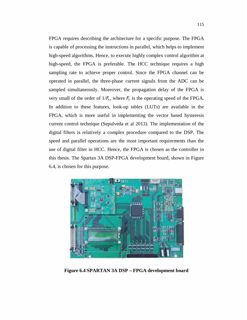
this thesis. The Spartan 3A DSP-FPGA development board, shown in Figure
6.4, is chosen for this purpose.
Figure 6.4 SPARTAN 3A DSP – FPGA development board
116
The important features of the SPARTAN 3A FPGA board are mentioned
below:
1. Xilinx XC3SD1800A – FG676 -4 Spartan 3A DSP FPGA
2. 8 Numbers of digital input using dip switches
3. 16 Numbers of digital outputs using discrete LEDs
4. Reset switch
5. FPGA configuration through
JTAG port
Slave serial
On-board Flash Prom XCF16PV048
6. Total 676 I/O pins available out of which 80 pins used for
integrating peripherals like LED, Switches etc., and the
remaining 110 pins are available for the users.
7. On-board programmable oscillator from 3 MHz to 200 MHz
8. 16 × 2 LCD interface.
The ADC AD 7266 is available with the development board and is
connected through the ADC daughter card interface. The clock setting
jumpers are connected such that the FPGA is operated at 20 MHz speed.
The MATLAB system generator software interface is used to
programme the FPGAs and this reduces the programming time and error.
From the Simulink interface, the VHDL or Verilog code can be generated.
This code can be loaded into the FPGA kit.
117
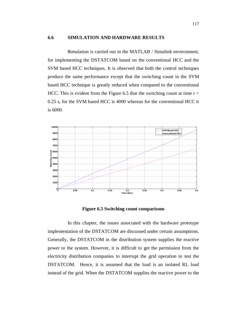
6.6 SIMULATION AND HARDWARE RESULTS
Simulation is carried out in the MATLAB / Simulink environment,
for implementing the DSTATCOM based on the conventional HCC and the
SVM based HCC techniques. It is observed that both the control techniques
produce the same performance except that the switching count in the SVM
based HCC technique is greatly reduced when compared to the conventional
HCC. This is evident from the Figure 6.5 that the switching count at time t =
0.25 s, for the SVM based HCC is 4000 whereas for the conventional HCC it
is 6000.
Figure 6.5 Switching count comparisons
In this chapter, the issues associated with the hardware prototype
implementation of the DSTATCOM are discussed under certain assumptions.
Generally, the DSTATCOM in the distribution system supplies the reactive
power to the system. However, it is difficult to get the permission from the
electricity distribution companies to interrupt the grid operation to test the
DSTATCOM. Hence, it is assumed that the load is an isolated RL load
instead of the grid. When the DSTATCOM supplies the reactive power to the
0 0.05 0.1 0.15 0.2 0.25 0.3 0.35 0.40
1000
2000
3000
4000
5000
6000
7000
8000
9000
10000
Time (Sec)
SVM Based HCCConventional HCC
118
grid, it injects the current in quadrature with the grid voltage. Hence, the
DSTATCOM is tested to supply required current to the isolated load. The
HCC technique is used to supply the required reference current to the load,
which implies the supply of required reactive power to the load. The reference
current obtained in simulation is compared with the output current obtained
from the hardware prototype model. Table 6.1 shows the simulation
parameters in the MATLAB simulation model.
Table 6.1 Simulation parameters of the distribution system with DSTATCOM
Parameters Values
Base Voltage (V) 400
Base kVA (kVA) 4
Line Resistance ( /km) 0.2
Line Reactance ( /km) 0.0314
Total Line Length (km) 10
VSI Filter Inductance (mH) 10
Load A ( ) 5 + j7.85
Load B ( ) 10 + j3.14
Capacitor Value ( F) 330
6.7 HARDWARE RESULTS
The prototype inverter module is fabricated using the
BSM25GP120 power module as discussed. Initially, in order to ensure the
proper working of the inverter module, a driver module and a controller unit,
the SVPWM switching technique is implemented with a 0.5 HP 3-phase
induction motor load in open-loop and the load current results are obtained.
Figure 6.7 shows the load current supplied by the SVPWM based inverter,
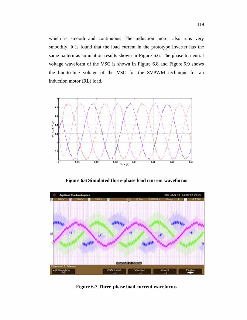
119
which is smooth and continuous. The induction motor also runs very
smoothly. It is found that the load current in the prototype inverter has the
same pattern as simulation results shown in Figure 6.6. The phase to neutral
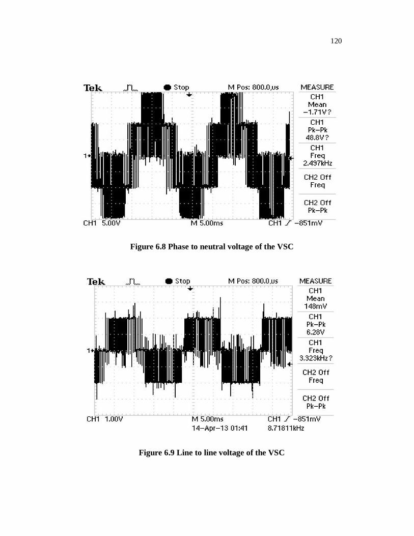
voltage waveform of the VSC is shown in Figure 6.8 and Figure 6.9 shows
the line-to-line voltage of the VSC for the SVPWM technique for an
induction motor (RL) load.
Figure 6.6 Simulated three-phase load current waveforms
Figure 6.7 Three-phase load current waveforms
0 0.01 0.02 0.03 0.04 0.05 0.06 0.07
0.8
1
1.2
1.4
1.6
1.8
2
Time (S)
120
Figure 6.8 Phase to neutral voltage of the VSC
Figure 6.9 Line to line voltage of the VSC
121
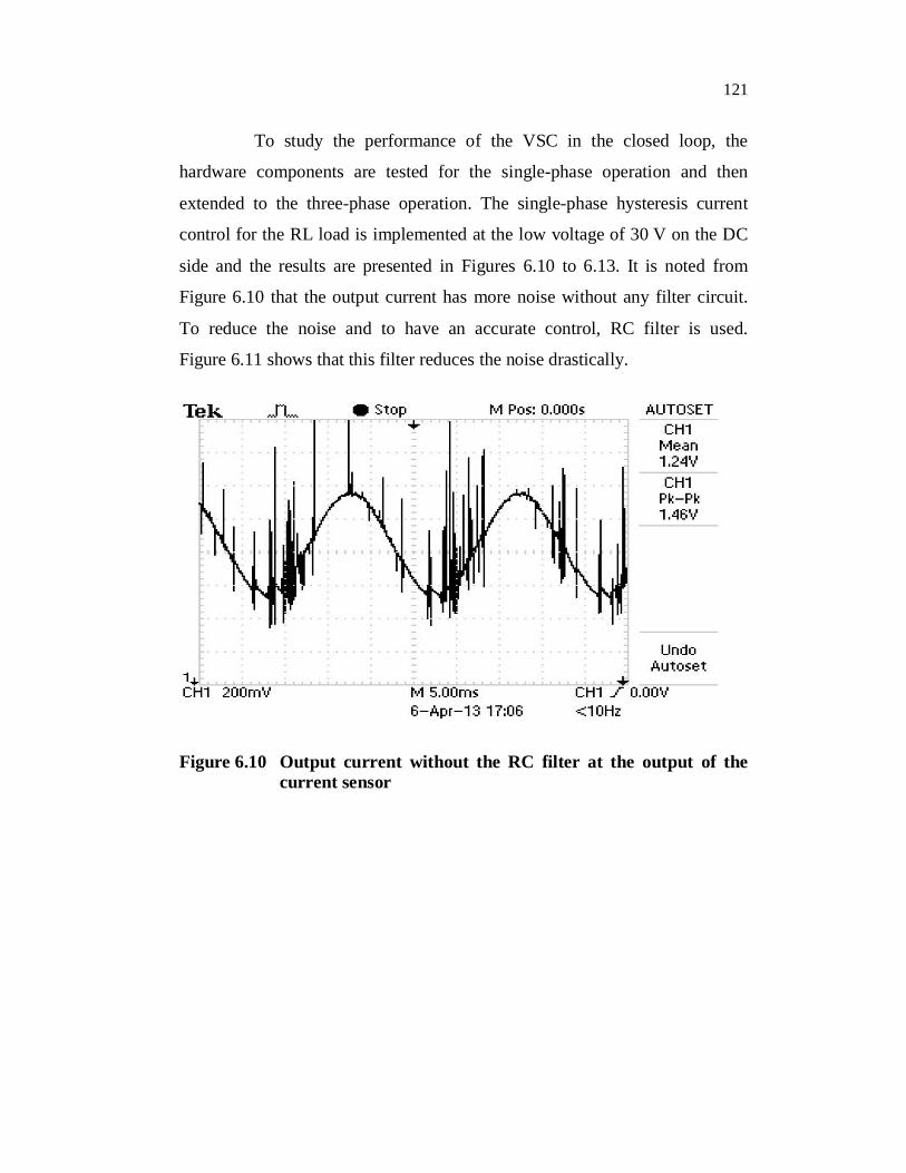
To study the performance of the VSC in the closed loop, the
hardware components are tested for the single-phase operation and then
extended to the three-phase operation. The single-phase hysteresis current
control for the RL load is implemented at the low voltage of 30 V on the DC
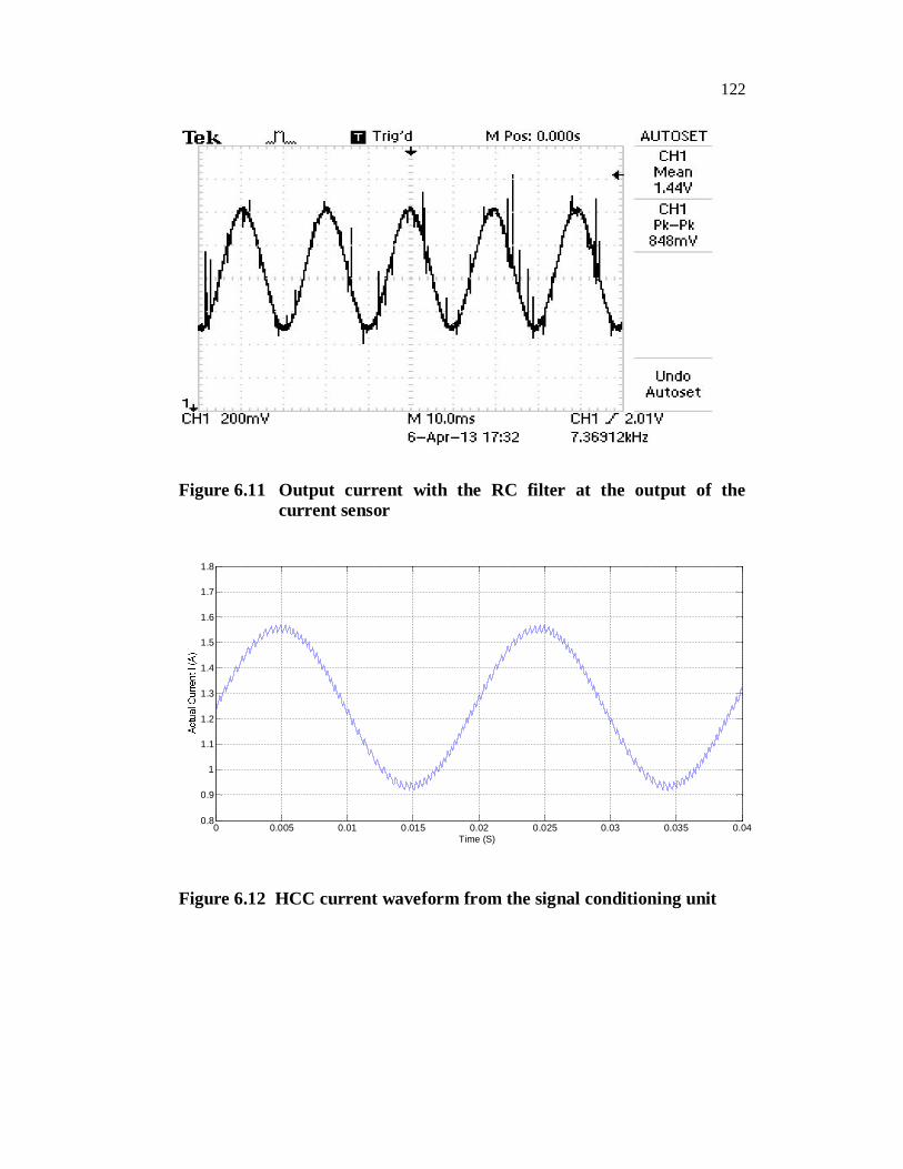
side and the results are presented in Figures 6.10 to 6.13. It is noted from
Figure 6.10 that the output current has more noise without any filter circuit.
To reduce the noise and to have an accurate control, RC filter is used.
Figure 6.11 shows that this filter reduces the noise drastically.
Figure 6.10 Output current without the RC filter at the output of the current sensor
122
Figure 6.11 Output current with the RC filter at the output of the current sensor
Figure 6.12 HCC current waveform from the signal conditioning unit
0 0.005 0.01 0.015 0.02 0.025 0.03 0.035 0.040.8
0.9
1
1.1
1.2
1.3
1.4
1.5
1.6
1.7
1.8
Time (S)
123
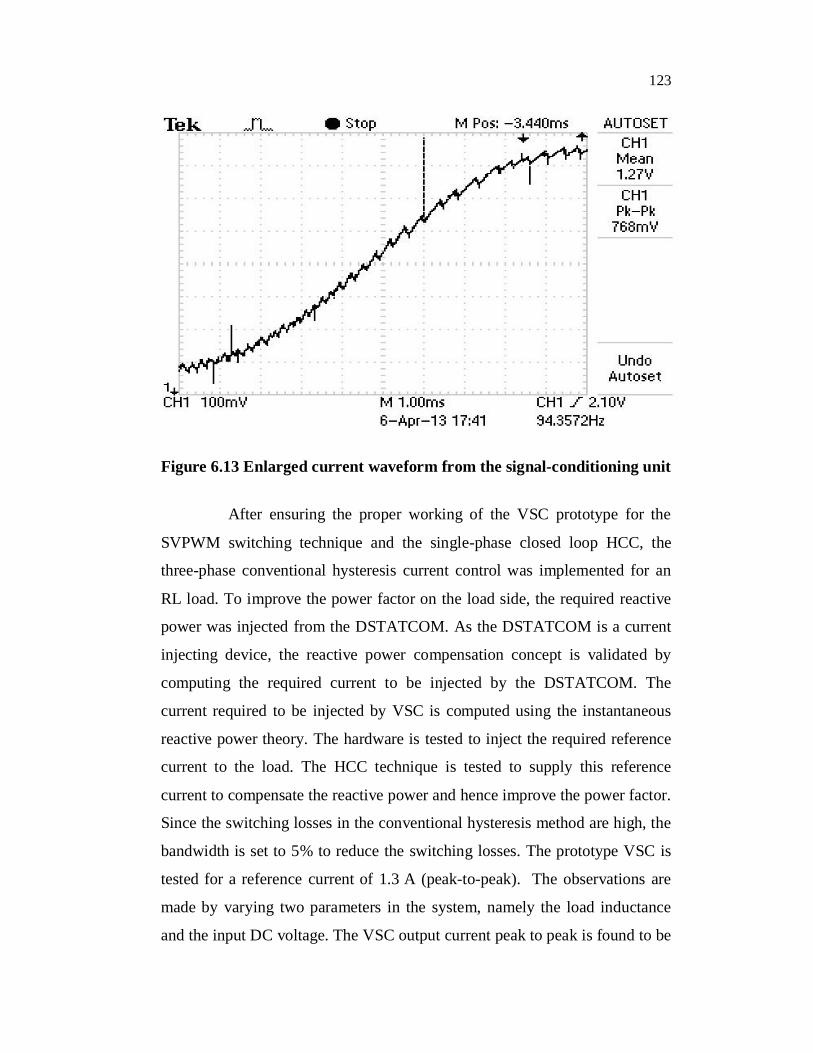
Figure 6.13 Enlarged current waveform from the signal-conditioning unit
After ensuring the proper working of the VSC prototype for the
SVPWM switching technique and the single-phase closed loop HCC, the
three-phase conventional hysteresis current control was implemented for an
RL load. To improve the power factor on the load side, the required reactive
power was injected from the DSTATCOM. As the DSTATCOM is a current
injecting device, the reactive power compensation concept is validated by
computing the required current to be injected by the DSTATCOM. The
current required to be injected by VSC is computed using the instantaneous
reactive power theory. The hardware is tested to inject the required reference
current to the load. The HCC technique is tested to supply this reference
current to compensate the reactive power and hence improve the power factor.
Since the switching losses in the conventional hysteresis method are high, the
bandwidth is set to 5% to reduce the switching losses. The prototype VSC is
tested for a reference current of 1.3 A (peak-to-peak). The observations are
made by varying two parameters in the system, namely the load inductance
and the input DC voltage. The VSC output current peak to peak is found to be
124
constant for the change in the load or the input voltage. The actual current
follows the reference current. Thus, the control objective is achieved. Hence,
the proper working of the three-phase conventional HCC method is validated.
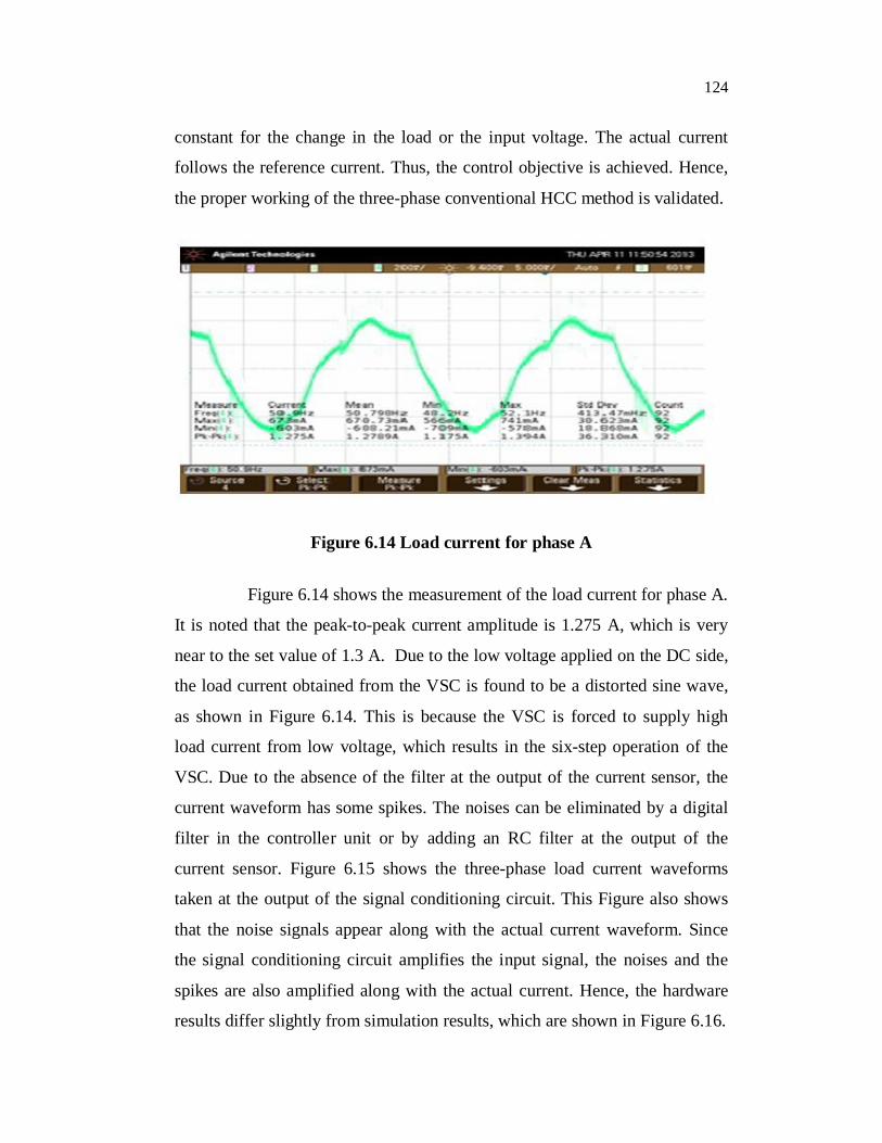
Figure 6.14 Load current for phase A
Figure 6.14 shows the measurement of the load current for phase A.
It is noted that the peak-to-peak current amplitude is 1.275 A, which is very
near to the set value of 1.3 A. Due to the low voltage applied on the DC side,
the load current obtained from the VSC is found to be a distorted sine wave,
as shown in Figure 6.14. This is because the VSC is forced to supply high
load current from low voltage, which results in the six-step operation of the
VSC. Due to the absence of the filter at the output of the current sensor, the
current waveform has some spikes. The noises can be eliminated by a digital
filter in the controller unit or by adding an RC filter at the output of the
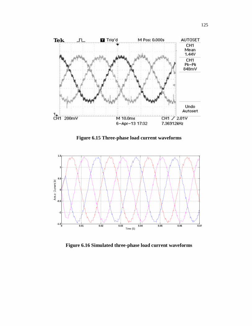
current sensor. Figure 6.15 shows the three-phase load current waveforms
taken at the output of the signal conditioning circuit. This Figure also shows
that the noise signals appear along with the actual current waveform. Since
the signal conditioning circuit amplifies the input signal, the noises and the
spikes are also amplified along with the actual current. Hence, the hardware
results differ slightly from simulation results, which are shown in Figure 6.16.
125
Figure 6.15 Three-phase load current waveforms
Figure 6.16 Simulated three-phase load current waveforms
0 0.01 0.02 0.03 0.04 0.05 0.06 0.07-1.5
-1
-0.5
0
0.5
1
1.5
Time (S)
126
Figure 6.17 Actual load current through the signal conditioning circuit
Figure 6.18 Zoomed portion of the actual load current through signal conditioning circuit
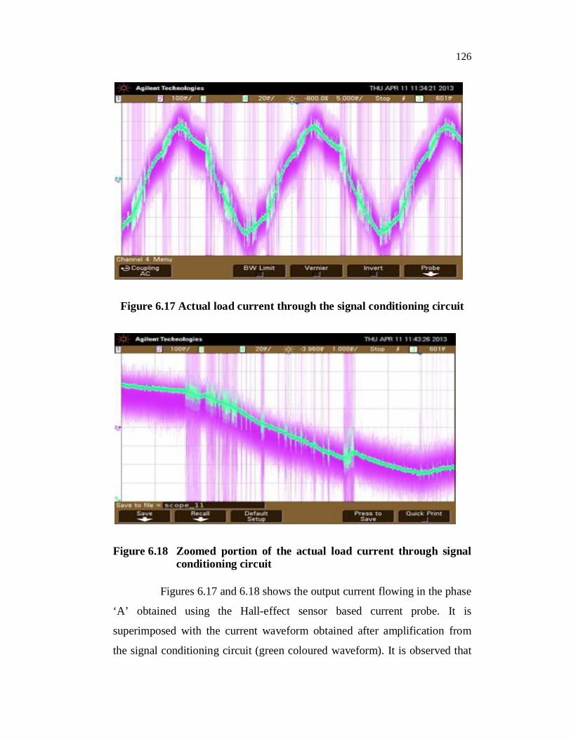
Figures 6.17 and 6.18 shows the output current flowing in the phase
‘A’ obtained using the Hall-effect sensor based current probe. It is
superimposed with the current waveform obtained after amplification from
the signal conditioning circuit (green coloured waveform). It is observed that
127
unnecessary spikes are amplified by the signal conditioning circuit, which is
fed to the ADC of the controller. Hence, it is necessary to implement a filter
before feeding the signal conditioning output to the ADC for the proper
operation of the controller.
6.8 HARDWARE PROTOTYPE IMPLEMENTATION DETAILS
The inverter module, the driver module and the signal
conditioning circuit have been fabricated in the PCB using
Eagle Cad Soft software.
All simulations have been carried out using MATLAB. The
HCC algorithm has been implemented using two basic
approaches.
1. The conventional HCC
2. The SV based HCC
A closed loop control system has been implemented on the
FPGA using the Xilinx software. The MATLAB SysGen
software aids in programming the FPGA kit.
The power supply requirements and triggering the voltage
level of the inverter switches have been determined.
The voltage sensors LEM-LV25-600 and current sensors
LEM-LA25NP are used in the measurement circuit of the
DSTATCOM hardware prototype implementation. In this
thesis, three voltage sensors and five current sensors are used
and all the sensors are calibrated.
128
6.9 HARDWARE IMPLEMENTATION OF THE SIGNAL
CONDITIONING CIRCUIT
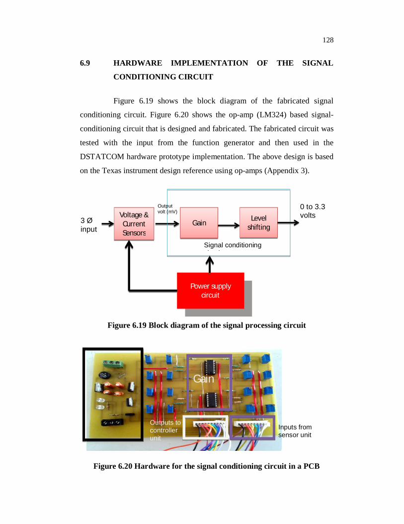
Figure 6.19 shows the block diagram of the fabricated signal
conditioning circuit. Figure 6.20 shows the op-amp (LM324) based signal-
conditioning circuit that is designed and fabricated. The fabricated circuit was
tested with the input from the function generator and then used in the
DSTATCOM hardware prototype implementation. The above design is based
on the Texas instrument design reference using op-amps (Appendix 3).
Figure 6.19 Block diagram of the signal processing circuit
Figure 6.20 Hardware for the signal conditioning circuit in a PCB
OP-AMPs
Power supply circuit
Inputs from sensor unit
Outputs to controller unit
Gain
0 to 3.3 voltsVoltage &
Current Sensors
Gain Level
shifting 3 Ø input
Output volt (mV)
Power supply circuit
Signal conditioning circuit
129
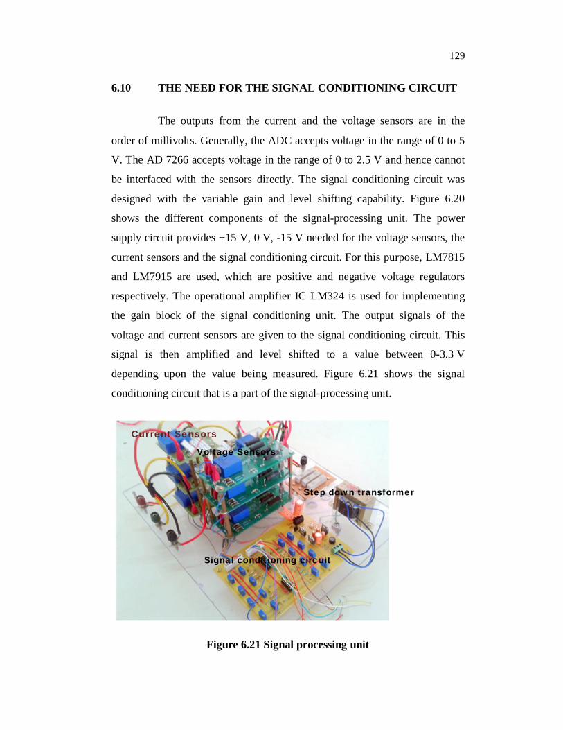
6.10 THE NEED FOR THE SIGNAL CONDITIONING CIRCUIT
The outputs from the current and the voltage sensors are in the
order of millivolts. Generally, the ADC accepts voltage in the range of 0 to 5
V. The AD 7266 accepts voltage in the range of 0 to 2.5 V and hence cannot
be interfaced with the sensors directly. The signal conditioning circuit was
designed with the variable gain and level shifting capability. Figure 6.20
shows the different components of the signal-processing unit. The power
supply circuit provides +15 V, 0 V, -15 V needed for the voltage sensors, the
current sensors and the signal conditioning circuit. For this purpose, LM7815
and LM7915 are used, which are positive and negative voltage regulators
respectively. The operational amplifier IC LM324 is used for implementing
the gain block of the signal conditioning unit. The output signals of the
voltage and current sensors are given to the signal conditioning circuit. This
signal is then amplified and level shifted to a value between 0-3.3 V
depending upon the value being measured. Figure 6.21 shows the signal
conditioning circuit that is a part of the signal-processing unit.
Figure 6.21 Signal processing unit
Current Sensors
Voltage Sensors
Signal conditioning circuit
Step down transformer
130
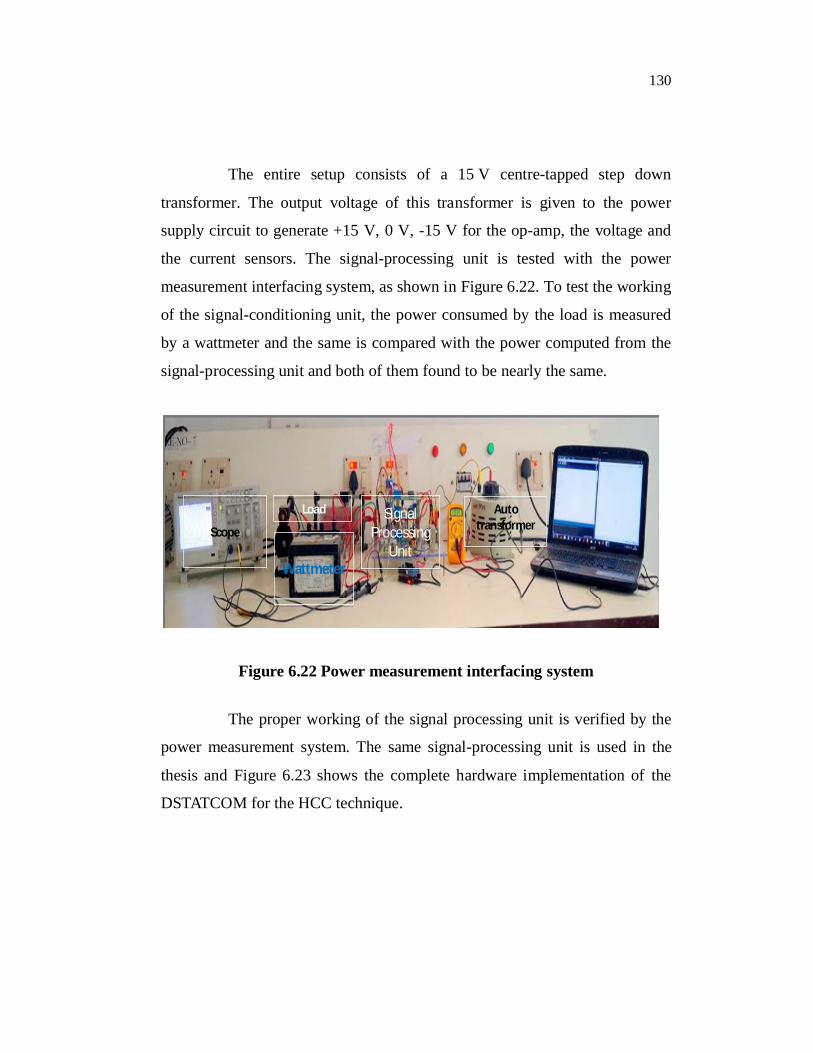
The entire setup consists of a 15 V centre-tapped step down
transformer. The output voltage of this transformer is given to the power
supply circuit to generate +15 V, 0 V, -15 V for the op-amp, the voltage and
the current sensors. The signal-processing unit is tested with the power
measurement interfacing system, as shown in Figure 6.22. To test the working
of the signal-conditioning unit, the power consumed by the load is measured
by a wattmeter and the same is compared with the power computed from the
signal-processing unit and both of them found to be nearly the same.
Figure 6.22 Power measurement interfacing system
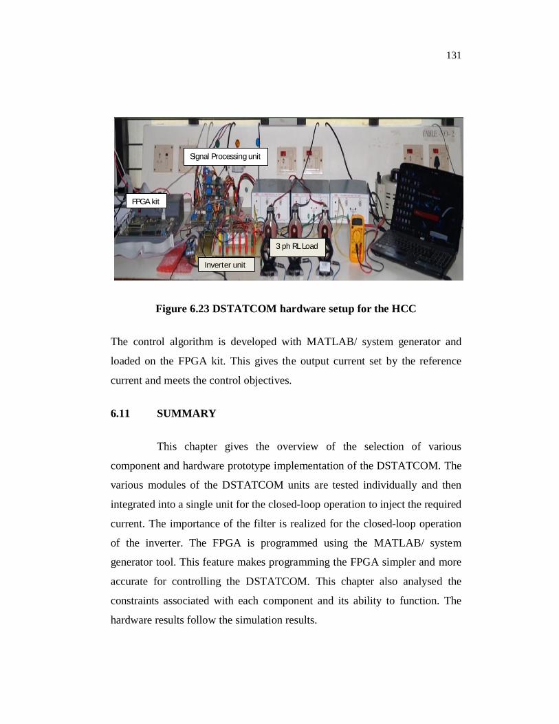
The proper working of the signal processing unit is verified by the
power measurement system. The same signal-processing unit is used in the
thesis and Figure 6.23 shows the complete hardware implementation of the
DSTATCOM for the HCC technique.
Signal Processing
UnitWattmeter
Load Auto transformerScope
131
Figure 6.23 DSTATCOM hardware setup for the HCC
The control algorithm is developed with MATLAB/ system generator and
loaded on the FPGA kit. This gives the output current set by the reference
current and meets the control objectives.
6.11 SUMMARY
This chapter gives the overview of the selection of various
component and hardware prototype implementation of the DSTATCOM. The
various modules of the DSTATCOM units are tested individually and then
integrated into a single unit for the closed-loop operation to inject the required
current. The importance of the filter is realized for the closed-loop operation
of the inverter. The FPGA is programmed using the MATLAB/ system
generator tool. This feature makes programming the FPGA simpler and more
accurate for controlling the DSTATCOM. This chapter also analysed the
constraints associated with each component and its ability to function. The
hardware results follow the simulation results.
FPGA kit
Inverter unit
Signal Processing unit
3 ph RL Load