chapter 7: islamic university of gazasite.iugaza.edu.ps/tskaik/files/chapter7.pdf · electronic...
TRANSCRIPT

Chapter 7:
FET Biasing
Islamic University of Gaza
Dr. Talal Skaik

Copyright ©2009 by Pearson Education, Inc.
Upper Saddle River, New Jersey 07458 • All rights reserved.
Electronic Devices and Circuit Theory, 10/e Robert L. Boylestad and Louis Nashelsky
Basic Current Relationships
For all FETs:
A0IG
SD II
For JFETS and D-Type MOSFETs:
2
P
GSDSSD
V
V1II
For E-Type MOSFETs:
2TGSD )VV(kI
2 Dr. Talal Skaik 2014

Copyright ©2009 by Pearson Education, Inc.
Upper Saddle River, New Jersey 07458 • All rights reserved.
Electronic Devices and Circuit Theory, 10/e Robert L. Boylestad and Louis Nashelsky
2
0
0, ,
1
G
DS DD D D
S D DS GS GG
GSD DSS
p
I A
V V I R
V V V V V
VI I
V
Fixed-Bias Configuration
3 Dr. Talal Skaik 2014
Network for dc analysis.

Copyright ©2009 by Pearson Education, Inc.
Upper Saddle River, New Jersey 07458 • All rights reserved.
Electronic Devices and Circuit Theory, 10/e Robert L. Boylestad and Louis Nashelsky
Fixed-Bias Configuration –Graphical Solution
4 Dr. Talal Skaik 2014
Plotting Shockley’s equation. Finding the solution for the
fixed-bias configuration.
2
1 GSD DSS
p
VI I
V
Copyright ©2009 by Pearson Education, Inc.
Upper Saddle River, New Jersey 07458 • All rights reserved.
Electronic Devices and Circuit Theory, 10/e Robert L. Boylestad and Louis Nashelsky
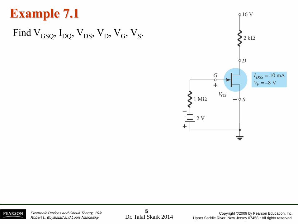
Example 7.1
5 Dr. Talal Skaik 2014
Find VGSQ, IDQ, VDS, VD, VG, VS.

Copyright ©2009 by Pearson Education, Inc.
Upper Saddle River, New Jersey 07458 • All rights reserved.
Electronic Devices and Circuit Theory, 10/e Robert L. Boylestad and Louis Nashelsky
Example 7.1 - graphical solution
6 Dr. Talal Skaik 2014

Copyright ©2009 by Pearson Education, Inc.
Upper Saddle River, New Jersey 07458 • All rights reserved.
Electronic Devices and Circuit Theory, 10/e Robert L. Boylestad and Louis Nashelsky
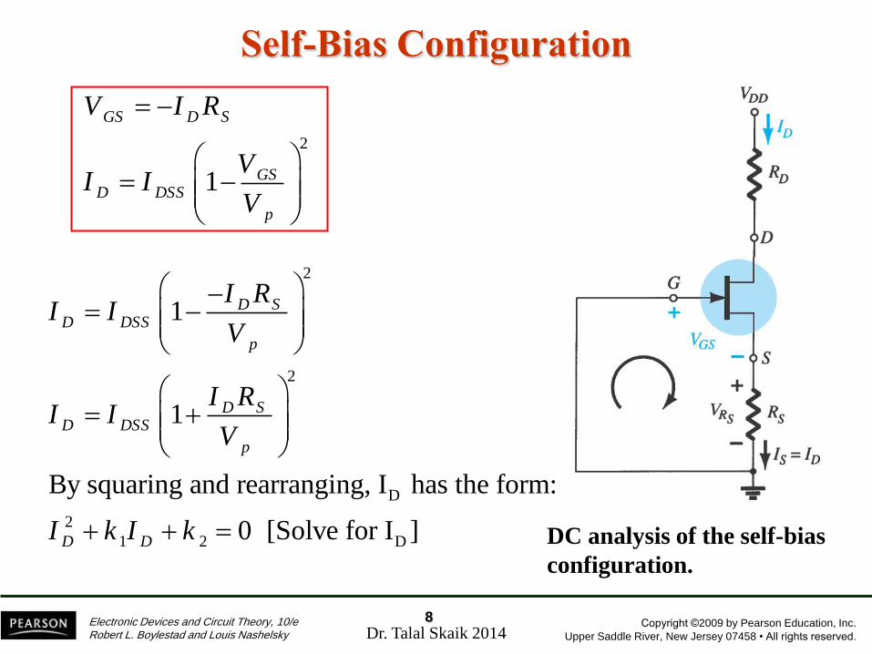
Self-Bias Configuration
7 Dr. Talal Skaik 2014
DC analysis of the self-bias
configuration.
Copyright ©2009 by Pearson Education, Inc.
Upper Saddle River, New Jersey 07458 • All rights reserved.
Electronic Devices and Circuit Theory, 10/e Robert L. Boylestad and Louis Nashelsky
Self-Bias Configuration
8 Dr. Talal Skaik 2014
DC analysis of the self-bias
configuration.
2
1
GS D S
GSD DSS
p
V I R
VI I
V
2
2
D
2
1 2 D
1
1
By squaring and rearranging, I has the form:
0 [Solve for I ]
D SD DSS
p
D SD DSS
p
D D
I RI I
V
I RI I
V
I k I k
Copyright ©2009 by Pearson Education, Inc.
Upper Saddle River, New Jersey 07458 • All rights reserved.
Electronic Devices and Circuit Theory, 10/e Robert L. Boylestad and Louis Nashelsky
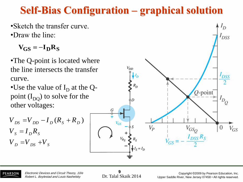
Self-Bias Configuration – graphical solution
9 Dr. Talal Skaik 2014
SDGS RIV
•Sketch the transfer curve.
•Draw the line:
•The Q-point is located where
the line intersects the transfer
curve.
•Use the value of ID at the Q-
point (IDQ) to solve for the
other voltages:
( )DS DD D S D
S D S
D DS S
V V I R R
V I R
V V V

Copyright ©2009 by Pearson Education, Inc.
Upper Saddle River, New Jersey 07458 • All rights reserved.
Electronic Devices and Circuit Theory, 10/e Robert L. Boylestad and Louis Nashelsky
Example 7.2
10 Dr. Talal Skaik 2014
Find VGSQ, IDQ, VDS, VD, VG, VS.
Solution
Draw the line: SDGS RIV

Copyright ©2009 by Pearson Education, Inc.
Upper Saddle River, New Jersey 07458 • All rights reserved.
Electronic Devices and Circuit Theory, 10/e Robert L. Boylestad and Louis Nashelsky
Example 7.2 - solution
11 Dr. Talal Skaik 2014
Determining the Q-point
for the network.
Sketching the device
characteristics for the JFET

Copyright ©2009 by Pearson Education, Inc.
Upper Saddle River, New Jersey 07458 • All rights reserved.
Electronic Devices and Circuit Theory, 10/e Robert L. Boylestad and Louis Nashelsky
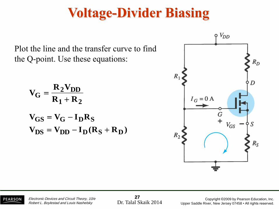
Voltage-Divider Bias
IG = 0 A
IR1=IR2
12 Dr. Talal Skaik 2014
Redrawn network for dc analysis.

Copyright ©2009 by Pearson Education, Inc.
Upper Saddle River, New Jersey 07458 • All rights reserved.
Electronic Devices and Circuit Theory, 10/e Robert L. Boylestad and Louis Nashelsky
Voltage-Divider Bias
13 Dr. Talal Skaik 2014
The Q point is established by
plotting a line that intersects the
transfer curve.
21
DD2G
RR
VRV
VG is equal to the voltage across
divider resistor R2:
Using Kirchhoff’s Law:
SDGGS RIVV

Copyright ©2009 by Pearson Education, Inc.
Upper Saddle River, New Jersey 07458 • All rights reserved.
Electronic Devices and Circuit Theory, 10/e Robert L. Boylestad and Louis Nashelsky
Voltage-Divider Bias
14 Dr. Talal Skaik 2014
Step 1
Plot the line by plotting two
points:
•VGS = VG, ID = 0 A
•VGS = 0 V, ID = VG / RS
Step 2
Plot the transfer curve by plotting
IDSS, VP and the calculated values
of ID
Step 3
The Q-point is located where the
line intersects the transfer curve
SDGGS RIVV

Copyright ©2009 by Pearson Education, Inc.
Upper Saddle River, New Jersey 07458 • All rights reserved.
Electronic Devices and Circuit Theory, 10/e Robert L. Boylestad and Louis Nashelsky
Voltage-Divider Bias
15 Dr. Talal Skaik 2014
SDGGS RIVV
Effect of RS on the resulting Q-point.

Copyright ©2009 by Pearson Education, Inc.
Upper Saddle River, New Jersey 07458 • All rights reserved.
Electronic Devices and Circuit Theory, 10/e Robert L. Boylestad and Louis Nashelsky
Voltage-Divider Bias
16 Dr. Talal Skaik 2014
Using the value of ID at the Q-point, solve for the other variables in
the voltage-divider bias circuit:
SDS
DDDDD
SDDDDDS
RIV
RIVV
)R(RIVV
21
DDR2R1
RR
VII

Copyright ©2009 by Pearson Education, Inc.
Upper Saddle River, New Jersey 07458 • All rights reserved.
Electronic Devices and Circuit Theory, 10/e Robert L. Boylestad and Louis Nashelsky
Example 7.5
17 Dr. Talal Skaik 2014
Find VGSQ, IDQ, VDS, VD, VG, VS.

Copyright ©2009 by Pearson Education, Inc.
Upper Saddle River, New Jersey 07458 • All rights reserved.
Electronic Devices and Circuit Theory, 10/e Robert L. Boylestad and Louis Nashelsky
D-Type MOSFET Bias Circuits
Depletion-type MOSFET
bias circuits are similar to
those used to bias JFETs.
The only difference is that
depletion-type MOSFETs
can operate with positive
values of VGS and with ID
values that exceed IDSS.
18 Dr. Talal Skaik 2014

Copyright ©2009 by Pearson Education, Inc.
Upper Saddle River, New Jersey 07458 • All rights reserved.
Electronic Devices and Circuit Theory, 10/e Robert L. Boylestad and Louis Nashelsky
Example 7.7
19 Dr. Talal Skaik 2014
SDGGS RIVV
Step 1 Plot the line for
•VGS = VG, ID = 0 A
•ID = VG/RS, VGS = 0 V
Step 2 Plot the transfer curve using IDSS, VP and
calculated values of ID.
Step 3 The Q-point is located where the line
intersects the transfer curve is. Use the ID at
the Q-point to solve for the other variables in
the voltage-divider bias circuit.
These are the same steps used to
analyze JFET voltage-divider bias
circuits.
21
DD2G
RR
VRV
Find VGSQ, IDQ, VDS
Copyright ©2009 by Pearson Education, Inc.
Upper Saddle River, New Jersey 07458 • All rights reserved.
Electronic Devices and Circuit Theory, 10/e Robert L. Boylestad and Louis Nashelsky
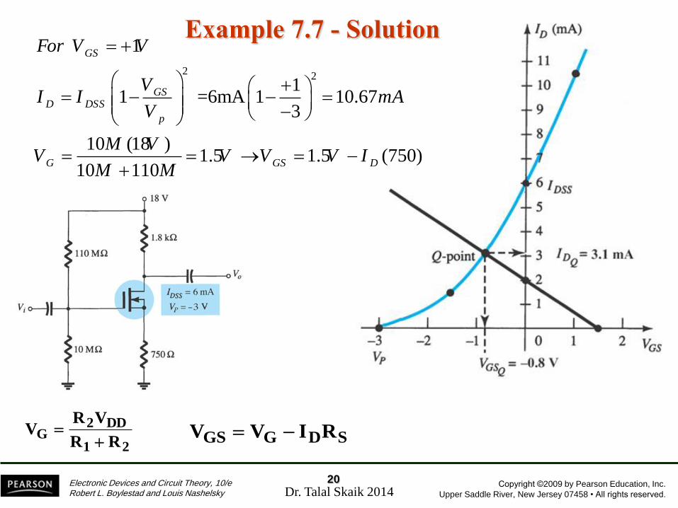
Example 7.7 - Solution
20 Dr. Talal Skaik 2014
SDGGS RIVV 21
DD2G
RR
VRV
22
1
11 =6mA 1 10.67
3
10 (18 )1.5 1.5 (750)
10 110
GS
GSD DSS
p
G GS D
For V V
VI I mA
V
M VV V V V I
M M
Copyright ©2009 by Pearson Education, Inc.
Upper Saddle River, New Jersey 07458 • All rights reserved.
Electronic Devices and Circuit Theory, 10/e Robert L. Boylestad and Louis Nashelsky
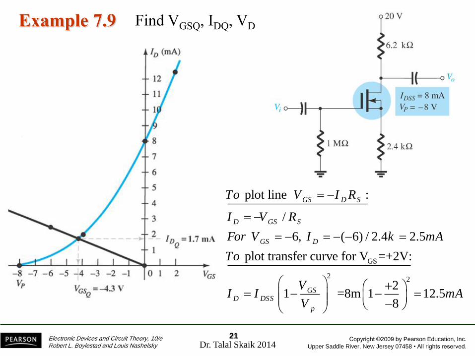
Example 7.9
21 Dr. Talal Skaik 2014
Find VGSQ, IDQ, VD
GS
22
plot line :
/
6, ( 6) / 2.4 2.5
plot transfer curve for V =+2V:
21 =8m 1 12.5
8
GS D S
D GS S
GS D
GSD DSS
p
To V I R
I V R
For V I k mA
To
VI I mA
V

Copyright ©2009 by Pearson Education, Inc.
Upper Saddle River, New Jersey 07458 • All rights reserved.
Electronic Devices and Circuit Theory, 10/e Robert L. Boylestad and Louis Nashelsky
E-Type MOSFET Bias Circuits
The transfer characteristic for
the e-type MOSFET is very
different from that of a simple
JFET or the d-type MOSFET.
22 Dr. Talal Skaik 2014
2
( )D GS GS ThI k V V

Copyright ©2009 by Pearson Education, Inc.
Upper Saddle River, New Jersey 07458 • All rights reserved.
Electronic Devices and Circuit Theory, 10/e Robert L. Boylestad and Louis Nashelsky
Feedback Bias Circuit
IG = 0 A
VRG = 0 V
VDS = VGS
VGS = VDD – IDRD
23 Dr. Talal Skaik 2014
DC equivalent of the network

Copyright ©2009 by Pearson Education, Inc.
Upper Saddle River, New Jersey 07458 • All rights reserved.
Electronic Devices and Circuit Theory, 10/e Robert L. Boylestad and Louis Nashelsky
Feedback Bias Q-Point Step 1
Plot the line using
•VGS = VDD, ID = 0 A
•ID = VDD / RD , VGS = 0 V
Step 2
Using values from the specification
sheet, plot the transfer curve with
•VGSTh , ID = 0 A
•VGS(on), ID(on)
Step 3
The Q-point is located where the
line and the transfer curve intersect
Step 4
Using the value of ID at the Q-
point, solve for the other variables
in the bias circuit.
24 Dr. Talal Skaik 2014
VGS = VDD – IDRD
Copyright ©2009 by Pearson Education, Inc.
Upper Saddle River, New Jersey 07458 • All rights reserved.
Electronic Devices and Circuit Theory, 10/e Robert L. Boylestad and Louis Nashelsky
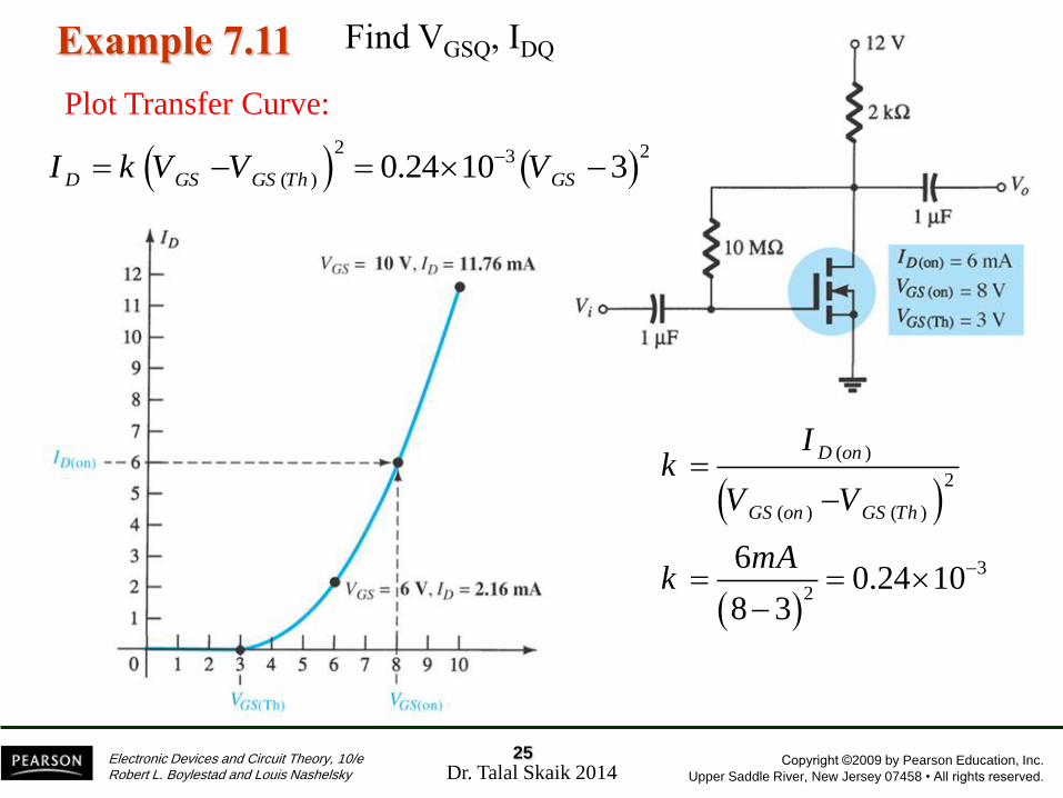
Example 7.11
25 Dr. Talal Skaik 2014
Find VGSQ, IDQ
( )
2
( ) ( )
3
2
60.24 10
8 3
D on
GS on GS Th
Ik
V V
mAk
2 23
( ) 0.24 10 3D GS GS Th GSI k V V V
Plot Transfer Curve:

Copyright ©2009 by Pearson Education, Inc.
Upper Saddle River, New Jersey 07458 • All rights reserved.
Electronic Devices and Circuit Theory, 10/e Robert L. Boylestad and Louis Nashelsky
Example 7.11 - solution
26 Dr. Talal Skaik 2014
Plot the line : VGS = VDD – IDRD
VGS = 12 – ID(2k)
Copyright ©2009 by Pearson Education, Inc.
Upper Saddle River, New Jersey 07458 • All rights reserved.
Electronic Devices and Circuit Theory, 10/e Robert L. Boylestad and Louis Nashelsky
Voltage-Divider Biasing
Plot the line and the transfer curve to find
the Q-point. Use these equations:
21
DD2G
RR
VRV
)RR(IVV
RIVV
DSDDDDS
SDGGS
27 Dr. Talal Skaik 2014
Copyright ©2009 by Pearson Education, Inc.
Upper Saddle River, New Jersey 07458 • All rights reserved.
Electronic Devices and Circuit Theory, 10/e Robert L. Boylestad and Louis Nashelsky
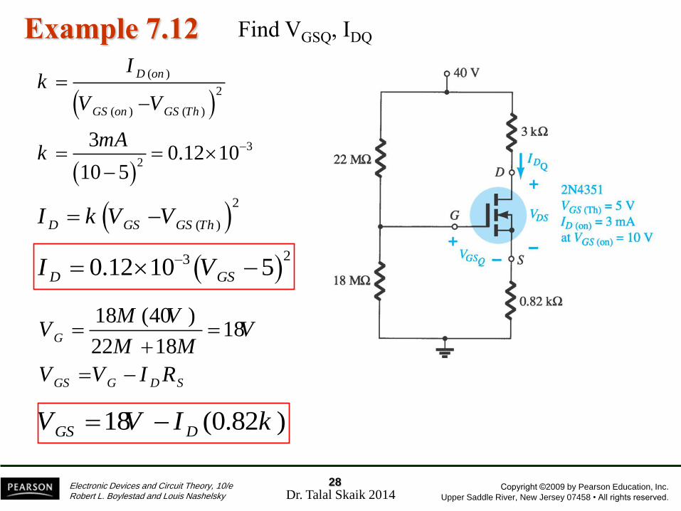
Example 7.12
28 Dr. Talal Skaik 2014
Find VGSQ, IDQ
( )
2
( ) ( )
3
2
30.12 10
10 5
D on
GS on GS Th
Ik
V V
mAk
2
( )D GS GS ThI k V V
230.12 10 5D GSI V
18 (40 )18
22 18G
GS G D S
M VV V
M M
V V I R
18 (0.82 )GS DV V I k

Copyright ©2009 by Pearson Education, Inc.
Upper Saddle River, New Jersey 07458 • All rights reserved.
Electronic Devices and Circuit Theory, 10/e Robert L. Boylestad and Louis Nashelsky
Example 7.12 - Solution
29 Dr. Talal Skaik 2014
230.12 10 5D GSI V 18 (0.82 )GS DV V I k