chapter i introduction 1. 1 introduction -...
TRANSCRIPT
1
Chapter I
Introduction
1. 1 Introduction:
Over the last decade use of microwave energy has become the emerging
field for a variety of applications. Different aspects of microwaves have been
applied in various branches of science and technology like industrial
measurements [1], medical and domestic applications [2], agricultural [3,4] etc.
Measurement of dielectric properties of moist biogranular materials such as
cereal grains and oil seed is essential for understanding their electrical
behaviour and the development of indirect nondestructive methods for
determining their physical characteristics including moisture content and bulk
density [5].
At microwave frequencies, dielectric properties of bio vegetation are
primarily a function of frequency, water saturation, porosity, texture,
component geometry and electrochemical interactions. Microwave techniques
and instrumentation can be utilized in agriculture to improve the efficiency of
the crop production, handling and processing, and improve the quality of the
products. Dielectric properties of agricultural materials and products are useful
in increasing numbers of applications, as new technology is adopted for use in
agriculture and related industries. Measuring and controlling moisture content
is an important aspect in the harvesting, storage marketing and processing of
oil seeds. The use of dielectric properties for measuring the moisture content of
products such as cereal grains has produced a variety of methods using the RF
range of electromagnetic radiation.
Recent airborne and deep space applications require the broadband and
real time dielectric characterization of the materials at microwave frequencies
apart from need of planarization. Microstrip components are very suitable to
overcome the planarization aspects of various microwave devices.
Agricultural biomaterials are materials consisting of organic and
inorganic inclusions along with water. Oil seeds form a major constituent of the
agricultural and food sector. The agricultural application of microwaves,
2
particularly crop growth studies like classification, mapping of various crops,
monitoring of crop growth parameters, leaf area index, moisture content, dry
matter production are very important aspect.
The present work deals with use of the Ag thick film microstripline
circuits in the Ku band (13-18 GHz) for dielectric characterization of moisture
laden oil seeds. This frequency band has been chosen because there are no
reports on use of microstrip components to study oilseeds in this frequency
range. In general, this frequency range is studied very less. Microwave
characterization and moisture content prediction at room temperature using Ag
thick film non resonant passive component has been done of three major seeds
(Soybean, Sunflower and Groundnut) having significant structural and
compositional differences. The moisture levels studied are those of interest to
the grain industry.
Thick film technology is a very cost effective technology [6,7] for
fabrication of miniaturized microwave components. The overlay technique has
been used to study the microwave characteristics of moisture laden oil seeds.
The change in the response of the Ag thick film microstrip passive components
has been used to characterize the moisture dependant microwave properties of
biomaterials (oil seeds). The thick film circuits fabricated and investigated
were Ag thick film microstripline of width 25 mil and Ag thick film equilateral
triangular microstrip patch antenna. All the designing, stencil preparation,
fabrication was done in the Thick and Thin Film Device Lab itself. The
samples of three different seeds (Soybean, Sunflower and Groundnut) of
Krishna Valley (grown at Sangli district in Maharashtra state of India in June-
Sept 2006) were used as overlay.
Apart from the overlay technique, waveguide reflectometer and VSWR
slotted line method was also used to characterize these moisture laden seeds at
various moisture levels. The calibration curve of the actual moisture content
versus measured moisture content from microwave measurement has been
plotted for the various seeds using the different measurement techniques.
3
1.2 Microwaves: Properties and applications:
Microwaves play an ever increasing role in modern life. The
electromagnetic spectrum from 300MHz to 300GHz is called the microwave
spectrum. This corresponds to the range of wavelength from 30 cm to 0.3 mm
in the free space. Microwaves occupy a region in the EM spectrum that is
bounded by radio waves on the side of longer wavelength and infrared waves
on the side of shorter wavelengths.
In this range many interesting properties of microwave radiations are
offered for a variety of applications [8],
1. Microwave radiation does not alter nor contaminate the material
under test, enabling fast, nondestructive and continuous monitoring.
2. Microwave can propagate through the free space allowing remote
sensing to be accomplished, where lower frequency signals gets
reflected from the ionosphere.
3. Relatively insensitive to environmental conditions like dust in
contrast to IR radiation.
4. Most of solid dielectric materials and atmosphere is transparent to
microwaves.
5. Large penetration depth compared to the IR radiation.
6. Microwaves are absorbed by the water and thus can be used to dry,
heat and cook food. Their absorption can be used to determine the
amount of moisture content within the materials.
7. Microwaves propagate along straight line.
Applications for which microwave provides moisture measurement are,
1. Pulp and paper manufacturing industries,
2. Packaging laminates
3. Sand and ceramics
4. Animal feed, powders and palletized product
5. Grain drying and agricultural harvesting and moisture measurement in
grain, leafy vegetation like tea, alfalfa etc.
6. Frozen food, fruit, milk processing and milk water measurement
4
7. Moisture in soil and wood measurement
8. Oil moisture measurement to detect good and bad oil.
The dimensions of microwave components are nearly equal to wavelength
and therefore new techniques and instruments are needed for dielectric
characterization of the materials in the microwave region of electromagnetic
spectrum.
For applications, the transmission structures for the microwave frequency range
includes wave-guides, open wire TEM lines, co-axial lines and planer
transmission structure which are the miniaturized version of transmission
structure.
1.3 Techniques for microwave measurements:
Various techniques can be used for measurement of microwave
properties of materials in the time and frequency domain. The correct choice
of microwave measurement techniques have to be made and various
restrictions exist in these techniques. The ideal method includes the following
merits,
1. It has good measurement accuracy for the properties.
2. The measurement procedures are simple and easy.
3. The required sample dimension is small.
4. The measurement frequency range is as wide possible and it has
the swept frequency capability.
At microwave frequencies, different measurement techniques can be
used [9,10].
• Transmission / reflection techniques (Waveguide, coaxial)
• Impedance bridge methods
• Cavity resonator methods
• Slotted line method
• Free space methods
• Overlay technique
5
All these methods fall into two categories: either destructive methods in
which sample preparation is needed for accurate evaluation or non destructive
methods which require very little or no sample preparation. In all these
methods the measured quantity enables the computation of its permittivity.
1.3.1 Transmission / reflection techniques [11-14]:
Transmission lines (waveguide) consisting of region between two
concentric cylinder (co-axial line) or the interior of hollow pipe (Rectangular or
circular waveguide) are used for measurements. Microwave signals are
propagated through these lines as electromagnetic waves and scattered from the
associated junction of these lines to travel in well-defined direction or ports.
Conventional open wire lines are unsuitable for microwave transmission
because of the high radiation losses that occur when the wavelength becomes
smaller than the physical lengths of these lines at high frequencies. The
structures [8] considered are:
1. Multi-conductor lines – coaxial lines, strip lines, microstriplines, slot lines
and coplanar lines.
2. Single conductor lines – rectangular waveguides, circular waveguides and
ridge waveguides.
3. Open boundary structures such as dielectric rods.
In the first category of lines, the mode of transmission is a TEM or
quasi- TEM wave. In the second category of lines, the modes are either TE or
TM waves or both. The third category of lines support, in general, a
combination of TE and TM waves called hybrid HE modes, expect possible
axis-symmetric modes which are either purely TE or TM waves.
The relation for input impedance, reflection coefficient, transmission
coefficient, characteristic impedance, all are applicable to microwave guides
operating in a single mode.
1.3.2 Impedance bridge methods
Microwave analogs of radio- frequency impedance bridges have been
6
constructed. These microwave bridges have the advantages that null detection
is used and uncertainties in the detector response law are unimportant.
However, impedance standards at microwave frequencies are difficult to
construct. Variable attenuators which serve as standards of resistance, have the
undesirable property of shifting the phase along the power level. Thus
reference elements of the bridge must be calibrated by another method before
one can take advantage of the speed of measurement possible with the bridge
methods.
Most bridges are usually of symmetrical structures, to simplify the
balance equations. Much of the simplicity introduced by symmetry is lost in
practice because of fringing fields and associated frequency dependent
reactance between the arms of the bridge for comparing transmitted waves. At
the single frequency, the symmetry may be restored by means of appropriate
matching devices. Waveguide along of r-f impedance bridge was described by
[10] who constructed a waveguide bridge for measurement of dielectric loss of
dilute solution.
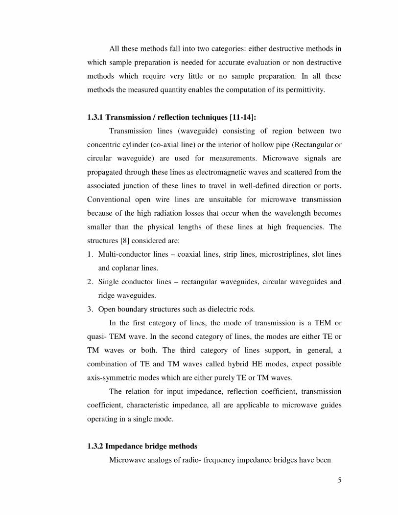
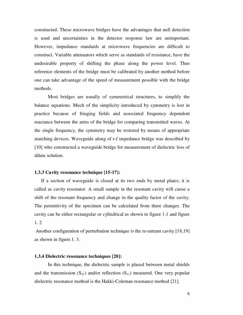
1.3.3 Cavity resonance technique [15-17]:
If a section of waveguide is closed at its two ends by metal plates; it is
called as cavity resonator. A small sample in the resonant cavity will cause a
shift of the resonant frequency and change in the quality factor of the cavity.
The permittivity of the specimen can be calculated from there changes. The
cavity can be either rectangular or cylindrical as shown in figure 1.1 and figure
1. 2
Another configuration of perturbation technique is the re-entrant cavity [18,19]
as shown in figure.1. 3.
1.3.4 Dielectric resonance techniques [20]:
In this technique, the dielectric sample is placed between metal shields
and the transmission (S21) and/or reflection (S11) measured. One very popular
dielectric resonance method is the Hakki-Coleman resonance method [21].
7
Rectangular waveguide cavity
Specimen
Fig. 1.1 TE cavity perturbation technique.
Cylindrical metal cavity specimen
Fig. 1.2 TM cavity perturbation technique.
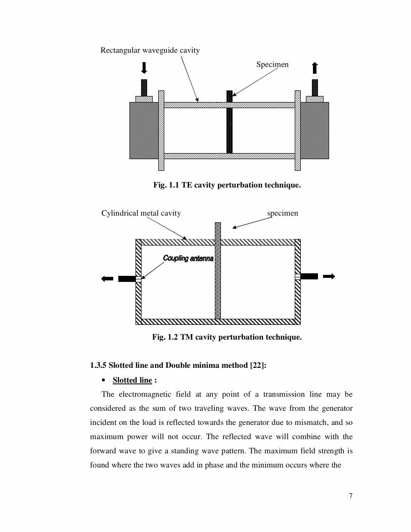
1.3.5 Slotted line and Double minima method [22]:
• Slotted line :
The electromagnetic field at any point of a transmission line may be
considered as the sum of two traveling waves. The wave from the generator
incident on the load is reflected towards the generator due to mismatch, and so
maximum power will not occur. The reflected wave will combine with the
forward wave to give a standing wave pattern. The maximum field strength is
found where the two waves add in phase and the minimum occurs where the
-
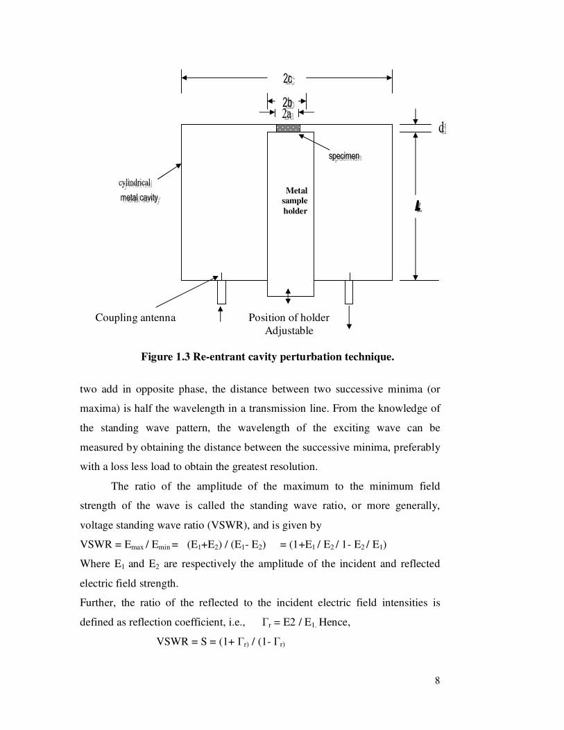
8
Coupling antenna Position of holder
Adjustable
Figure 1.3 Re-entrant cavity perturbation technique.
two add in opposite phase, the distance between two successive minima (or
maxima) is half the wavelength in a transmission line. From the knowledge of
the standing wave pattern, the wavelength of the exciting wave can be
measured by obtaining the distance between the successive minima, preferably
with a loss less load to obtain the greatest resolution.
The ratio of the amplitude of the maximum to the minimum field
strength of the wave is called the standing wave ratio, or more generally,
voltage standing wave ratio (VSWR), and is given by
VSWR = Emax / Emin = (E1+E2) / (E1- E2) = (1+E1 / E2 / 1- E2 / E1)
Where E1 and E2 are respectively the amplitude of the incident and reflected
electric field strength.
Further, the ratio of the reflected to the incident electric field intensities is
defined as reflection coefficient, i.e., Гr = E2 / E1. Hence,
VSWR = S = (1+ Гr) / (1- Гr)
Metal
sample
holder
9
When Emin = Emax i.e. there is no reflection [E2 = 0], the resulting VSWR = 1,
this is the requirement of a mached circuit. In other words, under given ideal
conditions, the VSWR of a mached load is 1.00. Under extreme mismatch
conditions, Emin = 0, i.e. total reflection, [E2 = E1], the resulting VSWR = ∞.
However, in most of the cases, VSWR > 1. It is not rare to obtain VSWR as
low as 1.02 in well designed set up having matched components.
Thus the degree of mismatch between the load and the transmission line
can be calculated from the measurement of VSWR. Complex load will also
shift the phase and hence minimum position, so load impedance can be
calculated from the VSWR and the position of the minimum point on the line
with respect to the load.
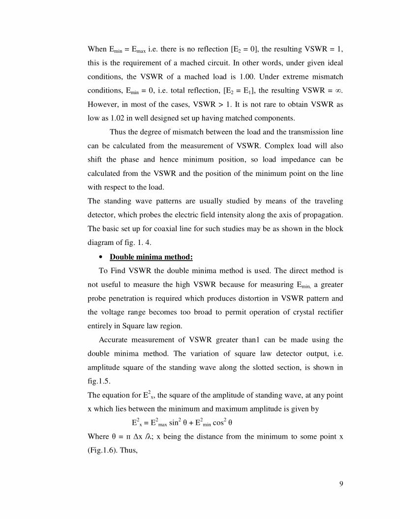
The standing wave patterns are usually studied by means of the traveling
detector, which probes the electric field intensity along the axis of propagation.
The basic set up for coaxial line for such studies may be as shown in the block
diagram of fig. 1. 4.
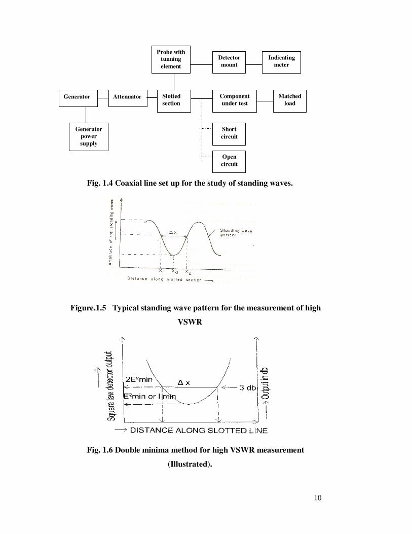
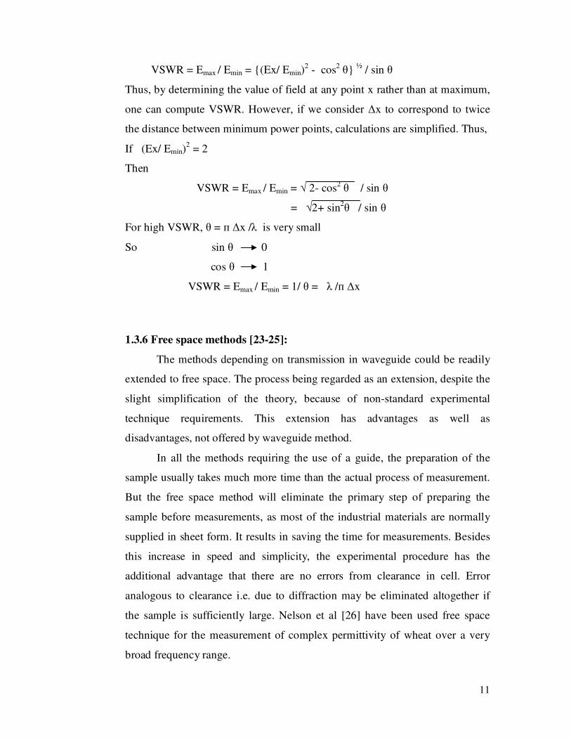
• Double minima method:
To Find VSWR the double minima method is used. The direct method is
not useful to measure the high VSWR because for measuring Emin, a greater
probe penetration is required which produces distortion in VSWR pattern and
the voltage range becomes too broad to permit operation of crystal rectifier
entirely in Square law region.
Accurate measurement of VSWR greater than1 can be made using the
double minima method. The variation of square law detector output, i.e.
amplitude square of the standing wave along the slotted section, is shown in
fig.1.5.
The equation for E2
x, the square of the amplitude of standing wave, at any point
x which lies between the minimum and maximum amplitude is given by
E2
x = E2
max sin2 θ + E
2min cos
2 θ
Where θ = п ∆x /λ; x being the distance from the minimum to some point x
(Fig.1.6). Thus,
10
Fig. 1.4 Coaxial line set up for the study of standing waves.
Figure.1.5 Typical standing wave pattern for the measurement of high
VSWR
Fig. 1.6 Double minima method for high VSWR measurement
(Illustrated).
Generator Attenuator Slotted
section
Component
under test
Matched
load
Generator
power
supply
Probe with tunning
element
Detector
mount
Indicating
meter
Short
circuit
Open
circuit
11
VSWR = Emax / Emin = (Ex/ Emin)2 - cos
2 θ
½ / sin θ
Thus, by determining the value of field at any point x rather than at maximum,
one can compute VSWR. However, if we consider ∆x to correspond to twice
the distance between minimum power points, calculations are simplified. Thus,
If (Ex/ Emin)2 = 2
Then
VSWR = Emax / Emin = √ 2- cos2 θ / sin θ
= √2+ sin2θ / sin θ
For high VSWR, θ = п ∆x /λ is very small
So sin θ 0
cos θ 1
VSWR = Emax / Emin = 1/ θ = λ /п ∆x
1.3.6 Free space methods [23-25]:
The methods depending on transmission in waveguide could be readily
extended to free space. The process being regarded as an extension, despite the
slight simplification of the theory, because of non-standard experimental
technique requirements. This extension has advantages as well as
disadvantages, not offered by waveguide method.
In all the methods requiring the use of a guide, the preparation of the
sample usually takes much more time than the actual process of measurement.
But the free space method will eliminate the primary step of preparing the
sample before measurements, as most of the industrial materials are normally
supplied in sheet form. It results in saving the time for measurements. Besides
this increase in speed and simplicity, the experimental procedure has the
additional advantage that there are no errors from clearance in cell. Error
analogous to clearance i.e. due to diffraction may be eliminated altogether if
the sample is sufficiently large. Nelson et al [26] have been used free space
technique for the measurement of complex permittivity of wheat over a very
broad frequency range.
12
1.3.7 Overlay technique [27-29]:
A new technique, which employs a microwave microstripline
component in the multilayer (overlay) configuration as a nondestructive and
miniaturized novel sensor, has been recently developed. The loading and
unloading of the samples is facilitated by its open structure.
If the microstrip component is a resonating circuit, a shift in the
resonance frequency is observed which can be translated into the overlay
material property. If it is a non resonating circuit, the changes in reflectance
and transmittance can be converted into the material properties. The various
types of microstrip components that can be used for overlay technique are
simple microstripline, λ/2 rejection filter, ring resonator, straight resonator and
patch antenna. All these components being in the planar form, miniaturize
sensors can be fabricated.
1.4 Microwave Methods for Agricultural biogranular material:
Farming is one of the oldest and most important human activities and
food production is essential to man’s survival. Intrinsic nature of the complex
permittivity makes it the best entity to describe the wave–material interaction.
The moist granular substances are mixtures of components exhibiting different
dielectric behaviors, it is rather difficult to use the measured complex
permittivity directly for moisture content. Characterization of dependence of
dielectric properties of the seed to its moisture content is an important step in
this endeavor. The seed show wide range of variation in shape, size, internal
characteristics depending on the chemical composition of seeds that are
different due to nutrition, stress, water, soil etc. Many food and agricultural
products are granular. Therefore, in addition to moisture content, bulk density
and other factors such as geometry and dimensions of the granular particles
affect the complex permittivity.
Though a number of reports [30-33] are available for use of microwaves
for biovegetation and biomaterials, only those work dealing with seeds have
been referenced in this thesis. Dielectric properties of materials can be useful
13
for nondestructive, continuous determination of important characteristics such
as the moisture content and bulk density of agricultural and food products. For
food and agricultural products, the permittivity is the effective permittivity of a
mixture of components with different dielectric behaviours. Microwaves can be
used in the active and passive mode.
Microwave energy can be used in two different ways for moisture
content determination in agricultural products. The correlation of dielectric
properties with moisture content permits the sensing of moisture through
electronic measurement of related quantities and other is the rapid drying of
samples in microwave ovens to low levels and determining moisture content by
sample weight loss and calibrating to a standard air or vacuum oven method
[34]. The standard oven method requires high temperature and long time and
also they are not useful for on-line process.
Of all the microwave applications to agricultural biomaterial moisture
content determination has the longest and most successful history and the most
promising perspectives.
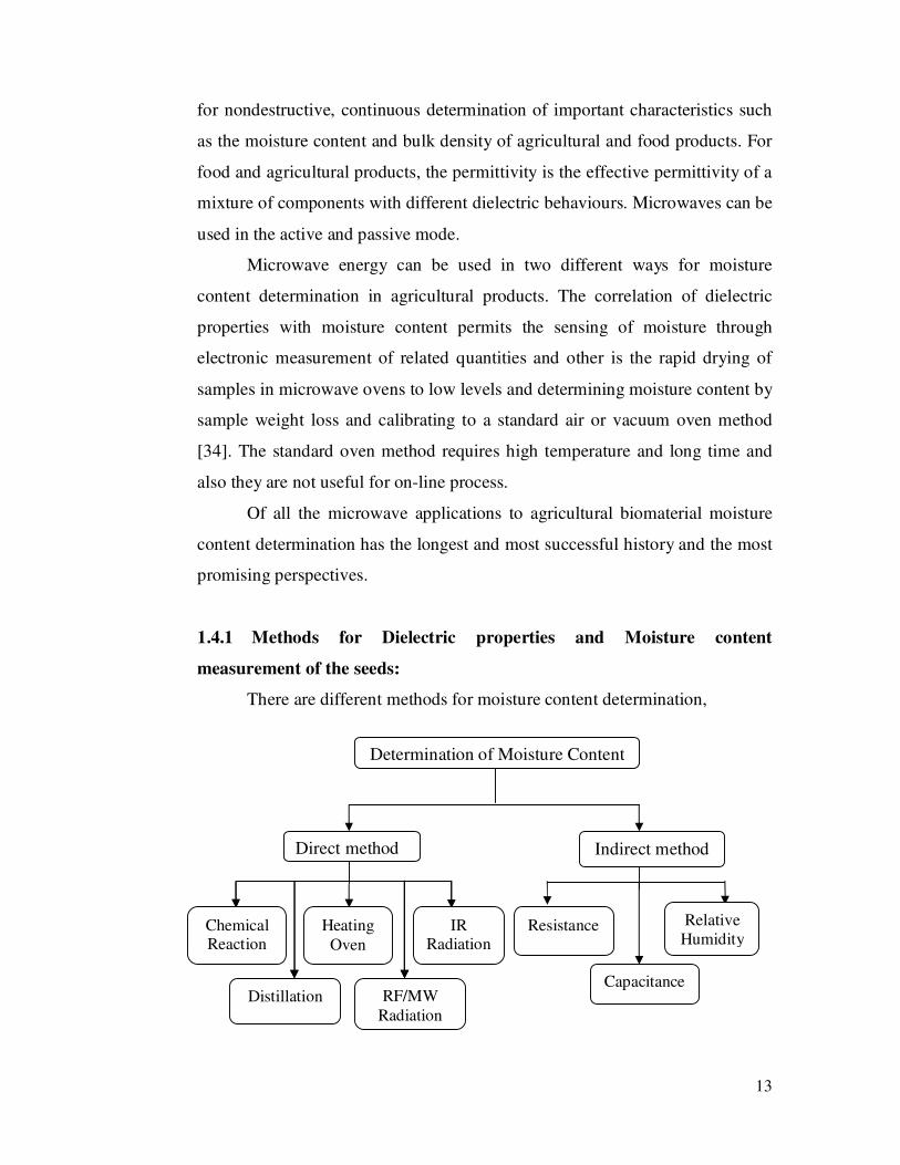
1.4.1 Methods for Dielectric properties and Moisture content
measurement of the seeds:
There are different methods for moisture content determination,
Determination of Moisture Content
Indirect method
Capacitance
Relative
Humidity
Distillation
Resistance
RF/MW
Radiation
Direct method
Chemical Reaction
IR Radiation
on
Heating
Oven
14
Water is an important component of many natural and man made
material. Understanding water behaviour is fundamental in improving and
preserving the quality of many of the materials.
Moisture content of cereal grains and seeds is one of the most important
characteristics determining quality, proper time for harvest, the potential for
safe storage and selling price because the dry matter of grain has more value
than the water it contains and because costs of drying must be taken into
account when grain must be dried to safe storage levels. Rapid determination of
moisture content in the natural and manufactured products is important for
process and quality control.
In this work microwaves have been used to characterize the
seeds, the various dielectric properties and moisture content determination
techniques have been divided into non radio frequency technique and radio
frequency technique.
1.4.1.1 Non radio frequency techniques:
This article reviews the various non radio frequency techniques for
permittivity and moisture content measurement in brief.
Air-oven method is the most common reference method for grain
moisture determination. Other methods such as phosphorous pentoxide (P2O5)
method [35] and Karl-Fischer titration method [36] are also used. These
methods provide accurate results for moisture content but are very time
consuming and require various chemicals. Electronic moisture meters have
been used to determine moisture content in sunflower [37]. Low resolution
NMR has also been used to simultaneously determine water and oil content in
seeds [38]. Near IR transmittance and reflectance technology has also been
used for the analysis of grains and seeds [39- 43].
1.4.1.2 RF/ Microwave techniques:
Compared to direct techniques indirect techniques are more suited for
rapid determination of moisture content for automated industrial process and
15
the growing need for real time decision making. Radiation based methods offer
on-line processing.
Nuclear- type sensors are expensive and present potential hazards. IR
sensors are limited to sensing surface moisture content. The RF and microwave
techniques have emerged as an alternative for rapid and non destructive sensing
of moisture.
Various attempts have been made to correlate the electrical properties of
agricultural products with moisture content. At microwave frequencies, the
electromagnetic energy is mainly absorbed by water. This selective absorption
is mainly due to the polar character of water molecules and their high
permittivity compared with that of dry matter.
The moisture content of material ‘M’ is expressed as [44]
M (%) = MdMw
Mw
+ X 100 ....................... 1.1
Where Mw = mass of water
Md = mass of dry material
Interaction of EM waves with wet material takes place at sensor. Many
radiating elements in waveguide, co-axial line or strip line configurations can
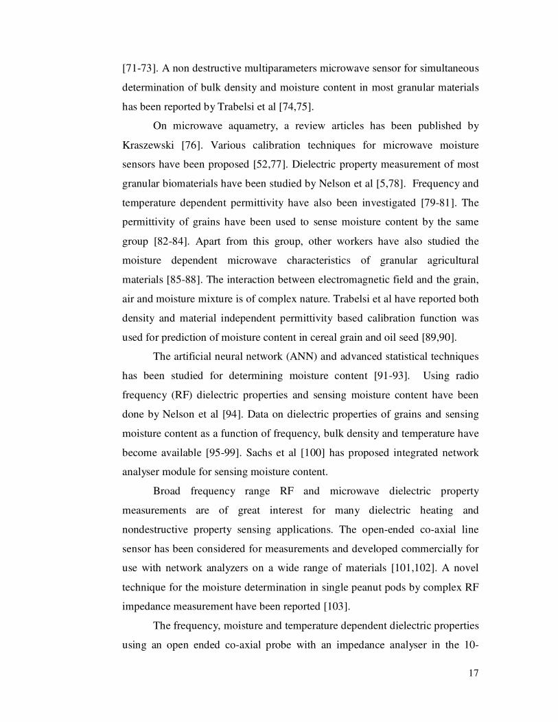
be used as sensors. Some examples of sensors are shown in fig. 1.7.
Dielectric based sensors are divided according to their operating
frequency at two classes: MHz frequency and GHz frequency. The sensors are
divided into resonant and periodic groups, into open and close structures and
into reflection and transmission types. Output of sensor is function of material
characteristics. The parameters like absorption in material, attenuation, phase
shift, reflection coefficient, and resonant frequency can be used to measure the
moisture content. All these parameters can be measured on the basis of
deflection, null method including substitution, comparison and compensation
methods.
The group of S. O. Nelson, S. Trabelsi, and A. W. Kraszewski have used
waveguide technique, free space method and resonator method for studying a
16
variety of biomaterials. A large number of publications exists of this group.
Only those published in the last 15 years have been included in this thesis.
Determining moisture content in granular and particulate materials from
measurement of microwave parameters at a single frequency or several
frequencies requires compensation for, or elimination of temperature and bulk
density effects [45]. Jacobsen et al [46] have proposed the first density-
independent calibration function for moisture content determination from
permittivity data. It was later tested by others [47-51] for a large variety of
granular and particulate materials.
Success of microwave sensing is related to the polar nature of the water
molecule and its high dielectric constant (~80). Both ε’ and ε” are intrinsic
properties of the material and both depend on frequency, temperature, moisture
content and for granular material, they also depend on bulk density [45,52]. At
higher frequencies, bulk density effect eliminates and compensate for
temperature effects [53]. Bulk density measurement is more troublesome and
several density independent algorithms [54-65] for moisture sensing in granular
and particulate materials have been proposed. For prediction of moisture
content density independent calibration functions were used in shelled peanuts
from free space measurements [66]. A unified method for moisture sensing in
cereal grain and oil seed has been reported by S. Trabelsi et al [67].
Funk et al [68] has reported the RF impedance material analyser and
various grains models were developed to predict unifying calibration
parameters and temperature correction coefficient from the chemical and
physical properties of grains.
The various microwave techniques in agriculture has been explained by
Kraszewski et al [8]. RF impedance method have proved to be nondestructive
method for moisture content determination for in-shell peanuts [69] by Kandala
et al. Nonequilibrated water has been used for sensing moisture content on
microwave dielectric properties of wheat and related errors[70]. Microwave
permittivity measurements on unshelled pod useful in non-destructive and
simultaneous determination of moisture have been reported by Trabelsi et al
17
[71-73]. A non destructive multiparameters microwave sensor for simultaneous
determination of bulk density and moisture content in most granular materials
has been reported by Trabelsi et al [74,75].
On microwave aquametry, a review articles has been published by
Kraszewski [76]. Various calibration techniques for microwave moisture
sensors have been proposed [52,77]. Dielectric property measurement of most
granular biomaterials have been studied by Nelson et al [5,78]. Frequency and
temperature dependent permittivity have also been investigated [79-81]. The
permittivity of grains have been used to sense moisture content by the same
group [82-84]. Apart from this group, other workers have also studied the
moisture dependent microwave characteristics of granular agricultural
materials [85-88]. The interaction between electromagnetic field and the grain,
air and moisture mixture is of complex nature. Trabelsi et al have reported both
density and material independent permittivity based calibration function was
used for prediction of moisture content in cereal grain and oil seed [89,90].
The artificial neural network (ANN) and advanced statistical techniques
has been studied for determining moisture content [91-93]. Using radio
frequency (RF) dielectric properties and sensing moisture content have been
done by Nelson et al [94]. Data on dielectric properties of grains and sensing
moisture content as a function of frequency, bulk density and temperature have
become available [95-99]. Sachs et al [100] has proposed integrated network
analyser module for sensing moisture content.
Broad frequency range RF and microwave dielectric property
measurements are of great interest for many dielectric heating and
nondestructive property sensing applications. The open-ended co-axial line
sensor has been considered for measurements and developed commercially for
use with network analyzers on a wide range of materials [101,102]. A novel
technique for the moisture determination in single peanut pods by complex RF
impedance measurement have been reported [103].
The frequency, moisture and temperature dependent dielectric properties
using an open ended co-axial probe with an impedance analyser in the 10-
18
1800MHz range has been reported [104]. Dielectric properties of seeds using
parallel plate capacitor in the 50 KHz-100MHz have been investigated by
Sacilik et al [105,106].
Fig. 1.7 Classification of Microwave sensors being used for moisture
content meter
Gillay et al has reviewed prediction equation relative to dielectric
constant to moisture content developed for a range of RF higher measurement
frequency yielded smaller predicted moisture difference than lower frequency
studies on corn [107]. The use of overlay technique to study biomaterials has
been done by group at Pune University and in our lab. The Pune University
group mainly used the thin film microstrip ring resonator in the X-band, where
as in this work the thick film resonant and non resonant microstrip components
have been used. There are very few works available for the seeds using
microstripline components. The permittivity aspects of these biomaterials are
also not explained in detail using this technique.
The use of thin film microstrip ring resonator as a moisture sensor in
wheat grains [108], chickpea [109], mug grains [110], feasibility study of a
novel moisture sensor microstripline component also [111,112] have been
reported. All this work is in the X band (8-12GHz). The size dependent leaf
overlay effects on thin film microstrip patch antenna has also been studied
[113]. A comparative study of thin film and thick film component response to
19
leaf overlay has been reported by Ghorpade et al [114-116]. The moisture
dependent leaf overlay effects on thick film microstrip components has also
been studied by Kamble et al [117-118]. The limited studies on moisture laden
seeds using microstrip components indicates the scope for further studies of
these components to be used for biogranular material characterization.
1.5 Microwave Transmitting Structures: A Brief Introduction
The waveguide components, a simple Ag thick film microstripline
and thick film equilateral triangular microstrip patch antenna were used,
therefore only those structures are elaborated in the proceeding articles.
1.5.1 Transmission and reflection parameters:
At microwave frequency, the operational wavelength becomes
comparable to the dimensions of the device geometries. It is more appropriate
to consider the response of a component in the path of microwaves as it
propagates through a transmission medium. The components at microwave
frequency can be characterized by various transmission and reflection
parameters.
The important transmission/reflection parameters include-
1. Transmission coefficient
2. Reflection coefficients
3. Insertion loss / Gain
4. Standing wave ratio
In this work rectangular waveguide with sample kept transverse to the
direction of propagation has been used. The theory of propagation of
microwave through rectangular waveguide in given in brief in the next article.
1.5.1.1 Rectangular waveguide:
Microwave signals were traditionally transmitted through hollow metal
pipes called waveguides. Wave bounce back and forth from the conductor
walls, producing signal propagation when frequencies exceed a lower bound
20
called cut off frequency. Metal waveguides are inherently rigid that is the
realization of waveguide circuits leads to some interesting topological
problems. The circuit themselves tend to be rather heavy and bulky.
Waveguides are therefore used mainly where high power operation is required
and at the upper limit of microwave range (millimeter range).
Rectangular waveguides were one of the earliest types of transmission
lines used to transport microwave signals and are still used today for many
applications. A large variety of components such as couplers, detectors,
isolators, attenuators and slotted lines are commonly available for various
standard waveguide bands from 1 GHz to over 220 GHz.
(The hollow rectangular waveguide can propagate TM and TE modes,
but not TEM waves, since only one conductor is present.)
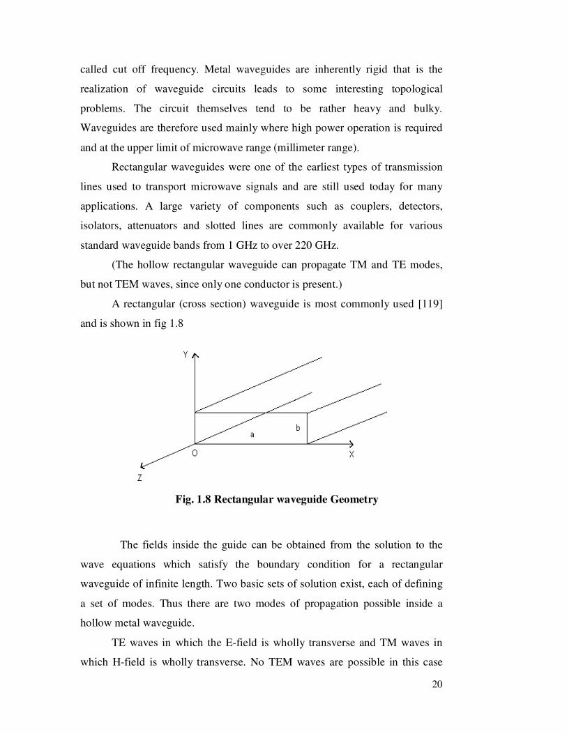
A rectangular (cross section) waveguide is most commonly used [119]
and is shown in fig 1.8
Fig. 1.8 Rectangular waveguide Geometry
The fields inside the guide can be obtained from the solution to the
wave equations which satisfy the boundary condition for a rectangular
waveguide of infinite length. Two basic sets of solution exist, each of defining
a set of modes. Thus there are two modes of propagation possible inside a
hollow metal waveguide.
TE waves in which the E-field is wholly transverse and TM waves in
which H-field is wholly transverse. No TEM waves are possible in this case
21
since it require an axial conductor for axial current flow or an axial
displacement current (axial E field) to support a transverse magnetic field.
For an infinite guide and propagation along the Z-direction
)( zjK ze−
the wave equations are:
∇2E+K
2E = 0 1.2
∇2H+K
2H = 0 1.3
This can be written as,
TM : 022 =+∇ ZCZt EKE 1.4
TE : 022 =+∇ZCZt HKH 1.5
Where
2
2
2
2
yxt
∂
∂+
∂
∂=∇ and
Kc = 22
zKK − = 22
yx KK − = cλ
π2 1.6
and is called the cut off wave number. The propagation constant in the guide is,
therefore,
22
CZ KwjK −±= µε 1.7
There are three special cases apparent
1. For no propagation (evanescent mode) to take place Kz = 0 or
Kc= wc µε Here wc is the cut off frequency in radian/sec.
2. For propagation of real power, Kz > 0 or w µε > Kc
3. If wc µε < Kc, Kz is imaginary ( j∝), so that the wave will be
attenuated in accordance with e-∝z
.
1.5.1.2 TE waves solution:
For TE waves propagating in + Z direction Ez = O, and solution may be
derived from the Hz component of equation (1.5)
Hz = COS
a
xmπCOS
b
ynπ 1.8
22
This satisfies the boundary condition of the walls. Harmonic solution in
the x and y directions show that the waves produce a standing wave between
the longitudinal walls, giving the values Kx = a
mπ and
Zjk
yze
b
nK
−=π
factor is omitted but this is present in all field components.
Here m = 0, 1, 2 ----- denotes the number of half waves in the x direction and n
= 0, 1, 2 ----- those in the y direction, when m # n = 0. To each set of integer’s
m and n a solution exists, and these modes are designed as the TEmn modes.
The other field components are obtained form the Maxwell’s equation as
follows.
b
ynSin
a
xmCOS
b
n
K
jKH
C
Z
y
πππ2
= 1.9
b
ynCOS
a
xmSin
a
m
K
jKH
C
Zx
πππ2
= 1.10
Ez = 0 1.11
E y = Kz
ωµH x 1.12
E x = Kz
ωµ H y 1.13
The cut-off frequency and cut-off wavelength as defined in equation for
the TEmn modes are,
22
2
1
+
=
b
n
a
mF C
µε 1.14
22
2
−
=
b
n
a
mcλ
1.15
The propagation constant is expressed by,
2
1
−==
ω
ωµεωβ C
ZK 1.16
The phase velocity of the waves
23
2
1
−
==
f
f
uu
C
pβ
ω 1.17
Where u = µε
1, the phase velocity in an unbounded dielectric (µ,ε).
The velocity of energy propagation called the group velocity is given by,
p
gu
uV
2
= 1.18
the propagation wavelength inside the guide is called the guide wavelength and
is given by,
2
1
1
−
=
c
g
λ
λλ 1.19
Where, λ = f
µ, the wavelength in an unbounded dielectric.
The characteristic wave impendence in the guide can be derived as, for TEmn
mode.
02
377
1λ
λη
ββ
ωµ g
cX
Y
Y
Xw
f
f
nk
H
E
H
EZ =
−
===−== ohm 1.20
where η = ε
µ is the intrinsic impedance in an unbounded dielectric.
1.5.1.3 TM Waves Solution
The TM waves propagating in +z direction are characterized by Hz = 0.
A Field solution to equation (1.4) gives
E z = Sin
a
xmπsin
b
ynπ 1.21
=
b
ynCos
a
xmSin
bk
kjnE
c
zY
πππ2
1.22
=
b
ynSin
a
xmCos
ak
kjmE
c
z
X
πππ2
1.23
24
Hz = 0 1.24
H y = Kz
ωεEx 1.25
H x = - Kz
ωεEy 1.26
Where m = 1,2,3…. And n = 1,2,3….. Here m or n # O, since either
m=0 or n=0 leads to zero field intensities. For TMmn modes, the equations for
the cut off frequency fc, propagation constant β, the phase and group velocities
up and ug, and the guide wavelength λg are the same as those for TEmn modes
given in equation (1.14) to (1.19).
The characteristics wave impedance is given by,
ohmf
f
k
n
H
E
H
EZ
g
c
X
Y
Y
Xw λ
λη
β
ωε
β 0
2
3771 =
−===−== 1.27
TE10 mode is a simple and useful field distribution, has minimum
attenuation arising from various factors. The ribs of the waveguide operating
on TE10 mode carry the maximum transverse current, consequently, a very
good electric contact between the waveguide walls at the ribs has to be insured,
if hole is fabricated from the separate strip of metal, size the TE10 mode is
dominant in rectangular waveguide.
1.5.2 Transmission lines for Planar MIC:
Planar transmission lines are those in which the entire transmission line
components can be fabricated in one step by thin film or photolithographic
techniques. A transmission line is made up of a symmetrical pair of strip
conductor or a single strip and ground plane, at opposite face to of sheet of
dielectric material. These techniques are simple methods for broadband
characterization. Transmission lines [120-121] can be in the form of
microstripline, slot line, coplanar waveguide and many other types of related
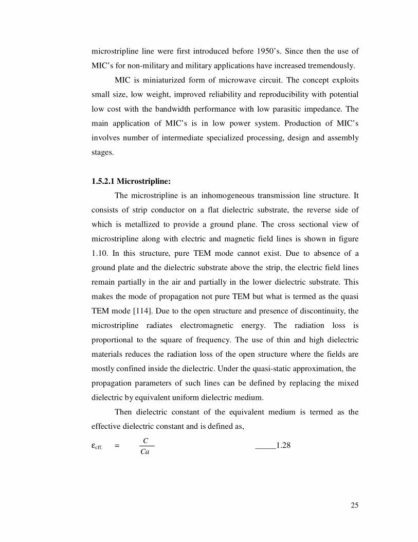
geometries as shown in figure 1.9. Mostly they are made of conducting strips
deposited on dielectric substrate along with other active and passive
components they are called microwave integrated circuits [MIC]. Strip line and
25
microstripline line were first introduced before 1950’s. Since then the use of
MIC’s for non-military and military applications have increased tremendously.
MIC is miniaturized form of microwave circuit. The concept exploits
small size, low weight, improved reliability and reproducibility with potential
low cost with the bandwidth performance with low parasitic impedance. The
main application of MIC’s is in low power system. Production of MIC’s
involves number of intermediate specialized processing, design and assembly
stages.
1.5.2.1 Microstripline:
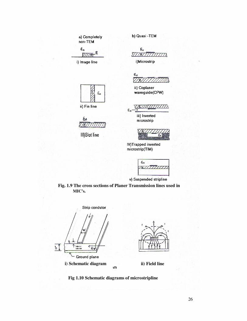
The microstripline is an inhomogeneous transmission line structure. It
consists of strip conductor on a flat dielectric substrate, the reverse side of
which is metallized to provide a ground plane. The cross sectional view of
microstripline along with electric and magnetic field lines is shown in figure
1.10. In this structure, pure TEM mode cannot exist. Due to absence of a
ground plate and the dielectric substrate above the strip, the electric field lines
remain partially in the air and partially in the lower dielectric substrate. This
makes the mode of propagation not pure TEM but what is termed as the quasi
TEM mode [114]. Due to the open structure and presence of discontinuity, the
microstripline radiates electromagnetic energy. The radiation loss is
proportional to the square of frequency. The use of thin and high dielectric
materials reduces the radiation loss of the open structure where the fields are
mostly confined inside the dielectric. Under the quasi-static approximation, the
propagation parameters of such lines can be defined by replacing the mixed
dielectric by equivalent uniform dielectric medium.
Then dielectric constant of the equivalent medium is termed as the
effective dielectric constant and is defined as,
εcff. = Ca
C _____1.28
26
Fig. 1.9 The cross sections of Planer Transmission lines used in
MIC’s.
Fig 1.10 Schematic diagrams of microstripline
i) Schematic diagram
ii) Field line
27
Where, C is capacitance per unit length of transmission line and Ca capacitance
per unit length with all dielectric replaced by air.
The phase velocity V, guided wave length gλ and characteristic impedance Z
are given by,
V = 2
1
.)( eff
Va
ε ____ 1.29
gλ = 2
1
)( eff
a
ε
λ ____ 1.30
21
21
01
)()( eff
g
eff
zZ
ε
λ
ε= ____ 1.31
Here Eeff is effective dielectric constant of the medium and its values lies in the
range 1 < εeff < εr Z01 is the characteristic impedance of microstrip line with
dielectric replaced by air.
1.5.2.2 Synthesis formulae (Z0 and rε given):
For narrow strips [i.e. when Z0 > 44 - 2 rε ohms]:
1
'exp4
1
8
'exp−
−
=
H
H
h
W ------- 1.32
Where
( )
+
+
−+
+=
πε
π
ε
εε 41
21
1
2
1
9.119
12'
0InIn
ZH
rr
rr ------- 1.33
We may also use, with slight but significant shift of changeover value to
W/h < 1.3 (i.e. when Z0 > 63 – 2 rε ohms) :
2
41
21
1
'2
11
2
1−
+
+
−−
+=
πε
π
ε
εεε InIn
H rr
rreff ------ 1.34
Where H’ is given by equation (1.33) (as a function of Z0) or, alternatively, as a
function of W/h, from equation (1.32):
28
+
+= 2164'
2
W
h
W
hInH ------- 1.35
Another, somewhat simpler, expression for effε (Z0) is given by Owens is,
2
2
1
0
41
21
1
1
298.291
2
1
+
+
−
++
+=
πε
π
ε
ε
ε
εε InIn
Z rr
r
r
reff ------- 1.36
Now consider the ranges and formulae for “Wide” strips.
For wide strips (i.e. when Z0 < 44 – 2 rε ohms) :
( ) ( ) ( )
−+−−
+−−−=rr
r dIndIndh
W
εε
πε
εεε
π
517.0293.01
1121
2 ------- 1.37
Where
rZd
ε
π
0
295.59= ------- 1.38
With the same slight shift of changeover value as before (i.e. where W/h > 1.3
and Z0> 63-2rε ohms) Owens found that a modified form of an earlier
expression due to Schneider gave very accurate results. Owens’s [122] formula
is :
555.0
1012
1
2
1−
+
−+
+=
W
hrr
eff
εεε ------- 1.39
Alternatively, where Z0 is known at first
( ) ( ) 110log004.0109.096.0 0 −+−+=
Zrr
r
effεε
εε ------- 1.40
For microstriplines on alumina ( rε = 10 ) this expression appears to be
accurate to ± 0.2 percent over the impedance range 8 ≤ Z0 ≤ 45 Ω
1.5.2.3 Analysis Formulae (h
W and rε given):
For ‘narrow’ strips (h
W < 3.3) :
29
( )
+
+
−−
+
+
+=
πε
π
ε
ε
ε
41
21
1
2
12164
12
9.1192
0 InInW
h
W
hInZ
rr
r
r
---1.41
For ‘wide’ strips (h
W > 3.3):
1
2
2
0 94.0222
11
2
164
22
9.119
−
++
++
−
++=h
WIn
eIn
eIn
In
h
WZ
r
r
r
r
r
π
πε
ε
ε
ε
π
π
πε
π
------- 1.42
Where, ‘e’ is the exponential base: e = 2.7182818 ----
In all cases the shape ratio W/h will be accurate to ± 1%. For narrow lines
(W/h < 1/3), effε has the error range of + 0.5 – 0.0%. When calculated using
equation (1.39), effε is accurate to ± 0.25%. The expressions for Z0 result
inaccuracies to ± 1%.
The characteristic parameters of microstripline depend on strip width
‘W’, thickness ‘h’ and the dielectric constant rε of the substrate. For a given
thickness and dielectric constant of the substrate, strip width controls the
characteristics of the line. This feature makes microstriplines well suited for
MIC’s.
The microstrip synthesis consists of finding the values of width ‘W’ and
length ‘L’ corresponding to the characteristic impedance Z0 and electrical
length ‘θ ’. Initially a substrate of thickness ‘h’ and relative permittivity rε
has to be chosen. The choice depends upon certain frequency limitations.
Initially the synthesis yield W/h ratio and effective microstrip permittivity effε
from the other design parameters can be determine [122,123]. Most of the
synthesis available is for substrates with rε less than 15. Recently Crute [124]
has investigated properties of high rε microstrip lines.
1.5.2.4 Effective dielectric constant of microstripline:
Since the propagation field lines in a microstrip lie partially in air and
partially inside the homogenous dielectric substrate, the propagation delay time
30
for a quasi-TEM mode is related to an effective dielectric constant εeff [121]
given by,
−+
+
−+
+=
−2
2
1
104.012
12
1
2
1
h
w
w
hrreff
εεε 1; ≤
h
w 1.43
and2
1
121
2
1
2
1−
+
−+
+=
w
hrreff
εεε 1; >>
h
w 1.44
+=
h
w
w
hInZ
eff4
80
0ε
σ Ohm 1; ≤h
w 1.45
Where, εr is the relative dielectric constant of the substrate material.
Characteristic impedance and guide wavelength:-
Characteristics impedance of microstrip lines [121] can be expressed by,
+++
=
444.1667.04.1
7.3760
h
wIn
h
wZ
effε
Ohm 1; >h
w 1.46
w
hZ
effε
7.3760 = Ohm 1; >>
h
w 1.47
The guide wavelength for the propagation of quasi-TEM mode is given by,
eff
g
ε
λλ 0= 1.48
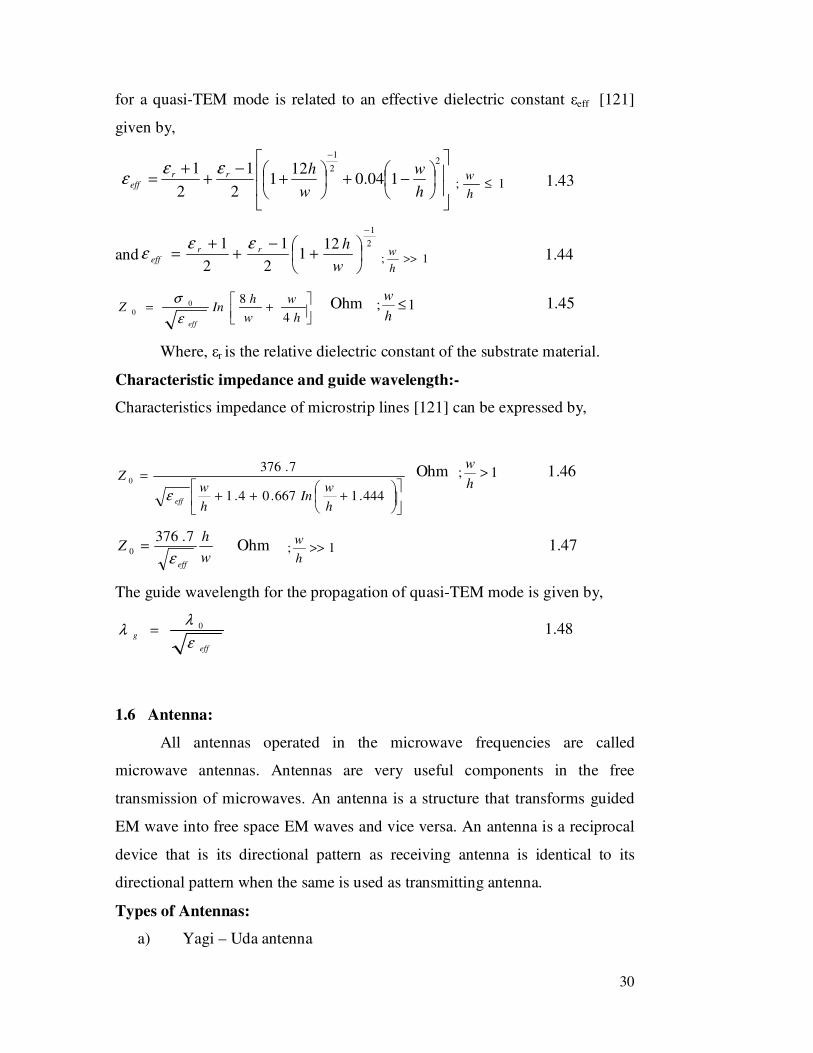
1.6 Antenna:
All antennas operated in the microwave frequencies are called
microwave antennas. Antennas are very useful components in the free
transmission of microwaves. An antenna is a structure that transforms guided
EM wave into free space EM waves and vice versa. An antenna is a reciprocal
device that is its directional pattern as receiving antenna is identical to its
directional pattern when the same is used as transmitting antenna.
Types of Antennas:
a) Yagi – Uda antenna
31
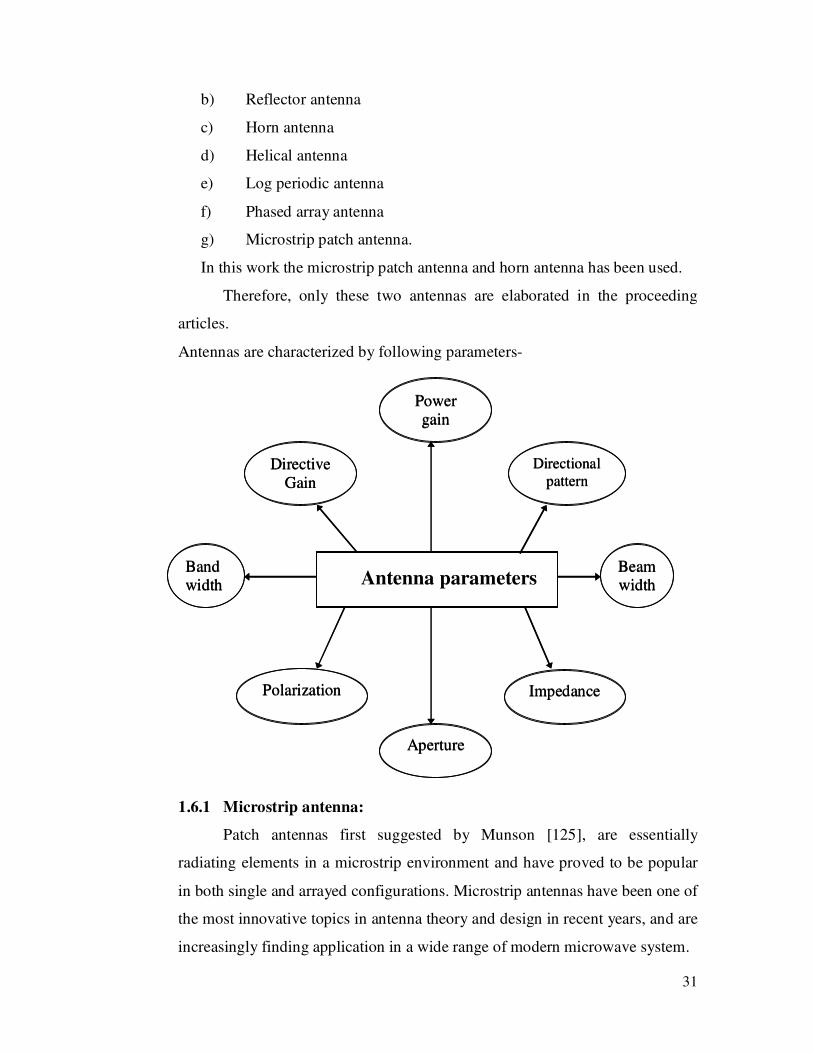
b) Reflector antenna
c) Horn antenna
d) Helical antenna
e) Log periodic antenna
f) Phased array antenna
g) Microstrip patch antenna.
In this work the microstrip patch antenna and horn antenna has been used.
Therefore, only these two antennas are elaborated in the proceeding
articles.
Antennas are characterized by following parameters-
Antenna parameters
1.6.1 Microstrip antenna:
Patch antennas first suggested by Munson [125], are essentially
radiating elements in a microstrip environment and have proved to be popular
in both single and arrayed configurations. Microstrip antennas have been one of
the most innovative topics in antenna theory and design in recent years, and are
increasingly finding application in a wide range of modern microwave system.
Directional
pattern gain
Polarization
Beam
width
gain
Impedance
Aperture
Band
width
Power
gain
Directive
Gain
Directional
pattern gain
Polarization
Beam
width
gain
Impedance
Aperture
Band
width
Power
gain
Directive
Gain
32
The simple configuration of microstrip antenna is a metallic
radiator on a dielectic substrate as a support, with ground plane on the other
side. The metal used is normally gold, copper or silver. Ideally the dielectric
constant of the substrate should be low (εr =2.5), so as to enhance the fringing
fields, which account for radiation. The higher limit for value of εr is 13.
Various types of substrates used are quartz, glass, sapphires, alumina etc.
Alumina (Al2O3) is most commonly used because of higher thermal
conductivity, strength and stability and good electrical properties.
They are used in various systems such as radar, satellite,
communication, missiles, space vehicles and various defense equipments
because of their thin profile, low weight, planar configuration and easy
integrability with other circuits.
Microstrip antennas may be of any geometrical shape and any
dimensions. However all the microstrip antennas may be divided into three
basic categories are:
A) Microstrip patch antennas
B) Microstrip traveling wave antennas
C) Microstrip slot antennas
1.6.2 Equilateral Triangular Microstrip Patch Antenna:
Among the various shapes of the microstrip patch antennas the
rectangular, square, circular and annular ring have been studied extensively. In
contrast, the triangular patch has been the subject of only a handful of
investigations [126-129].
The basic triangular element can be thought of a half wavelength, open
circuited patch fed by either a microstripline in the same plane, or by a coaxial
probe entering under the patch in a perpendicular plane. The equilateral
triangular patch has also received attention due to its interesting features
[130,131]. An experimental study of this antenna was reported by Gang et al
[132]. Equilateral triangular patch antennas have a smaller size compared to
square or circular patch antennas for a given frequency [133-139].
33
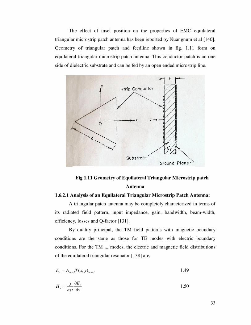
The effect of inset position on the properties of EMC equilateral
triangular microstrip patch antenna has been reported by Nuangnum et al [140].
Geometry of triangular patch and feedline shown in fig. 1.11 form on
equilateral triangular microstrip patch antenna. This conductor patch is an one
side of dielectric substrate and can be fed by an open ended microstrip line.
Fig 1.11 Geometry of Equilateral Triangular Microstrip patch
Antenna
1.6.2.1 Analysis of an Equilateral Triangular Microstrip Patch Antenna:
A triangular patch antenna may be completely characterized in terms of
its radiated field pattern, input impedance, gain, bandwidth, beam-width,
efficiency, losses and Q-factor [131].
By duality principal, the TM field patterns with magnetic boundary
conditions are the same as those for TE modes with electric boundary
conditions. For the TM mn modes, the electric and magnetic field distributions
of the equilateral triangular resonator [138] are,
lnmlnmz yxTAE ,,,, ),(= 1.49
y
EjH z
x∂
∂=
ωµ 1.50
34
x
EjH y
∂
∂−=
ωµ 1.51
0=== yxz EEH 1.52
where,
( ) ( )
( )53.1
3
)(2cos
3
2
3
2cos
3
2cos
3
2
3
2cos
3
2cos
3
2
3
2cos),(
,,
−−−−−−−−−−−−−−−−−−−
−Π
Π+
Π+
−Π
Π+
Π+
−Π
Π+
Π=
a
ymln
a
x
a
ylnm
a
x
a
ynml
a
xyxT
lnm
And A m,n,l is an arbitrarily amplitude constant, a is the length of a side of the
triangle, and m,n,l are integers which are never zero simultaneously and which
satisfy the condition,
0=++ lnm 1.54
The fields satisfy the wave equation
02
22
2
=
+
∂
∂+
∂
∂zmn EK
yx 1.55
where,
22
3
4nmnm
aKmn ++
Π= 1.56
It is observed that interchanging the three digits m, n, l leaves the wave number
K mn and the field patterns unchanged. The field patterns for the first two
modes.
The above expressions for the fields are general. The particular case, m = 1 ,
n=0 and l = -1 corresponds to the dominant mode, for which the field
expressions are,
Π+
Π
Π+
Π= −
a
y
a
y
a
xAE z
3
4cos
3
2cos
3
2
3
2cos21,0,1
1.57
Π+
Π
Π+
Π−= −
a
y
a
y
a
xjAH x
3
4sin
3
2sin
3
2
3
2cos01,0,1 ξ 1.58
Π
Π+
Π= −
a
y
a
xAjH y
3
2cos
3
2
3
2sin3 01,0,1 ξ 1.59
)(120
10 mhos
Π=ξ
35
1.6.2.2 Resonant frequency:
The resonant frequency of the equilateral triangular patch [136] can be
calculated by using,
21
22 )(3
2
2nmnm
a
cckf
rr
mn
r ++=Π
=εε
1.60
where,
c is the velocity of the light (3×10¹⁰
cm/s) in free space.
a = length of equilateral patch
εr = relative permittivity of dielectric substrate
A plot of the product (fr × a) as a function of εr for various values of m and n.
The lowest order resonance frequency is,
r
ra
cf
ε3
2= 1.61
This relationship does not take into consideration end effects or effects of
fringing fields. The resonant frequency may be determined with better accuracy
if єr is replaced by effective dielectric constant which may be calculated from
the average values of the effective dielectric constants for strip width’s W=0
and w=A.
2/1.121
4
1
2
1 −
+
−+
+=
a
hrr
e
εεε 1.62
Similarly the end effects are taken into account by replacing a by aeff an
approximate value of aeff is given by,
r
effhaa
ε+= 1.63
Thus, the final expression for the lowest order resonant frequency becomes,
eeff
r
a
cf
ε3
2= 1.64
The frequency difference between theoretical values and experimental results is
approximately 3%. For high dielectric constant substrates such as alumina, εr
should be used in place of εe.
36
1.6.2.3 Radiation fields:
The triangular patch was first introduced by Helszajn and James [139] as
a traveling wave antenna. Its resonant behavior was studied by Mink [141]. The
equilateral triangular patch is used as resonator.
The radiation characteristics of two-element array of equilateral
triangular patch antenna are theoretically studied in presence of EM waves. The
radiation fields of an equilateral triangular patch antenna may be obtained by
calculating the vector electric potential [129].
The far field components may be calculated from
Er=0
[ ]φφωηθ cossin0 yx FFjE +−−= ---- 1.65
[ ]φθφθωηφ sincoscoscos0 yx FFjE += ---- 1.66
The expression for the total radiation field pattern R (θ,φ) is obtained as,
( )22
, tt EER φθφθ += ---- 1.67
Then, the radiation field patterns in the E plane (φ = 0) and the H plane
(φ = π/2) are given as,
(E-Plane) --- 1.68
(H-Plane) ---- 1.69
The triangular patch antenna is characterized by a single parameter namely the
length of patch.
1.6.3 Horn antenna:
In this work horn antenna is used as receiving antenna. A horn antenna
may be regarded as a flared out (or opened-out) waveguide. The function of the
horn is to produce a uniform phase front with a larger aperture than that of the
waveguide, and hence greater directivity.
Several types of Horn antennas [142, 143] are illustrated in figure 1.12
( )θωη 2222
0
2
0 cosXyE FFR +=
( )θωηφθ 2222
0
2
0 cos),( yxH FFR +=
37
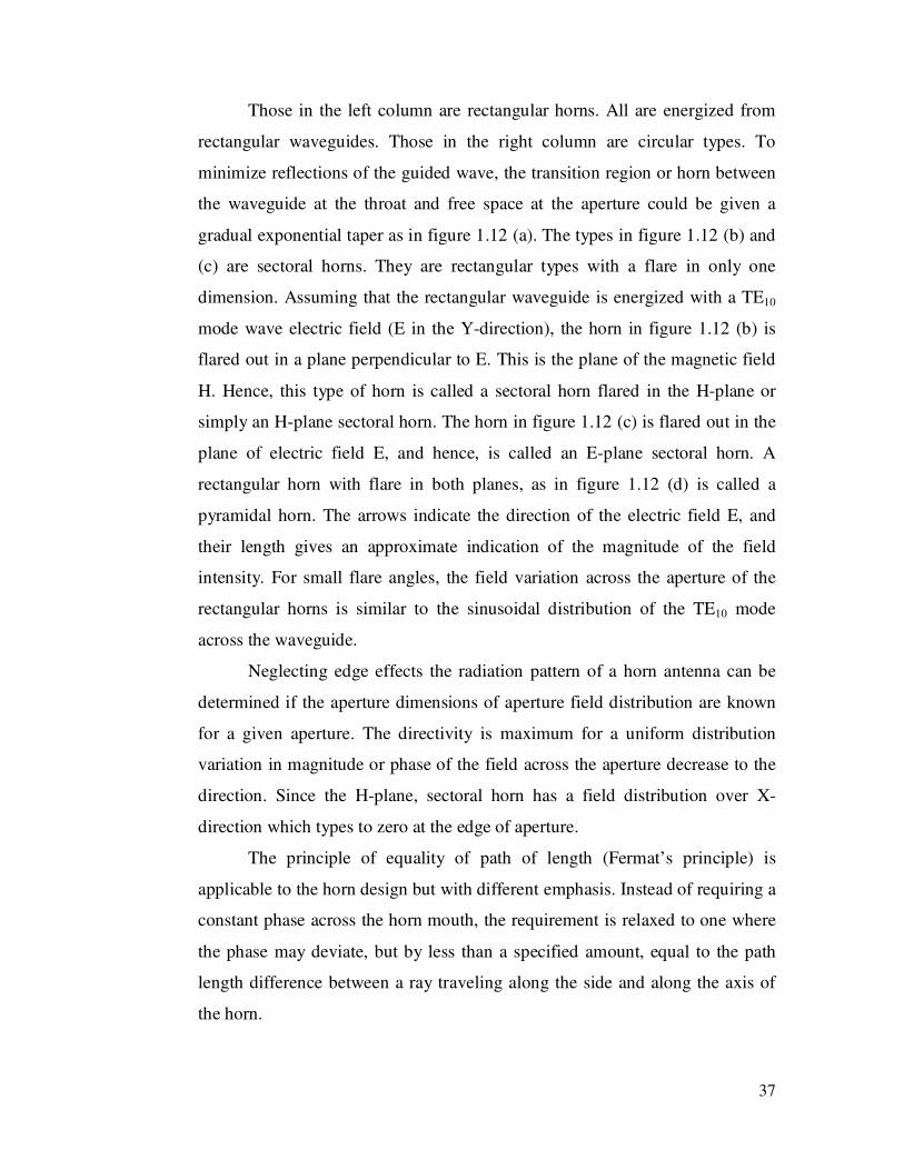
Those in the left column are rectangular horns. All are energized from
rectangular waveguides. Those in the right column are circular types. To
minimize reflections of the guided wave, the transition region or horn between
the waveguide at the throat and free space at the aperture could be given a
gradual exponential taper as in figure 1.12 (a). The types in figure 1.12 (b) and
(c) are sectoral horns. They are rectangular types with a flare in only one
dimension. Assuming that the rectangular waveguide is energized with a TE10
mode wave electric field (E in the Y-direction), the horn in figure 1.12 (b) is
flared out in a plane perpendicular to E. This is the plane of the magnetic field
H. Hence, this type of horn is called a sectoral horn flared in the H-plane or
simply an H-plane sectoral horn. The horn in figure 1.12 (c) is flared out in the
plane of electric field E, and hence, is called an E-plane sectoral horn. A
rectangular horn with flare in both planes, as in figure 1.12 (d) is called a
pyramidal horn. The arrows indicate the direction of the electric field E, and
their length gives an approximate indication of the magnitude of the field
intensity. For small flare angles, the field variation across the aperture of the
rectangular horns is similar to the sinusoidal distribution of the TE10 mode
across the waveguide.
Neglecting edge effects the radiation pattern of a horn antenna can be
determined if the aperture dimensions of aperture field distribution are known
for a given aperture. The directivity is maximum for a uniform distribution
variation in magnitude or phase of the field across the aperture decrease to the
direction. Since the H-plane, sectoral horn has a field distribution over X-
direction which types to zero at the edge of aperture.
The principle of equality of path of length (Fermat’s principle) is
applicable to the horn design but with different emphasis. Instead of requiring a
constant phase across the horn mouth, the requirement is relaxed to one where
the phase may deviate, but by less than a specified amount, equal to the path
length difference between a ray traveling along the side and along the axis of
the horn.
38
Fig 1.12 Types of rectangular and circular horn antenna
(Arrows indicate E field direction)
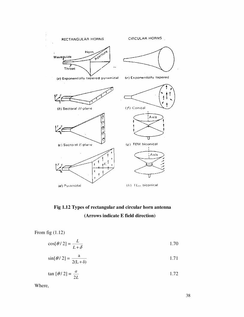
From fig (1.12)
cos[θ / 2] = δ+L
L 1.70
sin[θ / 2] = δ)2(L
a
+ 1.71
tan [θ / 2] = L
a
2 1.72
Where,
39
θ = Flare angle (θE for E-plane, θH for H-plane)
a = Aperture (aE for E-plane, aH for H-plane)
L = Horn length.
From the geometry, we have also that,
L =δ8
2a
, δ<<L 1.73
And θ = 2tan-1δL
L2cos
2L
a 1
+= − 1.74
In the E plane of the horn, δ is usually held to 0.25 λ or less. However, in the H
plane, δ can be larger, or about 0.4 λ, since E plane goes to zero at the horn
edges.
The optimum horn dimension can be related by,
δ0 = )2/cos(θ
L - L 1.75
Where, L = )2/cos(1
)2/cos(0
θ
θδ
− 1.76
It follows that the width of the waveguide at the throat of the horn must be
between λ/2 and λ, or if the excitation system is symmetrical, so that even
modes are nor energized, the width must be between λ/2 and 3λ/2.
1.6.3.1 Radiation pattern:
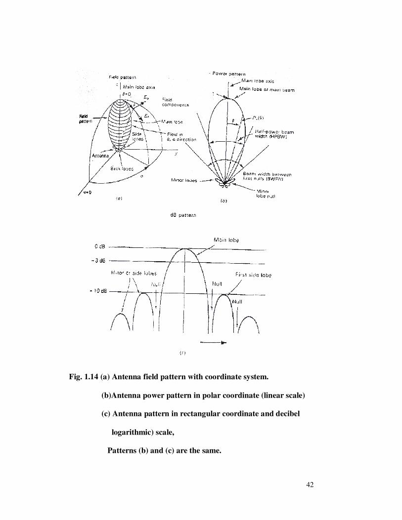
An antenna radiation pattern is defined as a graphical representation of
the radiation properties of the antenna as a function of space coordinates. The
radiation pattern can be of various types:
i) Isotropic
ii) Omni directional
iii) Pencil beam
iv) Fan beam
v) Shaped beam
40
Fig. 1.13 (a) Pyramidal horn antenna.
Fig. 1.13 (b) Cross section with dimensions in analysis.
The diagram can be for either E plane or H plane cross section. For the E
plane, the flare angle is θθθθE and aperture aE (For the H plane the flare angle
is θθθθH and the aperture aH)
Various parts of the radiation pattern are called lobes –
a) Major lobe
b) Side lobe
c) Back lobe
d) Minor lobe
A major lobe (main lobe) is defined as the radiation lobe containing the
direction of maximum radiation.
A side lobe is a radiation lobe in any direction other than the main lobe.
A back lobe usually refers to a minor lobe that occupied the hemisphere
in a direction opposite to that of major lobe.
41
Minor lobe usually represents radiation in undesired direction and they
should be minimized.
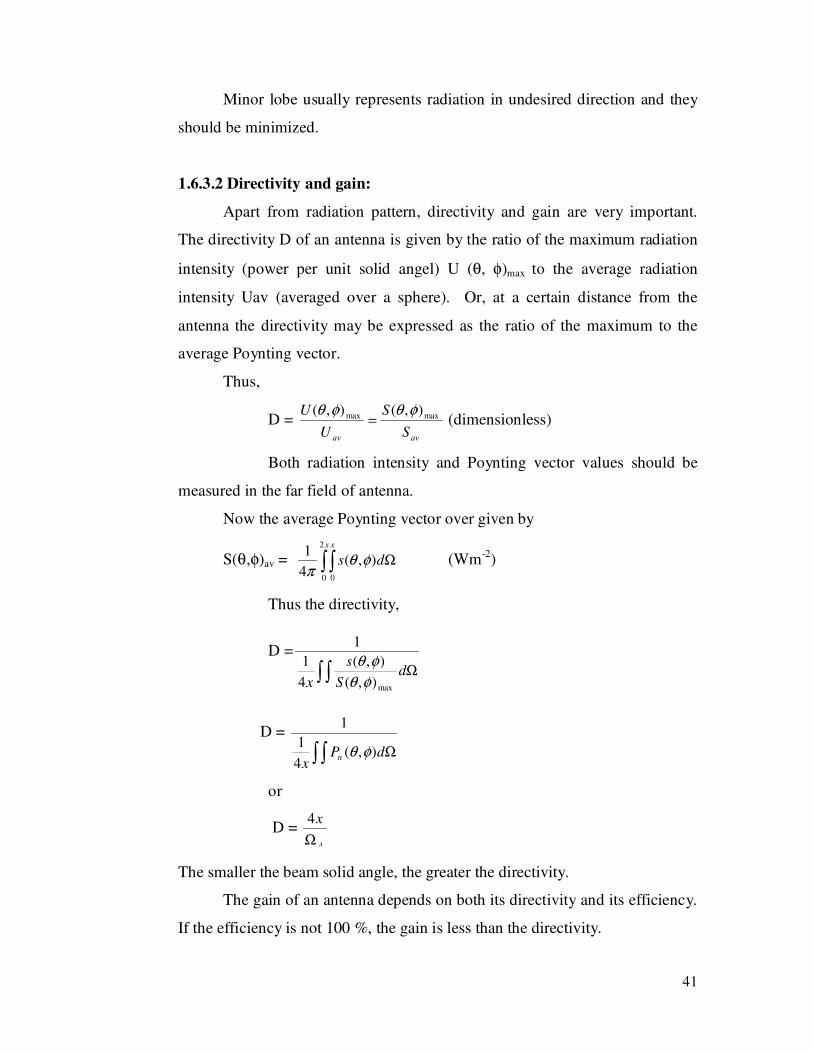
1.6.3.2 Directivity and gain:
Apart from radiation pattern, directivity and gain are very important.
The directivity D of an antenna is given by the ratio of the maximum radiation
intensity (power per unit solid angel) U (θ, φ)max to the average radiation
intensity Uav (averaged over a sphere). Or, at a certain distance from the
antenna the directivity may be expressed as the ratio of the maximum to the
average Poynting vector.
Thus,
D = avav S
S
U
U maxmax ),(),( φθφθ= (dimensionless)
Both radiation intensity and Poynting vector values should be
measured in the far field of antenna.
Now the average Poynting vector over given by
S(θ,φ)av = ∫ ∫ Ωx x
ds
2
0 0
),(4
1φθ
π (Wm-2)
Thus the directivity,
D =
∫ ∫ ΩdS
s
x max),(
),(
4
1
1
φθ
φθ
D =
∫ ∫ ΩdPx
n ),(4
1
1
φθ
or
D = A
x
Ω
4
The smaller the beam solid angle, the greater the directivity.
The gain of an antenna depends on both its directivity and its efficiency.
If the efficiency is not 100 %, the gain is less than the directivity.
42
Fig. 1.14 (a) Antenna field pattern with coordinate system.
(b)Antenna power pattern in polar coordinate (linear scale)
(c) Antenna pattern in rectangular coordinate and decibel
logarithmic) scale,
Patterns (b) and (c) are the same.
43
Thus the gain,
G=kD (dimensionless)
Where, k = efficiency factor of antenna (0 ≤ k ≤ 1), dimensionless.
1.7 Fabrication of the Microstrip components:
There are two types of hybrid technologies involved for the
fabrication of hybrid microwave circuits.
1) Thick film technology
2) Thin film technology.
H. Sobol [144] has reported that the term thin film or thick film refers to the
process used and not to the thickness of the film.
Thick films are realized by the process of screen printing of an
appropriate type of paste or ink on the substrate and are fired at the specified
temperature. Depending upon the composition of the inks, after firing they
give rise to conductors, resistors or dielectrics. Basically, there are six
techniques for fabrication of microstripline circuits [145].
These are
1. Vacuum deposition.
a. Evaporation through mask (additive process).
b. Evaporate allover and photo etch (subtractive process).
2. Dc sputter allover and photo etch.
3. Dc sputtering followed by electroplating and photo etch.
4. Vacuum deposition followed by electroplating and photo etch.
5. Electro-less deposition followed by electroplating and photo etch.
6. Screen print and fire i.e. thick film technology.
a. Pattern screened directly.
b. Pattern photo etched from screened and fired inks.
In the present work only screen printing (thick film technology) was
used for microstrip circuit fabrication, so only this technique is discussed in
brief in the following article.
44
1.7.1 Thick film Deposition Technique:
The features and potential of thick film technology has made it one of
the leading solid-state technologies. This section reviews the thick film process
used for fabricating our thick films. The history of thick film technology dates
back to 1950’s. It soon became clear that the result of fabricating components
with different technologies could open up a whole new field in electronics.
Now a days thick film technology is widely, used technology for gas sensors
fabrication.
A thick film circuit is basically considered to consist of a layer of
special inks or pastes deposited on to an insulating substrate. By adding
integrated circuits, and sometimes film made by other techniques, a hybrid
circuit is produced. One of the key factor that distinguishes a thick film, is the
method of film deposition screen-printing, which is possibly one of the oldest
form of graphic art reproduction.
The term thick film has gained acceptance as the preferred generic
description for that field of microelectronics in which specially formulated
pastes are applied and fired onto a ceramic substrate in a definite pattern and
sequence to produce a set of individual components, such as resistors and
capacitors, or a completely functional circuit [146-148].
The deposition process adopted for thick film production is similar to that used
in traditional silkscreen printing of pencils, mugs, visiting cards etc. The degree
of sophistication of the printing, and the nature of the screen materials, are
somewhat different for the microelectronics circuit production requirements. A
typical thick film screen is made from a finely woven mesh of stainless steel,
polyester or nylon. This is mounted under tension on a metal or wooden frame
and coated with an ultraviolet sensitive emulsion upon which the circuit pattern
could be formed photographically. The finished screen has open-mesh areas
through which the desired pattern can be printed. The screen is held in a
position within screen-printing machine at a distance around 0.5mm from the
surface of the substrate. The thick film paste, which is resistive, conductive or
dielectric in nature, is placed on to the top surface of the stencil and a squeegee
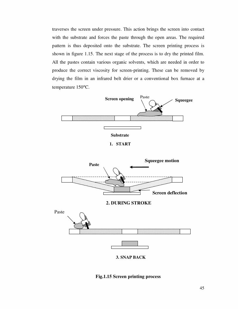
45
Paste
3. SNAP BACK
Screen deflection
Squeegee motion Paste
2. DURING STROKE
Paste Squeegee Screen opening
Substrate
1. START
traverses the screen under pressure. This action brings the screen into contact
with the substrate and forces the paste through the open areas. The required
pattern is thus deposited onto the substrate. The screen printing process is
shown in figure 1.15. The next stage of the process is to dry the printed film.
All the pastes contain various organic solvents, which are needed in order to
produce the correct viscosity for screen-printing. These can be removed by
drying the film in an infrared belt drier or a conventional box furnace at a
temperature 150°C.
Fig.1.15 Screen printing process
46
After drying, the films retain a rigid pattern on the substrate and are
relatively immune to smudging. In certain circumstances, another layer can be
printed directly onto a dry film, but more often, the next step in the process is
to fire the film at high temperatures. In addition to the organic vehicle, thick
film pastes also contain finely divided particles of active material having an
average diameter around five microns, and a frit (powdered glass) or some
metal oxide having low melting point which act as binder. During the firing
(annealing) process the glass melts, the fine powder sinters and the overall film
becomes a solid composite material.
The function of the glass (metal oxide) is to bond the film to the
substrate and also to bind the active particles together. Firing is performed in a
belt furnace at peak temperature around 850°C (or in a Muffle furnace with
controlled heating rate). After firing the film is firmly attached to the substrate.
The thick film pastes used in this work are fritless (does not containing glass).
1.8 Microstripline components with overlay: A brief survey
In this work moisture dependent different types of oil seeds are used as
overlay over simple microstripline and microstrip patch antenna. When any
material is kept in contact with microstrip components over it is termed as
overlay or superstrate. When the overlay is used over a open microstripline, it
is called Multilayer Microstrip [149].
The overlay effects due to fringing field of microstrips are mainly
governed by the dielectric constant (εr) [150, 151] of the overlay e.g. (a) with
increase in the (εr) of the overlay, the fringing field lines get concentrated, thus
increasing the fringing field capacitance, which finally results decrease in
resonance frequency fr of the resonator [152]. (b) When metallic overlay is
used with dielectric spacing (d), as a result of induced charges in the metal, the
fringing fields, capacitance of the microstrip decreases which results in
increase in fr. (c) At the same time it is observed that very large and/or very
small (εr) of the overlay are not much effective in changing the fr [153]. Mesa
[154] has studied the leakage from microstripline due to overlay. A leaky
47
dominant mode can exist on microstripline without top cover, but only for
relatively high frequency or thick substrates. However when top cover is
introduced over the substrate, the frequency at which leakage begins is
dramatically lowered.
The conductive patches of microstrip antennas are often covered by a
dielectric layer for protective purpose or for other mechanical / Thermal
requirements. In many of the practical design, this cover layer is electrically
much thicker than the substrate thickness and can adversely affect the antenna
basic radiation characteristics.
It has been found that [155], the bandwidth of the radiation pattern in the
E plane will initially decrease and then increase upon increasing normalized
thickness of the cover. It was found [156] that the antenna directivity can be
changed by adjusting the loading of dielectric resonator core or by varying the
permittivity of dielectric resonator material. The effect of coupling on various
parameters of the microstrip antenna, and consequently effect of inter elements
spacing with different dielectric materials placed in between the patches have
been investigated [157, 158].
The effect of angle dependant perturbation of circular patch antenna due
to alumina strips as overlay has been reported by Nuangnum et al [140]. Dual
band microstrip antennas have been achieved by means of loading by shorting
pins [159,160], crossed slot [161]. The influence of complex material covering
on the quality factor of the antennas has been investigated by Tretyakov et al
[162]. Multilayer microstrip antennas have been analyzed by workers [163,
164].
Most of the experimental data on overlay on thick film microstrip
component in existence is from our lab [113-118,165-174] where dielectric
overlays in bulk, thin film and thick film form has been studied on both thin
film and thick film microstrip components. The work on thin film ring
resonator as moisture sensor in X band has also been reported [108-110]. To
the authors knowledge, the effect of the seeds on non resonant miniaturized Ag
48
thick film microstripline and resonant equilateral triangular patch antenna in
the Ku band has not been studied by any worker.
1.9 Aim of the work:
The microstrip component being in planar form can offer an alternative
miniaturized device for granular materials of uneven shape and size like oil
seeds and cereal grains. The work in our lab has shown that thick film
technology is cost effective and compatible for fabrication of microstrip
components in the frequency range 8 - 18 GHz [175-178]. Resonant and non-
resonant circuits are very useful in numerous applications in the microwave
field. There are very few studies on the Ag thick film microstripline and
equilateral triangular microstrip patch antenna upto 18 GHz.
To the authors knowledge using Ag thick film simple microstripline the
dielectric characterization and prediction of moisture content of seeds has been
reported for the first time in this work. The waveguide reflectometer and
VSWR slotted section method has also been studies for the seeds for the first
time. From the response of the various microstrip components, the microwave
permittivity, conductivity, prediction of moisture content of seeds has been
done here.
The thesis deals broadly with four aspects.
1. Design, fabrication and characterization of Ag thick film microstripline
and equilateral triangular microstrip patch antenna in the Ku band.
2. Use of non-resonant simple microstripline to characterize the three
different types of oil seeds by overlay technique and predict the moisture
content percentage.
3. Use of resonant circuit equilateral triangular microstrip patch antenna to
characterize the three different types of oil seeds by overlay technique
and predict the moisture content (%).
4. The waveguide reflectometer and VSWR slotted line technique has also
been used for the study of microwave dielectric properties and moisture
content prediction.
49
In this work, an attempt has been made to study the dielectric properties
of the moisture laden seeds and electrical parameters such as transmission,
reflection, resonance frequency, bandwidth, and Q-factor through the Ag thick
film microstripline circuits.
Three types of seeds were used for study in this work. All these seeds
grown in Krishna Valley at Sangli district in Maharashtra state of India (June-
Sept 2006) were selected. It has been used as overlay over two types of
microstripline components viz. Ag thick film microstripline and Ag thick film
equilateral triangular patch antenna. The seed was used as in touch overlay.
Due to small seed size only partial overlay has been done.
The microwave dielectric properties and prediction of moisture content
from overlay method have been compared with those obtained by waveguide
reflectometer method and VSWR slotted line method.
The thesis is divided into six chapters. Chapter-I includes the relevant
literature survey and theoretical considerations of microstrip components. The
range of microwave frequency is also useful for agricultural purposes given.
Various techniques has been explained. The experimental method used has
been elaborated in Chapter-II. The data obtained from the experiments carried
out by overlay technique using Ag thick film microstripline has been explained
in the form of graphs and tables in Chapter-III. The dielectric characterization
and prediction of moisture content are also elaborated here.
The data obtained from overlay studies using Ag thick film equilateral
triangular patch antenna for the dielectric characterization and moisture
prediction has been explained in chapter-IV. Chapter-V gives the results
obtained by waveguide reflectometer and VSWR slotted section method for
seeds. The discussion of the results of the studies of soybean, sunflower and
groundnuts using microstrip components and waveguide techniques elaborated
in chapter-VI. The summary and conclusions are also given in this Chapter.
50
REFERENCES
1. W. Schilz, B.Schiek : Advances in Electronics & Electron Physics,
Vol.55, pp. 309-381,(1981).
2. M. A. Stuchly, S.S. Stuchly: IEEE Proc. Vol.130, pp.467-503, (1983).
3. S.O. Nelson: Trans ASAE, Vol. 30, No.3, pp.818-831, (1987).
4. A.W. Kraszewski: IEEE Trans. On Microwave Theory & Tech. MTT-
39, No. 5, pp. 828-835, (1991).
5. S. Trabelsi, S.O. Nelson: Meas. Sci. Technol., Vol. 14, pp.589-600,
(2003).
6. S. Rane, V. Puri: Microelectronics Journal, Vol. 32, pp. 649-654,
(2001).
7. S. Rane, V. Puri: Microelectronics Reliability, Vol. 42, pp. 1953-1958,
(2002).
8. A.W. Kraszewski, S.O.Nelson: Journal of Microw. Power Em. Energy,
Vol.38, pp.13-35, (2003).
9. J. Sheen: Meas. Sci. Technol, Vol.20, pp.1-12, (2009).
10. V. N. Egorov: Instrum. Exp. Tech, Vol. 50, pp.143-175, (2007).
11. J. M. C. Civeca, A.J. canos, F.L.P.Forx, E.De Losr Davo: IEEE
Trans Microw. Theo. Tech. Vol.51, pp. 16-14, (2003).
12. Y.Hayashi, G.Nishima, K. Hirayama, Y.Hayashi: Electron.
Commun. Japan Part II. Electronics, Vol 86, pp. 32-41, (2003).
13. J.Baker-Javis, E.J.vanzeua, W.A. kirsick: IEEE Trans. Microw.
Theo. Tech. Vol.38, pp. 1096-1103, (1990).
14. S. A. Jamadade, V. Puri: Applied Surface Sci., Vol. 255, pp.4201-
4204, (2009).
15. J. Meachen, A. Duffy, J. William, C.H.Oxley: Microw.
opt.Technol.Lett. Vol.51, No. 6, pp.1416-1419, (June,2009).
16. J. Sheen: IEEE Trans. Dielectr. Electr. Instrl. Vol.14, pp.1139-1144,
(2007).
17. J. Sheen: J.Appl. Phys., Vol.102, 014102, (2007).
51
18. T.Kanai. T.Tsukamoto, M. Miyakawa, T. Kashiwa: IEEE Trans
Magn, Vol.36, pp.1750-1753, (2000).
19. A.Kaczkowshi, A.Milewshi: IEEE Trans. Microw. Theo. Tech.
Vol.28, pp. 225-228, (1980).
20. J.Sheen: Measurement, Vol.37, pp.123-130, (2005).
21. B.W.hakki-P.d.Coleman: IRE Trans Microw. Theor. Tech.Vol. 8,
pp.402-410, (1960).
22. Stephen F. Adam: Microwave Throry and application, Hewlett
Packard Company, (1969).
23. D. K. Ghodgaonkar, V. V. Vardan, V. K. Vardan: IEEE Trans
Instrum. Meas. Vol.38, pp.789-793, (1989).
24. J. Musil, F.Zack: Microwave measurement of complex permittivity
by free space methods and applications, new York Elsevier, (1986).
25. V.K.Varadan: Microw. Opt. Technol. Lett., Vol.26, No. 2, pp. 100-
105, (July,2000).
26. A.W. Kraszewski, S. Trabelsi, S.O. Nelson: J. MW. Power and EM
energy, Vol. 37(1), pp. 41-54, (2002).
27. D.C.Kulkarni, U.B. Lonkar and V.Puri: J.M.M.M., Vol.320,
pp.1848-1853, (2008).
28. S.V. Jadhav, V.Puri: Microelect. Journal, Vol.39, pp.1475-1478,
(2008).
29. R. G. S. Sophin, R.C.Aiyer: Microw. Opt. Technol. Lett., Vol.47, No.
1, pp. 11-14, (Oct,2005).
30. Z.Wang, W.Che, Y.Chang: Microw. Opt. Technol. Lett., Vol.50, No.
7, pp. 1800-1804, (July,2008).
31. S.Hadjiloucas, L.S.Kanatzas, J.W. Brown: IEEE Trans. Microw.
Theo. Tech. Vol.47, No.2 pp. 142-149, (1999).
32. R. M.Nanayanan, K.T.Vu: J.Food Progress Pre- seevation, Vol.24,
pp. 39-56, (2000).
33. Z. Ma, S. Okamura: J. Microw. Power Electromag. energy, Vol.33,
pp.178-183, (1998).
52
34. ASAE, St. Joseph, ASAE Standards 1995: ASAE S 352.2, (1995).
35. J. C. Multon: Int Assoc of cereai Chemistry Vienna, Austria, (1976).
36. Int. Standard: ISO 76, (1978).
37. D.C. Zimmerman: J. Am. oil Chem Soc. Vol. 53, No. 8, pp.548-550,
(Aug, 1976).
38. Resonance System Ltd., Information brochure, http://
www.mobilenmr.com, (2005).
39. K.J. Kaffka, K.H.Norris, J.Peredi, A. Balagh: Acta alimentania, Vol.
11, No. 3, pp.253-269, (1982).
40. I. Ben Gera, K.H. Norris: J. Agric Res., Vol.18, pp. 125-132, (1968).
41. J. A. Robertson, F.E. Barton: J. Am. Oil Chem. Soc. Vol. 61, No. 3,
pp.543-547, (1984).
42. R.A. Hartwig, C.R. Hurbugh: J. Am. Oil Chem. Soc. Vol. 67, No. 7,
pp.682-686, (1990).
43. P.C. William, D.C.Sobening: J. Near IR Spectrosc., Vol. 1, pp.25-32,
(1993).
44. S. Trabelsi, S.O. Nelson ,A.W. Kraszewski: Proc.of 19th IEEE Trans.
Instr. and Meas. tech., Vol. 2, pp-1381-1385 (2002).
45. S. Trabelsi, A.W. Kraszewski, S.O. Nelson: IEEE Trans. Instrum.
Meas. Vol.47, pp. 127-132, (1998).
46. R. Jacobsen, W.Meyer, B. Schrage : 10th
European Microwave
Conf., Warsaw, Poland. pp. 216-220, ( 1980).
47. M. Kent, W. Meyer: J. of Food Eng. Vol.1, pp. 31-42, (1982).
48. E. Kress- Rogers, M Kent: J. of Food Eng. Vol.6, pp. 345-376,
(1987).
49. A. Kraszewski: J. of Microwave power, Vol.23, pp. 236-246, (1988).
50. S. Trabelsi, S.O. Nelson: Meas. Sci. Technol , Vol. 9, pp.570-578,
(1998).
51. S. Trabelsi, A.W. Kraszewski, S.O. Nelson: J. of Agric. Eng. Res.
Vol. 71, pp.227-237, (1998).
52. J.B.Hasted, Aqueous Dielectric, (Chapman and Hall, London), (1973).
53
53. A. Kraszewski, S. Trabelsi, S.O. Nelson: IEEE Trans. Instrum.
Meas. Vol.50, pp. 877-881, (2001).
54. R. Jacobsen, W. Meyer, B. Schrage: 10th European microwave
conference, Warsaw, Poland, (1980).
55. W. Meyer, W. Schlitz: J. Appl. Phys., Vol. 13, pp. 1823-1830, (1980).
56. W. Meyer, W. Schlitz: IEEE Trans. Microw. Theory Tech., Vol. 29,
No. 7, pp. 732-739, (1981).
57. M. Kent, W. Meyer: J. Food Eng., vol. 1, no. 1, pp. 31-42, (1982.)
58. F. Menke, R. Knochel: IEEE MTT-S Symposium, San Francisco,
(1996).
59. S. Trabelsi, A. Kraszewski, S.O. Nelson: IEEE Trans. Inst. Meas.,
Vol. 47, No. 3, pp. 613- 622, (1998).
60. S. Trabelsi, S.O. Nelson, Meas. Sci. Tech., Vol. 9, pp. 570-578,
(1998).
61. D.D. Archibald: Appl. Spectro, Vol. 52, No. 11, pp. 1435-1446,
(1998).
62. P.G. Bartley Jr. et al: IEEE Trans. Inst. Meas., Vol. 47, No. 2, pp.
123-125, (1998).
63. Y. Zheng, S. Okamura: IEEE Trans. Inst. Meas., Vol. 48, No. 6, pp.
1208-1211, (1999).
64. F. Volgyi, J. Burrows, R. Shepherdson: 4th International symposium
on humidity and moisture sensors ISHM’02, Taipei, Taiwan, (2002).
65. K. Kupfer, in Electromagnetic aquametry: (Springer-Verlag, Berlin
Heidelberg, , pp. 135-167, (2005).
66. S.Trabelsi, S.O. Nelson, M.A.Lewis: Sens. & Instrumen. Food Qual.
Vol.3, pp.114-121, (2009).
67. S.Trabelsi, S.O. Nelson: Meas. Sci. Technol. Vol.18, pp.997-1003,
(2007).
68. P.Meszaros, D.B.Funk: Prog.in Agri. Engg. Sci. Vol.2, pp.73-94,
(2006).
54
69. C.V.K. Kandala, S. O. Nelson: Meas. Sci. Technol, Vol. 18, pp.991-
996, (2007).
70. S. Trabelsi and S. O. Nelson: IEEE Trans. Instrum. Meas., Vol. 56,
No. 1 pp. 194–198, (2007).
71. S. Trabelsi, S. O. Nelson: IEEE Trans. Instrum. Meas., Vol. 55, No.
3, pp. 953–963, (2006).
72. S. Trabelsi, S. O. Nelson: Presented 22nd IEEE Instrum. Meas.
Technol. Conf., (2005).
73. S. Trabelsi , S. Nelson: Trans. ASAE, Vol. 47, pp. 1999–2008,
(2004).
74. S. Trabelsi, S.O. Nelson: Trans. Of ASAE Annual International
meeting, pp.1-15, (2003).
75. S. Trabelsi, A.W. Kraszewski, S.O. Nelson: Electronic Lett. , Vol.
35, No.16, pp.1346-1347, (1999).
76. A. W. Kraszewski: Surface sensing Technologies and Application,
Vol.2, No.4, pp. 347-362, (2001).
77. S. Trabelsi, A.W. Kraszewski, S.O. Nelson: Trans. ASAE, Vol. 44,
No.33, pp.731-736, (2001).
78. S. Trabelsi, A.W. Kraszewski, S.O. Nelson: Trans. of ASAE,
Vol.42, No.2, pp. 531-536, (1999).
79. A.W. Kraszewski, S.O. Nelson: J. MW. Power and EM energy, Vol.
39, No.1, pp. 41-52, (2004).
80. S.O. Nelson, P. G. Bartley: Trans. ASAE, Vol. 45, No.4, pp. 1223-
1227, (2002).
81. S. Trabelsi, A.W. Kraszewski, S.O. Nelson: Meas. Sci. and
Technol, Vol. 12, pp 2192-2197 (2001).
82. S.O. Nelson, A.W. Kraszewski, S. Trabelsi, K. C. Lawrence: IEEE
Trans. Instrum. Meas. Vol. 49, No.3, pp.470-475, (2000).
83. A.W. Kraszewski, S. Trabelsi, S.O. Nelson: Meas. Sci. Technol.
Vol.8, pp. 857-863, (1997).
55
84. S.O. Nelson, A.W. Kraszewski, S. Trabelsi: IEEE Inst. and Meas.
Tech. Conf. Proc., Vol. 17, pp. 237-247, (1999).
85. J.H. Kim, K.B. Kim. S.H. Noh: Journal of Electrical Engineering And
Information science, Vol. 2, No. 4, pp. 72-78, (1997).
86. C.L. Bulls, J.J. Davidson, M.C. Lamb, C.V.K.Kandala,
J.M.froeger: Trans.of ASAP. Vol. 47, pp. 925-932, (2004).
87. M.B. Slima, R.Z. Marawski: IEEE Trans. on instrum. And Meas.,
Vol. 48, No. 3, pp. 778-782, (June 1999).
88. M.A. Zhihong, S. Okamura: IEICE Trans, Vol. 19, pp. 139-143,
(1997).
89. S. Trabelsi, A.W. Kraszewski, S.O. Nelson: US Patent No.6, 691,
pp.563-567, (2004).
90. S. Trabelsi, S.O. Nelson: Int. Conf. on Electro. Wave Inter. Water
and Moist Subst. MFPA, Weimer, Germany K Kupfer, pp. 231-235,
(2005).
91. P.G. Bartley, S.O. Nelson, R.W. Mcclendon, S. Trabelsi : IEEE
Trans. on Instrum. & Measu., Vol. 47, No. 1, pp. 123-125, (Feb. 1998).
92. M.Kent, R. Knochel, F. Dasnner, U.K. Berger: Eur. Food
Res.Technol, Vol. 210, pp. 359-366, (2000).
93. F. Dasnner, R. Knochel: Adv. Radio Sci. Vol. 1, pp. 9-13, (2003).
94. S. Trabelsi, S.O. Nelson: IEEE Trans. Instrum. Meas. Vol. 55, pp.953
963, (2006).
95. S.O. Nelson, A.W. Kraszewski, S. Trabelsi, K. C. Lawrence: IEEE
Trans. Instrum. Meas., Vol. 49, No.1, pp.56-60, (2000).
96. American society of Agricultural Engg.: (ASAE) S352.2:(S.T.
Joseph, MI: ASAE), pp.563,(2000).
97. K.C. Lawrence, S.O. Nelson, P. G. Bartley: ASAE 41, No.1, (1998).
98. S.O. Nelson: IEEE Instrum. Meas. Mag., Vol.3, No.1, pp. 17-20,
(2000).
99. F.T. Ulaby, R. P. Jedlicka: IEEE Trans. on Geoscience and Remote
Sensing, Vol. GE. - 22, No. 4, pp. 406-413, (1984).
56
100. J.Sachs, P.Peyerl; Fourth Inter.con.on EM inter.with water and
moist substances. (2001).
101. Hewlett-Packard CO: Hewlett-Packard CO., (1993)
102. D.V. Blackham, R.D.Pollard: IEEE Trans. Instrum. Meas., Vol, 46,
pp. 1093-1099, (1997).
103. Kandala C. V. K: IEEE Trans.Instrum. Meas. Vol, 53, No.6, pp.
1493-1499, (2004) .
104. W. Guo, G. Tiwari, J.Tong, S.Wang: Biosystems Engg., Vol, 101,
No.2, pp. 217-224, (Oct, 2008) .
105. K. Sacilik, C. Tarimci, A. Colak: Biosystems Engg., Vol, 93, No.2,
pp. 153-160, (Feb, 2006).
106. K. Sacilik, C. Tarimci, A. Colak: J. food Eng. Vol, 78, No.4, pp.
1111-1116, (Feb.2007).
107. B. Gillay, D.B. Funk: Acta Alimentaria, Vol, 351(2), pp. 171-181.
(2006).
108. M.P. Abegaonkar, R.N. Karekar and R.C. Aiyer: Meas. Sci.
Technol., Vol, 10, pp. 195-200, (1999).
109. M.P. Abegaonkar, R.N. Karekar and R.C. Aiyer: Rev. Sci.
Instrum., Vol, 70, pp. 3145-3149, (1999).
110. M.P. Abegaonkar, R.N. Karekar, Young Ki cho and R.C. Aiyer:
Micro,Opt.Tech.Lett., Vol. 36, pp. 221-224, (2003).
111. R.A.Yogi, S.A. Gangal, R.C. Aiyer, R.N.Karekar: Sensors and
Actuators B, Vol. 55, pp. 186-190. (1999).
112. R.A Yogi, S.A. Gangal, R.C. Aiyer and R.N. Karekar: Sensors and
Actuators B, Vol. 50, pp. 38-44, (1998).
113. Vijaya Puri, S.M. Salunkhe and M. M. Puranic: Microelectronics
International, Vol. 22, pp. 21-25, (2005).
114. R. Ghorpade, V. Puri: Int. J. Elec., Vol. 92, No.11, pp. 683-696,
(2005).
115. R. Ghorpade, V. Puri: Radio Science, Vol. 41, pp. 2002, (2006).
57
116. R. Ghorpade, V. Puri: J. of Active and Passive Electronic
Devices, Vol 2, pp. 105-115, (2007).
117. P.D.Kamble, Vijaya Puri: Microelectronics International, Vol. 25,
No. 3, pp. 37-40, (2008).
118. P.D.Kamble, Vijaya Puri: Advanced Sci. letters, Vol.3, pp.96-99,
(March 2010).
119. Annapurna Das, Sisir Das: Microwave Engg.Tata McGraw Hill,
Vol.51, pp. 69–74, (2001).
120. T. C. Edwards: Foundation for microstrip circuit design, A Wiley
Interscience Publication, (1981).
121. Shiban K. Koul, Bharati Bhat: Stripline like transmission lines
for mirowave integrated circuits, Wiley Eastern Limited, (1989).
122. R. P. Owens: The Radio & Electronic Engineer, Vol. 46, No. 7,
pp. 360-364, (July,1976).
123. R.F.G. Ross, M.J. Howes: Electronics Lett. Vol. 12, No. 16, pp.
410, (1976).
124. J. R. Crute: Microwave Opt. Technol. Lett. (USA), Vol. 31, No. 4,
pp. 313-314, (2001).
125. J. D. Kraus: Electromagnetics (Mc Graw Hill Book Co). New York ,pp.
459, (1953).
126. K. R. Carver, J. W. Mink: IEEE Trans. Instrum. Meas, Vol. AP 29,
pp. 2-24, (1981).
127. A. K. Verma, Nasimuddin: Electron Lett., Vol. 37, No.23, pp. 1373-
1374, (2001)
128. A. K. Verma, Nasimuddin: J. MW and Optoelec., Vol. 2, No.5, pp.
30-38, (2002).
129. K. K. Verma, K.R.Soni: PRAMANA J. of Physics., Vol. 65(3), pp.
501-512, (2005)
130. Nasimuddin, A. K. Verma: J. MW and Optoelec., Vol. 3, No. 4, pp.
99-110, (2004).
58
131. K.Guney: IEEE Trans. Antennas Propagate, Vol.39, pp.1363-1365,
(1994).
132. X.Gang: IEEE Trans. Antennas Propagate. Vol.37, pp.245-247,
(1989).
133. N. Kumprasert, K.W.Kiranon: IEEE Trans. Antennas Propagate.
Vol. AP-42(8), pp. 1178-1179, (Aug. 1994).
134. R.Garg, S.A. Long: IEEE Trans. Antennas Propagate., Vol.AP-36,
pp.570-576, (1988).
135. R.Singh, A.De, R.S.Yadava, R.Gerg, S.A.Long: IEEE Trans.
Antennas Propagate. Vol 39, pp.1443-1445, (1991).
136. I. J. Bahl, P. Bhartia: ‘Microstrip Antennas’ Artech House,
Microwave Library, ch.3,4,(1980).
137. J. D. Dahele, K. F. Lee: IEEE Trans. Antennas Propagate., Vol. AP-
35, pp. 100-101,(1987).
138. W. Chen, K. F. Lee, J. D. Dahele: IEEE Trans. Antennas Propagate.
Vol 40, pp.1253-1256, (1992).
139. J.Helszajn, D.S.James: IEEE Trans. Microwave,Theory.,Tech. Vol
MTT-26, pp.95-100, (1978).
140. C. Nuangnun, R.N.Karekar and R.C.Aiyer: J.Microw. and
Optoelectr. Vol.4 N0.1, pp. 26-42, (June 2005).
141. J.W. Mink: IEEE Trans. AP-S Int. Symp. Dig., Laval, Quebec,
Canada, p. 605-608, (1980).
142. J. D. Krause: Antenna, Tata Mc Graws Hill 2nd
edition, (1999).
143. C. A. Balami: Antenna Theory designing. New York wiley (1997).
144. H. Sobol: IEEE Trans. Parts, Hybrid package (USA), pp. 59-68,
(1972).
145. P. J. Holmes, R. G. Loasby: Thick Film Technology,
Electrochemical Publications Limited, (1976).
146. C.A. Harper: ‘Handbook of Thick Film Hybrid Microelectronics’,
McGraw-Hill Book Company, (1974).
147. R. W. West: Ceramic Ball, Vol. 65, No.4, pp. 631-636, (1986)
59
148. R. W. West: ‘Materials Aspect of Thick Film Technology’ (R. C.
Buchanan Ed. Hand Book of Electronic Ceramics, NY, pp. 435-487,
(1996).
149. A. Frrar, A. T. Adams: IEEE Trans. MTTT, Vol 22, pp. 889-891,
(1974).
150. R.K. Hoffmann: Handbook of MIC, (1987).
151. I.J. Bahl, P. Bhartia, S.S. Stuchly : IEEE Trans. AP - 30, pp.
314-318, (1982).
152. R. Afzalzadel, R.N. Karekar: Electron. Lett. Vol.27, pp. 1113-
1220, (1991).
153. R. Afzalzadel, R.N. Karekar: Electron Lett. 28(1), pp. 17-18,
(1992).
154. F.Mesa, A. Oliner A., D.R. Jadeson, M.J.Freire, IEEE MTT, Vol.
48, No.12 pp. 2340 – 2348, (2002).
155. A. Hoorfar: Microwave & Optical Technology Letters, Vol. 3, No.1,
pp. 31-38, (1990).
156. H.T. Hui, E.K.N. Yung & K.W. Leung: Radio Science, Vol. 32, No.
2, pp. 295-304, (1997).
157. P. Vasistha, B.R. Vishvakarama: IETE Technical Review, Vol. 16,
No. 1, pp. 113-118, (1999).
158. P. Vasistha, B. R. Vishvakarama: INT. J. Electronics, Vol. 86, No.
8 pp. 991-998, (1999).
159. C. Tang, H. T. Tan, K. N. Wang: Electron Letts. Vol 33, pp. 1112-
1113,(1997).
160. S. C. Pan, K. L. Wang: IEEE AP-5 Sympo. Rig, pp. 312-315, (1998).
161. K. P. Yang, K. L. Wang: Electron Lett. Vol. 34, pp. 321-322, (1998).
162. S.A. Tretyakov, S.I. Maslovski, A.A.Sochava and C.R.Simovski:
IEEE Trans Ant and Prop, Vol. 53 No.3, pp. 965-970, (2005).
163. S. Touchaid: Onde. Electr. Gue, Vol 73(1), pp. 15-19, (1993).
164. M. Kaddow, A. Maimi, A. Ghonsallah, A. Gharbi, H. Bandiand: J.
MW Opto. Elect. Vol. 3, No.1, pp. 39-52, (2003).
60
165. S. B. Rane, Vijaya Puri: Microelectron Int, Vol. 18, No.1, pp. 23-28,
(2001).
166. M. Sathe, Vijaya Puri, A. Siddki: Ind. J. Phys., Vol. 75/B3, pp. 175-
177, (2001).
167. S. B. Rane, V. Puri : Microelectron Reliability, Vol. 42, pp.1956,
(2002).
168. S. A. Kanade, V. Puri: Microelectr. J., Vol. 37, pp. 1302-1305,
(2006).
169. U. B. Lonkar, Vijaya Puri: Microelectronics International, Vol. 24,
No.3, pp. 55-59, (2007).
170. B. B. Vanakhande, S. Jadhav, Vijaya Puri: Microelectronics
International, Vol. 25(1), pp. 25-29, (2008).
171. Vijaya Puri: Ind. J. Eng. And mat. Sci., Vol. 18, No.1, pp. 23-28,
(1999).
172. V. Mane, Vijaya Puri: Microelectronics International, Vol. 26, No.3,
pp. 56-59 (2009).
173. V. Mane, Vijaya Puri: Arch. Appl.Sci.Res., Vol. 2 (1), pp. 286-294,
(2010).
174. V. Mane, Vijaya Puri: Advanced Sci. letters, Vol. 3, pp. 282-287,
(2010).
175. S. B. Rane, V. Puri: Act. and Pas. Elec. Comp. Vol. 21, pp. 297-307,
(1998).
176. S. B. Rane, V. Puri: Microelectronics Inter., 14, Vol.3, pp. 20-30,
(1997).
177. S. B. Rane, V. Puri: Active and Passive Elec. Comp. Vol. 21, pp.
297-307, (1998).
178. V. Puri, S. B. Rane: Ind. J. Eng and Mat. Sci, Vol.8. pp. 366-372,
(2001).