chapter i introduction - shodhgangashodhganga.inflibnet.ac.in/bitstream/10603/106426/7/07_chapter...
TRANSCRIPT
CHAPTER I
INTRODUCTION
1.1 Organic Electronics
Organic electronics constitute carbon-based molecules or carbon-based polymers
formed into a substance that can conduct electricity. Originally, it was first discovered by a
chemist in 1862, but researchers were not able to develop components and processes for
polymers electronics until 20th century. Due to greater versatility of organic compounds
organic electronics are inexpensive than standard electronic components. Manufactures report
that the process of creating organic electronics at room temperature require less energy,
making the product more cost effective. Organic electronics are eco-friendly alternatives to
conventional electronic components, as the planet contains a virtually limitless supply of
organic material that can be used as building blocks. Being organic in nature, components
disposal creates less of an adverse environmental impact.
Originally carbon-based materials were considered as being insulating electric
current. In the 1950s, photoconductivity was reported for the first time in organic crystals
such as anthracene and naphthalene [1 3]. The main breakthrough for organic electronics,
however, took place in 1977 when Heeger group demonstrated that the conductivity of
conjugated polymers could be varied over the full range from insulator to metal by chemical
doping [4]. Since then, remarkable progress has been made in synthesizing conjugated
polymers and organic small molecules, in understanding their properties, and in developing
them for use in electronic and optical devices.
Practical applications for organic electronics include organic light emitting diodes
(OLEDs), which convert electricity into light, organic transistors, organic photo detectors,
organic photo-voltaic cells (OPVs). The inexpensive and flexible organic photovoltaic cells
(OPVs) are suitable for use as solar batteries and solar panels and serve for energy
conservation process. Organic light emitting diodes (OLEDs) based on metal complexes are
been extensively researched because of their potential applications for flat panel displays,
solid state lighting and 1.55 micrometer emitter for fibre optical communications [5-8].
The semiconducting characteristics of several organic materials are the result of the
properties of the atomic carbon atom. For organic semiconducting materials, the sp2
hybridization is the most important one. If the number of sp2 hybridized carbon atoms is

increased, a conjugated system with alternating single and double bonds is formed. In
conjugated systems, the -orbitals ideally extend over the complete molecule (the -
molecular orbital) and a delocalized electron cloud is created. The delocalized electrons are
shared by all atoms of the conjugated molecule and can move freely over the entire molecule.
sp2 hybridization forms a trigonal-planar geometry and the two sp hybrid orbitals are oriented
along the same axis In general, overlap and (linear) combination of orbitals give rise to the
formation of new, more extended orbitals. This process is denoted by The
energy of these new orbitals with respect to each other and the original orbitals depends on
the energy and overlap of the original orbitals: the stronger the overlap, the larger the
splitting. The highest molecular orbital that still contains electrons at 0oK is called the highest
occupied molecular orbital (HOMO). The lowest molecular orbital that has no electrons at
0oK is referred to as the lowest unoccupied molecular orbital (LUMO). Typically, the HOMO
and LUMO are separated by an energy gap, which induces semiconducting properties in
these materials. The larger the molecule, the broader the energy bands and thus the smaller
the band gap will be. In general, the energy gap in organic semiconducting materials is
relatively large (2 to 5 eV) compared to inorganic semiconductors (1.1 eV for silicon and 1.4
eV for GaAs [9]).
Usually, in organic electronics thin solid films are studied rather than single organic
molecules. Similar to the molecular level, molecular orbitals of neighbouring conjugated
molecules will interact and overlap. Splitting and intermolecular delocalization are
significantly smaller and electrons will have much less tendency to be delocalized over the
complete film. As a consequence, charge transport is not limited by the transport within one
molecule, but rather by the transport from one molecule to another. This clearly indicates that
in order to obtain efficient charge transport the intermolecular overlap has to be optimized.
So far, the energy states were assumed to be located in a neutral crystal without excess
charge. However, when an excess charge is placed on a molecule, an electric field is created,
polarizing the environment in order to stabilize the excess charge. As a consequence, the
molecule and its nearest neighbour environment relax their structure to obtain a new
equilibrium. Different polarization effects can take place at different time scales: electronic
polarization, molecular polarization and lattice polarization [10]. These polarization effects
significantly lower the energy gap [10] and strongly influence charge transport. The charge
together with its accompanying polarization forms a quasi-particle that is referred to as a
polaron. Generally, hopping transport is seen for organic materials, where polarons jump
from one molecule to the next [8]. The structural relaxation during polaron formation also
results in the creation of two new energy levels within the band gap, allowing new electronic
transitions (e.g. polaron absorption).
1.2 Charge Transport Model
Because of the weak intermolecular coupling in disordered organic semiconductors,
the states for charge carriers in these material systems are considered as localized instead of
delocalized. Charge carrier transport is then typically described by hopping [11, 12], i.e.,
thermally activated tunnelling of carriers between localized states. In the hopping transport
model, the mobility of the charge carriers depends on their energy within the density of states
distribution and increases if the density of neighbouring states (in space) is large, and/or if
there are states available at lower energy [10]. As mentioned before, charge transport in
organic disordered semiconductors is mainly influenced by polarization effects. Polarization
acts as a potential well, impeding the movements of the charge. Hopping can then be seen as
polarons jumping from one site to the next. At elevated temperatures, thermal energy is
sufficient to overcome small energy barriers. At low temperature, however, transport only
takes place via tunnelling. In general, charge transport in disordered organic semiconductors
is described as a series of carrier hops from one site to the next, followed by polaronic
relaxation.
1.3 Luminescence
Luminescence is the generation of light by an electronic transition from an excited state to
the ground state. To produce luminescence, energy is absorbed by an electron of an atom or
molecule, causing it to become excited, but unstable. When the electron returns to a lower
energy state the energy is released in the form of a photon (light). The energy of the photon
determines its wavelength and color. Luminescence can occur at room temperature so it is
also called as cold light emission.
For luminescence the main requirements are:
(1) the material must have a non zero band gap Eg or a semiconductor structure for e.g.
metals do not fluoresce as they have no band gap;
(2) energy must be given to the material before luminescence can take place.
1.3.1 Types of Luminescence:
The various types of luminescence according to the mode of excitation [13] are listed
below:
Cathodoluminescence when the system was excited by cathode rays (rays of electron beams).
Chemiluminescence when the system was excited by chemical process (e.g. oxidation).
Photo-luminescence (fluorescence, phosphorescence, delayed fluorescence) when the system
was excited by absorption of light (photons).
Thermoluminescence when the system was excited by heating after prior storage of energy
(e.g. radioactive irradiation).
Bioluminescence when the system was excited by biochemical process.
Triboluminescence when the system was excited by frictional and electrostatic forces.
Sonoluminescence when the system was excited by ultrasound waves.
Radio-luminescence when the system was excited by ionizing radiation (X-rays, , and ).
Radio luminescence was first observed and reported by Pierre and Marie Curie.
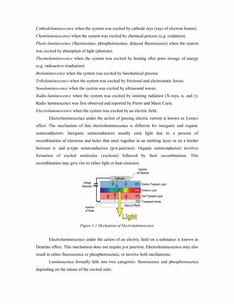
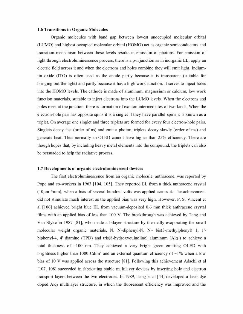
Electroluminescence when the system was excited by an electric field.
Electroluminescence under the action of passing electric current is known as Lossev
effect. The mechanism of this electroluminescence is different for inorganic and organic
semiconductors. Inorganic semiconductors usually emit light due to a process of
recombination of electrons and holes that meet together in an emitting layer or on a border
between n- and p-type semiconductors (p-n-junction). Organic semiconductors involves
formation of excited molecules (excitons) followed by their recombination. This
recombination may give rise to either light or heat emission.
Figure 1.1 Mechanism of Electroluminescence
Electroluminescence under the action of an electric field on a substance is known as
Destriau effect. This mechanism does not require p-n junction. Electroluminescence may also
result in either fluorescence or phosphorescence, or involve both mechanisms.
Luminescence formally falls into two categories: fluorescence and phosphorescence
depending on the nature of the excited state.

Fluorescence
In excited singlet states, the electron in the excited orbital is paired (by opposite spin)
to the second electron in the ground-state orbital. The return to the ground state is spin
allowed and occurs rapidly by emission of a photon. The emission rates of fluorescence are
typically 10-8 s, so that a typical fluorescence lifetime is near 10 ns (10 x 10-9 s). Because of
the short timescale of fluorescence, measurement of the time-resolved emission requires
sophisticated optics and electronics.
Phosphorescence
Phosphorescence is the emission of light from triplet excited states, in which the
electron in the excited state has the same spin orientation as the ground-state electron.
Transitions to the ground state are forbidden and the emission rates are slow (10 -3 to 100 s).
Following exposure to light, the phosphorescence substances glow for several minutes while
the excited phosphors slowly return to the ground state. Phosphorescence is usually not seen
in fluid solutions at room temperature. This is because there are many deactivation processes
that compete with emission, such as non-radiative decay and quenching processes. It should
be noted that the distinction between fluorescence and phosphorescence is not always clear.
Transition metal ligand complexes, which contain a metal and one or more organic
ligands, display mix singlet triplet states. These complexes display intermediate lifetimes of
hundreds of nanoseconds to several microseconds [14]. Fluorescence is a type of
photoluminescence that is generated when a photon of specific energy is absorbed by a
molecule wherein an electron within the molecule is promoted from the ground state to an
electronically excited state. The excited state can exist either as a singlet or triplet state. The
singlet excited state occurs when the electron is paired with another electron of opposing
spin. This is a quantum mechanically allowed transition, and fluorescence emission occurs as
a result of the spin-paired excited electron returning to the ground state. The triplet excited
state occurs when the excited electron is of the same spin as the second electron in the pair,
- ground
state. These processes which occur between the absorption and emission of light are usually
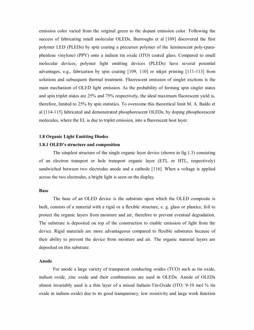
illustrated by Jablonski diagram shown in figure 1.2.
The singlet ground, first, and second electronic states are depicted as S0, S1, and S2,
respectively. At each of these electronic energy levels, the fluorophores can exist in a number
of vibrational energy levels, depicted as 0, 1, 2, etc. The transitions between states are
depicted as vertical lines to illustrate the instantaneous nature of light absorption. Transitions
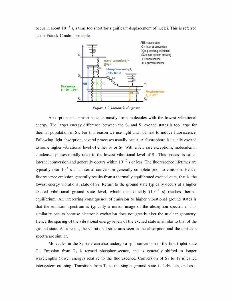
occur in about 10 15 s, a time too short for significant displacement of nuclei. This is referred
as the Franck-Condon principle.
Figure 1.2 Jablonski diagram
Absorption and emission occur mostly from molecules with the lowest vibrational
energy. The larger energy difference between the S0 and S1 excited states is too large for
thermal population of S1. For this reason we use light and not heat to induce fluorescence.
Following light absorption, several processes usually occur. A fluorophore is usually excited
to some higher vibrational level of either S1 or S2. With a few rare exceptions, molecules in
condensed phases rapidly relax to the lowest vibrational level of S1. This process is called
internal conversion and generally occurs within 10 12 s or less. The fluorescence lifetimes are
typically near 10 8 s and internal conversion generally complete prior to emission. Hence,
fluorescence emission generally results from a thermally equilibrated excited state, that is, the
lowest energy vibrational state of S1. Return to the ground state typically occurs at a higher
excited vibrational ground state level, which then quickly (10 12 s) reaches thermal
equilibrium. An interesting consequence of emission to higher vibrational ground states is
that the emission spectrum is typically a mirror image of the absorption spectrum. This
similarity occurs because electronic excitation does not greatly alter the nuclear geometry.
Hence the spacing of the vibrational energy levels of the excited state is similar to that of the
ground state. As a result, the vibrational structures seen in the absorption and the emission
spectra are similar.
Molecules in the S1 state can also undergo a spin conversion to the first triplet state
T1. Emission from T1 is termed phosphorescence, and is generally shifted to longer
wavelengths (lower energy) relative to the fluorescence. Conversion of S1 to T1 is called
intersystem crossing. Transition from T1 to the singlet ground state is forbidden, and as a

result the rate constants for triplet emission are several orders of magnitude smaller than
those for fluorescence. Molecules containing heavy atoms such as bromine and iodine are
frequently phosphorescent. The heavy atoms facilitate intersystem crossing and thus enhance
phosphorescence quantum yields [14].
Emission from the triplet state results in phosphorescence. This is rarely seen for
organic molecules in solution because these molecules are readily quenched by solution
species before emission. However, emission from triplet states is found with metal chelates
which have much shorter emission lifetimes than organic molecules.
The growing demand for photo luminescent and electroluminescent materials has
stimulated much fundamental material research in both organic and inorganic syntheses.
Transition metal complexes are finding broad potential applications in organic light-emitting
diodes [15], light-emitting diodes, light-emitting electrochemical cell [16], solar cells [17]
and sensors [18].
Due to their desirable optical, electronic and mechanical properties, these compounds
play an important role in developing semiconductors and optoelectronic devices.
There are several factors responsible for development of light emitting devices
(LEDs). The most important ones are brightness, available efficiency, flexibility, rugged
construction and low applied voltages. These are contributing to growth in markets such as
traffic lights, automotive brake signals, instrument and video displays and the many uses of
the new white LED-based products. A new development [19, 20] is directed to various
materials used for high brightness based on AlGaAs (red), AlInGaP (yellow-green to red) and
InGaN (blue, green and white) devices. Due to their epitaxial complexity the development of
LEDs depends on epitaxial growth advances in compound semiconductor technologies,
mainly molecular beam epitaxy (MBE) and metal-organic vapor phase epitaxy (MO VPE).
So, that the main engineering challenge is now the extraction or the ability to get all the light
out of the chip to where it is needed. Organic light-emitting diodes (OLEDs) look to supplant
the present standard of liquid crystal displays (LCDs) and solid-state light-emitting diodes
(LEDs) [21].
Following are the main limitations for inorganic type of LEDs
- limitation of area
- lattice matching problems
-difficult to extract light out of the devices

1.4 Inorganic phosphors
The inorganic phosphors generally consist of two parts, one is the host lattice and
another part is impurity which is also known as luminescent centre or dopant. Dopants are
present in very low concentration levels varying from few ppm up to one or two percent of
the host lattice. The phosphor is represented in a formula as given below:
Ab:D, C(0.02)
Where Ab represents host lattice and D represents an active center or dopant, in bracket its
concentration in moles is mentioned and C is the co-activator. For example - ZnS:Cu,
Cl(0.02), here ZnS is host lattice, Cu is activator whose concentration is 0.02 moles, Cl is a
co-activator.
There are different types of phosphors, which may be classified depending upon the
host lattice [22-29]. A few examples are aluminates - Sr4Al14O25: Eu2+,
Silicates - (Sr,Ba)Al2Si2O8:Eu2+, Phosphates - (Sr,Mg)2P2O7:Eu2+, Yttrate - Y2O3:Eu3+,
Titanate - BaTiO3: Pr3+ etc.
Inorganic electroluminescence involves use of inorganic direct band gap
semiconductors such as GaAs and ZnS.
1.5 Organic compounds as luminescent material
Organic materials as electroluminescent materials have attracted much attention in the
recent years because of their potential application in flat panel displays [30-33]. These
materials are classified according to their molecular structure in three types as:
I) Small molecules organic dyes (Dopant Emitters)
The small organic molecules organic dyes and dopant emitters like triphenyl diamines
(TPDs), oligothiophenes, rubrene, oxadiazoles, triazoles, porphyrines, perylenes, coumarines,
nile red etc., possess high fluorescent or phosphorescent quantum efficiency [34, 35]. They
are excited by energy transfer from the host emitter to give rise to various color emissions
like blue, green, yellow and white.
a) Green dye
Coumarin 6 was first used as host emitter with high fluorescence. One of the best
green dopants is 10-(2-benzothiazolyl)-1,1,7,7-tetramethyl-2,3,6,7-tetrahydro-1H,5H,11H-
[l]benzo-pyrano[6,7,8-ij]quinolizin-11-one, known as C-545T [36-38]. Another example of
green dopant used is N, N'- diethyl quinacridone (DEQ) [39].

O
S
N
N O
CH3
CH3
H3C CH3
C-545T
O O
N
S
N
Et
Et
N
N
O
O
C2H5
C2H5
Coumarin 6 DEQ
b) Yellow dye
Rubrene dye is commonly used as yellow dopant [40, 41].
Rubrene
c) Blue dye
Doped blue emitters used are 9,10-di (2-naphthyl) -DNA) and tetrakis (t-
butyl)perylene (TBPe) [42]. Another good blue emitter dopant is based on the basic structure
of distyrylarulene (DSA) host doped with a hole transporting amino substituted DSA dopant
[43].

TBPe -DNA
d) Red dye
Red dye DCM (4-dicyanomethylene-2-methyl-6-(p-dimethylaminostyryl) H-pyran
was reported first as a dopant in the tris(8-hydroxyquinolinato)aluminum (Alq3) layer. Nile
Red, perylene dicarboxymide derivatives, europium complexes, phorphyrin and other
materials have been used as red emitter dopants. [44-46].
N
ON O
Et
EtO
CNNC
H3C
NCH3
CH3
Nile Red DCM
II) Polymers
Polymers mainly used as electroluminescent materials are Guest-host polymers, Side-
chain polymers and -conjugated polymers.
- conjugated polymers are the most studied materials both from the chemical and the
physical point of view [47-50].
Different types of conjugated polymers are:
Orange-red emitting polymers:
*
n
OCH3
OCH2CH(C2H5)C4H9
Poly (2-methoxy-5-(2'-ethylhexoxy)-p-phenylene vinylene)
(MEH-PPV)

Yellow emitting polymers:
Poly[(9,9-dioctylfluorenyl-2,7-diyl)-alt-co-(1,4-benzo- -thiadiazole)]
(F8BT)
Green emitting polymers:
Poly (paraphenylenevinylene) (PPV)
Blue emitting polymers:
*
C8H17C8H17
n
Polyfluorene (PF)
III) Metal Chelates
Luminescent metal chelates have attracted tremendous attention due to their potential
applications in organic electronics -
transitions are dominant and responsible for color emission [51]. The choice of the metal ions
for luminescent metal chelates is limited to metals which do not exhibit d-d transition that
may interfere with the luminescence of the ligand. Therefore Lithium (I), Aluminum (III),
Boron (III), Beryllium (II), Zinc (II) has been ideal metal ions for their application in color
emission. These do not contain d-electrons, for zinc d-shell is completely filled and no d-d
transition is possible. The transitions in these metal chelates are ligand centered and metal
ions are used to stabilize the structure of the luminescent ligand. Metal complexes are placed
in the categories of organic materials known as organic semiconductors. Due to their
extremely low intrinsic conductivity most organic semiconductors should be designated as
insulators. The use of the name semi conductors is based on the extrinsic semiconducting
properties of organic systems such as transport of charge generated by light.

Several compounds have been used as luminescent materials, tris(8-hydroxyquinoline)
aluminum (Alq3) being one of the most important ones. Alq3 is an easily processed low-
molecular weight material, forming good quality amorphous films, which has been widely
used as the light emitting material in electronic devices. Moreover, Alq3 emits a bright green
luminescence and used as a green emitting medium in electroluminescent devices. Alq3 and
its analogues complexing Al with various substituted quinolines [52, 53] and complexes with
other bi and trivalent central ions (Be, B, Mg, Ca, Sr, Sc, Y, Cu, Zn, Eu, -diketones
complexes are used as light emitting metal chelate complexes.
Metal chelates of B(III), Al(III), Ga(III), In(III), Mg(II), Be(II), Zn(II), Ru(II), Eu(III),
Tb(III), Er(III), Dy(III) etc. have been used as EL materials for fabrication of OLEDs [54-
65]. OLEDs with trivalent europium [66], terbium [67] and thulium [68] complexes emit
monochromatic red, green and blue light, respectively. Trivalent samarium complex emit
orange color light [69] while neodymium and erbium complexes are used to obtain yellow
and orange lights [70] respectively. Within group III metals Al (III) is the most important
metal which emits green light in Alq3, the first metal complex used to develop multilayer
OLED. Boron also belongs to Group III like aluminum and having both metallic and non-
metallic characters. It forms complexes with coordination number three or four to give
efficient blue emission [71]. Be and Zn metals of Group II emits green light. Divalent Eu2+
has been used to demonstrate orange emission [72].
Lanthanide (III) ions especially in the middle of series i.e. Sm(III), Eu(III), Tb(III) and
transitions of central metal ion when excited by near UV radiations.
The metal ions that form complexes mainly with organic ligands 8-hydroxyquinoline
derivatives, diketones, porphyrines, poly aromatics, cryptands [73, 74], podands [75, 76],
carboxylic acid derivatives [77] and calixarenes [78-80] are luminescent materials.
Azomethine, 2-(2- -diketones
complexes belong to class of organic materials for use as organic electroluminescent
materials. Some important classes of such materials are discussed below:
Types of metal chelates
8-Hydroxyquinoline
The most common material that is used as light emitting material is the 3:1 complex
of 8- hydroxyquinoline with aluminum (Alq3) which is first of all reported by Tang and Van
Slyke [81]. Alq3 is thermally and morphologically stable to be evaporated into thin films,
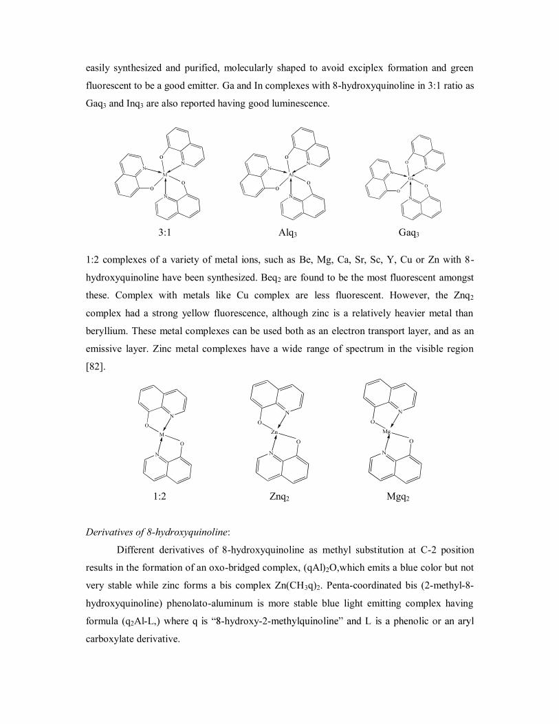
easily synthesized and purified, molecularly shaped to avoid exciplex formation and green
fluorescent to be a good emitter. Ga and In complexes with 8-hydroxyquinoline in 3:1 ratio as
Gaq3 and Inq3 are also reported having good luminescence.
N
O
Ga
NO
N
O
3:1 Alq3 Gaq3
1:2 complexes of a variety of metal ions, such as Be, Mg, Ca, Sr, Sc, Y, Cu or Zn with 8-
hydroxyquinoline have been synthesized. Beq2 are found to be the most fluorescent amongst
these. Complex with metals like Cu complex are less fluorescent. However, the Znq2
complex had a strong yellow fluorescence, although zinc is a relatively heavier metal than
beryllium. These metal complexes can be used both as an electron transport layer, and as an
emissive layer. Zinc metal complexes have a wide range of spectrum in the visible region
[82].
N
M
N
O
O
1:2 Znq2 Mgq2
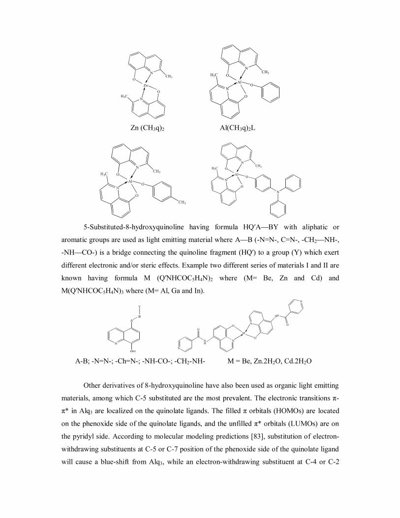
Derivatives of 8-hydroxyquinoline:
Different derivatives of 8-hydroxyquinoline as methyl substitution at C-2 position
results in the formation of an oxo-bridged complex, (qAl)2O,which emits a blue color but not
very stable while zinc forms a bis complex Zn(CH3q)2. Penta-coordinated bis (2-methyl-8-
hydroxyquinoline) phenolato-aluminum is more stable blue light emitting complex having
formula (q2Al- -hydroxy-2-
carboxylate derivative.
N
Zn
N
O
OCH3
H3C
NAl
N
OCH3
O
H3C
O
Zn (CH3q)2 Al(CH3q)2L
33
3
NAl
N
OCH3
O
H3C
O
N
5-Substituted-8- BY with aliphatic or
aromatic groups are used as light emitting material where A B (-N=N-, C=N-, -CH2 NH-,
-NH CO-) is a bridge connecting
different electronic and/or steric effects. Example two different series of materials I and II are
known having formula M 5H4N)2 where (M= Be, Zn and Cd) and
5H4N)3 where (M= Al, Ga and In).
N
NH
O
N
O
N
ON
O
M
A-B; -N=N-; -Ch=N-; -NH-CO-; -CH2-NH- M = Be, Zn.2H2O, Cd.2H2O
Other derivatives of 8-hydroxyquinoline have also been used as organic light emitting
materials, among which C- -
3 located
the pyridyl side. According to molecular modeling predictions [83], substitution of electron-
withdrawing substituents at C-5 or C-7 position of the phenoxide side of the quinolate ligand
will cause a blue-shift from Alq3, while an electron-withdrawing substituent at C-4 or C-2

position of the pyridyl side will cause a red-shift. The direction of the spectral will be
reversed if the substituents are electron-donating instead at the respective positions.
N
NH
ON
O
N
NH
O
N
O
N
HNO
NO
M
M = Al, Ga, In
4-Hydroxy-1, 5-naphthyridine and 5-hydroxyquinoline have also been used as organic light
emitting materials, among which the C-5 substituted are the most prevalent. Bidentate ligand
o-(N-phenyl-2-benzimidazolyl) phenol, complexes with Al3+ and Be2+ to form stable,
thermally evaporable, and blue-emitting metal complexes, abbreviated as Al(PBI)3 and
Be(PBI)2, respectively.
Benzoquinolinolato complexes
Beryllium complex with 10-hydroxybenzo[h] quinoline (Bebq2) has been found to have a
very strong green fluorescence and thermally stable which are useful as electroluminescent
material.
N
ON
OBe
Bebq2
Azomethine-metal complexes
Metal complexes with azomethine ligands are used as blue electroluminescent
materials. For example, 2:1 and 1:1 metal complexes of zinc are bis (N-methylsalicylidene
amino) zinc (II) [2AZM-Me] and N, -disalicylidene hexane-1, 6-diaminato zinc (II)

[1AZM-hex] respectively [84]. Bis (2-(2- hydroxyphenyl) benzothiazolato) zinc, Zn (BTZ)2
complex is also a bright greenish white color emitting material [85].
CH
O
N
CH3
O
N
H3C
CH
Zn
O
N(H2C)6
CHHNHC
OZn
2AZM-Me 1AZM-hex
Metal chelate complexes like bis (2-(2-hydroxyphenyl) benzoxazolate) zinc
[Zn(BOX)2], bis(2-(2-hydroxyphenyl)benzothiazolate)zinc [Zn(BTZ)2] and tri(4-
phenanthridinolate) aluminum (Alph3) are also used as light emitting materials. These
complexes chelate through phenolic oxygen which is doubly bound to nitrogen to Zn or Al.
N
S
O
N
S
O Zn
Zn(BTZ)2
Metal complexes of polycyclic aromatic or fused ring ligand
The oxadiazole, thiadiazole, phenylpyrizine, benzimidazole groups and phenyl-
substituted quinoline polycyclic ligands are also used as the fused ring ligand for metal
complex formation. These complexes are used as light emitting materials for display
applications. 2-(2-Hydroxyphenyl)-5-phenyloxadiazole (ODZ) and 1-phenyl-2-(2-
hydroxyphenyl) benzimidazole (BIZ) chelates such as Zn (ODZ)2, Zn(BIZ)2 and Al(ODZ)3
have been found to be useful as electron-transport emitters in the blue region [86]. Bis [2-(2-
hydroxyphenyl) pyridine] beryllium (Bepp2) and bis (10-hydroxybenzo[h]qinolinato)
beryllium (Bebq2) are reported as strong green fluorescence emitter [87]. The diphenyl boron
analogs of Alq3 (Ph2Bq) have also been used as light emitting materials. (8-
Hydroxyquinolinolato) lithium (Liq) and (2-methyl-8-hydroxyquinolinolato) lithium (LiMeq)
have also been found to be useful emitter materials [88]. Metal complexes of POP = 2-(5-
phenyl-1,3,4-oxadiazol-yl)phenonate; PBO = 2-(2-hydroxyphenyl)benzoxazolato; 2-(2-
hydroxyphenyl)-5-phenyl-1, 3-oxazole; (PPO) and NOP = 2-(5-naphthyl-1,3,4-
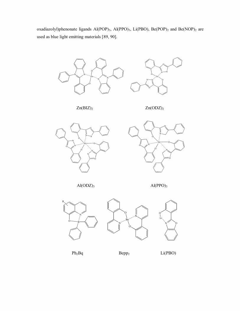
oxadiazolyl)phenonate ligands Al(POP)3, Al(PPO)3, Li(PBO), Be(POP)2 and Be(NOP)2 are
used as blue light emitting materials [89, 90].
N N
O
NN
O
Zn
O
NN O
O
N NO
Zn
Zn(BIZ)2 Zn(ODZ)2
O N
N
O
O
N NO
O
NN
OAlO N
O
O
NO
O
N
OAl
Al(ODZ)3 Al(PPO)3
N
O B
R
N
ON
O
BeN O
O
Li
Ph2Bq Bepp2 Li(PBO)
O
NN O
O
N NO
Be
Zn(Phq)2 Be(POP)2
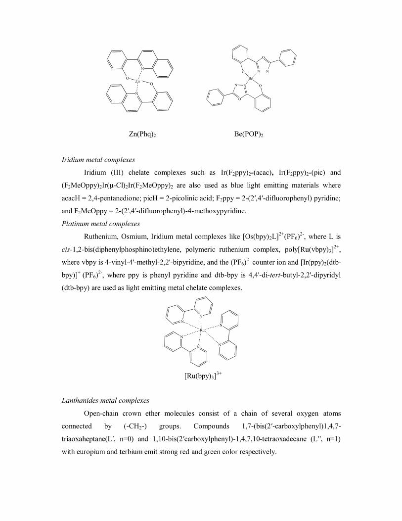
Iridium metal complexes
Iridium (III) chelate complexes such as Ir(F2ppy)2-(acac), Ir(F2ppy)2-(pic) and
(F2MeOppy)2 -Cl)2Ir(F2MeOppy)2 are also used as blue light emitting materials where
acacH = 2,4-pentanedione; picH = 2-picolinic acid; F2ppy = 2- -difluorophenyl) pyridine;
and F2MeOppy = 2- -difluorophenyl)-4-methoxypyridine.
Platinum metal complexes
Ruthenium, Osmium, Iridium metal complexes like [Os(bpy)2L]2+(PF6)2-, where L is
cis-1,2-bis(diphenylphosphino)ethylene, polymeric ruthenium complex, poly[Ru(vbpy)3]2+,
where vbpy is 4-vinyl-4'-methyl-2,2'-bipyridine, and the (PF6)2- counter ion and [Ir(ppy)2(dtb-
bpy)]+ (PF6)2-, where ppy is phenyl pyridine and dtb-bpy is 4,4'-di-tert-butyl-2,2'-dipyridyl
(dtb-bpy) are used as light emitting metal chelate complexes.
NN
N
NN
N
Ru
[Ru(bpy)3]3+
Lanthanides metal complexes
Open-chain crown ether molecules consist of a chain of several oxygen atoms
connected by (-CH2-) groups. Compounds 1,7-(bis -carboxylphenyl)1,4,7-
1,10-b -1,4,7,10-
with europium and terbium emit strong red and green color respectively.

1, 7- -carboxylphenyl)-1, 4, 7-
1, 10-Bis -carboxylphenyl)-1, 4, 7, 10-
Europium complexes of 3-aminopyridine-2-carboxylic acid and mono
hexadecylphthalic acid are used as red light emitting whereas terbium complexes of mono
hexadecyl p-aminobenzoic acid and pyridine -2, 6-dicarboxylate dianion are used as green
color light emitting materials.
Lanthanide metals form light emitting complexes with -diketone. These types of
complexes are denoted by formula [Ln(L)3B complexes] where Ln is lanthanides, -
diketone and B is a Lewis base such as 1,10- -bipyridine (bipy). A
few important lanthanide complexes are; Eu(Btfa)3.2H2O; Eu(Btfa)3o-phenNO; Eu(3-
NH2pic)32H2O Eu(3-NH2pic)3o-phen; Eu(DPM)3o-phen; Eu(TTA)32H2O; Eu(TTA)3DBSO
where TTA = thenoyltrifluoroacetonate; DBSO = dibenzylsulfoxide; 3- NH2pic = 3-
aminopyridine-2-carboxylic acid; DPM = dipivaloylmethane; bzac =1-phenyl-1,3-
butanedione; btfa =4,4,4-trifluoro-1-phenyl-1,3-butanedione); DBM = Dibenzoylmethane; o-
phen = 1,10-phenanthroline; DB- -Di-tertbutyl- -dipyridyl; DN-bpy = -
Dinonyl- - -Biquinoline; terpyridine (terpy). Complexes of Eu(III) and
Tb(III) with pyridine carboxylic acids and their N-oxides have shown to be powerful
sensitizers of the Ln(III) luminescence [91-102]. Systems bearing N-oxide groups further
more form more stable complexes with lanthanides than the parent ligands and have unique
luminescence properties, such as long luminescence.
N
N
MO
O
CH3
3
N
N
MO
O
CH3
3

M = Tb, Eu, Dy, Gd
Polynuclear d10 metal complexes
Di- and tri-phosphines as bridging ligands are also used as light emitting materials.
The triphosphine ligand bis(dimethylphosphinomethyl)methylphosphine, dmmp complexes
with three Au(I) centres and the dinuclear [Au2(dmpm)2]2+ [dmpm =
bis(dimethylphosphino)methane] and trinuclear [Au3(dmmp)3]3+ have been reported. These
polynuclear gold (I) phosphine complexes are strongly luminescent [103].
PH PH
Au
HP
Au
PH
2+
[Au2 (dmpm)2]2+ [Au2(dmmp)3]2+ [Au3(dmpm)3]3+
[Au3 (dmmp)3]3+
1.6 Transitions in Organic Molecules
Organic molecules with band gap between lowest unoccupied molecular orbital
(LUMO) and highest occupied molecular orbital (HOMO) act as organic semiconductors and
transition mechanism between these levels results in emission of photons. For emission of
light through electroluminescence process, there is a p-n junction as in inorganic EL, apply an
electric field across it and when the electrons and holes combine they will emit light. Indium-
tin oxide (ITO) is often used as the anode partly because it is transparent (suitable for
bringing out the light) and partly because it has a high work function. It serves to inject holes
into the HOMO levels. The cathode is made of aluminum, magnesium or calcium, low work
function materials, suitable to inject electrons into the LUMO levels. When the electrons and
holes meet at the junction, there is formation of exciton intermediates of two kinds. When the
electron-hole pair has opposite spins it is a singlet if they have parallel spins it is known as a
triplet. On average one singlet and three triplets are formed for every four electron-hole pairs.
Singlets decay fast (order of ns) and emit a photon, triplets decay slowly (order of ms) and
generate heat. Thus normally an OLED cannot have higher than 25% efficiency. There are
though hopes that, by including heavy metal elements into the compound, the triplets can also
be persuaded to help the radiative process.
1.7 Developments of organic electroluminescent devices
The first electroluminescence from an organic molecule, anthracene, was reported by
Pope and co-workers in 1963 [104, 105]. They reported EL from a thick anthracene crystal
-5mm), when a bias of several hundred volts was applied across it. The achievement
did not stimulate much interest as the applied bias was very high. However, P. S. Vincent et
al [106] achieved bright blue EL from vacuum-deposited 0.6 mm thick anthracene crystal
films with an applied bias of less than 100 V. The breakthrough was achieved by Tang and
Van Slyke in 1987 [81], who made a bilayer structure by thermally evaporating the small
molecular weight organic materials, N, N'-diphenyl-N, N'- bis(3-methylphenyl) 1, 1'-
biphenyl-4, 4' diamine (TPD) and tris(8-hydroxyquinoline) aluminum (Alq3) to achieve a
total thickness of ~100 nm. They achieved a very bright green emitting OLED with
brightness higher than 1000 Cd/m2 and an external quantum efficiency of ~1% when a low
bias of 10 V was applied across the structure [81]. Following this achievement Adachi et al
[107, 108] succeeded in fabricating stable multilayer devices by inserting hole and electron
transport layers between the two electrodes. In 1989, Tang et al [44] developed a laser-dye
doped Alq3 multilayer structure, in which the fluorescent efficiency was improved and the
emission color varied from the original green to the dopant emission color. Following the
success of fabricating small molecular OLEDs, Burroughs et al [109] discovered the first
polymer LED (PLEDs) by spin coating a precursor polymer of the luminescent poly-(para-
phenlene vinylene) (PPV) onto a indium tin oxide (ITO) coated glass. Compared to small
molecular devices, polymer light emitting devices (PLEDs) have several potential
advantages, e.g., fabrication by spin coating [109, 110] or inkjet printing [111-113] from
solutions and subsequent thermal treatment. Fluorescent emission of singlet excitons is the
main mechanism of OLED light emission. As the probability of forming spin singlet states
and spin triplet states are 25% and 75% respectively, the ideal maximum fluorescent yield is,
therefore, limited to 25% by spin statistics. To overcome this theoretical limit M. A. Baldo et
al [114-115] fabricated and demonstrated phosphorescent OLEDs, by doping phosphorescent
molecules, where the EL is due to triplet emission, into a fluorescent host layer.
1.8 Organic Light Emitting Diodes
1.8.1
The simplest structure of the single organic layer device (shown in fig.1.3) consisting
of an electron transport or hole transport organic layer (ETL or HTL, respectively)
sandwiched between two electrodes anode and a cathode [116]. When a voltage is applied
across the two electrodes, a bright light is seen on the display.
Base
The base of an OLED device is the substrate upon which the OLED composite is
built, consists of a material with a rigid or a flexible structure, e. g. glass or plastics; foil to
protect the organic layers from moisture and air, therefore to prevent eventual degradation.
The substrate is deposited on top of the construction to enable emission of light from the
device. Rigid materials are more advantageous compared to flexible substrates because of
their ability to prevent the device from moisture and air. The organic material layers are
deposited on this substrate.
Anode
For anode a large variety of transparent conducting oxides (TCO) such as tin oxide,
indium oxide, zinc oxide and their combinations are used in OLEDs. Anode of OLEDs
almost invariably used is a thin layer of a mixed Indium-Tin-Oxide (ITO: 9-10 mol % tin
oxide in indium oxide) due to its good transparency, low resistivity and large work function
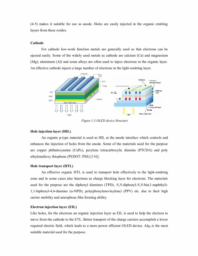
(4-5) makes it suitable for use as anode. Holes are easily injected in the organic emitting
layers from these oxides.
Cathode
For cathode low-work function metals are generally used so that electrons can be
ejected easily. Some of the widely used metals as cathode are calcium (Ca) and magnesium
(Mg); aluminum (Al) and some alloys are often used to inject electrons in the organic layer.
An effective cathode injects a large number of electrons in the light-emitting layer.
Figure 1.3 OLED device Structure
Hole injection layer (HIL)
An organic p-type material is used as HIL at the anode interface which controls and
enhances the injection of holes from the anode. Some of the materials used for the purpose
are copper phthalocyanine (CuPc), perylene tetracarboxylic diamine (PTCDA) and poly
ethylenedioxy thiophene (PEDOT: PSS) [116].
Hole transport layer (HTL)
An effective organic HTL is used to transport hole effectively to the light-emitting
zone and in some cases also functions as charge blocking layer for electrons. The materials
used for the purpose are the diphenyl diamines (TPD), N,N-diphenyl-N,N-bis(1-naphthyl)-
1,1-biphenyl-4,4-diamine -NPD), poly(phenylenevinylene) (PPV) etc. due to their high
carrier mobility and amorphous film forming ability.
Electron injection layer (EIL)
Like holes, for the electrons an organic injection layer as EIL is used to help the electron to
move from the cathode to the ETL. Better transport of the charge carriers accomplish a lower
required electric field, which leads to a more power efficient OLED device. Alq3 is the most
suitable material used for the purpose.

Electron transport layer (ETL)
The ETL is an n-type doped organic material that transports the electron. Both
quinoxalines and quinolines are electroluminescent materials, allowing these compounds to
be used as the electron-transport and emitting layers in devices [118, 119]. Zinc quinolates
are also used as electron transport materials with better efficiency. Alq3 is the most suitable
material as ETL.
Emitting layer (EML)
The emitting layer provides the levels for hole, injected from anode and electron,
injected from cathode to recombine and decay radiativley. Materials used for this are PPVs,
polyfluorene, ladder polymers, dendrimer and small molecules like metal chelates and
oligomers.
1.8.2 Electroluminescent materials used for OLEDs
Generally the materials used for the fabrication of organic light emitting diodes are of
organic origin and semi conducting in nature. During the fabrication of the OLED it is
important to select an appropriate organic electroluminescent material for proper function and
best performance and high efficiency. The organic electroluminescent materials are broadly
divided into two parts.
a) Small Molecular Materials (Low molecular weight compounds).
b) Macromolecular Materials (High molecular weight polymers).
a) Small molecular Materials
Small molecules are the molecular structures of relatively low molecular weight.
These can be used as such or blended into a polymer matrix or grafted into a polymer
backbone so that they can be applied easily by spin coating. The requirements for an organic
small molecule or complex to be used in the form of an emission layer in the device are that it
should be thermally stable to enable vacuum deposition, highly luminescent in the solid-state,
amorphous in nature and should be thin-film forming. It should also be able to transport
electrons with the desired efficiency. In small molecules many classes of complexes like
complexes of 8-hydroxyquinoline and its derivatives with different metals like aluminum,
gallium, indium, zinc and rare earth complexes with -diketones are well known [120]. Alq3
was the first metal complex which was used as light emitting material in OLEDs [81].
b) Macromolecular Materials
Macromolecular materials are conjugated polymers of high molecular weight
composed of a long repeating chain of similar smaller molecules called monomers. They
possess molecular weight twenty to fifty times higher than small molecules. Besides their
roles as inert binders, polymers have been used in OLEDs as electroluminescent materials
since the late 1980s, when emission was observed in poly (1, 4-phenylenevinylene) [121].
Polymers in OLEDs are used as emissive as well as hole transport layers and electron
transport layers. Smallest basic unit i.e monomer acts as the light emitting center in polymers.
Polymers light emitting materials are easily deposited by spin coating method.
1.8.3 Advantages of organic materials in electroluminescence processes
The application of organic compounds as active components in electronic devices is
very important. Since the discovery of electroluminescence in thin film organic layers device
by Van Slyke and Tang from Kodak in 1987, there has been special interest in the new
organic phosphors [81]. Organic materials
have some advantages over other luminescent materials, such as:
1. The organic materials are usually used as thin amorphous films, which can be
processed easily over large areas.
2. Size of organic materials are relatively small (100 nm) and large-scale production
(chemistry) is easier than for inorganic materials (growth processes of single crystals
etc.).
3. They can be tuned chemically in order to adjust the band gap, charge transport as well
as solubility and several other structural properties.
4. The vast variety of possible chemical structures and functionalities of organic
materials (polymers, oligomers, dendrimers, dyes, pigments, liquid crystals, etc.)
favor an active research for alternative competitive materials with the desired
properties.
5. The unique about organic material over the inorganic ones is that their emission bands
are significantly red-shifted from their absorption bands, which is known as the
Stokes shift [122].

6. Large amount of organic materials are known to have extremely high fluorescence
quantum efficiencies in the visible spectrum, including the blue region, some
approaching 100% efficiency.
7. Being organic in nature they have an eco-friendly impact on environment i.e.
biodegradable.
1.8.4 Basic principle of OLEDs
The basic principle of an OLED includes the injection of electrons from the cathode
and injection of holes from the anode. When a voltage is applied to the electrodes the charges
start moving in the device under the influence of the electric field. Electrons and holes move
in opposite direction. The recombination followed by the radiative decay of the excited
electron-hole state or exciton leads to the creation of a photon with a frequency given by the
energy gap ( ) between the LUMO and HOMO levels of the emitting molecules.
Therefore, the electrical power applied to the electrodes is transformed into light. The color
of the light emitted during this process is determined by the band gap of the exciton.
1.8.5 Working of OLEDs
OLEDs work on the principle of electroluminescence. Electroluminescence (EL) is an
optical phenomenon and electrical phenomenon in which material emits light in response to
an electric current passed through it, or to a strong electric field. In its simplest form
electroluminescence is the conversion of electrons into photons.
Firstly, the anode is kept positive with respect to the cathode. There occurs an electron
flow from the cathode to the anode. This electron flow is captured by the emissive layer
causing the anode to withdraw electrons from the conductive layer. Thus, there occurs a flow
of holes in the conductive layer. As the process continues, the conductive layer becomes
positively charged and the emissive layer becomes negatively charged.
A combination of holes and electrons occur due to electrostatic forces. As the
electrons are less mobile than the holes, the combination normally occurs very close to the
emissive layer. This process produces light in the emissive region after there has been a drop
in the energy levels of the electrons. The light produced by the emissive layer has a frequency
in the visible region. The color of the light produced can be varied according to the type of
organic molecule used for its process. To obtain color displays, a number of organic layers
are used. Another factor of the light produced is its intensity. If more current is applied to the
OLED, the brighter the light appears, i.e. with the increase in voltage luminescence increases.

The process of electroluminescence in an OLED device takes place into four steps:
Figure 1.4 Electroluminescence process in OLED device
1) Introduction of carriers into device
The electrodes upon application of an electric field from battery or power supply of
OLED inject charge carriers into the material.
2) Movement of the carriers
Once electrons are injected, they drift to the electrode of more posit ive potential. At
the same time, holes are injected by the anode into the highest occupied molecular orbital
(HOMO) of the active material analogous to the valence band (Ev) in the semiconductors.
Injection of holes corresponds to the removal of electrons from electro active material i.e.
oxidation of the electro active material.
3) Excitation of the radiative material
Holes and electrons recombine in the active material producing an excited state called
exciton on the emitting material which decays radiatively to emit light. An exciton is a bound
state of an electron and a hole, leading to a zero net charge.
4) Radiative relaxation of the excited material
electron, a photon is emitted. When this happens, the electron gives up energy in the form of
light from the emissive layer in the OLED.
This process can be understood by the mechanism given in fig. 1.4.
1.8.6 Device Efficiency
The efficiency [122] of OLEDs can be characterized by its
a. Quantum efficiency,
b. Power efficiency (lm/W),
c. Luminous efficiency (Cd/A), sometimes called luminous yield.
a. Quantum efficiency
q has two parts: internal and external:
(i) Internal quantum int or IQE is the number of photons generated
inside the device per number of injected hole electron pairs. A large fraction of
generated photons stays trapped and absorbed inside the device.
(ii) ext or EQE is the number of photons released
from the device per number of injected hole electron pairs.
b. Power efficiency (lm/W)
p is the ratio of the lumen output to the input electrical
watts (lm/W).
c. Luminous efficiency (Current efficiency) (Cd/A)
represents the ratio of the lumen output to the optical watts (radiative
power). The luminous efficiency and luminous efficacy of a device account for a spectral
sensitivity of a human eye. Therefore, two devices with similar quantum efficiencies can

have different luminous performance, depending on the spectrum of the emitted light. In the
process of converting electrical power into optical power, losses are incurred due to non-
radiative processes (thermal relaxation of excitons, internal reflection and absorption of
photons).
1.8.7 Light Emission in OLEDs
In an electroluminescent device, the electrons migrate toward the anode, but at some
point meet a hole, thus creating an exciton. The exciton consists of four states, one singlet
and three triplet states that appear as four quasi-degenerate states at large hole electron
separation distances. Statistically, all four states will be populated with equal probability.
When the hole and the electron are on the same molecule, the states are no longer degenerate,
and 1:3 ratio of singlet to triplets is seen. In organic molecules where the spin orbit coupling
(SOC) is small, emission is usually observed by recombination of the electrons in the singlet
excited state with the holes, and the exciton in the triplet state return to the ground state
through non-radiative decay pathways. Thus, only 25% of the injected electrons result in
emitted light in fluorescent molecules. However, if the SOC is large, the exciton of the singlet
state will experience intersystem crossing to the triplet state, and emission from all excitons
in the triplet state may occur. Hence, 100% efficiency may be obtained, compared with only
25% when the SOC is small [124, 125]. Molecules containing heavy metals display
phosphorescent emission from the triplet state because of the presence of strong SOC and for
this reason much research into emitters containing heavy metals has been done.
1.8.8 Types of OLED displays
I) Passive-matrix OLED (PMOLED)
The passive-matrix OLEDs have stack layers of cathode, organic and anode in a linear
pattern hode are superimposed
of anode to form a two dimensional array of pixels. Pixel is the intersecting point
of cathode and anode where light is emitted from organic material which is sandwiched
between cathode and anode. Organic materials and
structure (base and pillar). The design of this type of OLED makes them more suitable for
small screen devices like cell phones, MP3 players and so on. Though this type is less power

II) Active-matrix OLED Displays (AMOLED)
Active-matrix OLED has an integrated electronic back plane as its substrate and lends
itself to high-resolution, high-information content applications like videos and graphics. This
type of display is made possible by the use of poly silicon technology, which because of its
high carrier mobility; provide thin film transistors (TFT) with high current carrying capability
and high switching speed. In active-matrix OLED display, each individual pixel can be
addressed independently via the the electronic back plane.
Each pixel duration of
the video. This type of OLED is suitable for high resolution and large size display.
III) Transparent OLEDs (TOLEDs)
Transparent OLEDs have only transparent components i.e. substrate, cathode and anode.
TOLEDS can be up to 85% transparent when switched off, nearly as clear as the glass or
plastic on which they are built. Transparent OLEDs allows light to pass in both directions
when turned on. Therefore transparent OLEDs are of both types top emitting and bottom
emitting. Transparent OLED display can be either active-matrix or passive-matrix. These
devices have a good contrast even in bright sunlight so are applicable in head-up displays,
mobile phones, smart windows and so on.
IV) Top-emitting OLEDs
Top-emitting OLEDS are like transparent OLEDs with only difference having opaque
substrates in active-matrix displays. Top-emitting structure can improve the effective area
and the power consumption in the high-resolution active-matrix OLED displays by directing
the emitted light away from the thin film transistor (TFT) backplane rather than through it.
Such devices are suitable for matrix applications like smart cards.
V) Flexible or Foldable OLEDs
Flexible OLEDs are organic light emitting devices having flexible base substrates like
metallic foils or plastics. FOLEDs have advantages over LCD displays which are built on
rigid glass substrates and contain a bulky back light. This type is mainly used in devices
which have more chance of breaking. Flexible metallic substrates provide excellent barrier
properties, thermal and dimensional stability over a broad temperature range and cost-
effectiveness so these can be sewn into fabrics for
and OLED displays.

Figure 1.5 Flexible OLED
VI) Stacked OLEDS (SOLEDs)
The SOLEDs are based on stacking the red, green, and blue sub pixels on top of one
another, instead of side-by-side as is the common configuration for CRTs and LCDs, in a
vertically integrated OLED structure where intensity, color and gray scale can be
independently tuned to achieve high resolution full-color. Stacked OLED is best approach to
achieve full color. SOLED is possible only for small molecules, due to the fact that
complicated multi-layer structure is not appropriate for OLED devices based on conjugated
polymers [126].
Figure 1.6 Stacked OLED
VII) Phosphorescent OLEDs
Phosphorescent organic light emitting device (PHOLED) is a display technology that uses
soluble phosphorescent small molecule materials to create organic light emitting devices
(OLEDs). PHOLED products are developed for general lighting application. PHOLED based
lighting sources, such as glowing walls are expected to provide cost-effective and energy
efficient alternatives to traditional incandescent and fluorescent lighting.
VIII) White OLEDs

These emit white light that is brighter, more uniform and more energy efficient than
fluorescent lights. White OLEDs have true-color qualities of incandescent lighting. White
OLEDs can replace fluorescent lights used currently in homes and buildings. As OLEDs can
be made in large sheets, their use will reduce energy costs for lighting. White light emitting
devices architectures offer a range of spectral coverage, color temperature and efficiency
profiles. These devices create the brightest light of all. These are manufactured in large sheets
and are also cost-effective.
Figure 1.7 White OLED
IX) Full color OLEDs
The best approach to achieve full-color is through the stacked OLED (SOLED) device
and is only possible for small molecules because a complicated multi-layered structure is not
appropriate for OLED devices based on conjugated polymers. Three separately addressed
devices are placed on top of each other. The bottom and the middle device are transparent
OLED (TOLEDs), allowing down emitting light from the top layer.
Figure 1.8 RGB OLED
1.8.9 Fabrication of OLEDs devices
Fabrication of organic light emitting devices needs a pure deposition of organic
material on a cleaned substrate. Moisture and UV-light may degrade mechanism of the device
during manufacturing; hence care has to be taken during manufacture [127].
Following techniques are used for fabricating the OLED devices:
(i) Vacuum deposition or vacuum thermal evaporation (VTE)
Small molecules are deposited through this process by coating a substance to form
thin films. The evaporation process results in parallel surface, important for lifetime of
device. Good uniformity and purity is achieved by sputtering process. Organic material is
sputtered as thin film on the substrate by bombardment of ions which ejects atoms and
molecules from organic solution into a vacuum chamber. The atoms and molecules will form
a thin film at the substrate. As the heating method is complicated and the strictness of
parameters should be highly accurate, this method is economical as well.
(ii) Organic vapor phase depositions (OVPD)
High quality organic films with better performance and at lower cost than
conventional vacuum thermal evaporation (VTE) process are deposited by OVPD. In OVPD
an inert gas carrier is used to transfer organic films on to a cooled substrate in a low-pressure,
hot-walled reactor chamber. The organic materials are stored in external, separate, thermally-
controlled cells. The materials evaporated from these heated cells are transported by an inert
carrier gas such as nitrogen, using gas flow rate, pressure and temperature as process control
variables. The materials deposit down onto the cooled substrate. This is also an efficient
technique which can be carried out at a low cost.
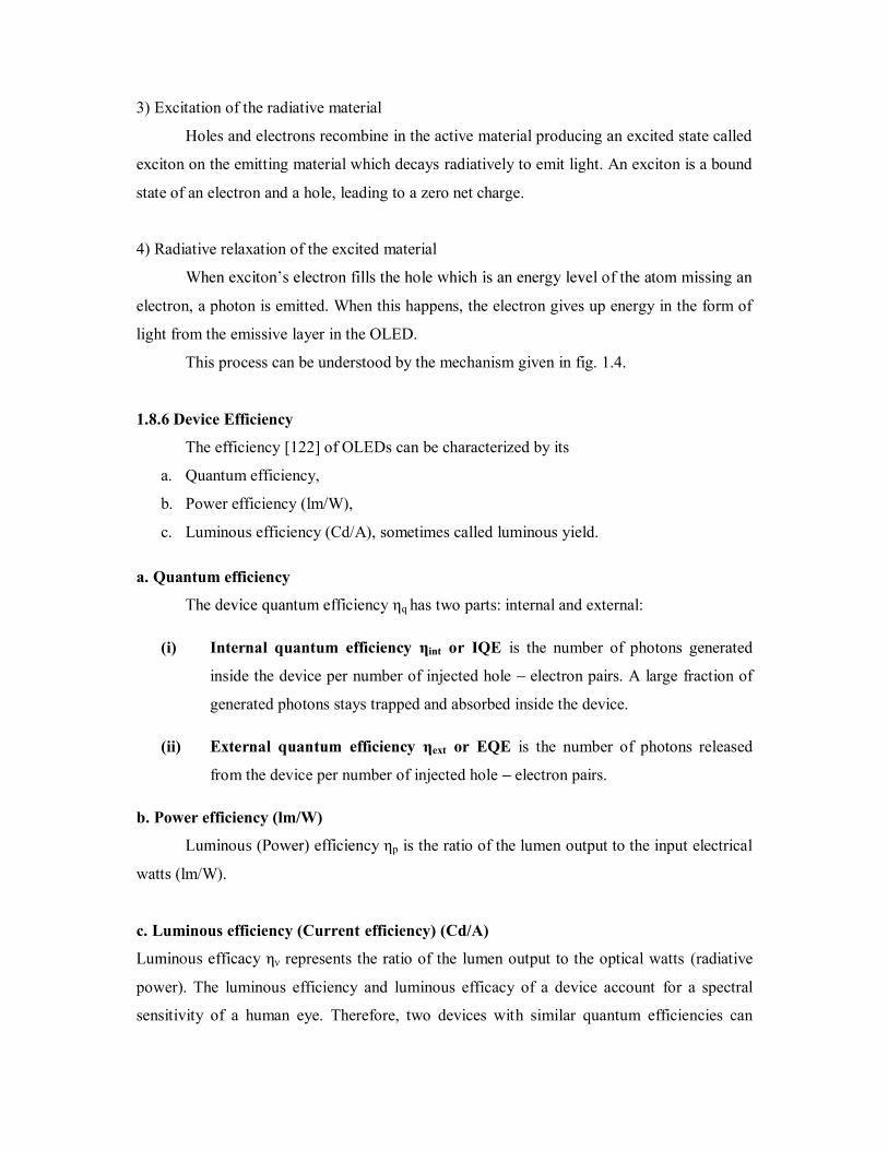
(iii) Inkjet printing
This is the cheapest and most commonly used technique. Organic layers are sprayed
onto substrates just like inks are sprayed onto paper during printing. Inkjet technology greatly
reduces the cost of OLED manufacturing and allows OLEDs to be printed onto very large
films for large displays like 80-inches screens or electronic billboards.
(iv) Dip-coating
In dip coating method the substrate is slowly dipped into the polymer resulting in a
cover of polymers at both sides. This is also a popular way of creating thin films where it is
generally used for applying films onto flat or cylindrical substrates.
(v) Spin-coating
In spin coating method a drop of polymer solution placed onto a rotating plate where
the polymer solution is spread out to form a uniform thin film at room temperature. Drops

formed may result in non smooth and non-parallel surfaces and causing degradation of device
because of different distances between the electrodes. Spin coating is widely used in micro
fabrication, where it can be used to create thin films with thicknesses below 10 nm. It is used
intensively in photolithography to deposit layers of photo resist about 1 micrometre thick.
1.8.10 Advantages of OLEDs
Organic light emitting devices are now coming out of laboratory trials and since last
few years they have been applied in the microelectronic gadgets to enhance efficiency and
lifespan of the gadget. The miniaturization of the electronic gadgets in future will be possible.
During the last decade, an explosive growth of activity in the area of organic
electroluminescence has occurred in both academia and industry, stimulated by the promise
of light-emitting plastics for the fabrication of large, flexible, inexpensive and efficient
screens to be used in different applications. The most advantageous thing going to happen is
that the shape and size of illumination system will change dramatically. Some of the most
important advantages that will lead the development of the OLEDs as one of the feasible
technologies are:
Flexible
It is possible to make OLED displays flexible by using the right materials and
processes.
Very thin
OLED displays can be made very thin, making them very attractive for televisions
and computer monitor applications.
Color capability
It is possible to fabricate OLED displays that can generate all colors.
Power consumption
The power consumed by an OLED display is generally less than that of an LCD
when including the backlight required. This is only true for backgrounds that are dark or
partially dark.
Bright images
OLED displays can provide a higher contrast ratio than that obtainable with an LCD.
Because of unsurpassed contrast and luminance of OLEDs, bright images and videos are easy
to see from any angle. OLED screens appear extra ordinarily bright due to their high contrast.
They have neither backlights nor chemical shutters that must open and close like in LCDs.
Instead each pixel illuminates like a light bulb.

Figure 1.9 Bright OLED
Wide viewing angle
With many displays, the color becomes disported and the image less saturated as the
viewing angle increases. Colors displayed by OLEDs appear correct, even up to viewing
angles approaching 90°. OLED displays brightness and clarity produce the consistent quality
image from almost any angle, therefore easy to see. OLED screens provide a clear and
distinct image even in bright light.
Fast response time
As LCDs depend upon charges being held in the individual pixels, they can have a
slow response time. OLEDs are very much faster. A typical OLED can have a response time
of less than 0.01ms. The response time for OLEDs is shorter than 1
for active matrix LCDs and 300 ms for passive addressed LCDs [128, 129]. The fast response
time for OLEDs make them possible for use in video application even in passive matrix
addressing, which is not possible for LCDs.
Low cost in the future
OLED fabrication is likely to be able to utilise techniques that will enable very low
cost displays to be made, although these techniques are still in development. Current costs of
course are high. Roll-to-roll manufacturing process, such as inkjet printing and screen
printing, are possible for polymer OLEDs. OLEDs are up to 20% to 50% cheaper than LCD
processes. Plastics will make the OLED tougher and more rugged. These OLED could be
cturing of OLED is cheap and
not wasteful [130]. LCD manufacturing is more expensive due to need of expensive
components like color filters, polarizers and backlight.
Robust Design
OLEDs are tough enough to use in portable devices such as cellular phones, digital video,
cameras, DVD players, car audio equipment and personal digital assistant ( ).

Figure 1.10 Designers OLED
Clarity
OLED displays have clear, distinct images, lifelike color reproduction, vibrancy and
brightness. OLED screens dispense with intervening liquid crystal structures that limit color
vibrancy off angle. White camera-class LCD reproduces 262,000 colors. Some OLED
displays exhibit more than 16 million colors.
Figure 1.11OLED display
Temperature range
LCDs are badly affected by high temperature, by destroying the twisting properties of
the liquid at temperature higher than 90ºC [131]. The temperature also affects AMLCDs,
causing a higher response time at low temperature, but not affects OLEDs. Brightness and
chromaticity are also dependent on temperature to some extent [132]. The OLEDs has an
operating temperature range from -40 to 85ºC compared to 10 to 60ºC of LCDs. Planar thin
film EL displays (TFEL) have the widest operating temperature range of any commercially
available technology. TFEL glass can operate down to -100° C. EL modules are rated as low
as -60° C without any decrease in response time.
Figure 1.12 Temperature response of OLEDs
Lifelike motion

OLED pixels turn on and off as fast as any light bulb. Their independent action is an
active OLED display produces fluid full-motion video. In fact, active displays can refresh at
more than three times that required for standard video.
Figure 1.13 Flexible lifelike motion of OLED
Easy to incorporate
Thin OLED screens are free from the added bulk and weight of backlighting. Thin
OLED screens are free from the added bulk and weight of backlighting, making them ideal
for compact devices.
Figure 1.14 Incorporated OLED
High Resolution
Active matrix OLEDs are used for high information applications including videos and
graphics. Each pixel can be turned on or off independently to create multiple colors in a fluid
and smooth edged display.
Electronic paper
the exclusion of certain
hardware
Video Capabilities
OLEDs hold the ability to handle streamlined video, which could revolutionize the
(Personal Digital Assistant) PDA and cellular phone market.
Hardware Content
OLEDs are produced out of plastic and
is bendable. OLEDs also do not need lamps, polarizers or diffusers.
Power efficiency

OLED technology possesses a better power efficiency compared to the LCD. The
OLED construction does not use any polarizer which reduces the efficiency of emitted light
like in LCD. OLEDs are more efficient because the pixel is turned on only when emission of
light is required. But in LCD the backlight always emit light over the whole surface
regardless whether the pixels are active or not, which is
backlight consumes as much as up to 75% of the total power of the display.
Figure 1.15 Efficient OLED
Color representation
OLED have a stable chromaticity over time and over luminance levels, which is not
the case with inorganic LED used to illuminate LCD [133].
Size
OLED is a self-emitting device so no need to use any back light such as in the LCD.
This makes OLED even thinner display than LCD as thickness of OLED depends on the
thickness of substance on which it is fabricated.
Figure 1.16 Thin OLED
Power Usage
OLEDs take less power to run that is in the range of 2 to 15 volts.
1.8.11 Disadvantages:
OLEDs are highly susceptible to degradation by oxygen and water molecules.
Organic materials are very sensitive to oxygen and water molecules which can degrade the
device very fast [134]. Hence the main disadvantage of an OLED is the lifetime. With proper
encapsulation, lifetimes exceeding 60,000 hours have been demonstrated. While red and
green OLED films have longer lifetimes (46,000 to 230,000 hours), blue organics currently
have much shorter lifetimes (up to around 14,000 hours). Manufacturing processes are
expensive right now.
Other disadvantages are
i) Low glass transition temperature (Tg) for small molecular devices (>70oC). So the
operating temperature cannot exceed the glass transition temperature.
ii) Low mobility due to amorphous nature of the organic molecules.
iii) Power consumption: Power consumption can be higher than an equivalent LCD when
white backgrounds are being viewed as the OLED needs to generate the light for this
which consumes more power. For images with a darker background power
consumption is generally less.
iv) UV sensitivity: OLED displays can be damaged by prolonged exposure to UV light.
To avoid this UV blocking filter is often installed over the main display, but this
increases the cost.
1.8.12 Applications
OLEDs are of emissive type displays which emit their own light. They are self
unlike liquid crystal displays.
Their low power consumption provides for maximum efficiency and helps minimize heat and
electric interference
ideal for many applications and electronic devices.
Conventional Applications
1. Monochrome applications:
Small monochrome displays for hand-held electronic devices (cell phones, PDAs,
digital cameras, GPS devices etc.). These are already in market place.
Niche applications are such as head-mounted displays.
2. Two or multicolor applications
Car electronics (radios, GPS displays, maps, warning lights etc.)
In instrument electronics, head-up instrumentation for air craft and automobiles.
In rugged PDAs, wrist-mounted etc. Some are already in market.
3. Full color applications
LCD backlights (white light), small full color displays etc.
High resolution, full color, personal communicators.
4. Nearly achievable applications
Large flat panel displays.
Wall-hanging TV monitors.
Large screen computer monitors.
Large area illumination.
Applications convertible to OLEDs (where breakthrough is required)
General white light applications (to replace incandescent/halogen fluorescent) lighting
panels for illumination of residential and commercial buildings,
Lighting panels for advertising boards, large signs etc.,
Ultra-lightweight wall-size television monitors, office windows, walls and partitions
that double as computer screens,
Color-changing lighting panels and light walls for home and office, etc.,
Applications capitalizing on integration with display vehicles and architecture
military equipment etc.,
Large display panels, smart panels,
Increase stability and lifetime,
Increase quantum and power efficiency.
1.9 Challenges and Critical Issues
Even though remarkable progress has been made, OLEDs still face great challenges
before commercialization. White-light sources can even be considered as a challenge. OLEDs
already achieved power conversion efficiencies close to those needed for energy efficient
operation, but only for the green and red light, and with sufficient luminance. Other colors are
still far beyond. The peak brightness can be greater than several hundreds of thousands
Cd/m2, but these devices degrade very quickly. The operating voltages can be as low as the
desired 2-4 V but the luminance are still too low under those voltages. For white light the
desired luminance and the passing electric currents are still too high and the power
conversion efficiencies are low. The useful lifetime of white-light emitting devices with the
desired luminance needs to be increased by more than one order of magnitude. The surface
area of the largest devices made to date is only of the order of a couple of square inches,
while the illumination panels will have to cover several square feet. The uniformity of these
devices is far worse than desired.
The technological issues facing OLEDs can be summarized into the two main
categories [135].
Operational life and Power conversion efficiency of OLEDs.
Cost of manufacturing, the lack of infrastructure.
Specifically, to effectively compete with and eventually displace fluorescent lighting,
these challenges are:
Efficacy improvement for white source up to 120 lm/W for 1000 lm white light with
useful lifetime 20,000 hrs.
Cost of manufacturing so as to be lower than for traditional light sources.
Development of new infrastructure including powering of high current-low voltage
distributed sources, new industries and technologies that are enabled by attributes of
OLED.
Replacing incandescent and fluorescent light bulbs.
Cost-effectively incorporate extraction techniques that capture all the light generatedwithin the OLED.
1.9 Aims and objectives of the present work
In view of the important applications of OLEDs as discussed above, aim of the
present research work is focused on the synthesis of some newer materials and their use as
light emitting materials in organic light emitting devices. The following objectives and scope
of present research work has been planned in the present work:
i) to synthesize complexes of metals like zinc, beryllium and magnesium.
ii) to characterize the synthesized metal complexes to know their structural,
photo-physical, electroluminescent and electrical properties.
iii) to study the effect of changing the metal ion and ligand on
electroluminescence.
iv) to investigate the most potential complexes as light emitting material.
The research work carried out has been presented in subsequent chapters

References:
1. H. Mette and H. Pick, Z. Phys., 1953, 134, 566.
2. M. Pope, H. P. Kallmann and P. Magnante, J. Chem. Phys., 1963, 38, 2042.
3. R. G. Kepler, Phys. Rev., 1960, 119(4), 1226.
4. C. K. Chiang, C. R. Fincher, J. Y. W. Park, A. J. Heeger, H. Shirakawa, E. J. Louis, S.
C. Gau and A. G. MacDiarmid, Phys. Rev. Lett., 1977, 39(17), 1098.
5. G. P. Crawford, Flexible Flat Panel Displays, (John Wiley), 2009.
6. http.//www.novaled.com/downloadcentre/Novaled_Profile_070410.pdf.
7. Adv. Mater., 2004, 16, 16.
8. J. B. Nimoth, SID-ME, Jena, Novaled AG, 2008,
9. C. Kittel, Introduction to Solid State Physics, 6th edn. (Wiley, New York), 1986, 185.
10. Small-Molecule Organic Thin-Film Transistors: Growth, Charge
Transport and Some Applications
11. H. Bässler, Phys. Status Solidi B, 1993, 175 (1), 15.
12. M. C. J. M. Vissenberg and M. Matters, Phys. Rev. B, 1998, 57 (20), 12964.
13. B. Valeur, Molecular Fluorescence: Principles and Applications, Wiley-VCH,
Weinheim, 2002, Chapter 5.
14. J. R. Lakowicz, "Principles of Fluorescence Spectroscopy", ISBN: 387312781, 2006.
15. A. Tsuboyama, H. Iwawaki, M. Furugori, T. Mukaide, J. Kamatani, S. Igawa, T.
Moriyama, S. Miura, T. Takiguchi, S. Okada, M. Hoshino, and K. Ueno, J. Am. Chem.
Soc., 2003, E 125, 12971.
16. H. J. Bolink, L. Cappelli, E. Coronado, M. Grätzel and M. K. Nazeeruddin,
J. Am. Chem. Soc., 2006, 128 (1), 46.
17. , C. T. Yip, K. Y. Cheung, H. Wang,
C. S. K. Mak and W. K. Chan, Nature Materials, 2007, 6, 704.
18. Y. Takeuchi, and Y. Amao, Front. Chem. Sens., 2005, 3, 303.
19. J. Kovac, L. Peternai and O. Lengyel, Thin Solid Films, 2003, 22, 433.
20. F. A. Kish, F. M. Steranka, D. C. DeFevere, D. A. Vanderwater, K. G. Park, C. P.
Kuo, T. D. Osentowski, M. J. Peanasky, J. G. Yu, R. M. Fletcher, D. A. Steigerwald,
M. G. Craford and V. M. Robbins, Appl. Phys. Lett., 1994, 64, 2839.
21. G. G. Malliaras and R. H. Friend, Physics Today, 2005, 53, 58.
22. J. R Loony and J. J Brown Jr., J. Electrochem. Soc., 1971, 118, 470.
23. J. T. C. Van Kemendo and G.P. F. Hoeka, Electrochemical Society, Spring Meeting
Abstracts, San Francisco, 1983, Abstract No. 607.
24. K. R. Laud, E. F. Gibbons, T. Y. Tien and H. L Stadler, J. Electrochem. Soc., 1971,
118, 918.
25. T. J. Isaacs, J. Electrochem. Soc., 1971, 118, 1009.
26. M. V. Hoffman, J. Electrochem. Soc., 1968, 115, 560.
27. I. C. Lagos, J. Electrochem. Soc., 1970, 117, 1189.
28. P. W. Bless, R. B. von Dreele, E. Kostiner and R. E. Hughes, J. Solid State Chem.,
1972, 4, 262.
29. A. Agami, Y. Mimura, K. Narita and K. Kanda, Tech. Digest, Jpn. Soc. Prom. Sci.,
125th G.C.
Committee, 90th Meeting, Proc., No., 1979, 340, 13.
30. G. G. Malliaras and R. H. Friend, Physics Today, 2005, 53, 58.
31. C. W. Tang and S. A. Van Slyke, Appl. Phys. Lett., 1987, 51, 913.
32. Y. Hamada, IEEE transactions on electron devices, 1997, 44, 1208.
33. C. W. Tang, S. A. Van Slyke and C. H. Chen, J. Appl. Phys., 1989, 65, 3611.
34. M. D. Mc Gehee, T. Bergstedt, C. Zhang, A. P. Saab,
I. Srdanov and A. Heeger, J. Adv. Mater., 1999, 11, 1349.
35. C. J. Liang, D. Zhao, Z. R. Hong, D. X. Zhao, X. Y. Liu, W. L. Li, J. B. Peng, J. Q.
Yu, C. S. Lee and S. T. Lee, Appl. Phys. Lett., 2000, 76, 67.
36. T. Inoe and K. Nakatani, Japanese Patent 6, 1994, 009, 952.
37. J. Ito, Japanese Patent, 1995, 7 166160.
38. K. Okumoto, H. Kanno, Y. Hamada, H. Takahashi and K. Shibata, Appl. Phy. Lett.,
2006, 89, 63504.
39. H. Murata, C. D. Merritt, H. Inada, Y. Shirota and Z. H. Kafafi, Appl. Phys. Lett.,
1999, 75, 3252.
40. H. H. Huang, S. Y. Chu, P. C. Kao and Y. C. Chen, Thin Solid Films, 2006, 516, 16,
5669.
41. K. Saxena, D. S. Mehta, V. K. Rai, R. Srivastava, G. Chauhan, M. N. Kamalasanan
and V. K. Jain, Phys. Status Solidi A, 2009, 206, 7, 1660.
42. J. Shi, C. W. Tang and C.H. Chen, US Patent 5, 1999, 935, 721.
43. H. Tokailin, H. Higashi, C. Hosokawa and T. Kusumoto, Proc. SPIE, 1993, 1910, 389.
44. C. W. Tang, S. A. Van Slyke and C. H. Chen, J. Appl. Phys., 1989, 65, 3610.
45. A. A. Shoustikov, Y. You and M. Thompson, J. IEEE, 1998, 4, 3.
46. J. Kido, H. Hayase, K. Hongawa and K. Nagai, Appl. Phys. Lett., 1994, 65, 2124.
47. C. H. Chen, J. Shi, V. Slyke and C. W. Tang, Macromol. Symp., 1997, 125, 1.
48. R. H. Friend, R. W. Gymer, A. B. Holmes, J. H. Burroughes, R. N. Marks, C. Taliani,
D. D. C. Bradley, D. A. Dos Santos, J. L. Bredas, M. Loegdlund and W. R. Salaneck,
Nature, 1999, 397, 121.
49. U. Mitschke and P. J. Bäuerle, Mater. Chem., 2000, 10, 1471.
50. Y. Shirota, J. Mater. Chem., 2000, 10, 1.
51. R. Shunmungam and G. N. Tew, Polym. Adv. Technol., 2008, 19, 596.
52. Q. M. Wang and B. Yan, Inorg. Chem. Commun., 2004, 7, 747.
53. Q. M. Wang and B. Yan, J. Mater. Chem., 2004, 14, 2450.
54. F. Y. Liu, L.S. Fu and H. J. Zhang, New J. Chem., 2003, 27, 233.
55. Q. M. Wang and B. Yan, J. Mater. Res., 2005, 20, 592.
56. Q. M. Wang and B. Yan, Cryst. Growth Des., 2005, 5, 497.
57. B. Yan and L.M. Zhao, Mater. Lett., 2005, 59, 795.
58. Q. M. Wang and B. Yan, Inorg. Chem. Commun., 2004, 7, 1124.
59. Q. M. Wang and B. Yan, Appl. Organomet. Chem., 2005, 19, 952.
60. R. Pohl, V. A. Montes, J. Shinar and P. Anznbacher Jr., J. Org. Chem., 2004, 69, 1723.
61. R. V. Deun, P. Fias, P. Nockemann, A. Schepers, T.N. Parac-Vogt, K.V. Hecke, L.V.
Meervelt and K. Binnemans, Inorg. Chem., 2004, 43, 8461.
62. J. B. Yu, L. Zhou, H. J. Zhang, Y. X. Zheng, H. R. Li, R. P. Deng, Z. P. Peng and Z. F.
Li, Inorg. Chem., 2005, 44, 1611.
63. J. Kido and Y. Okamoto, Chem. Rev, 2002, 102, 2357.
64. A. Wu, D. Yoo, J. K. Lee and M. F. Rubner, J. Am. Chem. Soc., 2000, 121, 4883.
65. N. X. Hu, M. Esteghamatian, S. Xie, Z. Popovic, A.-M. Hor, B. Ong and S. Wang,
Adv. Mater., 2000, 11, 1460.
66. C. Adachi, M. A. Baldo and S. R. Forrest, J. Appl. Phys., 2000, 87, 8049.
67. D. G. Moon, O. V. Salata, M. Etchells, P. J. Dobson and V. Christou, Synth. Met.,
2001, 123, 355.
68. Z. Hong, W. Li, D. Zhao, C. Liang, X. Liu, J. Peng and D. Zhao, Synth. Met., 1999,
104, 165
69. R. Reyes, E. N. Hering, M. Cremona, C. F. B. Silva, H. F. Brito and C. A. Achete,
Thin Solid Films, 2002, 23, 420.
70. G. Wang, Y. Ding and Y. Wei, Appl. Surf. Sci., 1996, 93, 281.
71. Q. Wu, M. Esteghamatian, N. X. Hu, Z. D. Popovic, G. Enright, S. R. Breeze and S.
Wang, Angew. Chem. Int. Ed., 1999, 38, 985.

72. C. P. Shipley, S. Capecchi, O. V. Salata, M. Etchells, P. J. Dobson and V. Christou,
Adv. Mater., 1999, 11, 7, 533.
73. N. Sabbatini, M. Guardigli and J.-M. Lehn, Coord. Chem. Rev., 1993, 123, 201.
74. G. Blasse, G. J. Dirksen, N. Sabbatini and S. Perathoner, Inorg. Chim. Acta, 1987, 133,
167.
75. N. Sabbatini, M. Guardigli, I. Manet, R. Ungaro, A. Casnati, R. Ziessel, G. Ulrich, Z.
Asfari and J.-M. Lehn, Pure Appl. Chem., 1995, 67, 135.
76. P. L. Jones, A. J. Amoroso, J. C. Jeffery, J. A. Mc Cleverty, E. Psillakis, L. H. Rees
and M. D. Ward, Inorg. Chem., 1997, 10, 36.
77. G. F. de Sa´, L. H. A. Nunes, Z.-M. Wang and G. R. Choppin, J. Alloys Comp., 1993,
17, 196.
78. J. C. G. Bunzli, E. Moret, V. Foiret, K. J. Schenk, W. Mingzhao and J. Linpei, J.
Alloys Comp., 1994, 107, 207.
79. J. C. G. Bunzli, P. Froidevaux and J. M. Harrowfield, Inorg. Chem., 1993, 32, 3306.
80. R. Ludwig, H. Matsumoto, M. Takeshita, K. Ueda and S. Shinkai, Supramol. Chem.,
1995, 4, 319.
81. C. W. Tang and S. A. Van Slyke, Appl. Phys. Lett., 1987, 51, 913.
82. Y. Hamada, IEEE transactions on electron devices, 1997, 44, 1208.
83. S. A. Van Slyke, P. S. Bryan and F.V. Lovecchio, US Patent 5, 1990, 150, 006.
84. Y. Hamada, T. Sano, M. Fujita, T. Fujii, Y. Nishio and K. Shibata, Jpn. J. Appl. Phys.,
1993, 32, L511.
85. Y. Hamada, T. Sano, H. Fujii, Y. Nishio, H. Takahashi and K. Shibata, Jpn. J. Appl.
Phys., 1996, 35, L1339.
86. S. Tokito, K. Noda, H. Tanaka, Y. Taga and T. Tsutsui, Synth. Met., 2000, 111, 393.
87. C. Schmitz, H.-W. Schmidt and M. Thelakkat, Chem. Mater., 2000, 12, 3012.
88. N. Sabbatini, M. Guardigli and J.-M. Lehn, Coord. Chem. Rev., 1993, 123, 201.
89. G. Blasse and B. C. Grabmaier, Lumin. Mater. Springer, Berlin, 1994.
90. M. Pope and C. E. Swenberg, Electronic processes in organic crystals and Polymers,
2nd ed., 1999, Oxford University Press.
91. G. F. de Sa, O. L. Malta, C. de Mello Donega, A. M. Simas, R. L. Longo, P. A. Santa
Cruz and E.F. da Silva Jr., Coord. Chem. Rev., 2000, 196, 165.
92. G. Vicentini, L. B. Zinner, J. Zukerman-Schpector and K. Zinner, Coord. Chem. Rev.,
2000, 196, 353.
93. H. Yoneda, G. R. Choppin, J. L. Bear and A. J. Graffeo, Inorg. Chem., 1965, 4, 244.
94. G. F. de Sa, Polyhedron, 1983, 2, 1057.
95. F. L. Alencar, J. R. Matos and L. B. Zinner, J. Alloys Comp., 1994, 207, 461.
96. G. F. de Sa, F. R. G. de Silva and O. L. Malta, J. Alloys Comp., 1994, 208, 457.
97. C. de Mello Donega, S. A. Junior and G. F. de Sa, Chem. Commun., 1996, 1199.
98. C. C. F. Nunez, K. Zinner, L. B. Zinner, C. C. Calvarho, J. Zukerman Schpector and
G. Vicentini, Inorg. Chim. Acta, 1999, 293, 249.
99. M. Pietraszkiewicz, J. Karpiuk and O. Pietraszkiewicz, J. Alloys Comp., 2000, 300,
141.
100. L. Yan, J. Liu, X. Wang, R. Yang and F. Song, Polyhedron, 1995, 14, 3545.
101. J. B. Lamture, Z. H. Zhou, A. S. Kumar and T. G. Wensel, Inorg. Chem., 1995, 34,
864.
102. G. Parthasarathy, C. Adachi, P. E. Burrows and S. R. Forrest, Appl. Phys. Lett., 2000,
76, 2128.
103. V. W. W. Yam, T. F. Lai and C. M. Che, J. Chem. Soc., Dalton Trans., 1990, 12,
3747.
104. M. Pope, H. P. Kallmann, and P. Magnante, J. Chem. Phys., 1963, 38, 2042.
105. M. Sano, M. Pope, and H. Kallman, J. Chem. Phys., 1965, 43, 2920.
106. P. S. Vincentt, W. A. Barlow, R. A. Hann and G. G. Roberts, Thin Solid Films, 1982,
94,171.
107. C. Adachi, S. Tokito, T. Tsutsui and S. Saito, J. Appl. Phys., 1988, 27, L269
108. C. Adachi, S. Tokito, T. Tsutsui and S. Saito, J. Appl. Phys., 1988, 27, L713.
109. J. H. Burroughes, D. D. C. Bradley, A. R. Brown, R. N. Marks, K. Mackay, R. H.
Friend, P. L. Burns and A. B. Holmes, Nature, 1990, 347, 539.
110. S. Hotta and K. Waragai, Adv. Mater., 1993, 5, 896.
111. F. Garnier, R. Hajloui, A. Yassar and P. Srivastava, Science, 1994, 265, 1684.
112. T. R. Hebner, C. C. Wu, D. Marcy, M. H. Lu and J. C. Sturm, Appl. Phys. Lett., 1998,
72, 519.
113. J. Bharathan and Y. Yang, Appl. Phys. Lett., 1998, 72, 2660.
114. , S. Sibley, M. E. Thompson and
S. R. Forrest, Nature, 1998, 151, 395.
115. C. Adachi, M. A. Baldo, M. E. Thompson, and S. R. Forrest, J. Appl. Phys., 2001, 90,
5048.
116. I. Thelakkat and H. Schmidt, Polym. Adv. Technol, 1998, 9, 429.
117. T. Tsutsui, E. Aminaka and H. Tokuhisa, Synth. Met., 1997, 85, 1201.

118. J. Kido, K. Hongawa, K. Okuyama and K. Nagai, Appl. Phys. Lett., 1994, 64, 815.
119. D. F. O'Brien, M. S. Weaver, D. G. Lidzey and D. D. C. Bradley, Appl. Phys. Lett.,
1996, 69, 881.
120. G. F. de Sa´, L. H. A. Nunes, Z. M. Wang and G. R. Choppin, J. Alloys Comp., 1993,
17, 196.
121. J. L. Maldonado, M. Bishop, C. F. Hernandez, P. Caron, B. Domercq, Y. D. Zhang,
S. Barlow, S. Thayumanavan, M. Malagoli, J. L. Bredas, S. R. Marder and B.
Kippelen., Chem. Mater., 2003, 15, 994.
122. G. F. de. Sa, Polyhedron, 1983, 2, 1057.
123. Organic Light Emitting Diodes (OLEDs) for General Illumination, Optoelectronics
Industry Development Association, 2002, (http://www.oida.org).
124. J. J. Kim, M. K. Han and Y. Y. Noh, Semicond. Sci. Technol., 2011, 26, 1.
125. Q. M. Wang and B. Yan, Appl. Organomet. Chem., 2005, 19, 952.
126. F. Li, H. Tang, J. Anderegg and J. Shinar, Appl. Phys. Lett., 1997, 70, 1233.
127. T. Kanabara, T. Inoue, K. Sugiyama and T. Yamamoto, Synth. Met., 1995, 71, 2207.
128. http://komar.cs.stthomas.edu/qm425/01s/Tollefsrud2.htm.
129. J. E. Melzer and K. Moffitt, 1997, Head Mounted Displays: Designing for the User,
(USA) New York: McGraw-Hill.
130. J. K. Mahon, J. J. Brown, M. Hack and R. Hewitt., SPIE, vol. 4022, 233.
131. R. D. Hreha, C. P. George, A. Haldi, B. Domercq, M. Malagoli, S. Barlow, J. L.
Bredas, B. Kippelen and S. R. Marder, Adv. Funct. Mater., 2003, 13, 967.
132. Y. Sato, S. Ichinosewa and H. Kania in R. H. Mauch and H-E. Gumlich (Eds.),
Inorganic and Organic Electroluminescence
Verlag, Berlin, 1996, 255.
133. http://www.sanyo.com/industrial/semiconductors/lcd/tm150xg_26l07.pdf.
134. K. Sugiama, H. Ishii, Y. Ouchi, and K. Seki, J. Appl. Phys., 2000, 87, 297.
135. http://www.oled-info.com/universal_display_udc.