chapter soc encounter place and route - school of...
TRANSCRIPT

Chapter 11SOC Encounter Place and Route
module counter (clk, clr, load, in, count);parameter width=8;input clk, clr, load;input [width-1 : 0] in;output [width-1 : 0] count;reg [width-1 : 0] tmp;
always @(posedge clk or negedge clr)beginif (!clr)
tmp = 0;else if (load)
tmp = in;else
tmp = tmp + 1;endassign count = tmp;endmodule
Figure 11.1: Simple counter behavioral Verilog code

196 CHAPTER 11: SOC Encounter Place and Route
module counter ( clk, clr, load, in, count );input [7:0] in;output [7:0] count;input clk, clr, load;wire N5, N6, N7, N8, N9, N10, N11, N12, N13, N14, N15, N16, N17, N18, N19,
N20, n6, n7, n8, n9, n10, n11, n12, n13, n14;
MUX2X2 U3 ( .A(N11), .B(in[7]), .S(load), .Y(N19) );MUX2X2 U4 ( .A(N20), .B(in[6]), .S(load), .Y(N18) );MUX2X2 U5 ( .A(N10), .B(in[5]), .S(load), .Y(N17) );MUX2X2 U6 ( .A(N9), .B(in[4]), .S(load), .Y(N16) );MUX2X2 U7 ( .A(N8), .B(in[3]), .S(load), .Y(N15) );MUX2X2 U8 ( .A(N7), .B(in[2]), .S(load), .Y(N14) );MUX2X2 U9 ( .A(N6), .B(in[1]), .S(load), .Y(N13) );MUX2X2 U10 ( .A(N5), .B(in[0]), .S(load), .Y(N12) );DCBX1 tmp_reg_0_ ( .D(N12), .CLK(clk), .CLR(clr), .Q(count[0]), .QB(N5) );DCBX1 tmp_reg_1_ ( .D(N13), .CLK(clk), .CLR(clr), .Q(count[1]), .QB(n6) );DCBX1 tmp_reg_2_ ( .D(N14), .CLK(clk), .CLR(clr), .Q(count[2]) );DCBX1 tmp_reg_3_ ( .D(N15), .CLK(clk), .CLR(clr), .Q(count[3]), .QB(n8) );DCBX1 tmp_reg_4_ ( .D(N16), .CLK(clk), .CLR(clr), .Q(count[4]) );DCBX1 tmp_reg_5_ ( .D(N17), .CLK(clk), .CLR(clr), .Q(count[5]), .QB(n11) );DCBX1 tmp_reg_6_ ( .D(N18), .CLK(clk), .CLR(clr), .Q(count[6]) );DCBX1 tmp_reg_7_ ( .D(N19), .CLK(clk), .CLR(clr), .Q(count[7]) );AOI22X1 U11 ( .A(count[0]), .B(count[1]), .C(n6), .D(N5), .Y(N6) );NOR2X1 U12 ( .A(N5), .B(n6), .Y(n7) );XOR2X1 U13 ( .A(count[2]), .B(n7), .Y(N7) );NAND2X1 U14 ( .A(count[2]), .B(n7), .Y(n9) );MUX2NX1 U15 ( .A(count[3]), .B(n8), .S(n9), .Y(N8) );NOR2X1 U16 ( .A(n9), .B(n8), .Y(n10) );XOR2X1 U17 ( .A(count[4]), .B(n10), .Y(N9) );NAND2X1 U18 ( .A(count[4]), .B(n10), .Y(n12) );MUX2NX1 U19 ( .A(count[5]), .B(n11), .S(n12), .Y(N10) );NOR2X1 U20 ( .A(n12), .B(n11), .Y(n13) );XOR2X1 U21 ( .A(n13), .B(count[6]), .Y(N20) );NAND2X1 U22 ( .A(count[6]), .B(n13), .Y(n14) );XNOR2X1 U23 ( .A(count[7]), .B(n14), .Y(N11) );
endmodule
Figure 11.2: Simple synthesized counter Verilog code using the example.lib cell library
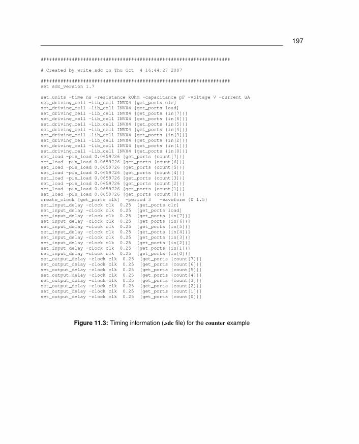
197
###################################################################
# Created by write_sdc on Thu Oct 4 16:44:27 2007
###################################################################set sdc_version 1.7
set_units -time ns -resistance kOhm -capacitance pF -voltage V -current uAset_driving_cell -lib_cell INVX4 [get_ports clr]set_driving_cell -lib_cell INVX4 [get_ports load]set_driving_cell -lib_cell INVX4 [get_ports {in[7]}]set_driving_cell -lib_cell INVX4 [get_ports {in[6]}]set_driving_cell -lib_cell INVX4 [get_ports {in[5]}]set_driving_cell -lib_cell INVX4 [get_ports {in[4]}]set_driving_cell -lib_cell INVX4 [get_ports {in[3]}]set_driving_cell -lib_cell INVX4 [get_ports {in[2]}]set_driving_cell -lib_cell INVX4 [get_ports {in[1]}]set_driving_cell -lib_cell INVX4 [get_ports {in[0]}]set_load -pin_load 0.0659726 [get_ports {count[7]}]set_load -pin_load 0.0659726 [get_ports {count[6]}]set_load -pin_load 0.0659726 [get_ports {count[5]}]set_load -pin_load 0.0659726 [get_ports {count[4]}]set_load -pin_load 0.0659726 [get_ports {count[3]}]set_load -pin_load 0.0659726 [get_ports {count[2]}]set_load -pin_load 0.0659726 [get_ports {count[1]}]set_load -pin_load 0.0659726 [get_ports {count[0]}]create_clock [get_ports clk] -period 3 -waveform {0 1.5}set_input_delay -clock clk 0.25 [get_ports clr]set_input_delay -clock clk 0.25 [get_ports load]set_input_delay -clock clk 0.25 [get_ports {in[7]}]set_input_delay -clock clk 0.25 [get_ports {in[6]}]set_input_delay -clock clk 0.25 [get_ports {in[5]}]set_input_delay -clock clk 0.25 [get_ports {in[4]}]set_input_delay -clock clk 0.25 [get_ports {in[3]}]set_input_delay -clock clk 0.25 [get_ports {in[2]}]set_input_delay -clock clk 0.25 [get_ports {in[1]}]set_input_delay -clock clk 0.25 [get_ports {in[0]}]set_output_delay -clock clk 0.25 [get_ports {count[7]}]set_output_delay -clock clk 0.25 [get_ports {count[6]}]set_output_delay -clock clk 0.25 [get_ports {count[5]}]set_output_delay -clock clk 0.25 [get_ports {count[4]}]set_output_delay -clock clk 0.25 [get_ports {count[3]}]set_output_delay -clock clk 0.25 [get_ports {count[2]}]set_output_delay -clock clk 0.25 [get_ports {count[1]}]set_output_delay -clock clk 0.25 [get_ports {count[0]}]
Figure 11.3: Timing information (.sdc file) for the counter example
198 CHAPTER 11: SOC Encounter Place and Route
(Copyright c©2006, 2010, Cadence Design Systems, Inc. All rights reserved worldwide. Reprinted with permission.)
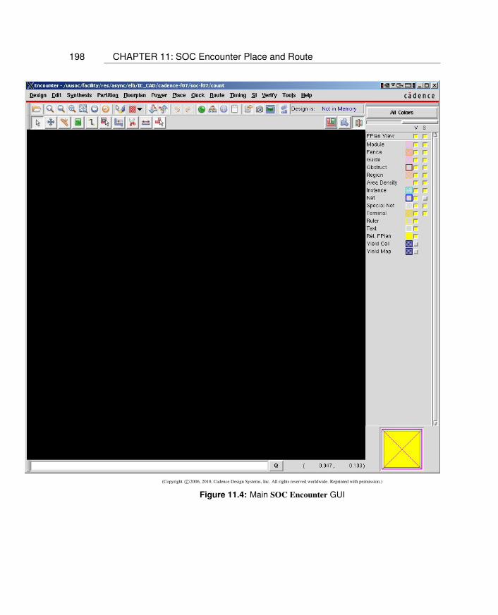
Figure 11.4: Main SOC Encounter GUI
199
(Copyright c©2006, 2010, Cadence Design Systems, Inc. All rights reserved worldwide. Reprinted with permission.)
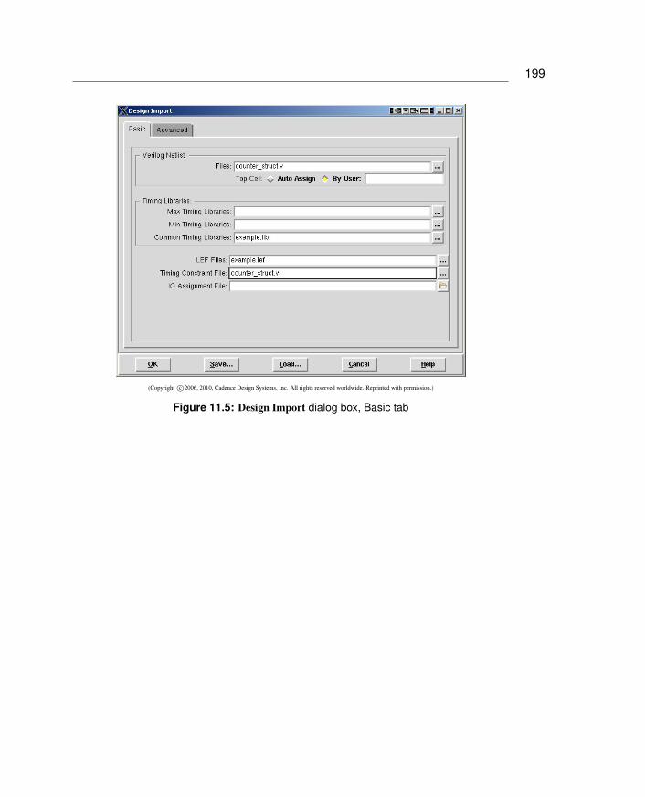
Figure 11.5: Design Import dialog box, Basic tab

200 CHAPTER 11: SOC Encounter Place and Route
(Copyright c©2006, 2010, Cadence Design Systems, Inc. All rights reserved worldwide. Reprinted with permission.)
Figure 11.6: Design Import IPO/CTS tab

201
(Copyright c©2006, 2010, Cadence Design Systems, Inc. All rights reserved worldwide. Reprinted with permission.)
Figure 11.7: Design Import Power tab
202 CHAPTER 11: SOC Encounter Place and Route
(Copyright c©2006, 2010, Cadence Design Systems, Inc. All rights reserved worldwide. Reprinted with permission.)
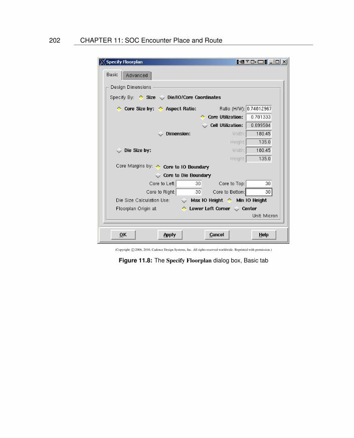
Figure 11.8: The Specify Floorplan dialog box, Basic tab

203
(Copyright c©2006, 2010, Cadence Design Systems, Inc. All rights reserved worldwide. Reprinted with permission.)
Figure 11.9: The Specify Floorplan dialog box, Advanced tab

204 CHAPTER 11: SOC Encounter Place and Route
(Copyright c©2006, 2010, Cadence Design Systems, Inc. All rights reserved worldwide. Reprinted with permission.)
Figure 11.10: Main design window after floorplanning

205
(Copyright c©2005, 2010, Cadence Design Systems, Inc. All rights reserved worldwide. Reprinted with permission.)
Figure 11.11: Dialog box for adding power and ground rings around your cell
206 CHAPTER 11: SOC Encounter Place and Route
(Copyright c©2006, 2010, Cadence Design Systems, Inc. All rights reserved worldwide. Reprinted with permission.)
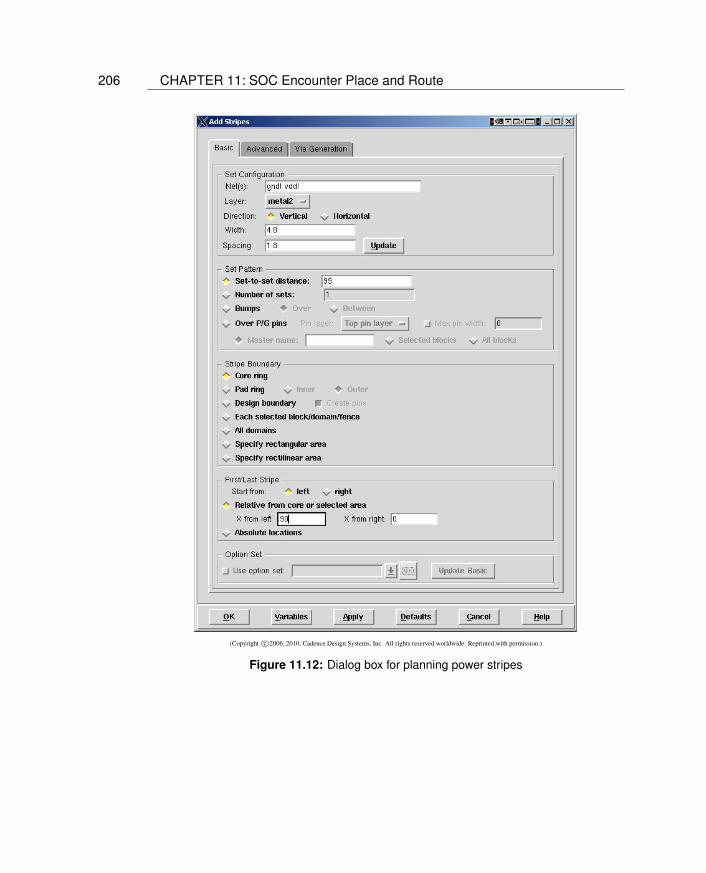
Figure 11.12: Dialog box for planning power stripes
207
(Copyright c©2006, 2010, Cadence Design Systems, Inc. All rights reserved worldwide. Reprinted with permission.)
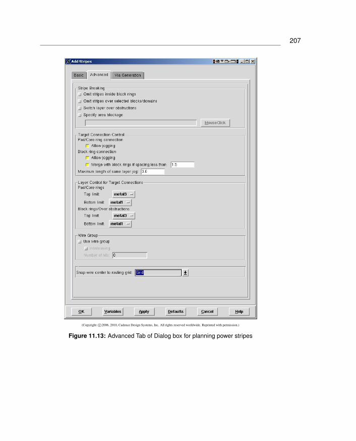
Figure 11.13: Advanced Tab of Dialog box for planning power stripes

208 CHAPTER 11: SOC Encounter Place and Route
(Copyright c©2006, 2010, Cadence Design Systems, Inc. All rights reserved worldwide. Reprinted with permission.)
Figure 11.14: Floorplan after power rings and stripes have been generated and connectedto the cell rows

209
(Copyright c©2006, 2010, Cadence Design Systems, Inc. All rights reserved worldwide. Reprinted with permission.)
Figure 11.15: Placement dialog box

210 CHAPTER 11: SOC Encounter Place and Route
(Copyright c©2006, 2010, Cadence Design Systems, Inc. All rights reserved worldwide. Reprinted with permission.)
Figure 11.16: View after placement of the cells

211
(Copyright c©2006, 2010, Cadence Design Systems, Inc. All rights reserved worldwide. Reprinted with permission.)
Figure 11.17: Dialog box for timing optimization

212 CHAPTER 11: SOC Encounter Place and Route
------------------------------------------------------------optDesign Final Summary
------------------------------------------------------------
+--------------------+---------+---------+---------+---------+---------+---------+| Setup mode | all | reg2reg | in2reg | reg2out | in2out | clkgate |+--------------------+---------+---------+---------+---------+---------+---------+| WNS (ns):| -0.329 | -0.329 | 0.981 | 0.681 | N/A | N/A || TNS (ns):| -1.138 | -1.138 | 0.000 | 0.000 | N/A | N/A || Violating Paths:| 5 | 5 | 0 | 0 | N/A | N/A || All Paths:| 24 | 8 | 16 | 8 | N/A | N/A |+--------------------+---------+---------+---------+---------+---------+---------+
Figure 11.18: Initial pre-CTS timing results
(Copyright c©2006, 2010, Cadence Design Systems, Inc. All rights reserved worldwide. Reprinted with permission.)
Figure 11.19: Generating a clock tree specification

213
(Copyright c©2006, 2010, Cadence Design Systems, Inc. All rights reserved worldwide. Reprinted with permission.)
Figure 11.20: Synthesize Clock Tree dialog box

214 CHAPTER 11: SOC Encounter Place and Route
(Copyright c©2006, 2010, Cadence Design Systems, Inc. All rights reserved worldwide. Reprinted with permission.)
Figure 11.21: Dialog box to display the clock tree

215
(Copyright c©2006, 2010, Cadence Design Systems, Inc. All rights reserved worldwide. Reprinted with permission.)
Figure 11.22: Design display showing the clock tree

216 CHAPTER 11: SOC Encounter Place and Route
------------------------------------------------------------optDesign Final Summary
------------------------------------------------------------
+--------------------+---------+---------+---------+---------+---------+---------+| Setup mode | all | reg2reg | in2reg | reg2out | in2out | clkgate |+--------------------+---------+---------+---------+---------+---------+---------+| WNS (ns):| -0.293 | -0.293 | 1.489 | 0.117 | N/A | N/A || TNS (ns):| -1.115 | -1.115 | 0.000 | 0.000 | N/A | N/A || Violating Paths:| 5 | 5 | 0 | 0 | N/A | N/A || All Paths:| 24 | 8 | 16 | 8 | N/A | N/A |+--------------------+---------+---------+---------+---------+---------+---------+
Figure 11.23: Timing results after the second (Post-CTS) optimization
(Copyright c©2006, 2010, Cadence Design Systems, Inc. All rights reserved worldwide. Reprinted with permission.)
Figure 11.24: NanoRoute dialog box
217
(Copyright c©2006, 2010, Cadence Design Systems, Inc. All rights reserved worldwide. Reprinted with permission.)
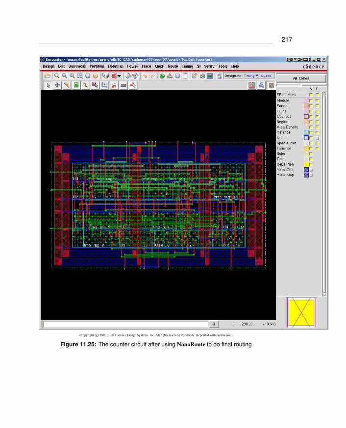
Figure 11.25: The counter circuit after using NanoRoute to do final routing

218 CHAPTER 11: SOC Encounter Place and Route
(Copyright c©2006, 2010, Cadence Design Systems, Inc. All rights reserved worldwide. Reprinted with permission.)
Figure 11.26: An error in pin placement after final routing

219
(Copyright c©2006, 2010, Cadence Design Systems, Inc. All rights reserved worldwide. Reprinted with permission.)
Figure 11.27: Design display after fixing the pin routing error
------------------------------------------------------------optDesign Final Summary
------------------------------------------------------------
+--------------------+---------+---------+---------+---------+---------+---------+| Setup mode | all | reg2reg | in2reg | reg2out | in2out | clkgate |+--------------------+---------+---------+---------+---------+---------+---------+| WNS (ns):| -0.338 | -0.338 | 1.445 | 0.339 | N/A | N/A || TNS (ns):| -1.327 | -1.327 | 0.000 | 0.000 | N/A | N/A || Violating Paths:| 5 | 5 | 0 | 0 | N/A | N/A || All Paths:| 24 | 8 | 16 | 8 | N/A | N/A |+--------------------+---------+---------+---------+---------+---------+---------+
Figure 11.28: Final post-route timing optimization results

220 CHAPTER 11: SOC Encounter Place and Route
(Copyright c©2006, 2010, Cadence Design Systems, Inc. All rights reserved worldwide. Reprinted with permission.)
Figure 11.29: Filler cell dialog box

221
(Copyright c©2006, 2010, Cadence Design Systems, Inc. All rights reserved worldwide. Reprinted with permission.)
Figure 11.30: Final cell layout after filler cells are added

222 CHAPTER 11: SOC Encounter Place and Route
(Copyright c©2006, 2010, Cadence Design Systems, Inc. All rights reserved worldwide. Reprinted with permission.)
Figure 11.31: A zoomed view of a final routed cell

223
(Copyright c©2006, 2010, Cadence Design Systems, Inc. All rights reserved worldwide. Reprinted with permission.)
Figure 11.32: Dialog box for verifying connectivity
224 CHAPTER 11: SOC Encounter Place and Route
(Copyright c©2006, 2010, Cadence Design Systems, Inc. All rights reserved worldwide. Reprinted with permission.)
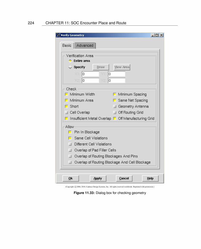
Figure 11.33: Dialog box for checking geometry

225
(Copyright c©2006, 2010, Cadence Design Systems, Inc. All rights reserved worldwide. Reprinted with permission.)
Figure 11.34: Dialog box for exporting DEF
226 CHAPTER 11: SOC Encounter Place and Route
(Copyright c©2006, 2010, Cadence Design Systems, Inc. All rights reserved worldwide. Reprinted with permission.)
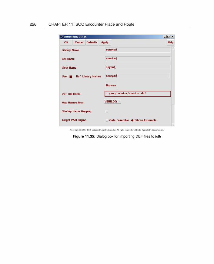
Figure 11.35: Dialog box for importing DEF files to icfb

227
(Copyright c©2006, 2010, Cadence Design Systems, Inc. All rights reserved worldwide. Reprinted with permission.)
Figure 11.36: Search dialog box for finding all the cell abstracts
228 CHAPTER 11: SOC Encounter Place and Route
(Copyright c©2006, 2010, Cadence Design Systems, Inc. All rights reserved worldwide. Reprinted with permission.)
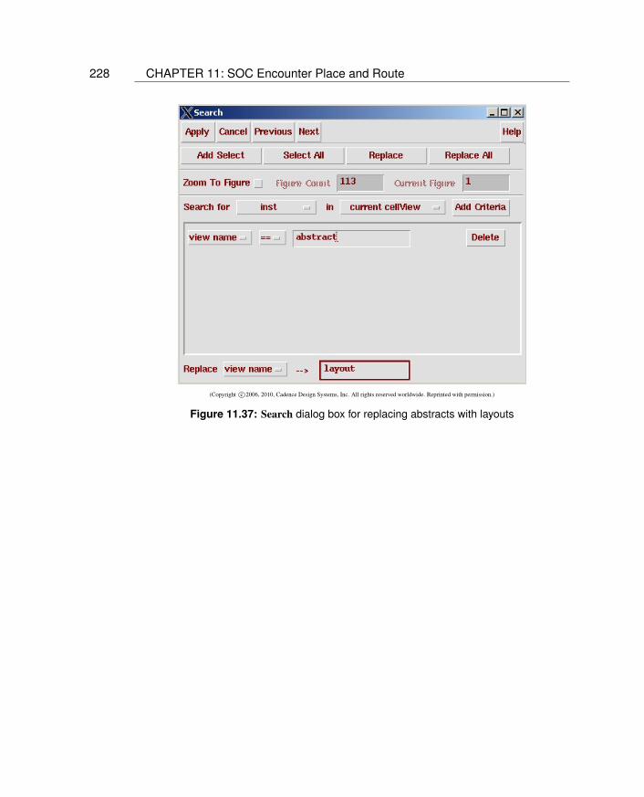
Figure 11.37: Search dialog box for replacing abstracts with layouts

229
(Copyright c©2006, 2010, Cadence Design Systems, Inc. All rights reserved worldwide. Reprinted with permission.)
Figure 11.38: Dialog box for importing structural Verilog into a new schematic view
230 CHAPTER 11: SOC Encounter Place and Route
(Copyright c©2006, 2010, Cadence Design Systems, Inc. All rights reserved worldwide. Reprinted with permission.)
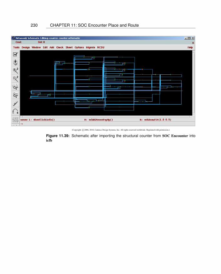
Figure 11.39: Schematic after importing the structural counter from SOC Encounter intoicfb
231
(Copyright c©2006, 2010, Cadence Design Systems, Inc. All rights reserved worldwide. Reprinted with permission.)
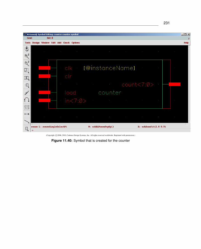
Figure 11.40: Symbol that is created for the counter

232 CHAPTER 11: SOC Encounter Place and Route
################################################# Encounter Input configuration file ## Erik Brunvand, University of Utah #################################################global rda_Input########################################################### Here are the parts you need to update for your design########################################################### Your input is structural verilog. Set the top module name# and also give the .sdc file you used in synthesis for the# clock timing constraints. Also an io file if used.set rda_Input(ui_netlist) {counter_struct.v}set rda_Input(ui_topcell) {counter}set rda_Input(ui_timingcon_file) {counter_struct.sdc}set rda_Input(ui_io_file) {}## Leave min and max empty if you have only one timing library# (space-separated if you have more than one)set rda_Input(ui_timelib) {example.lib}set rda_Input(ui_timelib,min) {}set rda_Input(ui_timelib,max) {}## Set the name of your lef file(s) (space-separated if more than one).set rda_Input(ui_leffile) {example.lef}## Include the footprints of your cells that fit these uses. Delay# can be an inverter or a buffer. Leave buf blank if you don’t# have a non-inverting buffer. These are the "footprints" in# the .lib file, not the cell names.set rda_Input(ui_buf_footprint) {}set rda_Input(ui_delay_footprint) {inv}set rda_Input(ui_inv_footprint) {inv}set rda_Input(ui_cts_cell_footprint) {inv}## You might want to set core utilization and core_to spacingset rda_Input(ui_core_util) {0.7}set rda_Input(ui_core_to_left) {30.0}set rda_Input(ui_core_to_right) {30.0}set rda_Input(ui_core_to_top) {30.0}set rda_Input(ui_core_to_bottom) {30.0}########################################################### Below here you should be able leave alone...##########################################################... For remaining lines, see Appendix ...
Figure 11.41: Configuration file for reading in the counter example
233
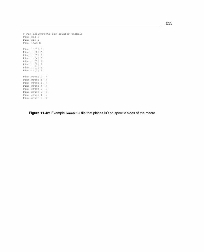
# Pin assignments for counter examplePin: clk EPin: clr EPin: load E
Pin: in[7] SPin: in[6] SPin: in[5] SPin: in[4] SPin: in[3] SPin: in[2] SPin: in[1] SPin: in[0] S
Pin: count[7] NPin: count[6] NPin: count[5] NPin: count[4] NPin: count[3] NPin: count[2] NPin: count[1] NPin: count[0] N
Figure 11.42: Example counter.io file that places I/O on specific sides of the macro
234 CHAPTER 11: SOC Encounter Place and Route
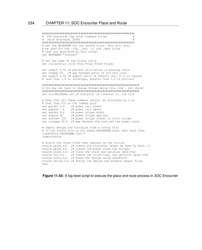
########################################################### SOC Encounter Top-level Command script ## (Erik Brunvand, 2008) ############################################################ set the BASENAME for the config files. This will also# be used for the .lib, .lef, .v, and .spef files# that are generated by this scriptset BASENAME "counter"
# set the name of the filler cellsset fillerCells [list FILL FILL2 FILL4 FILL8]
set usepct 0.70 ;# percent utilization in placing cellsset rowgap 18 ;# gap between pairs of std cell rowsset aspect 0.50 ;# aspect ratio of overall cell (1.0 is square)# less than 1.0 is landscape, greater than 1.0 is portrait
############################################################## You may not have to change things below this line - but check!#############################################################set clockBufName inv ;# Footprint of inverter in .lib file
# Note that all these numbers should be divisible by 3 so# that they fit on the lambda gridset pwidth 9.9 ;# power rail widthset pspace 1.8 ;# power rail spaceset swidth 4.8 ;# power stripe widthset sspace 99 ;# power stripe spacingset soffset 120 ;# power stripe offset to first stripeset coregap 30.0 ;# gap between the core and the power rails
# Import design and floorplan from a config file# If the config file is not named $BASENAME.conf, edit this line.loadConfig $BASENAME.conf 0commitConfig
# source the other files that operate on the circuitsource fplan.tcl ;# create the floorplan (might be done by hand...)source pplan.tcl ;# create the power rings and stripessource place.tcl ;# Place the cells and optimize (pre-CTS)source cts.tcl ;# Create the clock tree, and optimize (post-CTS)source route.tcl ;# Route the design using nanoRoutesource verify.tcl ;# Verify the design and produce output filesexit
Figure 11.43: A top-level script to execute the place and route process in SOC Encounter