characterisation and modelling of graphene fets for...
TRANSCRIPT

Thesis for The Degree of Doctor of Philosophy
Characterisation and Modelling of Graphene FETs forTerahertz Mixers and Detectors
Michael Andersson
Terahertz and Millimetre Wave LaboratoryDepartment of Microtechnology and Nanoscience - MC2
Chalmers University of TechnologyGoteborg, Sweden, 2016

Characterisation and Modelling of Graphene FETs for TerahertzMixers and Detectors
Michael Andersson
© Michael Andersson, 2016
ISBN 978-91-7597-453-8
Doktorsavhandlingar vid Chalmers tekniska hogskolaNy serie nr 4134ISSN 0346-718X
Technical report MC2-342ISSN 1652-0769
Terahertz and Millimetre Wave LaboratoryDepartment of Microtechnology and Nanoscience - MC2Chalmers University of TechnologySE-412 96 Goteborg, SwedenPhone: +46 (0) 31 772 1000
Cover: From left side to right side, agreement of the Volterra FET powerdetector model to measured GFET NEP, a micrograph of a 600 GHz antenna-integrated direct detector with an SEM image of the GFET and a micrographof a 200 GHz integrated CPW mixer with an SEM image of the GFET.
Printed by Chalmers ReproserviceGoteborg, Sweden, August 2016

Till min familj

iv

Abstract
Graphene is a two-dimensional sheet of carbon atoms with numerous envisagedapplications owing to its exciting properties. In particular, ultrahigh-speedgraphene field effect transistors (GFETs) are possible due to the unprecedentedcarrier velocities in ideal graphene. Thus, GFETs may potentially advance thecurrent upper operation frequency limit of RF electronics.
In this thesis, the practical viability of high-frequency GFETs based onlarge-area graphene from chemical vapour deposition (CVD) is investigated.Device-level GFET model parameters are extracted to identify performancebottlenecks. Passive mixer and power detector terahertz circuits operatingabove the present active GFET transit time limit are demonstrated.
The first device-level microwave noise characterisation of a CVD GFETis presented. This allows for the de-embedding of the noise parameters andconstruction of noise models for the intrinsic device. The correlation of thegate and drain noise in the PRC model is comparable to that of Si MOSFETs.This indicates higher long-term GFET noise relative to HEMTs.
An analytical power detector model derived using Volterra analysis on theFET large-signal model is verified at frequencies up to 67 GHz. The draincurrent derivatives, intrinsic capacitors and parasitic resistors of the closed-form expressions for the noise equivalent power (NEP) are extracted from DCand S-parameter measurements. The model shows that a short gate lengthand a bandgap in the channel are required for optimal FET sensitivity.
A power detector integrated with a split bow-tie antenna on a Si substratedemonstrates an optical NEP of 500 pW/Hz1/2 at 600 GHz. This representsa state-of-the-art result for quasi-optically coupled, rectifying direct detectorsbased on GFETs operating at room temperature.
The subharmonic GFET mixer utilising the electron-hole symmetry ingraphene is scaled to operate with a centre frequency of 200 GHz, the highestfrequency reported so far for graphene integrated circuits. The down-convertercircuit is implemented in a coplanar waveguide (CPW) on Si and exhibits aconversion loss (CL) of 29 ± 2 dB in the 185-210 GHz band.
In conclusion, the CVD GFETs in this thesis are unlikely to reach theperformance required for high-end RF applications. Instead, they currentlyappear more likely to compete in niche applications such as flexible electronics.
Keywords: Field-effect transistors (FETs), graphene, integrated circuits,microwave amplifiers, millimetre and submillimetre waves, nanofabrication,noise modelling, nonlinear device modelling, power detectors, subharmonicresistive mixers, terahertz detectors, Volterra.
v

vi
List of publications
Appended papers
This thesis is based on the following papers:
[A] M. Andersson and J. Stake, “An Accurate Empirical Model Basedon Volterra Series for FET Power Detectors,” in IEEE Transactions onMicrowave Theory and Techniques, vol. 64, no. 5, pp. 1431-1441, May2016. DOI: 10.1109/TMTT.2016.2532326
[B] A. Zak,M. Andersson, M. Bauer, J. Matukas, A. Lisauskas, H. G. Roskos,and J. Stake, “Antenna-Integrated 0.6 THz FET Direct Detectors Basedon CVD graphene,” in Nano Letters, vol. 14, no. 10, pp. 5834-5838,September 2014. DOI: 10.1021/nl5027309
[C] M. Andersson, Y. Zhang, and J. Stake, “A 185-215 GHz SubharmonicResistive Graphene FET Integrated Mixer on Silicon,” submitted toIEEE Transactions on Microwave Theory and Techniques, July 2016.
[D] M. Andersson, O. Habibpour, J. Vukusic, and J. Stake, “ResistiveGraphene FET Subharmonic Mixers: Noise and Linearity Assessment,”in IEEE Transactions on Microwave Theory and Techniques, vol. 60, no.12, pp. 4035-4042, December 2012. DOI: 10.1109/TMTT.2012.2221141
[E] M. Andersson, O. Habibpour, J. Vukusic, and J. Stake, “10 dB small-signal graphene FET amplifier,” in Electronics Letters, vol. 48, no. 14,pp. 861-863, July 2012. DOI: 10.1049/el.2012.1347
[F] M. Tanzid, M. Andersson, J. Sun, and J. Stake, “Microwave noisecharacterization of graphene field effect transistors,” in Applied PhysicsLetters, vol. 104, no. 1, pp. 013502-1−013502-4, January 2014. DOI:10.1063/1.4861115
[G] M. Andersson, A. Vorobiev, J. Sun, A. Yurgens, S. Gevorgian, andJ. Stake, “Microwave characterization of Ti/Au-graphene contacts,” inApplied Physics Letters, vol. 103, no. 17, pp. 173111-1−173111-4, Oc-tober 2013. DOI: 10.1063/1.4826645
[H] S. Bidmeshkipour, A. Vorobiev, M. Andersson, A. Kompany, andJ. Stake “Effect of ferroelectric substrate on carrier mobility in graphenefield-effect transistors,” in Applied Physics Letters, vol. 107, no. 17, pp.173106-1−173106-5, October 2015. DOI: 10.1063/1.4934696
vii

viii
[I] M. Andersson, A. Ozcelikkale, M. Johansson, U. Engstrom, A. Voro-biev, and J. Stake, “Feasibility of Ambient RF Energy Harvesting forSelf-Sustainable M2M Communications Using Transparent and FlexibleGraphene Antennas,” accepted for publication in IEEE Access, August2016.
Other papers and publications
The following papers and publications are not appended to the thesis, eitherdue to contents overlapping with appended papers, or due to contents notrelated to the thesis.
[a] Y. Zhang, M. Andersson, and J. Stake, “A 200 GHz Graphene FETResistive Subharmonic Mixer,” in IEEE MTT-S International MicrowaveSymposium (IMS) Digest, San Fransisco, USA, 2016. DOI:10.1109/MWSYM.2016.7540287
[b] A. Generalov, M. Andersson, X. Yang, and J. Stake, “Optimizationof THz graphene FET detector integrated with a bowtie antenna,” 10thEuropean Conference on Antennas and Propagation (EuCAP), Davos,Switzerland, 2016. DOI: 10.1109/EuCAP.2016.7481475
[c] M. Bauer, A. Lisauskas, A. Zak, M. Andersson, J. Stake, J. Matukas,and H. Roskos, “Terahertz detection with graphene field-effect transis-tors,” Graphene Week 2015, Manchester, United Kingdom, 2015.
[d] M. Bauer, M. Andersson, A. Zak, P. Sakalas, D. Cibiraite A. Lisauskas,M. Schroter, J. Stake, and H. Roskos, “The potential of sensitivity en-hancement by the thermoelectric effect in carbon-nanotube and grapheneTera-FETs,” 19th International Conference on Electron Dynamics inSemiconductors, Optoelectronics and Nanostructures (EDISON’19), Sala-manca, Spain, 2015. DOI: 10.1088/1742-6596/647/1/012004
[e] M. Andersson, A. Vorobiev, S. Gevorgian, and J. Stake, “Extraction ofcarrier transport properties in graphene from microwave measurements,”European Microwave Conference (EuMC) 2014, Rome, Italy, 2014.DOI: 10.1109/EuMC.2014.6986444
[f] M. Andersson, A. Vorobiev, S. Gevorgian, and J. Stake, “Comparisonof carrier scattering mechanisms in chemical vapor deposited grapheneon fused silica and strontium titanite substrates,” Graphene Week 2014,Goteborg, Sweden, 2014.
[g] A. Zak, M. Andersson, M. Bauer, A. Lisauskas, H. Roskos, and J. St-ake, “20 μm gate width CVD graphene FETs for 0.6 THz detection,”39th IEEE International Conference on Infrared, Millimeter and Tera-hertz Waves, Tucson, Arizona, 2014. DOI:10.1109/IRMMW-THz.2014.6956250

ix
[h] M. Andersson, A. Vorobiev, J. Sun, A. Yurgens, and J. Stake, “To-wards Graphene Electrodes for High Performance Acoustic Resonators,”in 37th Workshop on Compound Semiconductor Devices and IntegratedCircuits held in Europe (WOCSDICE), Warnemunde, Germany, 2013.
[i] M. Andersson, O. Habibpour, J. Vukusic, and J. Stake, “Noise FigureCharacterization of a Subharmonic Graphene FET mixer,” in IEEEMTT-S International Microwave Symposium (IMS) Digest, Montreal,Canada, 2012. DOI: 10.1109/MWSYM.2012.6259519
[j] M. Andersson, O. Habibpour, J. Vukusic, and J. Stake, “TowardsPractical Graphene Field Effect Transistors for Microwaves,” in Giga-Hertz Symposium, Stockholm, Sweden, 2012.

x

Acronyms
2DEG Two-Dimensional Electron Gas. 1, 8
Al2O3 Aluminium Oxide. 8, 18, 21, 27
ALD Atomic Layer Deposition. 18, 21
CAD Computer-Aided Design. 38
CL Conversion Loss. 34, 42
CMOS Complementary Metal-Oxide-Semiconductor. 2, 15, 30, 31, 43, 47,49, 53
CNT Carbon NanoTube. 2
CPW CoPlanar Waveguide. 38, 43–45
CVD Chemical Vapour Deposition. 3, 12–16, 19–22, 25, 30, 31, 37, 39, 41,51, 53, 54
DOS Density of States. 8, 19
EM ElectroMagnetic. 40
FET Field-Effect Transistor. 1–3, 5, 6, 9, 11, 18, 19, 22–28, 30–34, 40–43,47–49, 53, 54
GaAs Gallium Arsenide. 1, 7, 8, 22, 30, 31, 37, 42, 43
GaN Gallium Nitride. 7, 42
GFET Graphene Field-Effect Transistor. 2, 3, 5, 9, 11, 12, 17–31, 33, 34,39–46, 49, 50, 53, 54
h-BN Hexagonal Boron Nitride. 2, 8, 10, 13, 14, 16, 54
HEMT High Electron Mobility Transistor. 1, 2, 19, 22, 25, 26, 29–31, 37, 43,49, 54
IF Intermediate Frequency. 3, 34, 37, 42
xi

xii Acronyms
IIP3 Input Third-Order Intercept Point. 42
IM3 Third-Order Intermodulation. 34, 35
InAs Indium Arsenide. 2, 7
InP Indium Phosphide. 1, 2, 22, 29, 31, 37
LiNbO3 Lithium Niobium Oxide. 11
LNA Low-Noise Amplifier. 1, 30, 37, 54
LO Local Oscillator. 3, 32, 34, 35, 42, 43, 45, 53
M2M Machine-to-Machine. 50, 51
MAG Maximum Available Gain. 25
MESFET Metal-Semiconductor Field-Effect Transistor. 1
MMIC Monolithic Microwave Integrated Circuit. 1, 37
MOSFET Metal-Oxide-Semiconductor Field-Effect Transistor. 3, 30, 31, 54
NEP Noise Equivalent Power. 32, 34, 47, 49, 50, 53
NF Noise Figure. 26, 28, 41
NW NanoWire. 2
PMMA Poly(Methyl MethAcrylate). 14, 17, 22
RF Radio Frequency. 15, 17, 18, 22, 32, 34, 37, 42, 43, 45, 47, 48, 50, 51, 53,54
SEM Scanning Electron Microscope. 14, 20
SiC Silicon Carbide. 11, 14–16, 22, 26, 30, 31, 40, 41, 54
SiO2 Silicon Dioxide. 8–12, 14, 16, 18, 20, 30
THz Terahertz. 1–3, 37, 46, 49, 53
TLM Transmission Line Method. 20, 21, 23, 26

Notations
βv Detector voltage responsivity. 32, 33, 48
ΓS Source reflection coefficient. 28, 39, 40
Δf Noise bandwidth. 27
ε Dielectric permittivity. 10
μ Carrier mobility. 7, 9, 10, 21
ρ Electrical resistivity. 7, 10, 25
σ Electrical conductivity. 7–9
C Gate-drain noise correlation coefficient. 27–30
Cgd Intrinsic gate-drain capacitance. 24–28, 32, 33, 48
Cgs Intrinsic gate-source capacitance. 24–26, 32, 33, 48
E Electric field. 9, 10
E Energy. 5, 6, 8, 10
EF Fermi energy. 6, 8
Eg Energy bandgap. 7, 11
GT Transducer power gain. 39
Ids Drain-source DC current. 22, 25, 28–31, 33, 34, 54
Lg Gate length. 9, 23–26, 28–31, 39, 48, 49
NFmin Minimum noise figure of a two-port. 26, 28, 41
P PRC drain noise coefficient. 27–29
R PRC gate noise coefficient. 27–29
RD Parasitic drain resistance. 9, 19, 23–26, 33, 48
RG Parasitic gate resistance. 23–26, 30, 31
RS Parasitic source resistance. 9, 19, 23–26, 30, 31, 33, 48
xiii

xiv Notations
Rn Noise resistance. 26, 28
Rsh Sheet resistance. 19–22, 50
SBA Ambient RF intensity to harvest. 50
Td Equivalent drain noise temperature. 26–29, 41
Tg Equivalent gate noise temperature. 26–29, 41
Tmin Minimum noise temperature of a two-port. 26, 29
Tn Equivalent input noise temperature. 26, 28, 41
U Mason’s unilateral gain. 23–25
VDirac Gate voltage of the Dirac point. 9, 34, 35
Wg Gate width. 9, 19, 24–26, 31, 39, 48
Y Electrical admittance. 26
Z Electrical impedance. 44
Z0 Transmission line characteristic impedance. 22, 26, 33, 47, 48
e2 Noise voltage. 27
f Frequency. 26, 27, 29, 32, 43, 47, 48
fmax Maximum frequency of oscillation. 1, 2, 23–26, 29, 31, 37, 39, 41
fT Cutoff frequency. 1, 2, 23–26, 30, 31, 39
gme Extrinsic (DC) transconductance. 22, 25, 30, 31
gmi Intrinsic (small-signal) transconductance. 24, 25, 28, 31
h21 Short circuit current gain. 23
� Planck’s constant. 6, 8, 11
i2d Drain noise current. 27, 28
i2g Gate noise current. 27, 28
kB Boltzmann’s constant. 8, 10, 11, 27, 28
n Total carrier concentration. 7–11, 21
n0 Residual carrier concentration. 8, 21
nth Thermally generated carrier concentration. 8, 10
q Electron charge. 7, 9, 21, 27
vF Fermi velocity. 6, 8, 11
vsat Carrier saturation velocity. 10, 11

Contents
Abstract v
List of publications vii
Acronyms xi
Notations xiii
1 Introduction 11.1 Thesis outline . . . . . . . . . . . . . . . . . . . . . . . . . . . . 3
2 Graphene properties for high-speed electronics 52.1 Graphene band structure . . . . . . . . . . . . . . . . . . . . . 52.2 Carrier transport in graphene . . . . . . . . . . . . . . . . . . . 6
2.2.1 Gate-induced versus residual carrier concentration . . . 82.2.2 Extraction of the low-field mobility . . . . . . . . . . . . 92.2.3 Limitations on the low-field mobility in graphene . . . . 92.2.4 High-field carrier velocities in graphene . . . . . . . . . 102.2.5 Opening a bandgap in graphene . . . . . . . . . . . . . 11
2.3 Practical status of graphene synthesis . . . . . . . . . . . . . . 122.3.1 Exfoliation from highly ordered graphite . . . . . . . . . 122.3.2 Graphene and h-BN synthesis by CVD . . . . . . . . . . 122.3.3 Transfer of CVD materials to insulating substrates . . . 142.3.4 Sublimation and CVD growth on SiC . . . . . . . . . . 142.3.5 Which type of graphene and why? . . . . . . . . . . . . 15
3 Fabrication, device-level characterisation and modelling of GFETs 173.1 Device fabrication . . . . . . . . . . . . . . . . . . . . . . . . . 173.2 DC characterisation of GFETs . . . . . . . . . . . . . . . . . . 18
3.2.1 Ohmic contacts to graphene . . . . . . . . . . . . . . . . 193.2.2 Channel mobility and sheet resistance . . . . . . . . . . 213.2.3 Transconductance and output conductance . . . . . . . 22
3.3 Small-signal equivalent FET circuit . . . . . . . . . . . . . . . . 233.4 Graphene for active microwave FETs . . . . . . . . . . . . . . . 23
3.4.1 Figures of merit for active FET two-ports . . . . . . . . 233.4.2 Benchmark of state-of-the-art active GFETs . . . . . . 25
3.5 Quantifying the GFET noise performance . . . . . . . . . . . . 263.5.1 Noise modelling of FETs . . . . . . . . . . . . . . . . . . 27
xv

xvi Contents
3.5.2 Construction of a GFET noise model . . . . . . . . . . . 283.5.3 Prospects for GFET low-noise amplifiers . . . . . . . . . 29
3.6 Large-signal equivalent FET circuit . . . . . . . . . . . . . . . . 313.7 Nonlinear circuit applications of GFETs . . . . . . . . . . . . . 31
3.7.1 Volterra analysis of FET power detectors . . . . . . . . 323.7.2 Operation principle of resistive mixers . . . . . . . . . . 34
4 High-frequency circuits based on GFETs 354.1 Integrated microwave circuits . . . . . . . . . . . . . . . . . . . 35
4.1.1 Planar transmission lines . . . . . . . . . . . . . . . . . 364.2 Small-signal GFET amplifiers . . . . . . . . . . . . . . . . . . . 37
4.2.1 Matching circuit design and performance . . . . . . . . 384.2.2 Analysis of the amplifier noise figure . . . . . . . . . . . 39
4.3 Frequency mixers based on GFETs . . . . . . . . . . . . . . . . 404.3.1 Fundamental mixers . . . . . . . . . . . . . . . . . . . . 404.3.2 Subharmonic mixers . . . . . . . . . . . . . . . . . . . . 41
4.4 Quasi-optical THz circuits . . . . . . . . . . . . . . . . . . . . . 444.5 Electrical model for FET THz detectors . . . . . . . . . . . . . 45
4.5.1 Frequency dependence of the NEP . . . . . . . . . . . . 464.5.2 Design and characterisation of GFET detectors . . . . . 46
4.6 Graphene antennas for energy harvesting . . . . . . . . . . . . 48
5 Conclusions and future outlook 51
6 Summary of appended papers 53
A Recipe CVD GFET circuits 57
Acknowledgments 61
Bibliography 63
Appended Papers 77

Chapter 1
Introduction
High-frequency electromagnetic waves in the microwave (300 MHz to 100 GHz)and terahertz (loosely defined as 100 GHz to 10 THz) frequency regions of thespectrum are used in numerous applications. Wireless technology that operatesin the lower-GHz range is a defining factor of life today as an enabler of therapidly increasing flow of data exchanged in modern society. In the THzregime, historically niche applications in spectroscopy, earth remote sensingand radio astronomy are dominating [1]. Nevertheless, more recently, interestand practical implementation of THz in fields closer to everyday life, includingsecurity and surveillance [2], medicine and disease diagnostics [3], and futurehigh-speed communication networks [4] have emerged.
Today, the lack of compact, room-temperature and affordable sources andtransmitters, detectors and receivers hinders the full utilisation of the greatpotential of THz waves. Attempts to bridge this so-called THz gap have beeninitiated both by increasing in frequency from the electronics side [5] and by de-creasing in frequency from the photonics side [6]. In solid-state technology, theSchottky diode is the longtime workhorse for THz electronics [7]. Importantly,the noise of high spectral resolution and diode-based heterodyne receivers hasa fundamental limit given by the conversion loss of the down-converting mixer.
An active receiver designed with field-effect transistors (FETs) permitsboth potentially lower noise and a higher circuit integration level. Presently,FETs are used in THz receivers to feed power to diode multiplier chains andfor intermediate frequency low-noise amplifiers (LNAs). Vast progress hasbeen achieved since the demonstration of the first microwave GaAs MESFETin 1967 [8] and the advent of the GaAs monolithic microwave integrated cir-cuit (MMIC) technology during the 1970s [9]. Subsequently, the strategy toachieve higher frequencies has been to scale to the shortest transistor channelspossible and use channel materials with the highest possible carrier velocities.A milestone was the introduction of the GaAs high electron mobility transistor(HEMT) [10]. The HEMT utilises a 2DEG channel to separate the carriersfrom the impurity dopants. Currently, the leading FET technology is the InPHEMT with maximum frequency of oscillation fmax = 1.5 THz [11] and cutofffrequency fT = 688 GHz [12]. This allows for the of design small-signal InPHEMT amplifiers above 1 THz [11]. In addition, passive FET detectors areused in low-spectral-resolution, incoherent receivers at several THz [13].
1

2 Chapter 1. Introduction
a) b)
10
100
1000
0.01 0.1 1
Gate length (μm)
Cu
toff
fre
qu
en
cy (
GH
z)
Exoliated GFET
Epitaxial GFET
CVD GFET
InGaAs NW FET
CNT FET
InP HEMT & GaAs mHEMT
GaAs pHEMT
Si MOSFET
Gate length (μm)
f ma
x (
GH
z)
GFET
InGaAs NW FET
InP HEMT & GaAs mHEMT
GaAs pHEMT
Si MOSFET
0.01 0.1 1
10
100
1000
1
1.5 THz
420 GHz
137 GHz
290 GHz
312 GHz280 GHz
688 GHz
485 GHz427 GHz
400 GHz300 GHz
152 GHz 153 GHz
Fig. 1.1: State-of-the-art de-embedded a) fT and b) fmax for HEMTs, Si CMOS,CNT [11,17] and NW FETs [15,16] against reported intrinsic GFETs [11,17–21].
However, as shown in Fig. 1.1 the InP HEMT has seemingly reached itsperformance limits in terms of gate length scaling. Moreover, the modernIII-V epitaxy enables the growth of pure InAs channels on InP substratesto maximise the carrier velocity. Furthermore, InP HEMT is an expensiveand low-yield technology. Consequently, researchers constantly scrutinise newdevice layouts and new candidate materials with potentially higher carriervelocities for FETs to reach further into the THz range. In this context,semiconducting carbon nanotubes (CNTs) [14] and wrap-around gated InAsnanowires (NWs) [15,16] are explored. To date, they are not competitive withthe state-of-the-art technologies in Fig. 1.1 for high-frequency transistors.
In this thesis, the intrinsically high-mobility carbon material graphene [22]is studied for use in high-frequency FETs. Graphene belongs to a group oftwo-dimensional materials attracting significant attention for electronics dueto their distinctive and diverse properties [23]. The toolbox contains zero-bandgap materials (graphene, silicene and germanene), semiconductors (MoS2and black phosphorous) and insulators (boron nitride). Potential applicationsfor these materials are found based both on their individual attributes and bythe utility enabled when stacked in heterostructures [24]. Notably, graphenealone exhibits a set of qualities that open new possibilities. The electricalconductivity together with bendability and transparency is advantageous fortouchscreens and transparent electrodes [25]. The low ratio of volume to areacombined with the field effect is favourable for sensors [26]. The outstandingmobility and mechanical flexibility make graphene a potential platform for thenext generation of high-speed transistors [17] and ubiquitous electronics [27].
The state-of-the-art high-frequency GFETs are summarised in Fig. 1.1.Judging from the record intrinsic cutoff frequency fT = 427 GHz [18], graphenehas an edge over CNTs and NWs and is even comparable to III-V HEMTs. Inthe absence of a bandgap, the poor current saturation in GFETs results in lowfmax values. Moreover, there is an alarming discrepancy in the extrinsic values,which include the parasitics and are limited to <50 GHz [19, 21]. The carriermobility in GFETs is currently greatly impeded by the oxides sandwichinggraphene. This may be solved by sandwiching graphene in hexagonal boronnitride (h-BN) [28]. However, there is presently no in situ growth method forwafer-scale h-BN/graphene/h-BN heterostructures.

1.1. Thesis outline 3
Antenna
Bandpass
filter
Low-noise
RF amplifierMixer IF filter IF amplifier
Power
detector
Data
Local
oscillator
Fig. 1.2: The block diagram of a typical heterodyne receiver. The mixer is notpresent in an incoherent receiver, resulting in lower spectral resolution.
An essential objective of this thesis work was to advance the wafer-scaleGFET technology. Consequently, a fabrication process for GFETs on graphenegrown by chemical vapour deposition (CVD) on copper foils and transferred tosilicon substrates [29] was developed. The process presented in this thesis canbe transferred to full wafer-scale [30] and potentially to flexible substrates [27].The main contributions to the field of graphene high-frequency electronics aredivided into two categories. First, the extraction of models to perceive currentand fundamental problems for GFETs is described. Second, the fabrication ofcircuit demonstrators towards a GFET THz detector focal-plane array [31] anda GFET-based millimetre wave heterodyne receiver is described (Fig. 1.2).
The model highlight is the verification of analytical expressions for the FETpower detector figures of merit based on a Volterra analysis of the nonlinearFET equivalent circuit [Paper A]. The missing bandgap, rather than the lowmobility, is implied to be the major obstacle for higher GFET sensitivity.
Moreover, noise models of active microwave GFETs for small-signal IFamplifiers are extracted to establish a first indication of the long-term prospectsof the GFET noise performance [Paper F]. The noise correlation factor andthe gate length normalised noise figure are comparable with Si MOSFETs.Future studies will establish whether higher-quality gate stacks improve thecorrelation or if it is fundamental to the device structure.
The demonstrator highlights are the subharmonic GFET mixer scaled toa record frequency of 200 GHz for integrated graphene circuits [Paper C] andthe quasi-optical GFET detector with record sensitivity at 600 GHz [Paper B].The subharmonic mixer operation is inherent in graphene due to the symmetryof electron and hole carriers [32] and is advantageous at millimetre waves toallow a lower frequency for the high-power local oscillator (LO) source.
1.1 Thesis outline
The thesis chapters introduce graphene and microwave technology in a widercontext to set the scene for the appended papers. Chapter 2 compares therelevant theoretical electronic properties of graphene to the current practicalstatus of graphene synthesis. Chapter 3 describes the figures of merit andmethods of characterisation and modelling for active and passive microwaveand THz GFETs. Chapter 4 presents the technological background for theintegrated GFET circuit demonstrators. Chapter 5 finally draws summarisingconclusions out of which future work directions are identified.

4 Chapter 1. Introduction

Chapter 2
Graphene properties forhigh-speed electronics
Fast microwave FETs are core building blocks, i.e., in high-speed communica-tion networks. To realise such a device, the carrier transit time under the gatemust be short. This necessitates a short gate length transistor and a channelmaterial with the highest possible carrier velocity. This chapter presents thetheoretical potential and practical limitations of graphene in this context tounderstand the current performance and future improvements of GFETs.
2.1 Graphene band structure
Graphene consists of a monolayer of carbon atoms in a hexagonal lattice, con-nected via sp2-hybridisation, as shown in Fig. 2.1a). In graphene, each atomhas three neighbours connected by strong covalent, in-plane σ-bonds. Whereasthese electrons are localised, defining the carbon-carbon binding distance ofaC−C = 1.42 A, the remaining valence electrons are delocalised in out-of-planecovalent π-bonds as illustrated in Fig. 2.1b). The span of the π-orbitals definesthe thickness of graphene as 0.34 nm. The σ-bonds constitute the mechan-ical strength of graphene, whereas the electrons in π-bonds account for itselectrical conductivity. In principle, the π-electrons move in a plane outsidethe graphene sheet, resulting in a negligible lattice collision rate and an ex-traordinary carrier velocity given an applied electric field. Often, single-layeror monolayer graphene is clearly emphasised to distinguish it from bilayer orfew-layer graphene (> 2 layers), with distinctively different properties. Unlessexplicitly stated, in this thesis, graphene refers to a monolayer material.
Understanding the unique electrical properties of graphene starts with theknowledge of its energy dispersion (electronic band structure), i.e., the energy-momentum relation for electrons and holes, first derived in 1947 [33]. Usinga nearest neighbour tight-binding (NNTB) approximation of the honeycomblattice, the dispersion of the π-electrons [23] can be expressed as
E(k) = ±γ
√1 + 4 cos
√3a
2kx cos
a
2ky + 4 cos2
a
2ky, (2.1)
5

6 Chapter 2. Graphene properties for high-speed electronics
a) b)
π-electron
sp2
sp2sp2
Carbon nucleiπ-electron
Fig. 2.1: a) Graphene honeycomb lattice. b) Visualisation of electron clouds in sp2-hybridisation, localised in plane σ-bonds and out of plane delocalised π-electrons [34].
where γ = 2.8 eV is the nearest neighbour overlap energy, and the constanta =
√3aC−C = 2.46 A. In Eq. 2.1, which is derived under the assumption
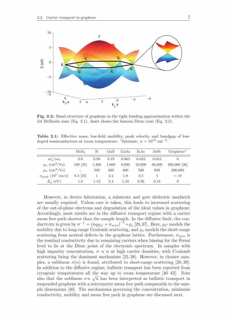
of electron and hole symmetry, the plus and minus signs correspond to theconduction (π∗) and valence (π) bands, respectively. The NNTB model agreeswell with ab initio calculations within ± 1 eV of the intrinsic Fermi energylevel, EF = 0 eV, where the conduction and valence bands touch without abandgap. The bandstructure of graphene is illustrated in Fig. 2.2.
The performance of graphene-based electronic devices is governed mainlyby the dispersion when |E| < 0.4 eV, the EF range reachable by field- orimpurity-induced carriers. This corresponds to the regions closest to the six Kand K′ points of the first Brillouin zone. Here, the energy-momentum relationis further simplified to a cone - see the inset of Fig. 2.2 - given by
E(k) = ±�vF
√k2x + k2y. (2.2)
In Eq. 2.2, � is Planck’s constant, and vF= 3γa/2� � 108 cm/s is the Fermivelocity (upper limit of the carrier velocity) in graphene within the tight bind-ing approximation. The linear dispersion indicates massless particles describedby the Dirac equation, giving the names Dirac points where the conduction andvalence bands meet. These massless particles, the so-called Dirac fermions,represent the origin of the superior carrier mobilities expected in graphene.
2.2 Carrier transport in graphene
The high-frequency performance of FETs depends on the carrier dynamics inthe channel, quantified by the mobility and peak velocity, i.e., the responseof the carriers to an applied electric field. Graphene is compared with Si,III-V semiconductors and single-layer MoS2 in Table 2.1. The intrinsic cut-off frequency, i.e., the high-frequency limit of a material, can be related tothese properties. In principle, fT,int =
v2πLg
, where the carrier velocity in the
channel is ultimately bound by the peak velocity v = vpeak. In practice, theimportance of the peak velocity increases compared to the mobility due tohigher electric fields when scaling the gate length. Clearly, graphene appearsto be an outstanding candidate to reach extremely high frequencies.
2.2. Carrier transport in graphene 7
−4−2024
−50
5
−10
−5
0
5
10
kx a
k y a
E (e
V)Γ
Κ
Κ’Κ’
Κ’ Κ
Κ
Fig. 2.2: Band structure of graphene in the tight binding approximation within the1st Brillouin zone (Eq. 2.1). Inset shows the famous Dirac cone (Eq. 2.2).
Table 2.1: Effective mass, low-field mobility, peak velocity and bandgap of low-doped semiconductors at room temperature. ∗Intrinsic, n ∼ 1012 cm−2.
MoS2 Si GaN GaAs InAs InSb Graphene∗
m∗e/m0 0.6 0.98 0.19 0.063 0.023 0.015 0
μe (cm2/Vs) 100 [35] 1,400 1,600 8,000 33,000 88,000 200,000 [36]
μh (cm2/Vs) - 500 200 400 500 850 200,000
vpeak (107 cm/s) 0.3 [35] 1 2.4 1.8 3.5 5 ∼ 10
Eg (eV) 1.8 1.12 3.4 1.43 0.36 0.18 0
However, in device fabrication, a substrate and gate dielectric sandwichare usually required. Unless care is taken, this leads to increased scatteringof the out-of-plane electrons and degradation of the ideal values in graphene.Accordingly, most results are in the diffusive transport regime with a carriermean free path shorter than the sample length. In the diffusive limit, the con-ductivity is given by σ−1 = (nqμC + σmin)
−1+ρs [28,37]. Here, μC models the
mobility due to long-range Coulomb scattering, and ρs models the short-rangescattering from neutral defects in the graphene lattice. Furthermore, σmin isthe residual conductivity due to remaining carriers when biasing for the Fermilevel to lie at the Dirac point of the electronic spectrum. In samples withhigh impurity concentration, σ ∝ n at high carrier densities, with Coulombscattering being the dominant mechanism [22, 38]. However, in cleaner sam-ples, a sublinear σ(n) is found, attributed to short-range scattering [28, 39].In addition to the diffusive regime, ballistic transport has been reported fromcryogenic temperatures all the way up to room temperature [40–42]. Notealso that the sublinear σ∝ √
n has been interpreted as ballistic transport insuspended graphene with a micrometre mean free path comparable to the sam-ple dimensions [40]. The mechanisms governing the concentration, minimumconductivity, mobility and mean free path in graphene are discussed next.

8 Chapter 2. Graphene properties for high-speed electronics
−0.3 −0.2 −0.1 0 0.1 0.2 0.310
4
106
108
1010
1012
1014
EF (eV)
n, p
(cm
−2)
n-type
p-type
Closed form
−0.3 −0.2 −0.1 0 0.1 0.2 0.30
1
2
3
4
5
6
7
8
E (eV)
DO
S (
10
13 e
V−1cm
−2)
Graphene
GaAs 2DEG
a) b)
Holes Electrons
Fig. 2.3: a) Carrier concentrations versus EF at room temperature [23] and b) DOSin graphene compared with an AlGaAs/GaAs 2DEG with ns = 0.67 ·1012 cm−2 [44].
2.2.1 Gate-induced versus residual carrier concentration
Due to the gapless spectrum of graphene, either electron or hole carriers maybe induced by shifting the Fermi level. This can be accomplished via the fieldeffect [22], charge transfer from metal contacts to graphene [43] or moleculesadsorbed on the graphene surface [26]. The carrier concentration versus theFermi level and the density of states (DOS) versus energy level in graphene atroom temperature are plotted in Fig. 2.3. The carrier density can easily exceedthat of a two-dimensional electron gas (2DEG) where ns ∼ 1012 cm−2 [44]. Infact, with the Al2O3 dielectric in the devices fabricated as part of this thesis,n > 1 · 1013 cm−2 is easily attained at a top-gate voltage Vg � 5 V.
Importantly, without external bias and at room temperature, the thermalcarrier concentration in the absence of a bandgap is given by
nth =π
6
(kBT
�vF
)2
, (2.3)
which results in nth = 8·1010 cm−2. The concentration of carriers is identicallyzero only at T = 0 K, for ideal and perfectly clean graphene. All experimentalgraphene, however, requires an additional parameter to explain the behaviourat the minimum conductivity point, i.e., the gate voltage that most closelycorresponds to the Dirac point of the electronic spectrum. This parameter isthe so-called residual carrier density, n0. In particular, σmin exhibits a widerplateau at room temperature [38] and a weaker temperature dependence uponcooling than expected solely from thermal generation [40]. It is the resultof a spatially inhomogeneous potential created by impurities in the substrateor at the graphene-substrate interface, with concentration nimp [39]. As aconsequence, the degree of disorder and thus the residual carrier concentrationare highly substrate-dependent properties. It ranges from 1011 − 1012 cm−2
on SiO2/Si samples [38] via ∼ 1010 cm−2 on h-BN [28] to ∼ 108 cm−2 in acurrent-annealed, suspended sample [37]. As a rule of thumb, the temperaturedependence of σmin is suppressed unless kBT > Epuddle = �vF
√πn0.

2.2. Carrier transport in graphene 9
2.2.2 Extraction of the low-field mobility
At low transverse electric fields, the carrier drift velocity is linear in fieldstrength with the low-field mobility, vdrift =μE . The carrier mobility is thusa decisive property for the FET speed at long gate lengths. Several distinctways to extract the carrier mobility exist, and some care should be taken incomparing the values obtained by the different methods [45].
First, the Hall effect mobility in graphene can be measured on a dedicatedHall bar [22,40] or van der Pauw [46,47] structure with the aid of a transversemagnetic field. Because the mobility and the carrier concentration appear asa product in the expression for resistivity, a Hall measurement is the onlymethod that unambiguously separates them.
Second, the conductivity mobility defined explicitly by μ ≡ σnq is sometimes
reported for graphene [22, 41, 48]. The conductivity, σ, is derived from thefour-contact resistance of a graphene patch with well-defined dimensions. Thecarrier density, n, is estimated via the gate capacitance and voltage.
Third, the field-effect mobility defined by the slope of the conductivitycurve μ ≡ 1
Cg
dσdVg
is occasionally presented [28, 49]. Likely the most common
method for graphene is a variant of the field-effect mobility based on fitting ofthe GFET transfer characteristics [50]. This is valid for samples with mobilitylimited by charged impurity scattering, where σ ∝ n, which yields one carrier-density-independent value for conductivity mobility. The contact resistance isexcluded by fitting to the complete expression
Rtot = 2Rc +Rchannel = RS +RD +Lg
Wgqμ
√n20 +
(Cg(Vg−VDirac)
q
)2, (2.4)
where 2Rc is the sum of the drain and source contact resistances. This is themethod of choice to extract mobility for the GFETs reported in this thesisbecause no special test structure is required to be fabricated.
2.2.3 Limitations on the low-field mobility in graphene
The dielectric environment in most cases limits transport in graphene to thediffusive regime. Several carrier scattering mechanisms recognised to limit themobility of graphene are listed below. The list starts from the fundamentalmechanisms and moves on to the detrimental limitations of the common SiO2
substrates, and the discussion finally moves on to its possible replacement.
• Longitudinal acoustic phonons (LAP) [36]: The theoretical upperbound for mobility is set by the LAP interaction. It contributes with theresistivity of 30 Ω/sq at room temperature independent of concentration[36]. Although this results in a mobility μ ∼ 200, 000 cm2/Vs at a carrierconcentration n = 1012 cm−2, it drops rapidly as μ ∝ 1/n.
• Charged impurities (Coulomb scattering) [38, 39]: For grapheneon SiO2, the phonon scattering is masked by typical impurity densitieswhich limit the experimental mobility to ∼ 10, 000 cm2/Vs [22,50].

10 Chapter 2. Graphene properties for high-speed electronics
Table 2.2: Temperature dependence of resistivity, ρ, as a result of scattering mech-anisms in graphene. E0 is the energy of the surface optical phonon mode.
Scattering mechanism T interval T dependence
Longitudinal acoustic phonons [36] T > 20 K ρ ∝ T
Charged impurities (Coulomb) [36] ∀ T None
Remote interfacial phonons [36] ∀ T ρ ∝ 1eE0/kBT−1
Flexural phonons [52] ∀ T ρ ∝ T 2
• Remote interfacial phonons (RIP) [36,51]: Even in the ideal case ofno charged impurities, the lowest RIP mode of SiO2 (59 meV) would setan upper limit of 40,000 cm2/Vs at room temperature [36]. Exchangingthe SiO2 substrate for a high-ε substrate screens the impurities but atthe expense of low-energy surface optical phonons. This increases RIPscattering and results in a small improvement at 300 K [51].
• Flexural phonons (FP) [52]: This represents a dominant mechanismof scattering in free-standing graphene samples. It consists of staticripples introduced on rough substrate surfaces that are frozen in whensuspending the graphene.
Along these lines, h-BN provides an alternative substrate with a numberof valuable properties [28]. It has the same hexagonal structure as graphenewith a lattice mismatch of only ∼ 2%. The surface of h-BN is inert, drasticallyreducing the attachment of impurities compared with SiO2. As a result, onebenefits from the higher RIP modes of h-BN (>100 meV) while maintainingthe gating ability of SiO2 (εh−BN ∼ εSiO2) and without losing performancedue to the weak impurity screening. At room temperature, graphene on h-BN [42] may show significantly higher mobility than suspended graphene [52].Graphene conforms to the extremely smooth surface of h-BN, therefore limit-ing the scattering on graphene ripples. In fact, mobilities at the LAP limit atroom temperature have been shown for graphene encapsulated in h-BN [41].In addition, h-BN would allow for benefits in cooled graphene devices, as con-cluded from Table 2.2. At carrier concentrations n � nth, the mobility has aninverse temperature dependence compared with the resistivity. The large-scalefeasibility of graphene and h-BN synthesis is discussed in Section 2.3.
2.2.4 High-field carrier velocities in graphene
In general, in high electric fields, the carrier velocity reaches a peak value beforeapproaching the saturated velocity. However, in graphene, a soft saturationwithout peak is observed, which is described by [48]
vdrift =μE(
1 + (μE/vsat)γ)1/γ , (2.5)
where μ is the low-field mobility, and vsat is the saturated carrier velocity. Atshort gate lengths, the saturation velocity is thus a more crucial parameter for

2.2. Carrier transport in graphene 11
graphene than the mobility to make a fast FET. The saturation velocity ingraphene is bound by the optical phonon energy, the carrier concentration andthe temperature as a result of phonon occupation, NOP = 1/(e�ωOP /kBT − 1).This can be well predicted by the simple model
vsat =2ωOP
π√πn
√1− ω2
OP
4πnv2F
1
NOP + 1. (2.6)
For ideal graphene, the saturation velocity is theoretically bound by the Fermivelocity, vF = 108 cm/s, by the intrinsic phonon mode, �ωOP = 160 meV,in the limit of low carrier concentration. On SiO2, however, it is severelydeteriorated as a result of the substrate surface optical phonon mode withlower energy, �ωOP = 55 meV [48]. Consequently, the extracted vsat on SiO2
and SiC is in the range of 1−2 ·107 cm/s. Higher drift velocities by a factor oftwo should be possible if the substrate limitation can be overcome. In addition,for nanometre sized GFETs, the high-frequency limit can be enhanced bytransient velocity overshoot [53], observed also in III-V semiconductors [44].
2.2.5 Opening a bandgap in graphene
In GFETs, a bandgap in graphene is desirable for improved performance ofthe devices. Two main routes are to induce it either by lateral confinement ina graphene nanoribbon or by a perpendicular field in bilayer graphene.
First, in graphene nanoribbons, the bandgap depends inversely on thewidth, w, as Eg = α/w. The proportionality constant crucially depends onthe edge structure and roughness [54]. Ribbons prepared by electron beamlithography and oxygen plasma etching have well-defined orientation in ar-rays. However, the edge roughness sets limits on α = 0.2 eV·nm and thewidth is restricted to w > 10 nm [55]. Moreover, ribbons thermally exfoliatedfrom graphite and sonicated enabled w ∼ 2 nm [56]. In addition, these rib-bons had significantly smoother edges. Consequently, for α = 0.8 eV·nm, alarge Eg ∼ 0.4 eV and an ION/IOFF ratio ∼ 106 at room temperature weredemonstrated. The disadvantages include random positions, directions and nocontrol of ribbon sizes. Similarly, isolated sub-nanometre ribbons with per-fect edges have been fabricated by self-assembly [57]. However, without thepossibility for array fabrication, they are useless for microwave transistors.
Second, breaking bilayer graphene symmetry opens a bandgap [58]. Dif-ferent amounts of carriers are introduced in the two layers from the top andbottom sides of the bilayer. Preferably for applications, double-gated FETshave been used to introduce a tuneable bandgap [59]. A gap up to 0.25 eV [58]and an on-off ratio ∼ 100 at room temperature [59] was achieved using com-bined top and backgates. Another option is the use of substrates with built-infields, such as SiC [60] or ferroelectric LiNbO3 [Paper H].
However, the mobility in graphene severely degrades as a sizeable bandgapis opened, following the same trend as for conventional semiconductors [17].The highest mobilities reported at room temperature for 20 nm and 50 nm widegraphene nanoribbons are 2,000 cm2/Vs and 3,000 cm2/Vs, suspended [61]and on substrate [62], respectively. In the same way for bilayer graphene,the intrinsic mobility is severely degraded by the re-shaped bandstructure to∼ 10, 000 cm2/Vs at a sizeable bandgap necessary for applications [63].

12 Chapter 2. Graphene properties for high-speed electronics
12 μm
40 μm
20 μm
a) b)
1400 1800 2200 2600 30000
0.5
1
−1
Inte
nsi
ty (
a.u
.)
Raman shift (cm )
G
2D
1400 1800 2200 2600 30000
0.5
1
Raman shift (cm )-1
Inte
nsi
ty (
a.u
.)
G
2D
D
Fig. 2.4: Optical identification of single-layer graphene on SiO2/Si substrate by a)exfoliation and b) CVD growth on Cu catalyst in a virtually hole-free area. Theinsets show the respective Raman signature characteristic of monolayer graphene.
2.3 Practical status of graphene synthesis
The term graphene has different meanings depending on the intended appli-cation, e.g., in terms of number of layers, electronic quality or visual trans-parency. This subsection describes the graphene synthesis methods relevantwithin the scope of this thesis. It concludes with the motivation and implica-tions of the graphene used for the device and circuit demonstrators herein.
2.3.1 Exfoliation from highly ordered graphite
Mechanical exfoliation provides graphene of highest quality for fundamentalresearch, whereas liquid phase exfoliation provides inexpensive graphene inlarge quantities for low-cost and low-performance applications.
The Scotch tape method, i.e., peeling off single layers from bulk graphite,was first demonstrated systematically in 2004 [22]. It still produces the highestmobility and lowest defect density graphene. The best mobilities both insuspended samples at T = 240 K of ∼100,000 cm2/Vs [40] and at 5 K of1,000,000 cm2/Vs [52] as well as on substrate (hexagonal boron nitride) atT = 230 K of ∼100,000 cm2/Vs [49] and at 4 K of ∼140,000 cm2/Vs [49] usemechanically exfoliated material at a carrier density of 1011 cm−2. Translatedto a mean free path, this means micrometre-scale ballistic transport. TheGFETs in [Paper D] and [Paper E] are fabricated on exfoliated graphene. Aflake made by mechanical exfoliation of is shown in Fig. 2.4a).
On the other end of the scale, mass exfoliation from graphite flakes in liq-uids by sonication or shear-mixing produces few-layer graphene flakes suitablefor inkjet printing [64]. The resulting graphene is multi-flake but could reachacceptable sheet resistance for certain applications and mobility comparableto metal oxide semiconductors such as IGZO for flexible active devices.
2.3.2 Graphene and h-BN synthesis by CVD
The possibility of growing thin graphitic films by CVD on different metalsurfaces has been long explored. The development led to the currently most

2.3. Practical status of graphene synthesis 13
promising technique for the CVD growth of single-layer graphene, which is onCu foils [29]. Graphene is formed on Cu mainly by the surface-catalysed de-composition of a methane precursor, given the extremely low carbon solubilityin Cu [65]. Once a layer of graphene covers the surface, the catalytic effectceases, which results in a growth closely self-limited to a single layer. Indeed,up to 95% of the grown material can be controlled to be monolayer.
In this thesis, graphene was grown on 50 μm thick and 99.995+ % purityCu foil in a cold-wall CVD system (Black Magic, AIXTRON), based on therecipe by Sun et al. [66]. The foils are pre-cleaned in acetone, isopropanol andacetic acid to remove organic contaminants and native oxides. The copper isannealed in situ for 5 min in 20 sccm H2 and 1,000 sccm Ar ∼ 1, 000 ◦C. Inaddition to having a reductive effect on remaining oxygen, this increases thegrain size of the Cu, thus improving the domain size of the grown graphene.Finally, the carbon precursor gas, 30 sccm methane (CH4) diluted to 5% in Ar,is introduced. After 5-10 min, while maintaining a temperature ∼ 1, 000 ◦C,the methane gas is turned off and the catalyst is cooled to room temperature.
The major drawbacks of the in-house CVD growth reactor are the poortemperature control and uniformity over the copper surface [67]. Uncontrolledgrowth temperature and excess particle contamination in the system lead tovariations of the graphene nucleation density. The resulting films consist ofmany small, coalesced graphene domains (� 5 μm) with different orientations(Fig. 2.5). Between the domains, the grain boundaries act as line defects thatincrease the carrier scattering and deteriorate the graphene mobility. Never-theless, the Raman spectra of the in-house CVD graphene in a low-doped area[Paper H] is comparable to the exfoliated samples. Consequently, the CVDgraphene exhibits I2D/IG ∼ 2, an FWHM of the 2D peak ∼ 35 cm−1 and onlya small D peak ID/IG ∼ 0.2, as shown in Fig. 2.4b).
Recently, tremendous efforts have been undertaken by many research groupsto reduce the nucleation density and grow large single-domain graphene crys-tals. These include optimisation of the methane partial pressure [68], pre-growth polishing of the Cu foil to remove defects and grain boundaries whichact as nucleation centres [69], non-reducing pre-annealing conditions to reducethe graphene nucleation by remaining copper oxide [70] and even intentionalpassivation with oxygen [71]. Altogether, centimetre-scale isolated and ran-domly positioned grains have been achieved with an order of magnitude bettermobility. The growth time, however, is inherently longer due to the low car-bon source supply and can be up to several days. Notably, for continuous filmssuitable for device applications, the largest grain size reported is ∼ 1 mm [46].
Graphene and atomically flat hexagonal boron nitride should be consideredas a system and preferably be synthesised in situ by CVD at the wafer scale.Recently, it has been shown that single-domain CVD graphene on exfoliated h-BN can reach mobilities on the same order as exfoliated samples [42]. However,the CVD growth of h-BN on metal catalysts or catalyst-free graphene growthdirectly on h-BN is much less mature, with limited domain size and poor layercontrol [72]. Different experimental conditions have been explored, includingwet layer-by-layer transfer of CVD graphene from Cu foil onto CVD h-BNfrom Fe foil [73], CVD growth of nanometre graphene flakes onto exfoliatedh-BN [74] and sequential growth of CVD graphene onto CVD h-BN on Cu [75].None of the above are repeatable processes at the wafer scale.
14 Chapter 2. Graphene properties for high-speed electronics
10μm
a) b)
10μm
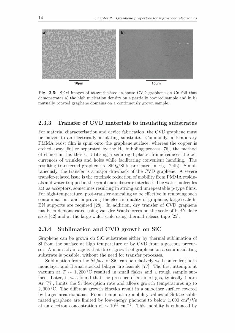
Fig. 2.5: SEM images of as-synthesised in-house CVD graphene on Cu foil thatdemonstrates a) the high nucleation density on a partially covered sample and in b)mutually rotated graphene domains on a continuously grown sample.
2.3.3 Transfer of CVD materials to insulating substrates
For material characterisation and device fabrication, the CVD graphene mustbe moved to an electrically insulating substrate. Commonly, a temporaryPMMA resist film is spun onto the graphene surface, whereas the copper isetched away [66] or separated by the H2 bubbling process [76], the methodof choice in this thesis. Utilising a semi-rigid plastic frame reduces the oc-currences of wrinkles and holes while facilitating convenient handling. Theresulting transferred graphene to SiO2/Si is presented in Fig. 2.4b). Simul-taneously, the transfer is a major drawback of the CVD graphene. A severetransfer-related issue is the extrinsic reduction of mobility from PMMA residu-als and water trapped at the graphene substrate interface. The water moleculesact as acceptors, sometimes resulting in strong and unrepeatable p-type films.For high-temperature, post-transfer annealing to be effective in removing suchcontaminations and improving the electric quality of graphene, large-scale h-BN supports are required [28]. In addition, dry transfer of CVD graphenehas been demonstrated using van der Waals forces on the scale of h-BN flakesizes [42] and at the large wafer scale using thermal release tape [25].
2.3.4 Sublimation and CVD growth on SiC
Graphene can be grown on SiC substrates either by thermal sublimation ofSi from the surface at high temperature or by CVD from a gaseous precur-sor. A main advantage is that direct growth of graphene on a semi-insulatingsubstrate is possible, without the need for transfer processes.
Sublimation from the Si-face of SiC can be relatively well controlled; bothmonolayer and Bernal stacked bilayer are feasible [77]. The first attempts atvacuum at T ∼ 1, 200 ◦C resulted in small flakes and a rough sample sur-face. Later, it was found that the presence of an inert gas, typically 1 atmAr [77], limits the Si desorption rate and allows growth temperatures up to2, 000 ◦C. The different growth kinetics result in a smoother surface coveredby larger area domains. Room temperature mobility values of Si-face subli-mated graphene are limited by low-energy phonons to below 1, 000 cm2/Vsat an electron concentration of ∼ 1013 cm−2. This mobility is enhanced by

2.3. Practical status of graphene synthesis 15
hydrogen intercalation, effectively decoupling the graphene from the substrateto make it quasi-free-standing, to 3, 000 cm2/Vs [78].
Recently, the CVD growth on the Si-face of SiC including in situ hydrogenintercalation was reported for synthesis of both monolayer [47] and bilayer [60]graphene. The obtained hole concentration was shown to closely match thatinduced by the spontaneous polarisation of the SiC substrate, indicating thehigh quality of the films. Accordingly, the mobilities reach 6,000 cm2/Vs asmeasured over 10×10 mm2 areas. Due to the pre-growth surface annealingstep used in both the sublimation and CVD methods, step bunching on theSiC surface occurs. Terraces of 5-10 μm width form where the grown grapheneis mono- or bilayer, depending on the recipe, whereas on the 5-10 nm stepsseparating the terraces, an additional layer forms. Smaller terrace widthsand step heights and higher mobilities occur closer to the SiC wafer centre,indicating the importance of a high-quality starting material [47].
Controlling the sublimation rate of silicon from the C-face of SiC is morechallenging, and stacks of mutually rotated, decoupled monolayers are formed.Nevertheless, the C-face epitaxial graphene displays up to several times highermobility than the Si-face [79], as a result of a different interface structure,proving its potential for high-frequency electronics.
2.3.5 Which type of graphene and why?
Considering applications of graphene, the described large-volume productionmethods can be divided as suitable either for high-performance electronicsin which a higher cost is acceptable or for mass deployment in medium-performance applications where a lower cost is necessary. In both cases, bilayergraphene is desirable for electronics because it allows a bandgap to be opened.
The graphene on SiC belongs to the first category. Directly synthesisedon a semi-insulating substrate, it is mainly well suited for RF electronics andresistance standards [80]. Moreover, the growth of bilayer graphene is wellcontrolled, and a bandgap may be induced in this material for free due to thespontaneous polarisation of the SiC substrate.
The CVD graphene has prospects mostly for the second category. Thetransfer of CVD graphene is both a major advantage in terms of versatility, inthat it can be transferred from the catalyst to any host substrate in principle,and a quality and reproducibility issue at the same time. The transfer allowsfor applications in transparent conductors [25] and as a ubiquitous platformfor flexible active devices on plastics [27]. In addition, CVD graphene canpotentially be integrated into standard CMOS processes, in the back-end-of-line after careful consideration of the temperature budget and metal cross-contamination from etched Cu foil residuals [30]. However, the growth ofcontinuous AB-stacked bilayer graphene by CVD is not yet achieved. Someefforts utilise the catalytic effect of Cu in a region spatially separated from thegrowth region [70]. Bilayer crystals with mobility of ∼20,000 cm2/Vs and abandgap opened by a vertical field have been grown on the outside of a Cu foilenclosure, using carbon diffused from the catalytically active inner surface [81].
Printed graphene from flakes exfoliated in liquid may complement CVDgraphene in interconnects and transparent conductors where a higher sheetresistance is acceptable to make a universal electronics platform.

16 Chapter 2. Graphene properties for high-speed electronics
In summary, the applicability of CVD graphene to different substrates bestenables the exploitation of the unique properties of graphene as a material forthe opening of new niche applications. Furthermore, to conform with utility inapplications, continuous CVD graphene is used throughout this thesis, despiteits lower mobility < 2, 000 cm2/Vs [66]. A condensed summary of the synthesismethods discussed is given in Table 2.3. For graphene to ever compete withIII-V high-speed devices, a major breakthrough in the synthesis of h-BN andlarge-domain bilayer graphene heterostructures at the wafer scale is necessary.
Table 2.3: Comparative summary of graphene growth methods and associatedproperties relevant to applications. The mobility values are for supported grapheneon the following substrates and at room temperature: 1) SiO2/Si and
2) h-BN. Forthe CVD growth on Cu foil, † isolated single crystals and ‡ coalesced continuous film.
Scalability
limit
Layer
control
Domain
size
Mobility(cm2/Vs
) Cost Versatility
Mechanical
exfoliation [49]
Graphite
grainsPoor < 1 mm
20,0001)-
100,0002)High Research
CVD† on
Cu-foil [71]
Domain
size
Good
(≤ 1L)< 50 mm
10,0001)-
30,0002)High Medium
CVD‡ on
Cu-foil [46]
Reactor
dimensions
Good
(≤ 1L)< 1 mm < 6,0001) Medium High
Sublimation
Si-face [78]
SiC wafers
< 6 inch
Good
(≤ 2L)< 10 μm < 3,000 High Low
CVD on
SI SiC [47]
SiC wafers
< 6 inch
Good
(≤ 2L)< 10 μm < 6,000 High Low
Sublimation
C-face [79]
SiC wafers
< 6 inchPoor - < 30,000 High Low
Liquid
exfoliation [64]
Ink-jet
printerPoor < 1 μm < 100 Low Medium

Chapter 3
Fabrication, device-levelcharacterisation andmodelling of GFETs
This chapter discusses the operation principles, performance indicators andmodelling of GFETs in active amplifiers and passive detectors and mixers. Todesign GFET-based circuits, characterisation and model development at thedevice level are necessary. This thesis contributes a small-signal analysis ofpassive GFET power detectors in [Paper A]. The large-signal model proposedin [82] is used to design and analyse resistive GFET mixers in [Paper C] and[Paper D]. In addition, active GFETs used for amplification are distinguishedby their small-signal gain and noise figure, which are the topics of [Paper F].
3.1 Device fabrication
The measurement frequency and characterisation environment dictate whetherthe device is laid out with coplanar pads for on-wafer access or an antennafor free-space characterisation. However, the fabrication flow is analogous inboth cases. Subsequent to graphene growth and transfer, an electron beamlithography-based process is used to fabricate test structures and GFETs. Thegeneral steps are illustrated in Fig. 3.1 and motivated by references below. Alldetailed process parameters are listed in Appendix A.
• Mesa- and nanoconstriction etching in O2 plasma at 50 W RFpower and 50 mTorr pressure for 6 s using a negative resist mask. Thisstep provides device isolation and improves the current on-off ratio [83].
• Ohmic contacts (1 nm Ti/15 nm Pd/100 nm Au) are formedby evaporation and lift-off. The thin Ti is used as an adhesion layer,whereas low contact resistance is assured by the Pd layer [84, 85].
• Annealing in Ar ambient at 230 ◦C for 15 min which helps to re-move residual PMMA in the channel region [86] and reduces the contactresistance for chemisorbed metals on graphene such as Pd [87].
17

18 Chapter 3. Fabrication, device-level characterisation and modelling of GFETs
• Atomic layer deposition (ALD) at 300 ◦C for 15 nm Al2O3 oftop-gate oxide. Prior to the ALD deposition, a seed layer of 4× 1.5 nmin thickness is formed by natural oxidation of evaporated Al [50].
• Gate fingers with 100 nm access gaps are patterned and metallisedwith 10 nm Ti/300 nm Au or 250 nm Al/10 nm Ti/50 nm Au.
• Coplanar pads or antennas (10 nm Ti/300 nm Au) overlappingthe ohmic metal are formed on the SiO2 surface by evaporation. First,the Al2O3 is etched in buffered oxide etch, with the Au as the etch stop.Coplanar access and antenna-coupled GFETs are shown in Fig. 3.2.
Graphene Al2O3Ohmic
Si
SiO2
Si
SiO2
DS S
Si
SiO2
DS S
Si
SiO2
DS S
Si
SiO2
DS SGG
Si
SiO2
DS SGG
Gate Pad
GG
Fig. 3.1: Schematics of the fabrication steps for a two-finger GFET.
3.2 DC characterisation of GFETs
To realise high-performance FETs, it is important to fabricate high-qualityohmic contacts and graphene with low sheet resistance. Extraction of mobilityand contact resistance from DC measurements is thus important for bothyield analysis and models to predict the RF performance of the devices. Mostimportantly, these parameters reflect directly on the transconductance.

3.2. DC characterisation of GFETs 19
a) b)
Gate
Source
Drain
Source Drain
Gate
Gate
Source
20 μm20 μm
Fig. 3.2: Two finalised GFETs outlined with a) coplanar access pads for on-wafercharacterisation and b) a broadband bow-tie antenna for free-space characterisation.
3.2.1 Ohmic contacts to graphene
The parasitic source and drain resistances in a symmetric FET layout areequal and may be expressed as a sum of the interface resistance and the accessresistance, RS = RD = (RcW+RshLa)/Wg, where RcW is the metal-graphenecontact resistance, Rsh is the sheet resistance, La is the access gap length, andWg is the gate width. Achieving a good ohmic contact to graphene has been thesubject of extensive study, and the mechanisms have been gradually clarified.
• Early work focused on the “side-contact” geometry, i.e., a picture inwhich the deposited metal is thought to lie on the graphene surface. Thelow contact resistivity with high work function metals such as Pd [84] andNi [88] was attributed to charge transfer and resulting DOS enhancement[43]. For this type of contact, a clean interface is required [89]. This wasachieved in this work using an e-beam resist process.
• On this line, a high starting carrier concentration in the graphene is mosteffective, which was proved by gating to be independent of the carrier sign[84]. This is an inherent property in epitaxially grown graphene, wherelow contact resistances have been repeatedly reported [90]. However,selective doping of graphene is desired to produce a device structuresimilar to the use of cap layers in HEMTs [44].
• Recent studies elucidated the advantage of using a chemisorbed metalcontact on graphene in an “edge-contact” geometry [41]. Metals such asNi, Pd and Ti chemisorb on graphene [43] and bind particularly stronglyto reactive sites such as graphene edges. The edges can be formed ingraphene defected by O2-plasma ashing [91] or metal-catalysed etch-ing [88] or in a controlled manner by lithographic patterning [92,93]. Infact, spontaneous end-contact formation after deposition of chemisorbedmetals on CVD graphene was reported [85], which could be further en-hanced after annealing [87].
In this work, a large variability of contact resistances within batches hasbeen observed. A large dataset of two-probe contact resistances to CVDgraphene is summarised in Fig. 3.3, yielding a mean RcW ∼ 600 Ωμm.

20 Chapter 3. Fabrication, device-level characterisation and modelling of GFETs
Fig. 3.3: Two-probe contact resistance extracted with Eq. 2.4. The distribution isfor ∼100 GFETs from batches fabricated in the process of [Paper A] and [Paper C].
0 200 400 600 8000
5
10
15
20
25
30
35
Contact spacing (nm)
Rto
t (Ω)
SiO2
/Si
2Rc
Au Au
Graphene
W=30μm
L
Rsh ~600 Ω/sq
−5 0 5 10 15 20 25 300
20
40
60
80
100
120
140
160
180
Rto
t(Ω
)
SiO2/Si
Gap spacing (μm)
Fused Silica
a bs
Au
Au
Graphene
2Rc
Rsh ~1300 Ω/sq
a) b)
Fig. 3.4: TLM results for CVD graphene on SiO2/Si substrates with a) Pd basedcontact which gives RcW = 80 Ωμm [Paper F] and b) Ti metallised contact withRcW = 900 Ωμm [Paper G]. The insets illustrate the TLM structure layouts.
Better accuracy is obtained within the four-probe transmission line method(TLM) measurements. Using this extrapolation approach, which is illustratedin Fig. 3.4, resistivities for the contacts reach the state of the art; <100 Ωμmwith Pd metallisation [Paper F] and 900 Ωμm with Ti metallisation [Paper G]were reported, respectively. As discussed above, a combination of high carrierconcentration and edge-contact formation is the likely explanation for the lowvalue in [Paper F]. An accurate determination of a small RcW with a large Rsh
and an inhomogeneous material becomes a delicate task [89]. Consequently,the TLM layout was designed as shown in the inset of Fig. 3.4a) to have smallresistance, Rtot = 2Rc + RshL/W . In addition, the narrow contact spacingswere measured with SEM.

3.2. DC characterisation of GFETs 21
0 2 4 6 8 10
n0
(10 12 cm -2)
10
100
1000
Mob
ility
(cm
2/V
s)
Paper A - SiO 2
Paper B - SiO 2
Paper C - SiO 2
Paper F - SiO 2
Paper H - SiO2
Paper H - LiNbO 3
Fig. 3.5: Compilation of hole mobilities versus the residual concentrations extractedfrom fitting of Eq. 2.4 using top gates. All devices were fabricated on CVD graphenein different batches during the work on the papers appended to this thesis.
3.2.2 Channel mobility and sheet resistance
The mobility values reproduced in Table 2.3 are measured for graphene on asubstrate. However, in current GFET structures with top gates, the grapheneis usually sandwiched between two oxide interfaces, as shown in Fig. 3.1. Theseeded ALD deposition of Al2O3 used herein has been shown to preserve themobility well in exfoliated graphene [50]. Extending the results in [Paper H],a larger collection of mobilities and residual carrier concentrations extractedfrom least squares fitting to Eq. 2.4 are shown in Fig. 3.5. According to [38],all of these CVD samples are considered to be “dirty” (with high impurityconcentration nimp), compared with the exfoliated samples in [Paper D] and[Paper E] with n0 ∼ 5 · 1011 cm−2, which are relatively “clean”. Building onthe analysis in [Paper H], one reason for the variation is an irregular Al2O3
dielectric quality, most likely exacerbated by the requirement for a seed layer.
In addition to active devices calling for high mobilities, passive componentsas transparent electrodes [25] and antennas [Paper I] are also considered. Theserequire only to minimise the graphene sheet resistance, Rsh= (qnμ)−1. Thecombination of low sheet resistance and high transparency together with thevariety of envisioned substrates necessitates CVD graphene. Typical valuesfor sheet resistance in this work are 0.5 - 1 kΩ/sq, from the TLM graphsin Fig. 3.4. Attempts to further reduce the sheet resistance used surface-functionalised multilayer CVD graphene. However, the reproducibility andstability of chemical treatments are questionable. The most promising routeis the FeCl3 intercalation process. The competitiveness of graphene to ITO issummarised in Table 3.1. Typical application requirements are 10-100 Ω/sqfor transparent electrodes [25]. This means that graphene is practically viablefor transparent conductors in touchscreens, where it can replace the expensive,rare and brittle indium tin oxide (ITO) currently used. Graphene for antennasis further discussed in Section 4.6.

22 Chapter 3. Fabrication, device-level characterisation and modelling of GFETs
Table 3.1: Rsh and T for graphene versus # layers and chemical treatment.a Layer-by-layer transfer, Cu catalyst. b Intercalated, Cu-Ni catalyst.
# layers Treatment Rsh (Ω/sq) T (%) Removal Ref.
1 - 4a PMMA 130 - 40 97 - 90 - [25]
1 - 4a HNO3 110 - 30 97 - 90 Desorbs in air [25]
1 - 4a FeCl3 95 - 55 - H2O adsorption [94]
2 - 4b FeCl3 400 - 20 95 - 90 Stable in air [95]
ITO - 100/10/2 90/85/80 - -
0 50 100 150 200 250
Gate width (μm)
100
1000
gm
, gd
s (mS/
mm
)
gm
- [Zhang 2016]
gds
- [Zhang 2016]
gm
- [Paper E]
gds
- [Paper E]
gm
- [Paper F]
gds
- [Paper F]
SiC GFETs - gm
SiC GFETs - gds
CVD GFET - gm
CVD GFET - gds
Fig. 3.6: Extrinsic transconductance and output conductance of the CVD GFETsin [96], [Paper F] and the exfoliated GFET [Paper E]. For comparison, the reportedvalues for ultrathin gate oxide SiC [21,97,98] and CVD [99] GFETs are given.
3.2.3 Transconductance and output conductance
The extrinsic transconductance, gme = dIds/dVgs, and output conductance,gde = dIds/dVds, provide a connection between the DC and RF performanceof an FET through the low frequency small-signal gain
|S21| = 2Z0gme
1 + Z0gde. (3.1)
An overview of the devices used in the fabricated amplifiers in this thesis isgiven in Fig. 3.6. Scaling the gate width, higher gain can be achieved bythe increased gme, but the effect is diminished by the simultaneous increaseof gde. Extreme scaling of the gate oxide thickness at gate lengths ≤ 250 nm,good mobility in SiC graphene and low contact resistances are responsible forthe impressive transconductances in the SiC GFETs. These normalised trans-conductances are even higher than for GaAs and InP HEMTs [44]. However,the related low on-resistance together with the lack of current saturation yieldshigher gde in the SiC graphene devices relative to III-V devices.
3.3. Small-signal equivalent FET circuit 23
3.3 Small-signal equivalent FET circuit
The starting point to understand all models discussed hereafter is the linearsmall-signal equivalent FET circuit shown in Fig. 3.7. The circuit consists oftwo parts, the parasitics associated with the measurement pads and the intrin-sic elements describing the behaviour of the device itself. Naturally, the para-sitics are bias independent, whereas the intrinsic elements must be extractedat the DC bias point of interest depending on the application. The modelpredicts the response of the FET to a sinusoidal input signal at a certain fre-quency and with an amplitude small enough not to disturb the DC bias value.Consequently, the small-signal equivalent circuit can be applied directly to themodelling of active FETs in low-noise amplifiers (Vds = 0 V). Furthermore, itprovides the foundation for the extended large-signal circuit needed to modelpassive FETs in detectors and mixers (Vds ≡ 0 V) as discussed in Section 3.6.The circuit elements are found according to the following procedures.
• The pad capacitances, resistances and inductances are extracted fromthe S-parameters of open and short structures excluding the graphenechannel in a manner similar to standard cold-FET measurements [100].
• The series resistances RS and RD are determined from DC measurementson separate TLM test structures, which are described in Section 3.2.1.
• The gate resistance RG is found by DC end-to-end measurements [44].For the GFETs with Lg = 1 μm and Au or Al gate, it is ∼50 Ω/mm.
• The parasitics are de-embedded [101] from the measured GFET S-parametermatrix at the chosen DC bias point [102], and a closed-form and directextraction of the intrinsic component values is performed [103].
Finally, a post-optimisation of the S-parameter fit is performed. The finalS-parameter fits of one passive and one active GFET are shown in Fig. 3.8.
3.4 Graphene for active microwave FETs
This section introduces the high frequency figures of merit of microwave FETsand relates them to the equivalent small-signal circuit. The frequency limitsof the current GFET technology are benchmarked within this framework.
3.4.1 Figures of merit for active FET two-ports
The upper frequency limits of active microwave FETs are benchmarked viathe cutoff frequency (fT ) and the maximum frequency of oscillation (fmax)which can be derived from measured S-parameters at a chosen DC bias [44].The cutoff frequency is where the short-circuit current gain, |h21|, equals unity
h21 =−2S21
(1− S11)(1 + S22) + S12S21. (3.2)
In a similar manner, the maximum frequency of oscillation is found when theMason gain [104] or unilateral power gain, U , is unity where

24 Chapter 3. Fabrication, device-level characterisation and modelling of GFETs
RG
CpgRpg
Cgs
Ri
Cgdvgs
gmivgs
Lg
gdi Cds
RD Ld
Cpd Rpd
Ls
RS
Intrinsic device
Fig. 3.7: The linear small-signal equivalent circuit of an FET, which is divided intoDC-bias-independent parasitics and DC-bias-dependent intrinsic elements.
a) b)
S21
S22
S11
0.2
0.5
1.0
2.0
5.0
+j0.2
−j0.2
+j0.5
−j0.5
+j1.0
−j1.0
+j2.0
−j2.0
+j5.0
−j5.0
0.0 ∞
S22 S11
S12 =S21
S12
f = 0.1- 67 GHz f = 2-8 GHz
Fig. 3.8: The S-parameters of a) passive GFET, which is reciprocal (S12 = S21)with Lg = 1 μm and Wg = 2× 1.25 μm [Paper A], and b) active GFET, which hasforward gain (S21 > 1) with Lg = 1 μm and Wg = 2× 60 μm [Paper F].
U =|S12 − S21|2det(I− SS∗)
. (3.3)
Useful expressions for the optimisation of fT and fmax are derived fromthe small-signal equivalent circuit of an FET as shown in Fig. 3.7:
fT =gmi
2π
1
(Cgs + Cgd)(1 + gdi(RD +RS)) + Cgdgmi(RD +RS) + Cpg(3.4)
and (excluding pad capacitances and inductances from the analysis)
fmax =gmi
2π(Cgs + Cgd)
1
2√gdi(Ri +RS +RG) + gmiRG
Cgd
Cgs+Cgd
. (3.5)

3.4. Graphene for active microwave FETs 25
Table 3.2: Extrinsic versus pad de-embedded and intrinsic fT and fmax (GHz) ofstate-of-the-art GFETs in wafer-scale technologies. fmax from † U and ‡ MAG.
fT,ext fT,de fT,int fmax,ext fmax,de fmax,int
Epitaxial† [19] 41 - 110 38 - 70
CVD† [27] 24 39 198 6.5 7.6 28
Epitaxial‡ [21] 44 107 407 41 60 120
The parameters extracted at DC now have direct bearing in this context. Ahigh carrier mobility reflects on a large gmi, which is the change in drain currentwith gate voltage, gmi = dIds/dVgs. Further inspection reveals the importanceof minimising the parasitic resistances RS , RD and RG of the source, drain andgate, respectively. The source and drain resistances constitute the transitionresistance from metal to graphene and access resistance. They are technologyspecific and discussed in more detail in Section 3.2.1. The gate resistance,on the other hand, is simply the geometrical resistance of a metal stack afteraccounting for small-signal conditions, RG = RG,DC/3 = ρG
Wg
3Lghg[44]. Here,
Lg (Wg) is the gate length (width), and ρG is the resistivity of the gate metal.Similar to mature FET technologies, it can be kept low even for short gatelengths by the use of mushroom gates [44], not required at Lg = 1 μm.
As a final remark, the contact resistances act to degrade the extrinsictransconductance, gme, and the extrinsic output conductance, gde, measuredat the GFET terminals compared with the intrinsic ones in Eq. 3.4 and Eq.3.5. The gain capabilities of a device from a high mobility material withlarge intrinsic transconductance can thus be severely impaired by high contactresistances. Mathematically, this is expressed in the form [105]
gmi =g0m(
1− (RS +RD)gde(1 +RSg0m)) (3.6)
and
gdi =g0d(
1−RSgme(1 + (RS +RD)g0d)) , (3.7)
where g0m = gme
1−RSgmeand g0d = gde
1−(RS+RD)gde.
3.4.2 Benchmark of state-of-the-art active GFETs
From Fig. 1.1, the cutoff frequencies of GFETs seem to compare well withIII-V HEMTs. The fmax values do not look as impressive, although an op-timisation of RG can improve the fT /fmax ratio [19, 98]. Still, there is afundamental limit due to the lack of a bandgap, which gives large gdi due topoor current saturation. However, the given cutoff frequencies in Fig. 1.1 forGFETs are the intrinsic values, fT,int =
gmi
2π(Cgs+Cgd). The comparison of as-
measured (extrinsic) and de-embedded (in the case of GFETs often the sameas intrinsic) values in Table 3.2 displays a large deviation. This is explainedby narrow devices resulting in a high ratio of parasitic gate pad capacitance to

26 Chapter 3. Fabrication, device-level characterisation and modelling of GFETs
intrinsic gate capacitance Cpg/(Cgs +Cgd) for short gate length devices. Thisis especially true for flakes on highly resistive Si substrates, which results inhigher pad capacitance compared with semi-insulating III-V substrates [106].Extracting a large value from a small one causes the de-embedding to be errorprone. The highest extrinsic fT of 40 - 50 GHz are thus realised on insulat-ing glass [107] and SiC [19, 21, 98] substrates. In addition, for GFETs, RS
and RD are often de-embedded in a questionable way using separate openand short structures without graphene (see Section 3.2.1; TLM measurementsnecessary). This is because cold-FET measurements [102] are not possibleon a GFET as it has no distinct off state. In fact, the effect of the contactresistances is not removed for the de-embedded fT of III-V HEMTs but isconsidered as a parasitic delay [12]. For GFETs in general and in particular,GFETs with small gate widths, this contribution can be prominent in boost-ing the intrinsic fT , shown in Fig. 1.1 [27, 108]. This brings another factor ofuncertainty into the comparison between GFETs and other technologies.
The short gate length GFETs with high intrinsic fT exhibit no actual powergain even at low-GHz frequencies and a system impedance Z0 = 50 Ω. Thetransistors fabricated in this thesis are designed to operate with small-signalpower gains (S21 > 1) in the frequency region < 5 GHz. Consequently, agate length Lg = 1 μm was chosen to achieve efficient gate modulation of thedrain current and thus a higher transconductance [97]. However, this meansthat the gate capacitance will be comparatively large. As such, the deviceshave fT and fmax values ∼10 - 15 GHz from the as-measured S-parameters in[Paper E] and [Paper F]. Since these GFETs have gate widths Wg ≥ 60 μm,the intrinsic values are on the same order of magnitude as the extrinsic ones.
3.5 Quantifying the GFET noise performance
The noise figure (NF) is used to quantify the noise performance of microwaveFETs. It is defined as the degradation in the signal-to-noise ratio from theinput to the output of the device and must be low to design a sensitive receiver[109]. The noise figure relates to the equivalent noise temperature (Tn) referredto the device input as NF = 1 + Tn/T0, where T0 = 290 K. The FET noisefigure depends on the source admittance presented at the gate port of thedevice [110] according to
NF (Y s) = NFmin +Rn
Gs· |Ys − Yopt|2, (3.8)
where NFmin is the minimum achievable noise figure used as a benchmark [44].Furthermore, Yopt is the optimum admittance for which NFmin is realised, andthe noise resistance, Rn, describes the sensitivity of NF to mismatches whenYs = Y opt. Empirically, it has been noted that the design of low-noise FETs,to a high degree, mirrors that of high-fT /fmax devices [111]. In particular,Tmin≈ f
fT
√(RS +RG +Ri)TggdiTd where Td and Tg are fitting factors [112].
Thus, high mobility and saturation velocity are prerequisites for low noise.

3.5. Quantifying the GFET noise performance 27
RG @ Ta
Cpg
Rpg
@ Ta
Cgs
Ri
Cgdvgs
gmivgs
ig2ig1
Lg
gdi id Cds
RD @ Ta Ld
CpdRpd
@ aT
Ls
RS
@ Ta
Intrinsic device
Fig. 3.9: Small-signal circuit for the GFET noise model at a given bias, with thePospieszalski (ig1, id) [113] and PRC (ig2, id) [114] noise currents [Paper F].
3.5.1 Noise modelling of FETs
The most important sources of noise in microwave FETs are thermal noisefrom the resistive part of the channel and parasitic resistances and high-fielddiffusion noise from the velocity saturated part of the channel [44]. As such,the minimum noise figure typically displays an optimum value at a low draincurrent and decreases at cryogenic temperatures if scattering decreases. Inthe presence of a significant DC gate leakage current, the shot noise has to beconsidered as well, i2gs = 2qIgΔf . In this thesis, the Al2O3 gate oxide providesdevices with Ig < 1 nA, which is a negligible level based on the current GFETnoise performance. In certain applications, such as oscillators, 1/f noise witha corner frequency of ∼ 100 kHz in graphene [115] is also important.
From a noise modelling point of view, one can consider the intrinsic FET asa two-port described by gate (input) and drain (output) noise sources. Theseare inserted in the intrinsic part of the standard FET small-signal circuit fromFig. 3.7. This is shown within the dashed rectangle in Fig. 3.9 for the twomodels considered, namely, the Pospieszalski [113] and PRC models [114].
• The PRC model has two model coefficients, namely, P for the drain noisecurrent (i2d) and R for the gate noise current (i2g). The currents are corre-lated with the purely imaginary correlation coefficient C. The feedbackcapacitance Cgd is neglected in the analysis. This is a reasonable assump-
tion since i2d,Cgd= i2d
(1 +
(ff0
)2)
≈ i2d, where f0 = gdi/2πCgd [116].
• In the Pospieszalski model, equivalent temperatures are assigned to alldissipative elements in the intrinsic FET, i.e., Tg of Ri for the gate noiseand Td of Rds for the drain noise. It is essentially equal to the PRCmodel provided C =
√R/P , which was noted at an early stage [113].
Relationships between the model parameters and noise currents are given inTable 3.3. The parasitic resistances contribute thermal noise given the ambi-ent temperature, e2= 4kBTaRΔf , in both models. The two models provideslightly different information on the noise performance of a particular device.The Pospieszalski model is ”practical”, while the PRC model is geared towardsphysics and the early work by van der Ziel on FET noise [117,118].

28 Chapter 3. Fabrication, device-level characterisation and modelling of GFETs
Table 3.3: Definition of the FET noise currents shown in Fig. 3.9.
i2g i2d C
Pospieszalski 4kBΔfTg/Ri 4kBΔfTdgdi -
PRC 4kBTaω2C2
gsRΔf/gmi 4kBTagmiPΔf jIm(ig·i∗d)√
i2g·i2d
3.5.2 Construction of a GFET noise model
The determination of all four GFET noise parameters is performed by measur-ing the noise figures for different source impedances (diverse ΓS) and makinga least-square fit to Eq. 3.8. On-wafer measurements were performed with anNP5 test set, an electronic tuner and the cold source method. The DUT noisetemperature (Tn) is determined from the output noise power (Pout) by
Tn(ΓS) =Pout(ΓS)
kBGDUT (ΓS)Δf− Tin, (3.9)
where Tin is assumed to be equal to room temperature for all values of ΓS . Anetwork analyser independently determines the tuner states, receiver reflectioncoefficient and DUT S-parameters, which yields GDUT . The receiver noiseparameters are measured separately [119], making it possible to find Pout.
The NFmin in the 2 - 8 GHz range for a 2× 30 μm device with Lg = 1 μmat Ids = 370 mA/mm is shown in Fig. 3.10a). The noise resistance decreasesfrom ∼ 300Ω at 2 GHz to ∼ 200Ω at 8 GHz [Paper F]. As a result of the highRn, the NF 50Ω of ∼ 8 − 9 dB is large. The fundamental conditions for themeasured noise parameters derived from the correlation of noise sources in anFET, |Cor| < 1 and Re(Cor) > 0 [113], are satisfied, as shown in Fig. 3.10b).
A knowledge of all four noise parameters allows for a systematic extractionof the model parameters in Section 3.5.1 once the small-signal circuit elementsare known, as discussed in Section 3.3. The subsequent main steps in the noisemodel extraction and adequate references are listed below.
• Determine the chain noise correlation matrix at each frequency of thedevice from the measured noise parameters according to (11) in [120].
• De-embed the noise contribution of the parasitics using the admittancematrices derived from the circuit in Fig. 3.9 to find the intrinsic noisecorrelation matrix of the subcircuit within the dashed rectangle [121].
• Extract the noise model parameters from the intrinsic noise correlationmatrix at each frequency point [122]. The result is shown in Fig. 3.11.
For comparison, the values of Tg and Td in the Pospieszalski model werefound by least-square optimisation to closed-form expressions for the intrinsicnoise parameters following [113], after the inclusion of Cgd. The resultingvalues, Tg = 700 K and Td = 1950 K, are close to the mean values from thedirect extraction (which neglects Cgd), which are shown as lines in Fig. 3.11.The resulting model curves are shown on top of the measurement points inFig. 3.10. The pad resistances are a main limiting factor of the GFETs, and

3.5. Quantifying the GFET noise performance 29
0 2 4 6 8 100
1
2
3
4
5
6
Frequency (GHz)
Fm
in (d
B)
a)
0 2 4 6 8 100
0.5
1
1.5
2
2.5
Frequency (GHz)
4NT
0/Tm
in
b)
Fig. 3.10: a) Measured (•) and intrinsic (�) Fmin of a 2×30 μm device at Ids = 370mA/mm [Paper F]. Values from [Paper E] given by (�). b) The measured noiseparameters fulfils the requirement that 1 < 4NT0/Tmin < 2 [113].
0 2 4 6 8 100
500
1000
1500
2000
2500
3000
3500
4000
4500
Frequency (GHz)
Tg
, Td
Td
Tg
0 2 4 6 8 100
1
2
3
4
5
6
7
Frequency (GHz)
P, R
, C
PRC
a) b)
P = 4
R = 0.8
C = 0.4
Td = 1850K
Tg = 800K
Fig. 3.11: a) Extracted P (•), R (�) and C (�) coefficients of PRC model versusfrequency. b) Extracted Tg (•) and Td (�) of Pospieszalski model versus frequency.Lines and labels show mean values over all frequency points.
they result from the lossy substrate. Noise figures from < 1 dB to 2 GHz andfrom < 3 dB to 8 GHz appear feasible given the intrinsic device performance.In comparison, as observed from the extensive comparison shown in Fig. 3.12,InP HEMTs provide a room temperature Fmin < 1 dB to ∼ 90 GHz.
3.5.3 Prospects for GFET low-noise amplifiers
The impressive transconductance values in Fig. 3.6 bode well for GFET-basedamplifiers. These numbers are partly a result of graphene’s capability for highcurrent densities. On the one hand, maximising the amplifier small-signalgain and fmax by using a high drain current only comes at the expense ofhigh DC power consumption. On the other hand, the requirement of a highdrain current to achieve power gain raises concerns regarding the fundamentallimits on the noise levels in GFET amplifiers. For instance in [Paper F], thegate bias used is for the highest gain required to measure the noise with thehighest accuracy, whereas an optimum noise level likely occurs at lower draincurrents. This is indicated by the Tmin/f/Lg (K/GHz/μm) data in [Paper F].

30 Chapter 3. Fabrication, device-level characterisation and modelling of GFETs
00.5
11.5
22.5
33.5
44.5
0 20 40 60 80 100 120Frequency (GHz)
F min
(dB)
InP HEMT GaAs pHEMTSi MOS GaAs MESFET
[Paper F]
[Mele et al.]
Fig. 3.12: Intrinsic Fmin of the GFET with Lg = 1 μm [Paper F] compared with Siand III-V technologies [123], and the SiC GFET result for a Lg = 150 nm device [124].
Pospieszalski highlighted the importance of the ”quality of pinch off” [112]for low-noise performance. To elaborate on this, in Table 3.4, the expressionfor the FET minimum noise temperature from Section 3.5 is divided intotwo parts, both of which must be minimised. These are the bias-dependentintrinsic part, represented by
√Ids/gme, and the parasitic resistors, RS and
RG. Seemingly, bridging the factor-of-two mobility gap to GaAs pHEMTcould make SiC GFETs competitive. Nevertheless, the latest GFET LNAnoise figure of 6 dB at 14 GHz [125] is out-of-scale in Fig. 3.12. In addition,there is a striking difference in the CMOS performance when the figures ofmerit in Table 3.4 are compared to the slope of the minimum noise figure plotin Fig. 3.12. Clearly, the numbers in Table 3.4 are only part of the story.
Moreover, when normalised to the gate length, the GFET noise is compa-rable to that in recent Si CMOS nodes [126]. However, the lower fT of GFETscurrently prohibits them from reaching the same noise figures as CMOS de-vices. A similarity between the noise performance of the oxide-gated MOS-FETs [123] and GFETs [Paper F] is the poor correlation factor for the gate anddrain noise. The substraction of the gate noise from the drain noise contributesto the outstanding low noise performance of HEMTs, despite the resemblanceto CMOS in Table 3.4. This is expressed as a correlation factor that is close tounity in the PRC model, C > 0.9 [116]. Therefore, the poor noise correlationcan be a fundamental drawback of the GFET structure.
Another study on an SiC GFET with Lg = 150 nm reported a similarFmin = 2.4 dB at 3 GHz that was extracted from NF50Ω measurements [124].This value is very close to that observed in the measured curve shown inFig. 3.10. The GFET in [Paper F] thus shows larger potential based onits longer gate length. There is a limited benefit of cryogenic cooling on themobility and noise in these GFETs because of the high impurity density atthe graphene/SiO2 interface, as shown in Fig. 3.5. In combination with smallgrains, this limits the mobility in the current CVD GFETs to � 2, 000 cm2/Vsat room temperature. Hence, the carriers are most likely in the linear transportregion, regardless of the high average field ∼ 1.4 V/μm. On the contrary, theoptimum low-noise bias for III-V FETs occurs with velocity saturation [44].

3.6. Large-signal equivalent FET circuit 31
Table 3.4: Comparison of the maximum gain bias for GFETs with the optimumlow-noise bias for HEMTs and CMOS devices at room temperature. For the lowestnoise, the parasitics must be as small as possible and the device should be biased tominimise
√Ids/gme.
† Small-signal gate resistance divided by total gate width.
Lg × Wg(μm2
) gme
(mS/mm)
Ids
(mA/mm)
√Ids/gm(√mmV
S
) RS (Ωmm)
RG† (
Ω/mm)
GFET [Paper F] 1× 60 250 370 2.43 0.13 / 18
CVD GFET [99] 0.5× 30 1,200 700 0.70 - / -
SiC GFET [21] 0.1× 30 2,800 2,000 0.51 0.06 / 143
SiC GFET [98] 0.25× 24 1,000 2,200 1.48 0.09 / 63
SiC GFET [125] 0.2× 40 730 1,600 1.73 0.08 / 73
GaAs pHEMT [127] 0.13× 140 480 140 0.78 0.05 / 2
InP pHEMT [128] 0.13× 200 1,065 75 0.26 0.24 / 25
MOSFET [129] 0.065× 100 1,050 186 0.41 0.1 / 106
3.6 Large-signal equivalent FET circuit
The small-signal equivalent circuit is useful for modelling the S-parameters andnoise parameters of FETs under the assumption of linear operation. However,given a single sinusoidal input or multiple sinusoidal inputs at different fre-quencies, the large-signal FET model in Fig. 3.13 is required to predict thegeneration of new frequencies. The model is based on finding a suitable math-ematical expression to empirically match the measured drain-source currentversus the DC bias. Consequently, this results in a nonlinear FET descriptionsince it also models higher-order derivatives. A comparison between the mea-sured and modelled drain current derivatives for a GFET [82] from [Paper A]is illustrated in Fig. 3.14. The embedding linear circuit is the same as thesmall-signal model, and thus it is extracted in the same way. To obtain thefull nonlinear FET model, the bias dependence of the intrinsic capacitors isincluded. This is important when the reactive currents become appreciable athigh frequencies. Finally, it is verified that the large-signal model in Fig. 3.13is reduced to the small-signal circuit in Fig. 3.7 by linearising the nonlinearcurrent source at a specific bias point, i.e., ids ≈ gmivgs + gdivds. The DCsource reduces to a small-signal current source (gmi) and a conductance (gdi).
3.7 Nonlinear circuit applications of GFETs
This section describes the modelling principles of FET power detectors andresistive FET mixers in relation to the large-signal circuit. These are passivemodes of operation and can be designed far above the transit time limitedfrequencies fT and fmax of active FETs. The power detectors in [Paper A]are weakly nonlinear, with a single-frequency small-signal excitation, and theyare thus analytically analysed with Volterra series. The mixers in [Paper C]and [Paper D] are strongly nonlinear, they have a large-signal LO pump andone (or two) small-signal excitations, and they are best analysed using theharmonic balance technique within a commercial circuit simulator.

32 Chapter 3. Fabrication, device-level characterisation and modelling of GFETs
RG
Cgs
CgdVGSi
Cds
RD Ld
C pd
Ls
RS
I (V ,V ) DS DSiGSi
VDSi
Lg
C pg
Rgs
Rgd
Intrinsic device
Fig. 3.13: Nonlinear representation of an FET using an equation-based descriptionfor the current source. The embedding circuit is assumed to be linear [Paper A].
3.7.1 Volterra analysis of FET power detectors
An FET power detector, like a low-noise amplifier, is typically also operatedwith a small-signal input. This is the so-called square-law regime in which theoutput DC voltage is proportional to the input RF power. The proportionalityconstant is defined as the detector voltage responsivity
βv = VDC/PRF . (3.10)
However, the operation principle is fundamentally different from that of theamplifier. Any nonlinearity in an amplifier gives rise to undesirable harmonicdistortion. In contrast, the detector relies on this device nonlinearity for inten-tional harmonic frequency generation, which includes the rectified DC signal.Zero-bias detector operation is preferred to avoid excess 1/f noise and thusminimise the thermal noise-limited noise equivalent power
NEP =vn|βv| =
√4kBTRds
|βv| . (3.11)
As a consequence of the cold-FET bias, the intrinsic gate capacitors Cgs ≈ Cgd.Furthermore, the cold-FET bias results in a vanishing transconductance [102].
The foundation used to analyse this small-signal nonlinear problem is aTaylor expansion of the large-signal current source around the DC bias point
ids (VGSi, VDSi) ≈ gd1vdsi +1
2gd2v
2dsi + gd1s1vdsivgsi. (3.12)
The weak nonlinearity of the FET current at Vds = 0 V allows for accurateanalytical calculations using only the second-order derivatives in the Taylorapproximation. By neglecting the linear embedding circuit for the momentand exciting the nonlinearity with a sinusoidal input signal, vdsi(t) = cos (ωt),the size of the DC voltage is proportional to the so-called curvature
γ =d2IdsdV 2
ds
/dIdsdVds
=1
2
gd2gd1
. (3.13)

3.7. Nonlinear circuit applications of GFETs 33
-4 -2 0 2 40
0.375
0.75
1.125
1.5
gd
1 (A
/V)
x 10-3
gd1,meas
gd2,meas
gd1,model
gd2,model
-5
-2.5
0
2.5
5
gd
2 (A
/V2)
x 10-4
-4 -2 0 2 4Vgs-Vdirac (V)
0
875
1750
2625
3500
Rd
s (W
)
Rds,meas
gm,meas
Rds,model
gm,model
-2
-1
0
1
2
gm (
A/V
)
x 10-5a) b)
Vgs-Vdirac (V)
Fig. 3.14: Comparison of measured and modelled a) transfer characteristics, trans-conductance and b) drain current derivatives w.r.t. the drain voltage [Paper A].
However, it is challenging to accurately reproduce the higher-order derivativesfor a GFET with nonlinear models, as illustrated in Fig. 3.14 [82]. Therefore,the second-order derivatives for the current source in Fig. 3.13 were extracteddirectly from DC measurements in [Paper A].
Understanding how to address the nonlinearity, the linear embedding cir-cuit is introduced in the discussion. Because of the significant feedback capac-itance in the equivalent circuit, there is no linear transfer function to relatethe control voltages in the model to the input signal. The power detectormust thus be analysed using Volterra series [130]. This is performed using themethod of nonlinear currents with a single-tone excitation, vs(t) = Vs cos (ωt).The main steps in this method are listed below.
• Replace the current source in Fig. 3.13 by the first-order coefficient gd1.Solve the linear circuit for the first-order voltages vgs1 and vds1.
• Insert the voltages into Eq. 3.12 to obtain the second-order current ids2.
• Identify the DC term and calculate the rectified voltage VDC = IDC/gd1.
• The voltage responsivity is βv = Pav/VDC , in which Pav = V 2s /8Z0.
In the same way that the active FET gain decreases with frequency, thediminishing responsivity of power detectors at higher frequency is ascribedto the intrinsic and parasitic capacitances that shunt the FET nonlinearity.Similar to the limit frequencies of an active FET derived from the small-signalcircuit, cf. Eq. 3.4 and Eq. 3.5, the Volterra series allows the derivation of a3-dB frequency of the FET power detector from the large-signal circuit
f3dB =1
2πCgd(Cgs)√
RjRD(RS). (3.14)
The expression in Eq. 3.14 is valid for drain (gate) coupling of the inputsignal. The responsivity is halved at the 3-dB frequency, or equivalently theNEP doubled, compared to their respective low-frequency values.

34 Chapter 3. Fabrication, device-level characterisation and modelling of GFETs
3.7.2 Operation principle of resistive mixers
A mixer is a frequency-translating component for RF carrier signals. Themixer is either used to up-convert the frequency in a transmitter or down-convert it in a receiver. Similar to the power detector, the resistive FET mixertakes a small RF input signal at the drain terminal [131]. The major differenceis that a large LO signal is simultaneously applied to the gate terminal. Thislarge-signal/small-signal problem calls for different simulation methods thanthe power detector. The large-signal LO results in a time-varying drain-sourceconductance waveform, g(t), calculated by harmonic balance analysis [130].The small-signal is then applied, and the output is calculated using the con-version matrix approach. Expressing the periodic conductance waveform viaa Fourier series, the resistive mixer operation can be summarised by
ids(t) = g(t)× vRF (t) =
⎛⎝g0 + 2
∞∑n=1
gncos(nωLOt)
⎞⎠× cos(ωRF t). (3.15)
The product of two sinusoids contains the sum and difference frequencies,cos (ωRF t)× cos (nωLOt) =
12
[cos (ωRF + nωLO)t+ cos (ωRF − nωLO)t
]. The
sum and difference frequencies correspond to frequency up- and down-conversions,respectively. By definition, g0, g1 and gn in Eq. 3.15 give the output related tothe RF frequency, fundamental mixing and ×n subharmonic mixing, respec-tively. A unique feature of the channel conductance of GFETs is the symmetryaround VDirac, which inherently result in a large g2. Due to the electron-holeduality, GFETs thus offers subharmonic mixing in a single device [32].
The resistive mixer performance is quantified as the conversion loss fromthe RF frequency to the intermediate (IF) frequency, CL = PRF /PIF > 1.As is evident from Fig. 3.14a), the drain-source resistance is well described bythe nonlinear GFET model. Thus, the model was used to accurately simulatethe GFET mixer CL in [Paper C] and [Paper D] using harmonic balance.
The introduction of the resistive FET mixer was motivated by the betterlinearity compared to diode mixers [131]. This is described qualitatively by athird-order Taylor expansion of the cold-FET drain-source current
ids ≈ dIdsdVds
·vRF+d2IdsdV 2
ds
·v2RF+d3IdsdV 3
ds
·v3RF = gd·vRF+gd2·v2RF+gd3·v3RF . (3.16)
Considering a two-tone input at f1 and f2, the coefficient gd3 is responsiblefor the detrimental IM3 products at 2f1 − f2 and 2f2 − f1. These spuriousfrequencies are close to f1 and f2 and thus impossible to filter out. Similarto the power detector, the drain is biased at Vds = 0 V, so the FET resistivemixer operates in the linear regime of its output characteristics. The mixer isthus expected to be highly linear because gd3 is small for all time instances of(or equivalently, all gate voltages in) the LO sweep. As can be inferred fromFig. 3.14b), the gd3 for GFETs peaks at Vgs = VDirac. This indicate that fun-damental GFET mixers, which are biased such that Rds ≈ (Rmax +Rmin) /2,are more linear than subharmonic GFET mixers. Two-tone harmonic balancesimulations predicted the subharmonic IM3 products within a few dB of theexperimental values in [Paper D].

Chapter 4
High-frequency circuitsbased on GFETs
In this chapter, several integrated circuit functions are demonstrated usingGFETs towards the realisation of a full millimetre-wave receiver. Currently,an RF frequency amplifier is not feasible above a few GHz as a result of thelimited fmax of GFETs. Mixers, IF amplifiers and power detectors are thus apart of the design focus of [Paper A-E]. The background on integrated circuittechnology and planar transmission lines is first presented. This is followed bydemonstrations of the mixer and amplifier integrated circuits. Furthermore,the techniques for characterisation of THz power detectors are discussed in-cluding the quasi-optical coupling of electromagnetic energy. Finally, the util-isation of graphene for RF energy harvesting antennas is discussed [Paper I].
4.1 Integrated microwave circuits
Traditional microwave circuit technology uses discrete active devices mountedonto a different substrate that contains the transmission line circuitry; this iscalled hybrid integration. Hybrid integration is non-preferable at frequenciesin the higher end of the millimetre wave range and above due to concerns withmounting tolerances, reliability, reproducibility and parasitic effects. Instead,at these frequencies the circuits use a higher integration level where the ac-tive and passive devices are both supported on the same substrate. The twomain methods of performing this integration are the monolithic microwavecircuit integration (MMIC) [9] and the heterogenous circuit integration. To-day, the MMIC technology using HEMTs has matured to fabricate completereceivers on GaAs [132] and ultra-low noise LNAs on InP [128]. Heterogenousintegration is generally explored to combine the advantageous properties ofboth III-V active devices with a silicon substrate, such as in high-power de-vices [133]. Formally, circuits made from CVD graphene are heterogeneouslyintegrated, as the active device layer is transferred to a non-native silicon sub-strate. However, circuits made from epitaxial graphene are considered to bemonolithic [125]. In this thesis, the amplifier circuit in [Paper E] is an exampleof hybrid integration, whereas the mixer of [Paper C] is a heterogenous circuit.
35
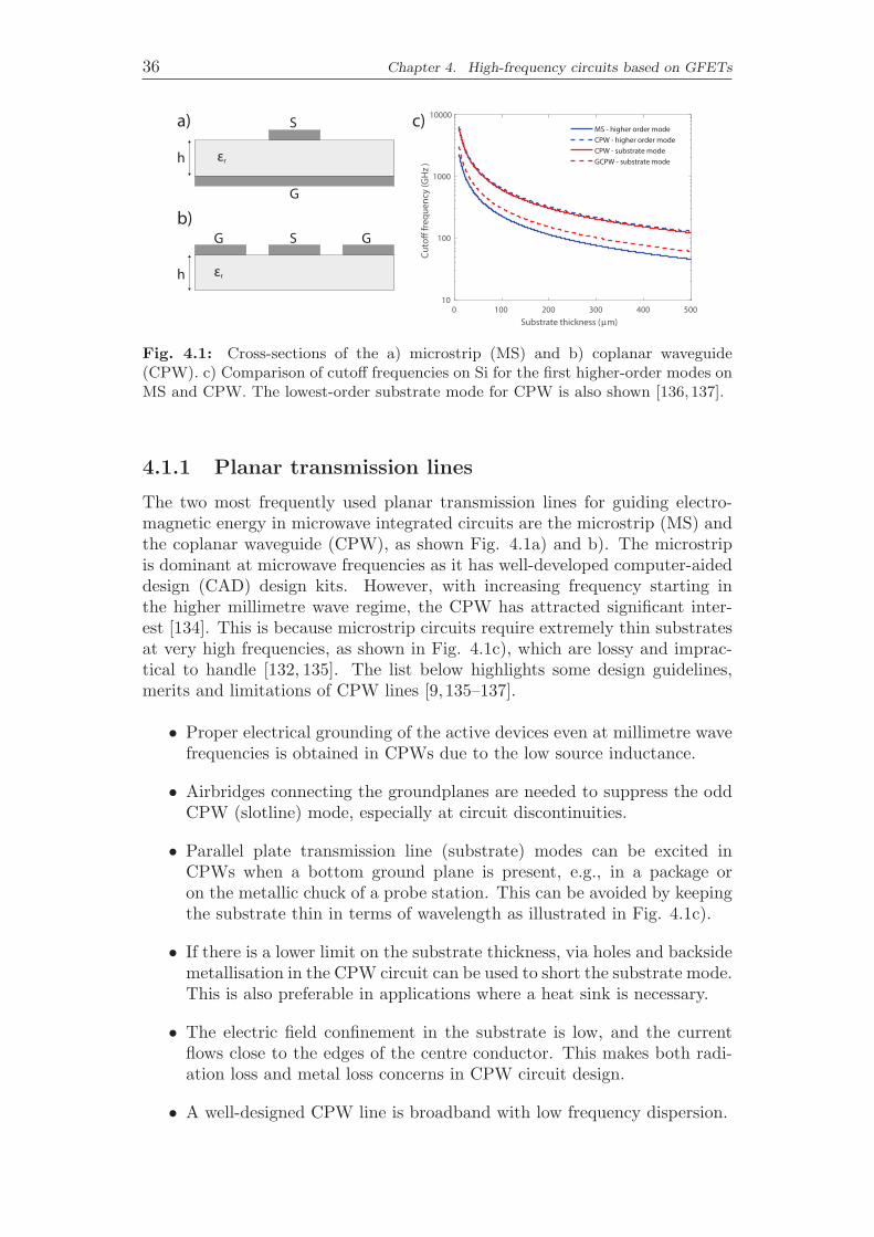
36 Chapter 4. High-frequency circuits based on GFETs
0 100 200 300 400 500
Substrate thickness (μm)
10
100
1000
10000
Cut
off fr
eque
ncy
(GH
z)
MS - higher order modeCPW - higher order modeCPW - substrate modeGCPW - substrate modeh
h
εr
εr
S
S
G
G G
a)
b)
c)
Fig. 4.1: Cross-sections of the a) microstrip (MS) and b) coplanar waveguide(CPW). c) Comparison of cutoff frequencies on Si for the first higher-order modes onMS and CPW. The lowest-order substrate mode for CPW is also shown [136,137].
4.1.1 Planar transmission lines
The two most frequently used planar transmission lines for guiding electro-magnetic energy in microwave integrated circuits are the microstrip (MS) andthe coplanar waveguide (CPW), as shown Fig. 4.1a) and b). The microstripis dominant at microwave frequencies as it has well-developed computer-aideddesign (CAD) design kits. However, with increasing frequency starting inthe higher millimetre wave regime, the CPW has attracted significant inter-est [134]. This is because microstrip circuits require extremely thin substratesat very high frequencies, as shown in Fig. 4.1c), which are lossy and imprac-tical to handle [132, 135]. The list below highlights some design guidelines,merits and limitations of CPW lines [9, 135–137].
• Proper electrical grounding of the active devices even at millimetre wavefrequencies is obtained in CPWs due to the low source inductance.
• Airbridges connecting the groundplanes are needed to suppress the oddCPW (slotline) mode, especially at circuit discontinuities.
• Parallel plate transmission line (substrate) modes can be excited inCPWs when a bottom ground plane is present, e.g., in a package oron the metallic chuck of a probe station. This can be avoided by keepingthe substrate thin in terms of wavelength as illustrated in Fig. 4.1c).
• If there is a lower limit on the substrate thickness, via holes and backsidemetallisation in the CPW circuit can be used to short the substrate mode.This is also preferable in applications where a heat sink is necessary.
• The electric field confinement in the substrate is low, and the currentflows close to the edges of the centre conductor. This makes both radi-ation loss and metal loss concerns in CPW circuit design.
• A well-designed CPW line is broadband with low frequency dispersion.

4.2. Small-signal GFET amplifiers 37
GFET
[S]
Input
matching
network
Output
matching
networkZ
0
Z0
ΓS Γout ΓLΓin
Psource Pload
Fig. 4.2: Schematic drawing of a single-stage small-signal GFET amplifier layout.
0 0.2 0.4 0.6 0.8 1 1.2 1.4 1.6
Frequency (GHz)
0
2
4
6
8
10
12
Gai
n (d
B)
Measurement - [Paper E ]Model - [Paper E ]Measurement - [Zhang 2016]Model - [Zhang 2016]Inductor R s = 5 Ω
1.49 mm
1.5
3 m
m
GFET
Spiral
inductor
a) b)
Fig. 4.3: a) Performance of small-signal GFET amplifiers using an exfoliated GFET(Lg = 1 μm, Wg = 2 × 30 μm) and a wire inductor [Paper E], as well as a CVDGFET (Lg = 1 μm, Wg = 2×120 μm) and a planar inductor [96]. The dashed blackline shows the CVD GFET matched with a similar but low-loss planar inductor.b) Micrograph of the planar amplifier with SEM image of the airbridges in the inset.
4.2 Small-signal GFET amplifiers
The value of fmax is the highest frequency at which a transistor can providepower gain under idealised conditions. Typically, however, values of fT andfmax should be several times higher than the intended application frequencyfor the device to exhibit gain at practical impedance levels. The actual gainof an amplifier is the so-called transducer power gain, which, at a certain biaspoint and from the S-parameter matrix at a certain frequency, is given by
GT =Pload
Psource=
1− |ΓS |2|1− ΓinΓS |2 |S21|2 1− |ΓL|2
|1− S22ΓL|2 . (4.1)
In Eq. 4.1, Γin is the reflection coefficient looking into the device input, whileΓS and ΓL are the reflection coefficients looking from the device towards thesource and load, as shown in Fig. 4.2. The stipulation that |S21| > 1 is animportant prerequisite to fabricate an amplifier. With the starting point of|S21|2, the amplifier gain is further enhanced by designing input and outputimpedance matching networks, which are quantified by the source and loadreflection coefficients, Γs and ΓL, respectively [138]. The matching networks

38 Chapter 4. High-frequency circuits based on GFETs
R S
C = 220 fF pp
L = 20 nH
C = 220 fF
Planar inductor equivalent circuit
0.2
0.5
1.0
2.0
5.0
+j0.2
-j0.2
+j0.5
-j0.5
+j1.0
-j1.0
+j2.0
-j2.0
+j5.0
-j5.0
0.0 ∞
Wire inductorPlanar inductorR s = 30 Ω (0.3μm Au)
R s = 5 Ω (2 μm Au)
Γ s @ 1 GHzWire
Planar
Fig. 4.4: Measured S-parameters up to 2 GHz for the surface mount wire inductor(L = 36 nH from the datasheet) [Paper E] and the planar inductor (L = 20 nH fromthe extracted equivalent circuit) [96]. A simulated planar inductor with thicker goldis included for comparison. The models were verified by EM simulation.
are implemented either by distributed transmission lines [125] or by lumpedinductors and capacitors, as is the case in [Paper E] using a surface mountinductor and in [30,96] using integrated planar inductors. Ideally, the matchingnetworks should be lossless.
4.2.1 Matching circuit design and performance
The first matched small-signal amplifier which exhibits substantial power gainat microwave frequencies was demonstrated in [Paper E]. Previously, onlyvoltage gain at gigahertz frequencies was reported [99]. After the publica-tion of [Paper E], several reports have appeared demonstrating power gainin integrated GFET amplifiers including a 4 dB gain achieved at 4.8 GHzusing a CVD GFET [30] and a 3.4 dB gain achieved at 14.3 GHz with anSiC GFET [125]. Moreover, in conjunction with [Paper C], CVD GFETs in-tegrated with planar inductors were fabricated. The results were presentedin [96] and are introduced for comparison to [Paper E] below.
In the low-GHz frequency range, the input impedance of the on-waferGFETs is inherently capacitive. Thus, the source reflection coefficient formaximum gain lies in the inductive half plane of the Smith Chart close to thatof an open circuit, ΓS≈ S∗
11 [Paper E]. On the other hand, the output imped-ance for relatively wide devices is reasonably close to 50 Ω, and the enhance-ment from drain matching is small when weighed against the increased circuitcomplexity. Discrete matching networks were chosen here since distributedmatching circuits on a silicon substrate would consume an impractically largearea at such a low frequency. A series inductor on the gate port is selected forsimultaneous matching and convenient DC biasing.
The first proof-of-concept amplifier in [Paper E] is based on an exfoli-ated graphene FET and a surface mount inductor. The second-generation

4.2. Small-signal GFET amplifiers 39
design from [96] realised with a CVD graphene FET uses an integrated on-chip matching inductor. This demonstrates a higher possible integration levelof the technology as we move towards the full wafer-scale. The performanceof the two amplifiers is compared in Fig. 4.3. Both designs use GFETs with1-μm-long gates, while the CVD device is considerably wider to accommo-date the lower normalised transconductance due to its thicker gate oxide. Thereduced gain for the CVD GFET is related to the high resistive loss of thefabricated planar inductor. This is identified using the inductor equivalentcircuit in Fig. 4.4. This shows the need for electroplating of ∼2 μm Au for thebottom metallisation of the inductor. The capacitive loss on the high-resistivesilicon is reasonably low. In this thesis, the active devices both operate with a6 - 10 dB gain at 1 GHz ≈ 0.1·fmax. Similarly, the recently demonstrated ICwith a 200-nm-gate SiC GFET can provide a lower 3.4 dB amplification closerto the limit frequency at 14.3 GHz ≈ 0.35 · fmax [125].
4.2.2 Analysis of the amplifier noise figure
The noise figure of the amplifier in [Paper E] at the design frequency of 1 GHzwas determined as NF = 6.4± 0.4 dB. The measurement was performed withthe Y-factor method, which by definition amounts to finding
Y =PH
PC=
TH + Tn
TC + Tn. (4.2)
The hot and cold noise powers, PH and PC , are measured at the output of thedevice while presenting the known hot and cold noise temperatures, TH andTC , at its input. The total noise temperature Tn is solved from Eq. 4.2. Todistinguish the device and measurement receiver noise figures, the device gainis de-embedded using the cascade formula [109]. The gain is measured via theoutput noise powers with the device and a through connection inserted in themeasurement path, GDUT = (P ′
H − P ′C)/(PH − PC).
To obtain the minimum noise figure of the GFET itself, the Pospieszalskinoise model was extracted for the complete amplifier. It was assumed in theextraction that Tg = Ta [139]. Thus, the measured amplifier noise figure at asingle source impedance at each frequency is enough for the extraction of thesecond frequency independent model parameter Td ≈ 23, 000 K. This value ofTd is significantly higher than values reported for other GFETs [140], [PaperF] as well as other FET technologies [112, 113]. Since a satisfactory fit wasobtained, this indicates the lumping of several noise mechanisms into the draincurrent source. However, gate leakage current, which can cause an increasednoise figure in this frequency range [123], was not observed. Instead, the likelycause of the high Td in [Paper E] is the omission of the substrate resistors Rpg
and Rpd. These have been shown to have a similar effect on the minimumnoise figure as a conducting gate in [Paper F]. Indeed, for the GFETs on semi-insulating SiC, lower expected values of Td< 2, 000 K were found even withoutthe inclusion of the substrate resistors in the model [124,140]. In addition, thelarge uncertainty in the extraction of the source resistance for an exfoliatedGFET propagates into the calculated value for Td. To summarise, the slopeof NFmin versus frequency in [Paper E] is likely overestimated.

40 Chapter 4. High-frequency circuits based on GFETs
Z0
Gate bias
LO filterRF filter
IF filter
Z0
Z0
fLO
PLO
fRF
PRF
a)
b)GFET
Z0
Gate bias
LO filter
RF filter
IF filter
Z0
Z0
fLO
PLO
GFET
fRF
PRF
Drain bias
Fig. 4.5: Schematic circuits for single-ended a) active and b) resistive GFET mixers.
4.3 Frequency mixers based on GFETs
There are two main operation modes of the frequency mixers shown in Fig. 4.5,the transconductance (active) mixer and the resistive (passive) mixer. In theactive mixer, the RF signal applied on the gate is mixed with an LO pumpedtransconductance waveform. In the resistive mixer, the drain-source resistanceis pumped and mixed with an RF signal applied at the drain. Moreover, themixers are divided into fundamental (fIF = fRF − fLO) and subharmonic(fIF = fRF −2fLO). The active mixer designs are often fundamental, whereasboth fundamental and subharmonic resistive mixers are commonly found. Inany case, all variants require filter circuitry to separate the LO, RF and IFsignal paths and to apply a DC gate bias. In addition, balanced designs canbe used for improved isolation and linearity [130]. The conversion loss of allthe down-converting resistive GFET mixers discussed below are compared inFig. 4.6 to those of other technologies. These results should be compared tothe theoretical minimum conversion loss of 3.9 dB in a resistive mixer [141].
4.3.1 Fundamental mixers
The reported active GFET mixers are limited by the small transconductanceand give CL > 14 dB up to 5 GHz [30,142]. Similarly, the best resistive GFETmixer also gives CL = 14 dB at 2 GHz and a comparable LO power level [143].However, these results should also be compared to GaAs FETs, which providea CG of ∼ 10 dB in the active mixer operation mode [130].
The IIP3 quality factor, Q(IIP3) = IIP3/PLO, is a useful parameter tocompare the linearity of different mixers. This is because an increased LOpower minimises the duration of the LO sweep where the mixer is close to thenonlinear turn-on region [144]. GaN power devices give high linearity but lowQ(IIP3) since they can withstand a very high LO power [145]. As predictedin Section 3.7.2, the fundamental GFET resistive mixers [143] outperform thesubharmonic counterparts [83] and [Paper D], and they are comparable toGaAs technology in terms of linearity, Q(IIP3) ∼ 20 dB [131].
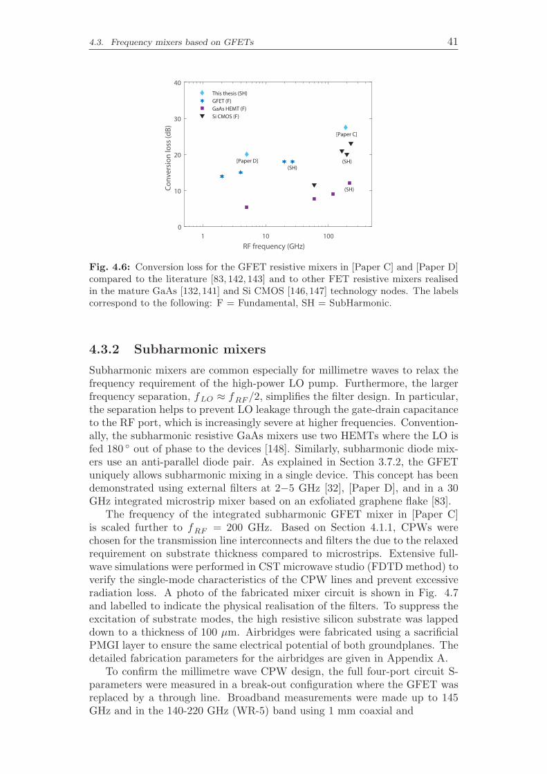
4.3. Frequency mixers based on GFETs 41
1 10 100
RF frequency (GHz)
0
10
20
30
40
Con
vers
ion
loss
(dB)
This thesis (SH)GFET (F)GaAs HEMT (F)Si CMOS (F)
[Paper D]
[Paper C]
(SH)
(SH)
(SH)
Fig. 4.6: Conversion loss for the GFET resistive mixers in [Paper C] and [Paper D]compared to the literature [83, 142, 143] and to other FET resistive mixers realisedin the mature GaAs [132,141] and Si CMOS [146,147] technology nodes. The labelscorrespond to the following: F = Fundamental, SH = SubHarmonic.
4.3.2 Subharmonic mixers
Subharmonic mixers are common especially for millimetre waves to relax thefrequency requirement of the high-power LO pump. Furthermore, the largerfrequency separation, fLO ≈ fRF /2, simplifies the filter design. In particular,the separation helps to prevent LO leakage through the gate-drain capacitanceto the RF port, which is increasingly severe at higher frequencies. Convention-ally, the subharmonic resistive GaAs mixers use two HEMTs where the LO isfed 180 ◦ out of phase to the devices [148]. Similarly, subharmonic diode mix-ers use an anti-parallel diode pair. As explained in Section 3.7.2, the GFETuniquely allows subharmonic mixing in a single device. This concept has beendemonstrated using external filters at 2−5 GHz [32], [Paper D], and in a 30GHz integrated microstrip mixer based on an exfoliated graphene flake [83].
The frequency of the integrated subharmonic GFET mixer in [Paper C]is scaled further to fRF = 200 GHz. Based on Section 4.1.1, CPWs werechosen for the transmission line interconnects and filters the due to the relaxedrequirement on substrate thickness compared to microstrips. Extensive full-wave simulations were performed in CST microwave studio (FDTD method) toverify the single-mode characteristics of the CPW lines and prevent excessiveradiation loss. A photo of the fabricated mixer circuit is shown in Fig. 4.7and labelled to indicate the physical realisation of the filters. To suppress theexcitation of substrate modes, the high resistive silicon substrate was lappeddown to a thickness of 100 μm. Airbridges were fabricated using a sacrificialPMGI layer to ensure the same electrical potential of both groundplanes. Thedetailed fabrication parameters for the airbridges are given in Appendix A.
To confirm the millimetre wave CPW design, the full four-port circuit S-parameters were measured in a break-out configuration where the GFET wasreplaced by a through line. Broadband measurements were made up to 145GHz and in the 140-220 GHz (WR-5) band using 1 mm coaxial and
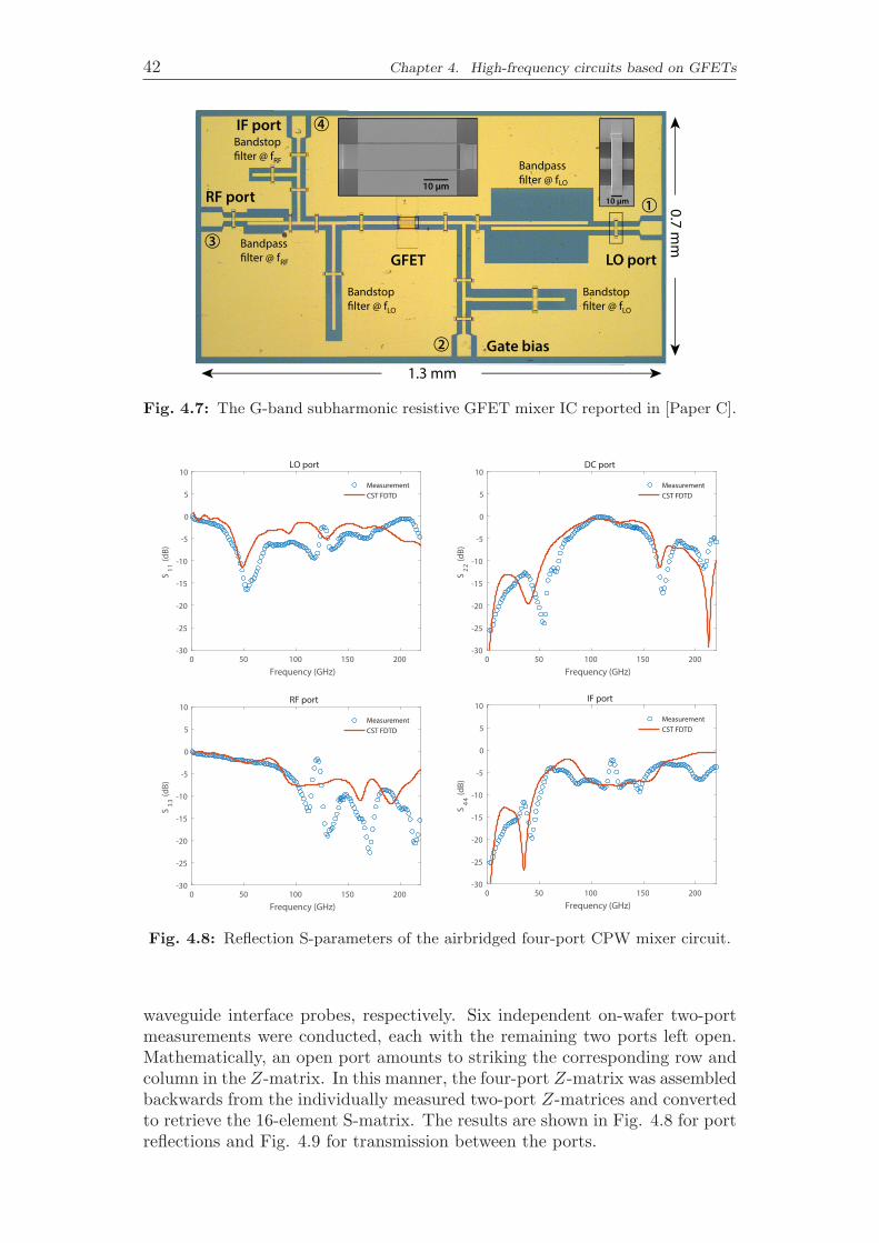
42 Chapter 4. High-frequency circuits based on GFETs
RF port
IF port
LO port
Gate bias
GFET
1.3 mm
0.7
mm
Bandpass
filter @ fLO
Bandpass
filter @ fRF
Bandstop
filter @ fLO
Bandstop
filter @ fLO
Bandstop
filter @ fRF
10 μm
10 μm 1
2
3
4
Fig. 4.7: The G-band subharmonic resistive GFET mixer IC reported in [Paper C].
0 50 100 150 200
Frequency (GHz)
-30
-25
-20
-15
-10
-5
0
5
10
S1
1 (d
B)
LO port
MeasurementCST FDTD
0 50 100 150 200
Frequency (GHz)
-30
-25
-20
-15
-10
-5
0
5
10
S2
2 (d
B)DC port
MeasurementCST FDTD
0 50 100 150 200
Frequency (GHz)
-30
-25
-20
-15
-10
-5
0
5
10
S3
3 (d
B)
RF port
MeasurementCST FDTD
0 50 100 150 200
Frequency (GHz)
-30
-25
-20
-15
-10
-5
0
5
10
S4
4 (d
B)
IF port
MeasurementCST FDTD
Fig. 4.8: Reflection S-parameters of the airbridged four-port CPW mixer circuit.
waveguide interface probes, respectively. Six independent on-wafer two-portmeasurements were conducted, each with the remaining two ports left open.Mathematically, an open port amounts to striking the corresponding row andcolumn in the Z-matrix. In this manner, the four-port Z-matrix was assembledbackwards from the individually measured two-port Z-matrices and convertedto retrieve the 16-element S-matrix. The results are shown in Fig. 4.8 for portreflections and Fig. 4.9 for transmission between the ports.

4.3. Frequency mixers based on GFETs 43
Finally, the on-wafer mixer conversion loss was measured to be 29 ± 2 dBwithin the RF frequency interval 185-210 GHz using the setup in Fig. 4.10. Toimprove the conversion loss, the pumped GFET resistance should resemble asquare wave with a higher on-off ratio and even on- and off-state times, i.e., abandgap is required for graphene. However, even in the absence of a bandgap,improved mobility and contact resistance would be advantageous in the GFETresistive mixer to reduce the LO power required to switch between the on- andoff-states. In addition, a receiver design was fabricated where the mixer in Fig.4.7 was cascaded with the IF amplifier in Fig. 4.3 via a DC block capacitor.However, no functioning circuit could be measured due to the low GFET yield.
0 50 100 150 200
Frequency (GHz)
-60
-50
-40
-30
-20
-10
0
10
S2
1 (d
B)
LO port - DC port
MeasurementCST FDTD
0 50 100 150 200
Frequency (GHz)
-60
-50
-40
-30
-20
-10
0
10
S3
1 (d
B)
LO port - RF port
MeasurementCST FDTD
0 50 100 150 200
Frequency (GHz)
-60
-50
-40
-30
-20
-10
0
10
S4
1 (d
B)
LO port - IF port
MeasurementCST FDTD
0 50 100 150 200
Frequency (GHz)
-60
-50
-40
-30
-20
-10
0
10
S3
2 (d
B)
RF port - DC port
MeasurementCST FDTD
0 50 100 150 200
Frequency (GHz)
-60
-50
-40
-30
-20
-10
0
10
S4
3 (d
B)
RF port - IF port
MeasurementCST FDTD
0 50 100 150 200
Frequency (GHz)
-60
-50
-40
-30
-20
-10
0
10
S4
2 (d
B)
DC port - IF port
MeasurementCST FDTD
Fig. 4.9: Transmission S-parameters of the airbridged four-port CPW mixer circuit.
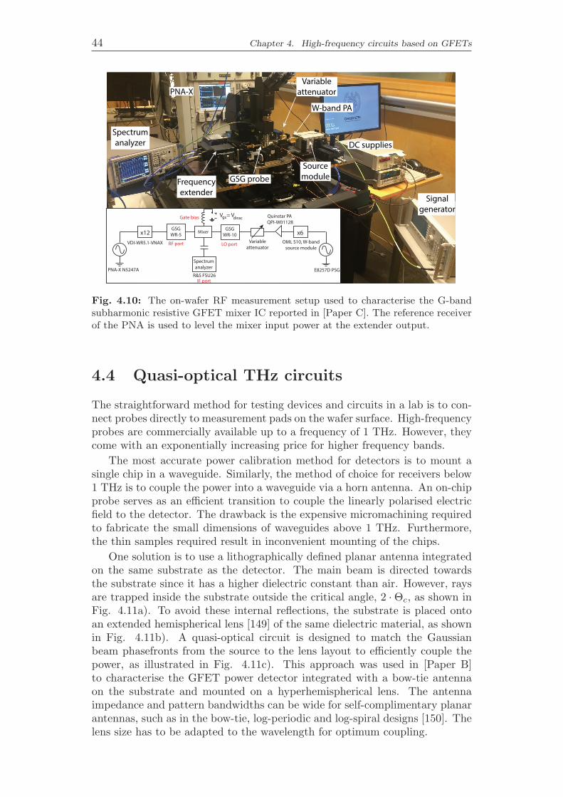
44 Chapter 4. High-frequency circuits based on GFETs
Signal
generator
DC supplies
PNA-X
Spectrum
analyzer
Frequency
extender
Source
module
W-band PA
E8257D PSG
GSG
WR-10 x6
OML S10, W-band
source module
Quinstar PA
QPI-W01128
GSG
WR-5x12
VDI-WR5.1-VNAX
PNA-X N5247A
Mixer
V = V
LO portRF port
Spectrum
analyzer
R&S FSU26
IF port
Gate bias gs dirac
Variable
attenuator
Variable
attenuator
GSG probe
Fig. 4.10: The on-wafer RF measurement setup used to characterise the G-bandsubharmonic resistive GFET mixer IC reported in [Paper C]. The reference receiverof the PNA is used to level the mixer input power at the extender output.
4.4 Quasi-optical THz circuits
The straightforward method for testing devices and circuits in a lab is to con-nect probes directly to measurement pads on the wafer surface. High-frequencyprobes are commercially available up to a frequency of 1 THz. However, theycome with an exponentially increasing price for higher frequency bands.
The most accurate power calibration method for detectors is to mount asingle chip in a waveguide. Similarly, the method of choice for receivers below1 THz is to couple the power into a waveguide via a horn antenna. An on-chipprobe serves as an efficient transition to couple the linearly polarised electricfield to the detector. The drawback is the expensive micromachining requiredto fabricate the small dimensions of waveguides above 1 THz. Furthermore,the thin samples required result in inconvenient mounting of the chips.
One solution is to use a lithographically defined planar antenna integratedon the same substrate as the detector. The main beam is directed towardsthe substrate since it has a higher dielectric constant than air. However, raysare trapped inside the substrate outside the critical angle, 2 ·Θc, as shown inFig. 4.11a). To avoid these internal reflections, the substrate is placed ontoan extended hemispherical lens [149] of the same dielectric material, as shownin Fig. 4.11b). A quasi-optical circuit is designed to match the Gaussianbeam phasefronts from the source to the lens layout to efficiently couple thepower, as illustrated in Fig. 4.11c). This approach was used in [Paper B]to characterise the GFET power detector integrated with a bow-tie antennaon the substrate and mounted on a hyperhemispherical lens. The antennaimpedance and pattern bandwidths can be wide for self-complimentary planarantennas, such as in the bow-tie, log-periodic and log-spiral designs [150]. Thelens size has to be adapted to the wavelength for optimum coupling.

4.5. Electrical model for FET THz detectors 45
Air
Air
Substrate
Antenna
2ΘcTrapped ray
Air
Substrate
Antenna
Hyperhemispherical lens
L=R/εr1/2
a)
b)
c)
Source
Paraboloidal mirror
Lens
Si lens
Lα
Antenna
Fig. 4.11: a) Planar antenna radiating on a substrate illustrating the trapped rays.b) The same planar antenna on a hyperhemispherical lens to prevent reflected rays.c) Quasi-optical circuit used to match the Gaussian beam wavefront from the sourceto the lens [Paper B]. The inset shows the bow-tie angle α and the bow-tie length L.
The bow-tie antenna from [Paper B] is illustrated in the inset of Fig. 4.11c).The outer and inner dimensions yield the upper and lower frequency limits,respectively, while the angle defines the real part of the antenna impedance.The simulated impedance in the lower frequency range of Fig. 4.12a) showsthat this particular design is electrically small at 600 GHz. An electricallylonger bow-tie has an off-broadside radiation pattern on an infinitely thickdielectric substrate [151]. However, the radiation pattern of an electricallyshort bow-tie on an infinite substrate resembles that of the simple dipole.This is then steered further towards the perpendicular direction by using thelens. The high simulated directivity from CST is illustrated in Fig. 4.12b)using a hyperhemispherical lens with a diameter d = 5 mm.
4.5 Electrical model for FET THz detectors
The plasma-wave theory has been predominantly used to explain the powerdetection in FETs [152]. The experimental FET detectors are said to operatein the so-called broadband detection regime, where a weak gate length anda strong mobility dependence on the NEP is suggested. Moreover, the the-ory indicates that the NEP decreases at high frequency where the plasmoniceffect is stronger. The plasmon effects might play a role in dedicated devicestructures. However, the NEP compilation in Fig. 4.13 displays no clear-cutsensitivity enhancement in high mobility III-V heterostructures compared toCMOS. Furthermore, there is roughly a NEP ∝ f2 trend at high frequencies.
To address these discrepancies between theory and experiment, the Volterra-based electrical model in [Paper A] was developed. It clarifies the influence ofmobility and RF frequency on the NEP and was used to derive device designrules, both under conjugately matched conditions and when Rj � Z0. Here,Rj = 1/gd1 is the real part of the small-signal FET impedance. This situationis typical for detectors fed by standard probe and antenna impedances, and itis therefore used as the example in the discussion below.
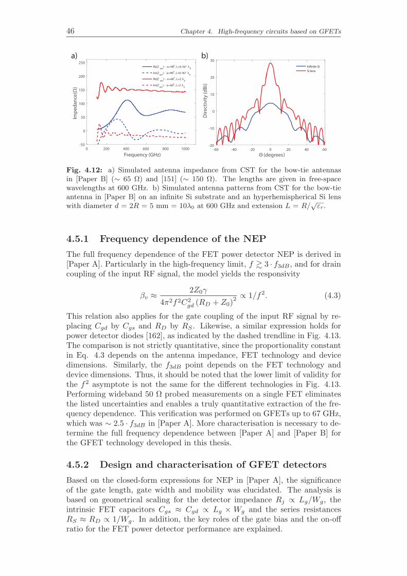
46 Chapter 4. High-frequency circuits based on GFETs
0 200 400 600 800 1000
Frequency (GHz)
-50
0
50
100
150
200
250
Impe
danc
e (Ω
)
Re(Zant
) - α=90 , L=0.167 λ0
Im(Zant
) - α=90 , L=0.167 λ0
Re(Zant
) - α=60 , L=2 λ0
Im(Zant
) - α=60 , L=2 λ0
-60 -40 -20 0 20 40 60
Θ (degrees)
-20
-10
0
10
20
30
Dire
ctiv
ity (d
Bi)
Infinite SiSi lens
a) b)
Fig. 4.12: a) Simulated antenna impedance from CST for the bow-tie antennasin [Paper B] (∼ 65 Ω) and [151] (∼ 150 Ω). The lengths are given in free-spacewavelengths at 600 GHz. b) Simulated antenna patterns from CST for the bow-tieantenna in [Paper B] on an infinite Si substrate and an hyperhemispherical Si lenswith diameter d = 2R = 5 mm = 10λ0 at 600 GHz and extension L = R/
√εr.
4.5.1 Frequency dependence of the NEP
The full frequency dependence of the FET power detector NEP is derived in[Paper A]. Particularly in the high-frequency limit, f � 3 · f3dB , and for draincoupling of the input RF signal, the model yields the responsivity
βv ≈ 2Z0γ
4π2f2C2gd (RD + Z0)
2 ∝ 1/f2. (4.3)
This relation also applies for the gate coupling of the input RF signal by re-placing Cgd by Cgs and RD by RS . Likewise, a similar expression holds forpower detector diodes [162], as indicated by the dashed trendline in Fig. 4.13.The comparison is not strictly quantitative, since the proportionality constantin Eq. 4.3 depends on the antenna impedance, FET technology and devicedimensions. Similarly, the f3dB point depends on the FET technology anddevice dimensions. Thus, it should be noted that the lower limit of validity forthe f2 asymptote is not the same for the different technologies in Fig. 4.13.Performing wideband 50 Ω probed measurements on a single FET eliminatesthe listed uncertainties and enables a truly quantitative extraction of the fre-quency dependence. This verification was performed on GFETs up to 67 GHz,which was ∼ 2.5 · f3dB in [Paper A]. More characterisation is necessary to de-termine the full frequency dependence between [Paper A] and [Paper B] forthe GFET technology developed in this thesis.
4.5.2 Design and characterisation of GFET detectors
Based on the closed-form expressions for NEP in [Paper A], the significanceof the gate length, gate width and mobility was elucidated. The analysis isbased on geometrical scaling for the detector impedance Rj ∝ Lg/Wg, theintrinsic FET capacitors Cgs ≈ Cgd ∝ Lg × Wg and the series resistancesRS ≈ RD ∝ 1/Wg. In addition, the key roles of the gate bias and the on-offratio for the FET power detector performance are explained.
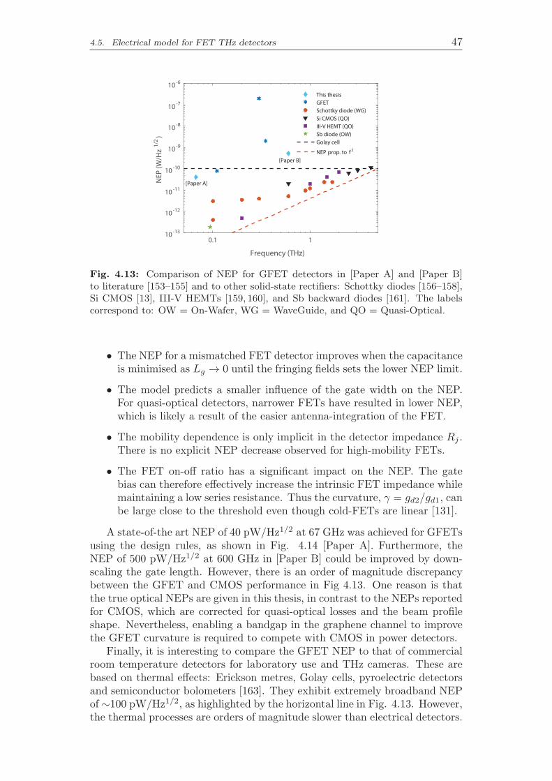
4.5. Electrical model for FET THz detectors 47
0.1 1
Frequency (THz)
10 -13
10 -12
10 -11
10 -10
10 -9
10 -8
10 -7
10 -6
NEP
(W/H
z1/
2)
This thesisGFETSchottky diode (WG)Si CMOS (QO)III-V HEMT (QO)Sb diode (OW)Golay cell
NEP f 2prop. to
[Paper A]
[Paper B]
Fig. 4.13: Comparison of NEP for GFET detectors in [Paper A] and [Paper B]to literature [153–155] and to other solid-state rectifiers: Schottky diodes [156–158],Si CMOS [13], III-V HEMTs [159, 160], and Sb backward diodes [161]. The labelscorrespond to: OW = On-Wafer, WG = WaveGuide, and QO = Quasi-Optical.
• The NEP for a mismatched FET detector improves when the capacitanceis minimised as Lg → 0 until the fringing fields sets the lower NEP limit.
• The model predicts a smaller influence of the gate width on the NEP.For quasi-optical detectors, narrower FETs have resulted in lower NEP,which is likely a result of the easier antenna-integration of the FET.
• The mobility dependence is only implicit in the detector impedance Rj .There is no explicit NEP decrease observed for high-mobility FETs.
• The FET on-off ratio has a significant impact on the NEP. The gatebias can therefore effectively increase the intrinsic FET impedance whilemaintaining a low series resistance. Thus the curvature, γ = gd2/gd1, canbe large close to the threshold even though cold-FETs are linear [131].
A state-of-the art NEP of 40 pW/Hz1/2 at 67 GHz was achieved for GFETsusing the design rules, as shown in Fig. 4.14 [Paper A]. Furthermore, theNEP of 500 pW/Hz1/2 at 600 GHz in [Paper B] could be improved by down-scaling the gate length. However, there is an order of magnitude discrepancybetween the GFET and CMOS performance in Fig 4.13. One reason is thatthe true optical NEPs are given in this thesis, in contrast to the NEPs reportedfor CMOS, which are corrected for quasi-optical losses and the beam profileshape. Nevertheless, enabling a bandgap in the graphene channel to improvethe GFET curvature is required to compete with CMOS in power detectors.
Finally, it is interesting to compare the GFET NEP to that of commercialroom temperature detectors for laboratory use and THz cameras. These arebased on thermal effects: Erickson metres, Golay cells, pyroelectric detectorsand semiconductor bolometers [163]. They exhibit extremely broadband NEPof ∼100 pW/Hz1/2, as highlighted by the horizontal line in Fig. 4.13. However,the thermal processes are orders of magnitude slower than electrical detectors.

48 Chapter 4. High-frequency circuits based on GFETs
10 20 30 40 50 60 70
Frequency (GHz)
10 -12
10 -11
10 -10
10 -9
10 -8
NEP
(W/H
z1/2
)
NEP 50Ω
Model [Paper A]
NEP 50Ω × (1-|S 22 |2 )
Model [Paper A]
-4 -3 -2 -1
Vgs -Vdirac (V)10-11
10-10
10-9
10-8
NEP
50Ω
(W/H
z1/2
)
0 1 2
Measurement
Model [Paper A]
Fig. 4.14: The Volterra model agreement of NEP for a GFET (Lg = 0.5 μm andWg = 2× 1.25 μm) versus frequency and gate voltage (in the inset) [Paper A].
4.6 Graphene antennas for energy harvesting
In addition to high data rate communications links, the Internet of thingsis an essential part of the next generation mobile networks. Specifically, themachine-to-machine (M2M) communication of sensor readings is predicted totake place on a massive scale to monitor and control the status of objectsand people. The deployment and maintenance of the sensors are requiredto be cheap and eco-friendly, which means that they must be operated self-sustainable instead of relying on battery power. One option for ubiquitoussensor deployment in urban environments is to harvest RF energy. However,new materials are required to realise the omnipresent Internet of things. Inparticular, transparent and flexible antennas would enable a diversity of M2Mapplications, e.g., on windows, or for wearable devices.
This was the motivation to evaluate the prospects of using graphene dipoleantennas to harvest RF energy for self-sustainable M2M sensors in [Paper I].The graphene antenna efficiency was simulated in Ansys HFSS, and translatedto the harvested power based on experimental ambient RF power levels [164].Finally, the harvested power was subtracted from the transmitter DC powerconsumptions of a current state-of-the-art commercial transceiver [165], and anultra-low-power transceiver demonstrated at a research institution [166]. Thedependence of the transceiver net power consumption on the graphene antennasheet resistance is shown in Fig. 4.15, under the M2M assumption of onesensor status transmission per day. Conclusions for the two most interestingcombinations of available power and power consumption are listed below.
• On a location with average RF intensity, SBA, the low-power transceiverand graphene Rsh < 100 Ω/sq are required for self-sustainable operation.
• On a location with maximum RF intensity, SBA, the commercial transceiverand graphene Rsh < 5 Ω/sq are required for self-sustainable operation.

4.6. Graphene antennas for energy harvesting 49
0.01 0.1 1 10 100
Sheet resistance (Ω/sq)
-2
0
2
4
6
8
10
12
14
Net
pow
er c
onsu
mpt
ion
(μW
)
Tirronen PDC
- Average SBA
Mercier PDC
- Average SBA
Tirronen PDC
- Maximum SBA
Break even
1 10
Sheet resistance (Ω/sq)
-0.4
-0.3
-0.2
-0.1
0
0.1
Net
pow
er c
onsu
mpt
ion
(μW
)
50 5
Fig. 4.15: The net power consumption of the transceiver assuming a single datatransmission event per day [Paper I]. Energy is harvested in the communicationfrequency bands around 2 GHz using a graphene dipole antenna.
As summarised in Section 3.2.2, special treatments can only reduce themultilayer CVD graphene sheet resistance to ∼20 Ω/sq. Thus, transparentantennas with sufficient efficiency for self-sustainable sensors is currently avery challenging task, given the available ambient RF power and DC powerconsumption of transmitters for M2M systems. Nevertheless, the cost andflexibility advantages from ink-jet printed, opaque graphene might be used.

50 Chapter 4. High-frequency circuits based on GFETs

Chapter 5
Conclusions and futureoutlook
The objective of this thesis was to advance wafer-scale graphene technologyfor microwave and THz applications. To this end, fabrication, characterisationand modelling of CVD GFETs on silicon substrates for RF applications wereconducted to identify the performance limits of the technology. Furthermore,both the integrated 200 GHz subharmonic mixer circuit and the 600 GHzquasi-optical power detector are state-of-the-art GFET demonstrators.
Today, the GFET THz detector operation is ascribed to overdamped plasma-waves. The take-home message of the plasma-wave theory is that a high car-rier mobility is the most important factor for sensitive detection. However, theGFET power detector in [Paper B] performs an order of magnitude worse thanits CMOS counterparts despite the higher mobility. The electrical model forFET power detectors in [Paper A] aims to explain this discrepancy. Contraryto previous models, the missing bandgap rather than the mobility is the keyto understanding the inferior GFET detector. Since it is based on the lumpedlarge-signal FET equivalent circuit, the model lends itself to the derivation ofclosed-form expressions for the NEP in the intrinsic capacitances and parasiticresistances. In contrast to the plasma-wave picture, these equations reveal aninverse gate length and frequency dependence of the NEP.
Similar to the power detectors, the high conversion loss of the passiveGFET resistive subharmonic mixers in [Paper C] and [Paper D] is not due tothe low mobility. This only increases the demand on the LO sweep power topump the mixer between the on- and off-states. Instead, the ultimate problemsfor fundamental and subharmonic resistive GFET mixers reside in the highseries resistance and the missing graphene bandgap, which limit the on- andoff-states, respectively. The methods of establishing a bandgap in graphenesimultaneously degrade the mobility. This is unfortunate for active GFETs,which require both a sizeable bandgap and a high mobility. However, evena bandgap at reduced mobility is a major progress step for the performanceof both GFET power detectors and mixers. Furthermore, the subharmonicGFET mixers require the gate to be biased at the Dirac voltage. Under thisbias condition, higher levels of third-order intermodulation are generated thanin fundamental resistive mixers operated for minimum conversion loss.
51

52 Chapter 5. Conclusions and future outlook
Contrary to passive applications, high mobility is the key to higher trans-conductance in active GFETs. Together with a bandgap to reduce the outputconductance this is required to maximise the cutoff frequency and maximumfrequency of oscillation, for which a vast amount of experimental data exists.However, knowledge of the microwave noise performance of active GFETs isequally important for the design of LNAs in receiver circuits. For the firsttime, the full GFET noise parameters are reported in [Paper F]. This enablesthe construction of the Pospieszalski and PRC noise models. Similar to thecase of oxide-gated silicon MOSFETs, a low correlation factor is extracted inthe PRC model for the gate and drain noise sources. Future studies have tofully clarify whether the correlation factor can be improved by higher qual-ity gate stacks on graphene or if the low correlation factor is a limitation ofthe GFET device structure. Additionally, better gate stacks would improvethe CVD GFET mobility. In other words, it is necessary to elucidate if boththe
√Ids/gm ratio and the correlation factor in GFETs can compete with the
values observed for III-V HEMTs.Currently, replacements to both the bottom- and top-gate graphene-oxide
interfaces are developed to improve the carrier mobility for active CVDGFETs.The h-BN dielectric environment is optimal for high-mobility graphene on thescale of exfoliated flakes. However, there are no procedures for high-qualitylayer-by-layer transfer or in situ growth of large-area h-BN and CVD grapheneon a technologically relevant scale. The development of the h-BN technologyis especially important for realising low-noise GFETs. Moreover, by screeningthe charged impurities using high-κ ferroelectrics is effective to improve themobility only in dirty graphene samples from inherently low levels [Paper H].
In addition to the bandgap and mobility issues, the high contact resistanceis often highlighted as a major obstacle for GFET technology in RF electron-ics. The bottlenecks of metal contacts have been identified to a large extent.However, in CVD graphene processing there is poor reproducibility [Paper G].A high contact resistance deteriorates the resistive mixer conversion loss, thedetector noise equivalent power and the amplifier noise figure [Paper E].
Presently, epitaxial GFETs show more reproducible mobility and contactresistance, and they are more promising than CVD GFETs for high-end RFcircuits. In addition, hydrogen-intercalated bilayer graphene on SiC exhibitsa small bandgap induced by the built-in field in the substrate. Still, there is alarge gap in its performance compared to even silicon microwave FETs.
Therefore, the most likely opportunities for CVD graphene are in appli-cations where current technology performs poorly, in particular, for flexibleelectronics. For instance, the potential of graphene antennas for deploymentin a ubiquitous Internet of things scenario is investigated in [Paper I]. In thiscontext, the inherent versatility in the transfer of CVD graphene to arbi-trary substrates is a decisive factor. Consequently, the CVD GFET circuitson silicon presented in this thesis can be viewed as the preamble for flexiblegraphene-based terahertz electronics. In addition, the CVD graphene has ahigher potential than SiC graphene for high-end RF GFETs given a significantbreakthrough in the growth of graphene and boron nitride heterostructures.

Chapter 6
Summary of appendedpapers
This chapter presents a brief summary of the content of the appended papersand a short description of my contribution to each paper.
Paper A
An Accurate Empirical Model Based on Volterra Series for FETPower Detectors
In this paper an empirical and equivalent circuit based model for FET powerdetectors was presented and experimentally verified by measurements on GFETs.Main results are the closed-form expressions for the detector responsivity andnoise equivalent power and the dimensional scaling rules.
My contributions: Initiated the work and derived the model equations. Thendesigned, fabricated and characterised the devices to assess the model validity.Interpreted the results and wrote the paper.
Paper B
Antenna-Integrated 0.6 THz FET Direct Detectors Based on CVDGraphene
In this paper a state-of-the-art quasi-optical GFET power detector with noiseequivalent power of 500 pW/Hz1/2 at 600 GHz is demonstrated.
My contributions: Main responsible for the device fabrication. Participatedwith co-authors in the design, characterisation and writing of the paper.
Paper C
A 185-215 GHz Subharmonic Resistive Graphene FET IntegratedMixer on Silicon
In this paper the a record high frequency for integrated graphene electronicsis shown. The results show state-of-the-art performance in terms of bothconversion loss and operating frequency.
53

54 Chapter 6. Summary of appended papers
My contributions: Main responsible for the circuit fabrication scheme andthe millimetre wave characterisation. Provided regular input during the circuitdesign phase and took a leading role in the writing of the paper.
Paper D
Resistive Graphene FET Subharmonic Mixers: Noise and LinearityAssessment
In this paper the conversion loss, noise figure and linearity of GFET resistivemixers in the 2-5 GHz frequency range are reported.
My contributions: Performed the fabrication, characterisation and analysistogether with co-authors. Main responsible for writing the paper.
Paper E
10-dB small-signal graphene FET amplifier
In this paper the first GFET amplifier with 10 dB gain and 6.4 dB noise figureis reported, fabricated on exfoliated graphene. Tentative noise modelling basedon the Pospieszalski model is performed.
My contributions: Suggested the concept, performed the fabrication andnoise modelling. Took part in the characterisation and wrote the letter.
Paper F
Microwave noise characterization of graphene field effect transistors
In this paper the source-pull noise figure results on a GFET were presented.After de-embedding the parasitics from the noise parameters, the possibilityof 1-dB noise figure up to 2 GHz was predicted.
My contributions: Main responsible for arranging the noise measurements.Provided daily input during the phases of fabrication, data analysis and noisemodel development. Took a significant role in the writing of the paper.
Paper G
Microwave characterization of Ti/Au-graphene contacts
In this paper microwave measurements on circular TLM structures are usedto model the capacitance associated with the metal-graphene contact.
My contributions: Fabricated and measured the test structures. Performedthe data interpretation together with co-authors and wrote the paper.
Paper H
Effect of ferroelectric substrate on carrier mobility in graphene field-effect transistors
In this paper a mobility enhancement on LiNbO3 by screening of chargedimpurity is found at levels below 1,000 cm2/Vs. Moreover, gate oxide qualityis correlated to the graphene mobility via the microwave loss tangent.

55
My contributions: Participated in the fabrication and provided feedbackduring the data analysis and paper writing.
Paper I
Feasibility of Ambient RF Energy Harvesting for Self-SustainableM2M Communications Using Transparent and Flexible GrapheneAntennas
In this paper power budget calculations were performed to assess the viabilityof using transparent and flexible graphene antennas to harvest RF energy topower sensors in ubiquitous use cases in the future Internet of things.
My contributions: Responsible for a major part of the literature study,coordinated the calculations with input from the co-authors and wrote the paper.

56 Chapter 6. Summary of appended papers

Appendix A
Recipe CVD GFET circuits
The fabrication steps assumes the grown CVD graphene is transferred to a10×10 mm2 or 20×20 mm2 high resistivity Si chip with alignment marks.
1 Mesa and nanoconstriction etch
• Spin coat the negative tone ma-N 2401 resist undilutedat 3000 rpm during 30 s for 100 nm thickness.
• Soft bake on hotplate at 110 ◦C for 60 s.
• E-beam expose pattern proximity corrected using BEAMERat 100 kV/2 nA with a dose of 400 μC/cm2.
• Develop for 30 s in MF-CD-26, rinse DI, N2 blow dry.
• Resist ash at 50 W RF power/250 mTorr pressure for 5 s.
• Etch graphene at 50 W RF power/50 mTorr pressure for 6 s.
• Ash top resist at 50 W RF power/250 mTorr pressure for 3 s.
• Strip resist in acetone for 5 min at 19 ◦C, rinse IPA, N2 blow dry.
2 Ohmic contact metallisation
• Spin coat copolymer resist diluted in ethyl lactate (10% w/w)at 3000 rpm during 60 s for 400 nm thickness.
• Soft bake on hotplate at 170 ◦C for 5 min.
• Spin coat AR-P 6200.13 resist diluted 1:2 in anisole (4.3% w/w)at 4000 rpm during 60 s for 70 nm thickness.
• Soft bake on hotplate at 170 ◦C for 5 min.
• E-beam expose pattern proximity corrected using BEAMERat 100 kV/10 nA with a dose of 350 μC/cm2.
• Develop AR-P for 45 s in n-Amylacetate, N2 blow dry.
• Develop copolymer for 2 min in MIBK:IPA 1:1, N2 blow dry.
• Evaporate 1 nm Ti/15 nm Pd/100 nm Au.
• Lift-off in acetone for 10 min at 70 ◦C, rinse IPA, N2 blow dry.
57

58 Appendix A. Recipe CVD GFET circuits
3 Gate oxide formation
• Anneal in 1000 sccm Ar gas flow for 15 min at 230 ◦C.
• Evaporate 1 nm Al, oxidise on hotplate at 170 ◦C, repeat 4 times.
• Thermal ALD of 176 cycles at 300 ◦C for 15 nm Al2O3.
4 Gate finger metallisation
• Spin coat, bake, expose and develop according to step 2 .
• Evaporate 250 nm Al/10 nm Ti/50 nm Au.
• Lift-off in remover mr-Rem 400 for 15 min at 50 ◦C,rinse acetone and IPA, N2 blow dry.
5 Oxide etch to access ohmic metal layer
• Spin coat S1813 resist at 4000 rpm/30 s for 1.3 μm thickness.
• Soft bake on hotplate at 110 ◦C for 2 min.
• Expose direct laser writer, intensity 100% and focus offset 0%.
• Develop for 60 s in MF319, rinse DI, N2 blow dry.
• Resist ash at 50 W RF power/250 mTorr pressure for 30 s.
• Buffered oxide etch (7:1) dip for 30 s, rinse DI, N2 blow dry.
• Ash at 50 W RF power/250 mTorr pressure for 30 s.
• Strip resist in acetone at 70 ◦C for 5 min.
6 Pad and/or antenna metallisation(feature sizes � 5 μm, Au thickness � 300 nm)
• Dehydration bake on hotplate at 200 ◦C for 2 min.
• Spin coat HMDS adhesion promoter at 3000 rpm/30 s.
• Spin coat LOR 3B at 4000 rpm/60 s for 400 nm thickness.
• Soft bake on hotplate 200 ◦C for 5 min.
• Spin coat S1805 resist at 4000 rpm/60 s for 500 nm thickness.
• Soft bake on hotplate at 110 ◦C for 60 s.
• Expose direct laser writer, intensity 70% and focus offset 0%.
• Develop S1805 and etch < 1 μm undercut in LOR by MF319starting with 30 s, rinse DI, N2 blow dry.
• Resist ash at 50 W RF power/250 mTorr pressure for 10 s.
• Evaporate 10 nm Ti/300 nm Au.
• Lift-off in remover 1165 (or mr-Rem 400) for 15 min at 50 ◦C,rinse acetone and IPA, N2 blow dry.

59
7 Coplanar waveguide circuit metallisation(feature sizes � 5 μm, Au thickness � 500 nm)
• Spin coat copolymer resist diluted in ethyl lactate (10% w/w)at 5000 rpm during 60 s for 300 nm thickness.
• Soft bake on hotplate at 170 ◦C for 5 min.
• Spin coat copolymer resist diluted in ethyl lactate (10% w/w)at 3000 rpm during 60 s for 400 nm thickness.
• Soft bake on hotplate at 170 ◦C for 5 min.
• Spin coat AR-P 6200.13 resist diluted 1:2 in anisole (4.3% w/w)at 4000 rpm during 60 s for 70 nm thickness.
• Soft bake on hotplate at 170 ◦C for 5 min.
• E-beam expose pattern proximity corrected using BEAMERat 100 kV/35 nA with a dose of 350 μC/cm2.
• Develop AR-P for 45 s in n-Amylacetate, N2 blow dry.
• Develop copolymer for 2 min in MIBK:IPA 1:1, N2 blow dry.
• Resist ash at 50 W RF power/250 mTorr pressure for 5 s.
• Evaporate 10 nm Ti/500 nm Au.
• Lift-off in acetone for 10 min at 70 ◦C, rinse IPA, N2 blow dry.
8 PMGI patterning by e-beam (after lapping)
• Dehydration bake on hotplate at 160 ◦C for 5 min.
• Spin coat PMGI SF11 at 2000 rpm/45 s for 1.2 μm thickness.
• Soft bake on hotplate at 160 ◦C for 10 min.
• E-beam expose pattern proximity corrected using BEAMERat 100 kV/35 nA with a dose of 850 μC/cm2.
• Develop in 101A starting with 2 min, rinse DI, N2 blow dry.
• Resist ash at 50 W RF power/250 mTorr pressure for 10 s.
• Reflow PMGI in oven at 250 ◦C for 30 s.
9 PMGI patterning by laser writer (before lapping)
• Spin coat and bake PMGI according to step 8 .
• Spin coat S1813 resist at 4000 rpm/30 s for 1.3 μm thickness.
• Soft bake on hotplate at 110 ◦C for 2 min.
• Expose direct laser writer, intensity 100% and focus offset 0%.
• Develop the S1813 imaging layer and strip unprotected PMGIby MF319 for 2 min 15 s, rinse DI, N2 blow dry.
• Ash down the S1813 layer at 50 W RF power/250 mTorr pressurestep-by-step (rate ∼100 nm/min).
• Dip in acetone for 5 s, rinse IPA, N2 blow dry.
• Reflow PMGI in oven at 250 ◦C for 30 s.

60 Appendix A. Recipe CVD GFET circuits
10 Airbridge metallisation (before or after lapping)
• Spin coat PMMA A11 resist diluted in anisole (11% w/w)at 3000 rpm during 45 s for > 2 μm thickness.
• Soft bake on hotplate at 160 ◦C for 10 min.
• E-beam expose pattern proximity corrected using BEAMERat 100 kV/35 nA with a dose of 1000 μC/cm2.
• Develop in IPA:DI 10:1 for 2 min, rinse IPA, N2 blow dry.
• Resist ash at 50 W RF power/250 mTorr pressure for 20 s.
• Evaporate 10 nm Ti/1000 nm Au.
• Lift-off in acetone for 10 min at 80 ◦C.
• Strip PMGI in remover 1165 for 10 min at 80 ◦C.
• Rinse in acetone and IPA and N2 blow dry.

Acknowledgement
I would like to express my deepest gratitude to a number of people without theexpertise and support of whom this work would not have been possible. Mysincere thanks to my examiner and main supervisor Prof. Jan Stake for givingme the opportunity to work at the Terahertz and Millimetre Wave Laboratoryand for kind support, guidance and discussions along the way. Genuine thanksto Dr. Andrei Vorobiev, Prof. Spartak Gevorgian and Dr. Josip Vukusic forco-supervision and encouragement to advance the progress of the work.
Very special thanks to Dr. Omid Habibpour for introducing me to practicalscientific work and for sharing your knowledge in processing and measurementtechniques. Mehbuba Tanzid, Audrey Zak and Yaxin Zhang are recognisedfor your devoted master thesis work in our joint topic of graphene. Thanksfor sharing the daily work and making the moments of success more enjoyableand the occasions of failure easier to manage.
Special thanks for fruitful collaboration on detectors to Prof. HartmutRoskos, Dr. Alvydas Lisauskas and Maris Bauer at the Goethe UniversityFrankfurt am Main and to Dr. Jie Sun and Prof. August Yurgens at QuantumDevice Physics Laboratory for sharing the CVD graphene recipe. Thanks toDr. Ulrika Engstrom and Dr. Martin Johansson at Ericsson Research forinteresting discussions and insights in our joint project on graphene.
Thanks to everyone who helped with practical things in the measurementlabs, especially Dr. Jorgen Stenarson and Dr. Olle Axelsson. My gratitudeto Vladimir Drakinsky for valuable advice in the cleanroom. In addition, thestaff of the Nanofabrication Laboratory for their great availability and helpfulattitude in the processing lab. In particular Bengt Nilsson, Johan Andersson,Mahdad Sadeghi, Ulf Sodervall and Niclas Lindvall. Likewise thanks to Prof.Erik Kollberg and Dr. Robin Dahlback for proof-reading journal manuscripts.
During these years I also had the opportunity to work in undergraduateeducation with Prof. Kjell Jeppson and Assoc. Prof. Per Lundgren. Mythanks for the personal and professional development which benefit greatlyfrom a generous working environment of shared responsibility and trust.
Last but not least, thanks to all current and previous staff members at TMLfor creating an open and friendly atmosphere at work. Especially MarleneBonmann, Xinxin Yang and Andrey Generalov in the graphene team.
Finally, I would like to acknowledge the financing institutions Stiftelsenfor strategisk forskning (SSF), Knut och Alice Wallenbergs stiftelse (KAW),Vetenskapsradet (VR) and the EU Graphene Flagship.
61


Bibliography
[1] P. Siegel, “Terahertz technology,” IEEE Transactions on MicrowaveTheory and Techniques, vol. 50, no. 3, pp. 910–928, 2002.
[2] R. Appleby and R. Anderton, “Millimeter-Wave and Submillimeter-Wave Imaging for Security and Surveillance,” Proceedings of the IEEE,vol. 95, no. 8, pp. 1683–1690, 2007.
[3] G. J. Wilmink and J. E. Grundt, “Invited Review Article: Current Stateof Research on Biological Effects of Terahertz Radiation,” Journal ofInfrared, Millimeter, and Terahertz Waves, vol. 32, no. 10, pp. 1074–1122, 2011.
[4] S. Rangan, T. S. Rappaport, and E. Erkip, “Millimeter-Wave CellularWireless Networks: Potentials and Challenges,” Proceedings of the IEEE,vol. 102, no. 3, pp. 366–385, 2014.
[5] G. Chattopadhyay, “Technology, Capabilities, and Performance of LowPower Terahertz Sources,” IEEE Transactions on Terahertz Science andTechnology, vol. 1, no. 1, pp. 33–53, 2011.
[6] M. Tonouchi, “Cutting-edge terahertz technology,” Nature Photonics,vol. 1, pp. 97–105, 2007.
[7] T. W. Crowe, W. L. Bishop, D. W. Porterfield, J. L. Hesler, and R. M.Weikle, “Opening the terahertz window with integrated diode circuits,”IEEE Journal of Solid-State Circuits, vol. 40, no. 10, pp. 2104–2110,2005.
[8] W. Hooper and W. Lehrer, “An epitaxial GaAs field-effect transistor,”Proceedings of the IEEE, vol. 55, no. 7, pp. 1237–1238, 1967.
[9] R. A. Pucel, “Design Considerations for Monolithic Microwave Circuits,”IEEE Transactions on Microwave Theory and Techniques, vol. 29, no. 6,pp. 513–534, 1981.
[10] T. Mimura, S. Hiyamizu, T. Fujii, and K. Nanbu, “A New Field-Effect Transistor with Selectively Doped GaAs/n-AlxGa1−xAs Hetero-junctions,” Japanese Journal of Applied Physics, vol. 19, no. 5, pp. 225–227, 1980.
63

[11] X. Mei, W. Yoshida, M. Lange, J. Lee, J. Zhou, P. H. Liu, K. Leong,A. Zamora, J. Padilla, S. Sarkozy, R. Lai, and W. R. Deal, “First Demon-stration of Amplification at 1 THz Using 25-nm InP High Electron Mo-bility Transistor Process,” IEEE Electron Device Letters, vol. 36, no. 4,pp. 327–329, 2015.
[12] D.-H. Kim, B. Brar, and J. del Alamo, “fT = 688 GHz and fmax = 800GHz in Lg = 40 nm In0.7Ga0.3As mHEMTs with gm,max > 2.7 mS/μm,”in 2011 IEEE International Electron Devices Meeting (IEDM), 2011, pp.13.6.1–13.6.4.
[13] A. Lisauskas, M. Bauer, S. Boppel, M. Mundt, B. Khamaisi, E. Socher,R. Venckevicius, L. Minkevicius, I. Kasalynas, D. Seliuta, G. Valusis,V. Krozer, and H. G. Roskos, “Exploration of Terahertz Imaging withSilicon MOSFETs,” Journal of Infrared, Millimeter, and TerahertzWaves, vol. 35, no. 1, pp. 63–80, 2014.
[14] M. Steiner, M. Engel, Y.-M. Lin, Y. Wu, K. Jenkins, D. B. Farmer,J. J. Humes, N. L. Yoder, J.-W. T. Seo, A. A. Green, M. C. Hersam,R. Krupke, and P. Avouris, “High-frequency performance of scaled car-bon nanotube array field-effect transistors,” Applied Physics Letters, vol.101, no. 5, p. 053123, 2012.
[15] S. Johansson, E. Memisevic, L. E. Wernersson, and E. Lind, “High-Frequency Gate-All-Around Vertical InAs Nanowire MOSFETs on SiSubstrates,” IEEE Electron Device Letters, vol. 35, no. 5, pp. 518–520,2014.
[16] C. B. Zota, G. Roll, L. E. Wernersson, and E. Lind, “Radio-FrequencyCharacterization of Selectively Regrown InGaAs Lateral Nanowire MOS-FETs,” IEEE Transactions on Electron Devices, vol. 61, no. 12, pp.4078–4083, 2014.
[17] F. Schwierz, “Graphene Transistors: Status, Prospects, and Problems,”Proceedings of the IEEE, vol. 101, no. 7, pp. 1567–1584, 2013.
[18] R. Cheng, J. Bai, L. Liao, H. Zhou, Y. Chen, L. Liu, Y.-C. Lin, S. Jiang,Y. Huang, and X. Duan, “High-frequency self-aligned graphene transis-tors with transferred gate stacks,” Proceedings of the National Academyof Sciences, vol. 109, no. 29, pp. 11 588–11 592, 2012.
[19] Z. Guo, R. Dong, P. S. Chakraborty, N. Lourenco, J. Palmer, Y. Hu,M. Ruan, J. Hankinson, J. Kunc, J. D. Cressler, C. Berger, and W. A.de Heer, “Record Maximum Oscillation Frequency in C-Face EpitaxialGraphene Transistors,” Nano Letters, vol. 13, no. 3, pp. 942–947, 2013.
[20] Z. Feng, C. Yu, J. Li, Q. Liu, Z. He, X. Song, J. Wang, and S. Cai, “Anultra clean self-aligned process for high maximum oscillation frequencygraphene transistors,” Carbon, vol. 75, pp. 249 – 254, 2014.
[21] C. Yu, Z. Z. He, J. Li, X. B. Song, Q. B. Liu, S. J. Cai, and Z. H. Feng,“Quasi-free-standing bilayer epitaxial graphene field-effect transistors on4H-SiC (0001) substrates,” Applied Physics Letters, vol. 108, no. 1, 2016.

[22] K. S. Novoselov, A. K. Geim, S. V. Morozov, D. Jiang, Y. Zhang, S. V.Dubonos, I. V. Grigorieva, and A. A. Firsov, “Electric Field Effect inAtomically Thin Carbon Films,” Science, vol. 306, no. 5696, pp. 666–669, 2004.
[23] A. H. Castro Neto, F. Guinea, N. M. R. Peres, K. S. Novoselov, andA. K. Geim, “The electronic properties of graphene,” Review of ModernPhysics, vol. 81, pp. 109–162, 2009.
[24] A. K. Geim and I. V. Grigoieva, “Van der Waals heterostructures,” Na-ture, vol. 499, pp. 419–425, 2013.
[25] S. Bae, H. Kim, Y. Lee, X. Xu, J. S. Park, Y. Zheng, J. Balakrishnan,T. Lei, H. R. Kim, Y. I. Song, Y. I. Kim, K. S. Kim, B. Ozyilmaz,J. H. Ahn, B. H. Hong, and S. Iijima, “Roll-to-roll production of 30-inch graphene films for transparent electrodes,” Nature Nanotechnology,vol. 5, pp. 574–578, 2010.
[26] F. Schedin, A. K. Geim, S. V. Morozov, E. W. Hill, P. Blake, M. I.Katsnelson, and K. S. Novoselov, “Detection of individual gas moleculesadsorbed on graphene,” Nature Materials, vol. 6, pp. 652–655, 2007.
[27] N. Petrone, I. Meric, T. Chari, K. L. Shepard, and J. Hone, “GrapheneField-Effect Transistors for Radio-Frequency Flexible Electronics,” IEEEJournal of the Electron Devices Society, vol. 3, no. 1, pp. 44–48, 2015.
[28] C. R. Dean, A. F. Young, I. Meric, C. Lee, L. Wang, S. Sorgenfrei,K. Watanabe, T. Taniguchi, P. Kim, K. L. Shepard, and J. Hone, “Boronnitride substrates for high-quality graphene electronics,” Nature Nan-otechnology, vol. 5, pp. 722–726, 2010.
[29] X. Li, W. Cai, J. An, S. Kim, J. Nah, D. Yang, R. Piner, A. Velamakanni,I. Jung, E. Tutuc, S. K. Banerjee, L. Colombo, and R. S. Ruoff, “Large-Area Synthesis of High-Quality and Uniform Graphene Films on CopperFoils,” Science, vol. 324, no. 5932, pp. 1312–1314, 2009.
[30] S. J. Han, A. Valdes-Garcia, S. Oida, K. A. Jenkins, and W. Haensch,“Graphene radio frequency receiver integrated circuit,” Nature Com-monications, vol. 4, p. 3086, 2014.
[31] R. A. Hadi, H. Sherry, J. Grzyb, Y. Zhao, W. Forster, H. M. Keller,A. Cathelin, A. Kaiser, and U. R. Pfeiffer, “A 1 k-Pixel Video Camera for0.7-1.1 Terahertz Imaging Applications in 65-nm CMOS,” IEEE Journalof Solid-State Circuits, vol. 47, no. 12, pp. 2999–3012, 2012.
[32] O. Habibpour, S. Cherednichenko, J. Vukusic, K. Yhland, and J. Stake,“A Subharmonic Graphene FET Mixer,” IEEE Electron Device Letters,vol. 33, no. 1, pp. 71–73, 2012.
[33] P. R. Wallace, “The Band Theory of Graphite,” Physical Review, vol. 71,pp. 622–634, 1947.
[34] [Online]. Available: www.physik.fu-berlin.de

[35] G. Fiori, B. N. Szafranek, G. Iannaccone, and D. Neumaier, “Velocitysaturation in few-layer MoS2 transistor,” Applied Physics Letters, vol.103, no. 23, p. 233509, 2013.
[36] J. H. Chen, J. Chaun, S. Xiao, M. Ishigami, and M. S. Fuhrer, “Intrinsicand extrinsic performance limits of graphene devices on SiO2,” NatureNanotechnology, vol. 3, pp. 206–209, 2008.
[37] A. S. Mayorov, D. C. Elias, I. S. Mukhin, S. V. Morozov, L. A. Pono-marenko, K. S. Novoselov, A. K. Geim, and R. V. Gorbachev, “HowClose Can One Approach the Dirac Point in Graphene Experimentally?”Nano Letters, vol. 12, no. 9, pp. 4629–4634, 2012.
[38] S. Adam, E. H. Hwang, V. M. Galitski, and S. Das Sarma, “A self-consistent theory for graphene transport,” Proceedings of the NationalAcademy of Sciences, vol. 104, no. 47, pp. 18 392–18 397, 2007.
[39] E. H. Hwang, S. Adam, and S. Das Sarma, “Carrier Transport in Two-Dimensional Graphene Layers,” Physical Review Letters, vol. 98, p.186806, 2007.
[40] K. I. Bolotin, K. J. Sikes, J. Hone, H. L. Stormer, and P. Kim,“Temperature-Dependent Transport in Suspended Graphene,” PhysicalReview Letters, vol. 101, p. 096802, 2008.
[41] L. Wang, I. Meric, P. Y. Huang, Q. Gao, Y. Gao, H. Tran, T. Taniguchi,K. Watanabe, L. M. Campos, D. A. Muller, J. Guo, P. Kim, J. Hone,K. L. Shepard, and C. R. Dean, “One-Dimensional Electrical Contact toa Two-Dimensional Material,” Science, vol. 342, no. 6158, pp. 614–617,2013.
[42] L. Banszerus, M. Schmitz, S. Engels, M. Goldsche, K. Watanabe,T. Taniguchi, B. Beschoten, and C. Stampfer, “Ballistic Transport Ex-ceeding 28 μm in CVD Grown Graphene,” Nano Letters, vol. 16, no. 2,pp. 1387–1391, 2016.
[43] P. A. Khomyakov, G. Giovannetti, P. C. Rusu, G. Brocks, J. van denBrink, and P. J. Kelly, “First-principles study of the interaction andcharge transfer between graphene and metals,” Physical Review B,vol. 79, p. 195425, 2009.
[44] F. Schwierz and J. Liou, Modern Microwave Transistors: Theory, Designand Performance. Hoboken, New Jersey: John Wiley and Sons, 2003.
[45] S. M. Sze and K. N. Kwok, Physics of Semiconductor Devices, 3rd ed.Hoboken, New Jersey: John Wiley and Sons, 2007.
[46] Y. Wu, G. Zhong, L. D’Arsie, H. Sugime, S. Esconjauregui, A. W.Robertson, and J. Robertson, “Growth of Continous MonolayerGraphene with Millimeter-sized Domains Using Industrially Safe Condi-tions,” Scientific Reports, vol. 6, p. 21152, 2016.

[47] T. Ciuk, P. Caban, andW. Strupinski, “Charge carrier concentration andoffset voltage in quasi-free-standing monolayer chemical vapor depositiongraphene on SiC,” Carbon, vol. 101, pp. 431–438, 2016.
[48] V. E. Dorgan, M.-H. Bae, and E. Pop, “Mobility and saturation velocityin graphene on SiO2,” Applied Physics Letters, vol. 97, no. 8, p. 082112,2010.
[49] A. S. Mayorov, R. V. Gorbachev, S. V. Morozov, L. Britnell,R. Jalil, L. A. Ponomarenko, P. Blake, K. S. Novoselov, K. Watanabe,T. Taniguchi, and A. K. Geim, “Micrometer-Scale Ballistic Transport inEncapsulated Graphene at Room Temperature,” Nano Letters, vol. 11,no. 6, pp. 2396–2399, 2011.
[50] S. Kim, J. Nah, I. Jo, D. Shahrjerdi, L. Colombo, Z. Yao, E. Tutuc, andS. K. Banerjee, “Realization of a high mobility dual-gated graphene field-effect transistor with Al2O3 dielectric,” Applied Physics Letters, vol. 94,no. 6, p. 062107, 2009.
[51] A. Konar, T. Fang, and D. Jena, “Effect of high-κ gate dielectrics oncharge transport in graphene-based field effect transistors,” Physical Re-view B, vol. 82, p. 115452, 2010.
[52] E. V. Castro, H. Ochoa, M. I. Katsnelson, R. V. Gorbachev, D. C. Elias,K. S. Novoselov, A. K. Geim, and F. Guinea, “Limits on Charge CarrierMobility in Suspended Graphene due to Flexural Phonons,” PhysicalReview Letters, vol. 105, p. 266601, 2010.
[53] T. Fang, A. Konar, H. Xing, and D. Jena, “High-field transport in two-dimensional graphene,” Physical Review B, vol. 84, p. 125450, 2011.
[54] Y.-W. Son, M. L. Cohen, and S. G. Louie, “Energy Gaps in GrapheneNanoribbons,” Physical Review Letters, vol. 97, p. 216803, 2006.
[55] M. Y. Han, B. Ozyilmaz, Y. Zhang, and P. Kim, “Energy Band-GapEngineering of Graphene Nanoribbons,” Physical Review Letters, vol. 98,p. 206805, 2007.
[56] X. Li, X. Wang, L. Zhang, S. Lee, and H. Dai, “Chemically Derived,Ultrasmooth Graphene Nanoribbon Semiconductors,” Science, vol. 319,no. 5867, pp. 1229–1232, 2008.
[57] J. Cai, P. Ruffieux, R. Jaafar, M. Bieri, T. Braun, S. Blankenburg,M. Muoth, A. P. Seitsonen, M. Saleh, X. Feng, K. Mullen, and R. Fasel,“Atomically precise bottom-up fabrication of graphene nanoribbons,”Nature, vol. 466, pp. 470–473, 2010.
[58] Y. Zhang, T. T. Tang, C. Girit, Z. Hao, M. C. Martin, A. Zettl, M. F.Crommie, Y. R. Shen, and F. Wang, “Direct observation of a widelytunable bandgap in bilayer graphene,” Nature, vol. 459, pp. 820–823,2009.

[59] F. Xia, D. B. Farmer, Y.-m. Lin, and P. Avouris, “Graphene Field-EffectTransistors with High On/Off Current Ratio and Large Transport BandGap at Room Temperature,” Nano Letters, vol. 10, no. 2, pp. 715–718,2010.
[60] T. Ciuk and W. Strupinski, “Statistics of epitaxial graphene for Halleffect sensors,” Carbon, vol. 93, pp. 1042–1049, 2015.
[61] M.-W. Lin, C. Ling, L. A. Agapito, N. Kioussis, Y. Zhang, M. M.-C.Cheng, W. L. Wang, E. Kaxiras, and Z. Zhou, “Approaching the intrinsicband gap in suspended high-mobility graphene nanoribbons,” PhysicalReview B, vol. 84, p. 125411, 2011.
[62] Y.-S. Shin, J. Y. Son, M.-H. Jo, Y.-H. Shin, and H. M. Jang, “High-Mobility Graphene Nanoribbons Prepared Using Polystyrene Dip-PenNanolithography,” Journal of the American Chemical Society, vol. 133,no. 15, pp. 5623–5625, 2011.
[63] X. Li, K. M. Borysenko, M. B. Nardelli, and K. W. Kim, “Electrontransport properties of bilayer graphene,” Physical Review B, vol. 84, p.195453, 2011.
[64] K. Parvez, S. Yang, X. Feng, and K. Mullen, “Exoliation of graphenevia wet chemical routes,” Synthetic Metals, vol. 210, pp. 123–132, 2015.
[65] C. Mattevi, H. Kim, and M. Chhowalla, “A review of chemical vapour de-position of graphene on copper,” Journal of Materials Chemistry, vol. 21,pp. 3324–3334, 2011.
[66] J. Sun, N. Lindvall, M. T. Cole, K. Angel, T. Wang, K. Teo, D. H. C.Chua, J. Liu, and A. Yurgens, “Low Partial Pressure Chemical VaporDeposition of Graphene on Copper,” IEEE Transactions on Nanotech-nology, vol. 11, no. 2, pp. 255–260, 2012.
[67] G. Skoblin, N. Lindvall, J. Sun, and A. Yurgens, “A Hybrid-Type CVDSystem for Graphene Growth,” Chemical Vapor Deposition, vol. 21, pp.176–180, 2015.
[68] X. Li, C. W. Magnuson, A. Venugopal, J. An, J. W. Suk, B. Han,M. Borysiak, W. Cai, A. Velamakanni, Y. Zhu, L. Fu, E. M. Vogel,E. Voelkl, L. Colombo, and R. S. Ruoff, “Graphene Films with LargeDomain Size by a Two-Step Chemical Vapor Deposition Process,” NanoLetters, vol. 10, no. 11, pp. 4328–4334, 2010.
[69] Z. Yan, J. Lin, Z. Peng, Z. Sun, Y. Zhu, L. Li, C. Xiang, E. Loic Samuel,C. Kittrell, and J. M. Tour, “Toward the Synthesis of Wafer-Scale Single-Crystal Graphene on Copper Foils,” Nano Letters, vol. 6, no. 10, pp.9110–9117, 2012.
[70] H. Zhou, W. J. Yu, L. Liu, R. Cheng, Y. Chen, X. Huang, Y. Liu,Y. Wang, Y. Huang, and X. Duan, “Chemical vapour deposition growthof large single crystals of monolayer and bilayer graphene,” Nature Com-munications, vol. 4, p. 2096, 2013.

[71] Y. Hao, M. S. Bharathi, L. Wang, Y. Liu, H. Chen, S. Nie, X. Wang,H. Chou, C. Tan, B. Fallahazad, H. Ramanarayan, C. W. Magnuson,E. Tutuc, B. I. Yakobson, K. F. McCarty, Y.-W. Zhang, P. Kim, J. Hone,L. Colombo, and R. S. Ruoff, “The Role of Surface Oxygen in the Growthof Large Single-Crystal Graphene on Copper,” Science, vol. 342, no.6159, pp. 720–723, 2013.
[72] J. Yin, Y. Hang, J. Yu, G. Tai, X. Li, Z. Zhang, and W. Guo, “Boron Ni-tride Nanostructures: Fabrication, Functionalization and Applications,”Small, vol. 12, no. 22, pp. 2942–2968, 2016.
[73] S. M. Kim, A. Hsu, M. H. Park, S. H. Chae, S. J. Yun, J. S. Lee, D.-H.Cho, W. Fang, C. Lee, T. Palacios, M. Dresselhaus, K. K. Kim, Y. H.Lee, and J. Kong, “Synthesis of large-area multilayer hexagonal boronnitride for high material performance,” Nature Communications, vol. 6,p. 8662, 2015.
[74] S. Tang, H. Wang, Y. Zhang, A. Li, H. Xie, X. Liu, L. Liu, T. Li,F. Huang, X. Xie, and M. Jiang, “Precisely aligned graphene grownon hexagonal boron nitride by catalyst free chemical vapor deposition,”Scientific Reports, vol. 3, p. 2666, 2013.
[75] M. Wang, S. K. Jang, W.-J. Jang, M. Kim, S.-Y. Park, S.-W. Kim, S.-J.Kahng, J.-Y. Choi, R. S. Ruoff, Y. J. Song, and S. Lee, “A Platformfor Large-Scale Graphene Electronics - CVD Growth of Single-LayerGraphene on CVD-Grown Hexagonal Boron Nitride,” Advanced Materi-als, vol. 25, pp. 2746–2752, 2013.
[76] C. J. L. de la Rosa, J. Sun, N. Lindvall, M. T. Cole, Y. Nam, M. Lof-fler, E. Olsson, K. B. K. Teo, and A. Yurgens, “Frame assisted H2Oelectrolysis induced H2 bubbling transfer of large area graphene grownby chemical vapor deposition on Cu,” Applied Physics Letters, vol. 102,no. 2, p. 022101, 2013.
[77] C. Virojanadara, M. Syvajarvi, R. Yakimova, L. I. Johansson, A. A.Zakharov, and T. Balasubramanian, “Homogeneous large-area graphenelayer growth on 6H-SiC(0001),” Phys. Rev. B, vol. 78, p. 245403, 2008.
[78] F. Speck, J. Jobst, F. Fromm, M. Ostler, D. Waldmann, M. Hundhausen,H. B. Weber, and T. Seyller, “The quasi-free-standing nature of grapheneon H-saturated SiC(0001),” Applied Physics Letters, vol. 99, no. 12, p.122106, 2011.
[79] W. A. de Heer, C. Berger, M. Ruan, M. Sprinkle, X. Li, Y. Hu,Z. Baiqian, J. Hankinson, and E. Conrad, “Large area and structuredepitaxial graphene produced by confinement controlled sublimation ofsilicon carbide,” Proceedings of the National Academy of Sciences, vol.108, no. 41, pp. 16 900–16 905, 2011.
[80] A. Lartsev, S. Lara-Avila, A. Danilov, S. Kubatkin, A. Tzalenchuk, andR. Yakimova, “A prototype of RK/200 quantum Hall array resistancestandard on epitaxial graphene,” Journal of Applied Physics, vol. 118,p. 044506, 2015.

[81] Y. Hao, L. Wang, Y. Liu, H. Chen, X. Wang, C. Tan, S. Nie, J. W.Suk, T. Jiang, T. Liang, J. Xiao, W. Ye, C. R. Dean, B. I. Yakobson,K. F. McCarty, P. Kim, J. Hone, L. Colombo, and R. S. Ruoff, “Oxygen-activated growth and bandgap tunability of large single-crystal bilayergraphene,” Nature Nanotechnology, vol. 342, no. 6159, pp. 720–723, 2016.
[82] O. Habibpour, J. Vukusic, and J. Stake, “A Large-Signal Graphene FETModel,” IEEE Transactions on Electron Devices, vol. 59, no. 4, pp. 968–975, 2012.
[83] ——, “A 30-GHz Integrated Subharmonic Mixer Based on a Multichan-nel Graphene FET,” IEEE Transactions on Microwave Theory and Tech-niques, vol. 61, no. 2, pp. 841–847, 2013.
[84] F. Xia, F. Perebeinos, Y. M. Lin, Y. Wu, and P. Avouris, “The origin andlimits of metal-graphene junction resistance,” Nature Nanotechnology,vol. 6, pp. 179–184, 2011.
[85] C. Gong, S. McDonnell, X. Qin, A. Azcatl, H. Dong, Y. J. Chabal,K. Cho, and R. M. Wallace, “Realistic Metal-Graphene Contact Struc-tures,” ACS Nano, vol. 8, no. 1, pp. 642–649, 2014.
[86] Y.-C. Lin, C.-C. Lu, C.-H. Yeh, C. Jin, K. Suenaga, and P.-W. Chiu,“Graphene Annealing: How Clean Can It Be?” Nano Letters, vol. 12,no. 1, pp. 414–419, 2012.
[87] W. S. Leong, C. T. Nai, and J. T. L. Thong, “What Does AnnealingDo to Metal-Graphene Contacts?” Nano Letters, vol. 14, no. 7, pp.3840–3847, 2014.
[88] W. S. Leong, H. Gong, and J. T. L. Thong, “Low-Contact-ResistanceGraphene Devices with Nickel-Etched-Graphene Contacts,” ACS Nano,vol. 8, no. 1, pp. 994–1001, 2014.
[89] A. Hsu, H. Wang, K. K. Kim, J. Kong, and T. Palacios, “Impact ofGraphene Interface Quality on Contact Resistance and RF Device Per-formance,” IEEE Electron Device Letters, vol. 32, no. 8, pp. 1008–1010,2011.
[90] J. S. Moon, M. Antcliffe, H. C. Seo, D. Curtis, S. Lin, A. Schmitz,I. Milosavljevic, A. A. Kiselev, R. S. Ross, D. K. Gaskill, P. M. Campbell,R. C. Fitch, K.-M. Lee, and P. Asbeck, “Ultra-low resistance ohmiccontacts in graphene field effect transistors,” Applied Physics Letters,vol. 100, no. 20, p. 203512, 2012.
[91] J. A. Robinson, M. LaBella, M. Zhu, M. Hollander, R. Kasarda,Z. Hughes, K. Trumbull, R. Cavalero, and D. Snyder, “Contactinggraphene,” Applied Physics Letters, vol. 98, no. 5, p. 053103, 2011.
[92] J. T. Smith, A. D. Franklin, D. B. Farmer, and C. D. Dimitrakopoulos,“Reducing Contact Resistance in Graphene Devices through ContactArea Patterning,” ACS Nano, vol. 7, no. 4, pp. 3661–3667, 2013.

[93] H.-Y. Park, W.-S. Jung, D.-H. Kang, J. Jeon, G. Yoo, Y. Park, J. Lee,Y. H. Jang, J. Lee, S. Park, H.-Y. Yu, B. Shin, S. Lee, and J.-H. Park,“Extremely Low Contact Resistance on Graphene through n-Type Dop-ing and Edge Contact Design,” Advanced Materials, vol. 28, no. 5, pp.864–870, 2016.
[94] Y. Song, W. Fang, A. L. Hsu, and J. Kong, “Iron (III) Chloride dopingof CVD graphene,” Nanotechnology, vol. 25, no. 39, p. 395701, 2014.
[95] K. Banerjee, “Graphene Electrode Engineering for Photovoltaic Appli-cations,” Nanoelectronics Research Lab, UCSB, Tech. Rep., 2014.
[96] Y. Zhang, “A 200 GHz Subharmonic Resistive Mixer and an IF AmplifierBased on GFETs,” Master’s thesis, Chalmers University of Technology,2016.
[97] O. Habibpour, M. Winters, N. Rorsman, and H. Zirath, “High gaingraphene field effect transistors for wideband amplifiers,” in MicrowaveConference (EuMC), 2014 44th European, 2014, pp. 371–373.
[98] O. Habibpour, Z. S. He, W. Strupinski, N. Rorsman, T. Ciuk,P. Ciepielewski, and H. Zirath, “Graphene FET Gigabit ON-OFF Key-ing Demodulator at 96 GHz,” IEEE Electron Device Letters, vol. 37,no. 3, pp. 333–336, 2016.
[99] S.-J. Han, K. A. Jenkins, A. Valdes Garcia, A. D. Franklin, A. A. Bol,and W. Haensch, “High-Frequency Graphene Voltage Amplifier,” NanoLetters, vol. 11, no. 9, pp. 3690–3693, 2011.
[100] R. Tayrani, J. E. Gerber, T. Daniel, R. S. Pengelly, and U. L. Rohde,“A new and reliable direct parasitic extraction method for MESFETsand HEMTs,” in 1993 23rd European Microwave Conference, 1993, pp.451–453.
[101] R. F. Bauer and P. Penfield, “De-Embedding and Unterminating,” IEEETransactions on Microwave Theory and Techniques, vol. 22, no. 3, pp.282–288, 1974.
[102] G. Dambrine, A. Cappy, F. Heliodore, and E. Playez, “A new methodfor determining the FET small-signal equivalent circuit,” IEEE Transac-tions on Microwave Theory and Techniques, vol. 36, no. 7, pp. 1151–1159,1988.
[103] M. Berroth and R. Bosch, “Broad-band determination of the FET small-signal equivalent circuit,” IEEE Transactions on Microwave Theory andTechniques, vol. 38, no. 7, pp. 891–895, 1990.
[104] S. Mason, “Power Gain in Feedback Amplifier,” Transactions of the IREProfessional Group on Circuit Theory, vol. CT-1, no. 2, pp. 20–25, 1954.
[105] S. Chou and D. Antoniadis, “Relationship between measured and in-trinsic transconductances of FET’s,” IEEE Transactions on ElectronDevices, vol. 34, no. 2, pp. 448–450, 1987.
[106] L. Liao, Y. C. Lin, M. Bao, R. Cheng, J. Bai, Y. Liu, Y. Qu, K. L.Wang, Y. Huang, and X. Duan, “High-speed graphene transistors witha self-aligned nanowire gate,” Nature, vol. 467, pp. 305–308, 2010.
[107] L. Liao, J. Bai, R. Cheng, H. Zhou, L. Liu, Y. Liu, Y. Huang, andX. Duan, “Scalable Fabrication of Self-Aligned Graphene Transistorsand Circuits on Glass,” Nano Letters, vol. 12, no. 6, pp. 2653–2657,2012.
[108] H. Wang, A. Hsu, D. S. Lee, K. K. Kim, J. Kong, and T. Palacios,“Delay Analysis of Graphene Field-Effect Transistors,” IEEE ElectronDevice Letters, vol. 33, no. 3, pp. 324–326, 2012.
[109] H. T. Friis, “Noise Figures of Radio Receivers,” Proceedings of the IRE,vol. 32, no. 7, pp. 419–422, 1944.
[110] H. A. Haus, W. R. Atkinson, G. M. Branch, W. B. Davenport, W. H.Fonger, W. A. Harris, S. W. Harrison, W. W. Mcleod, E. K. Stodola, andT. E. Talpey, “Representation of Noise in Linear Twoports,” Proceedingsof the IRE, vol. 48, no. 1, pp. 69–74, 1960.
[111] H. Fukui, “Optimal noise figure of microwave GaAs MESFET’s,” IEEETransactions on Electron Devices, vol. 26, no. 7, pp. 1032–1037, 1979.
[112] M. Pospieszalski, “Extremely low-noise amplification with cryogenicFETs and HFETs: 1970-2004,” IEEE Microwave Magazine, vol. 6, no. 3,pp. 62–75, 2005.
[113] ——, “Modeling of noise parameters of MESFETs and MODFETs andtheir frequency and temperature dependence,” IEEE Transactions onMicrowave Theory and Techniques, vol. 37, no. 9, pp. 1340–1350, 1989.
[114] R. A. Pucel, H. A. Haus, and H. Statz, “Signal and Noise Properties ofGallium Arsenide Microwave Field-Effect Transistors,” in Advances inElectronics and Electron Physics, L. Morton, Ed. New York: Academic,1975, vol. 38, pp. 195 – 265.
[115] A. A. Balandin, “Low-frequency 1/f noise in graphene devices,” NatureNanotechnology, vol. 8, pp. 549–555, 2013.
[116] A. Cappy, “Noise modeling and measurement techniques [HEMTs],”IEEE Transactions on Microwave Theory and Techniques, vol. 36, no. 1,pp. 1–10, 1988.
[117] A. van der Ziel, “Thermal Noise in Field-Effect Transistors,” Proceedingsof the IRE, vol. 50, no. 8, pp. 1808–1812, 1962.
[118] ——, “Gate noise in field effect transistors at moderately high frequen-cies,” Proceedings of the IEEE, vol. 51, no. 3, pp. 461–467, 1963.
[119] V. Adamian, “2-26.5 GHZ On-Wafer Noise and S-Parameter Measure-ments Using a Solid State Tuner,” in 34th ARFTG Conference Digest-Winter, vol. 16, 1989, pp. 33–40.

[120] H. Hillbrand and P. Russer, “An efficient method for computer aidednoise analysis of linear amplifier networks,” IEEE Transactions on Cir-cuits and Systems, vol. 23, no. 4, pp. 235–238, 1976.
[121] R. A. Pucel, W. Struble, R. Hallgren, and U. L. Rohde, “A general noisede-embedding procedure for packaged two-port linear active devices,”IEEE Transactions on Microwave Theory and Techniques, vol. 40, no. 11,pp. 2013–2024, 1992.
[122] P. Heymann, M. Rudolph, H. Prinzler, R. Doerner, L. Klapproth, andG. Bock, “Experimental evaluation of microwave field-effect-transistornoise models,” IEEE Transactions on Microwave Theory and Tech-niques, vol. 47, no. 2, pp. 156–163, 1999.
[123] F. Danneville, “Microwave Noise and FET Devices,” IEEE MicrowaveMagazine, vol. 11, no. 6, pp. 53–60, 2010.
[124] D. Mele, S. Fregonese, S. Lepilliet, E. Pichonat, G. Dambrine, andH. Happy, “High frequency noise characterisation of graphene FET de-vice,” in 2013 IEEE MTT-S International Microwave Symposium Digest(IMS), 2013, pp. 1–4.
[125] C. Yu, Z. Z. He, Q. B. Liu, X. B. Song, P. Xu, T. T. Han, J. Li, Z. H.Feng, and S. J. Cai, “Graphene Amplifier MMIC on SiC Substrate,”IEEE Electron Device Letters, vol. 37, no. 5, pp. 684–687, 2016.
[126] C.-H. Jan, M. Agostinelli, H. Deshpande, M. El-Tanani, W. Hafez,U. Jalan, L. Janbay, M. Kang, H. Lakdawala, J. Lin, Y.-L. Lu, S. Mu-danai, J. Park, A. Rahman, J. Rizk, W.-K. Shin, K. Soumyanath,H. Tashiro, C. Tsai, P. Vandervoorn, J. Y. Yeh, and P. Bai, “RF CMOStechnology scaling in High-k/metal gate era for RF SoC (system-on-chip) applications,” in 2010 IEEE International Electron Devices Meet-ing (IEDM), 2010, pp. 27.2.1–27.2.4.
[127] J.-H. Lee, H.-S. Yoon, C.-S. Park, and H.-M. Park, “Ultra low noisecharacteristics of AlGaAs/InGaAs/GaAs pseudomorphic HEMT’s withwide head T-shaped gate,” IEEE Electron Device Letters, vol. 16, no. 6,pp. 271–273, 1995.
[128] J. Schleeh, H. Rodilla, N. Wadefalk, P. . Nilsson, and J. Grahn, “Char-acterization and Modeling of Cryogenic Ultralow-Noise InP HEMTs,”IEEE Transactions on Electron Devices, vol. 60, no. 1, pp. 206–212,2013.
[129] A. Siligaris, G. Pailloncy, S. Delcourt, R. Valentin, S. Lepilliet, F. Dan-neville, D. Gloria, and G. Dambrine, “High-Frequency and Noise Per-formances of 65-nm MOSFET at Liquid Nitrogen Temperature,” IEEETransactions on Electron Devices, vol. 53, no. 8, pp. 1902–1908, 2006.
[130] S. A. Maas, Nonlinear Microwave and RF Circuits, 2nd ed. Norwood:Artech House, 2003.

[131] S. Maas, “A GaAs MESFET Mixer with Very Low Intermodulation,”IEEE Transactions on Microwave Theory and Techniques, vol. 35, no. 4,pp. 425–429, 1987.
[132] H. Zirath, V. Vassilev, M. Abbasi, S. E. Gunnarsson, N. Wadefalk,R. Kozhuharov, J. Svedin, and I. Angelov, “Multifunction low noisemillimeterwave MMICs for remote sensing,” in Microwave SymposiumDigest (MTT), 2012 IEEE MTT-S International, 2012, pp. 1–3.
[133] A. Malko, T. Bryllert, J. Vukusic, and J. Stake, “A 474 GHz HBVFrequency Quintupler Integrated on a 20 μm Thick Silicon Substrate,”IEEE Transactions on Terahertz Science and Technology, vol. 5, no. 1,pp. 85–91, 2015.
[134] L. A. Samoska, “An Overview of Solid-State Integrated Circuit Ampli-fiers in the Submillimeter-Wave and THz Regime,” IEEE Transactionson Terahertz Science and Technology, vol. 1, no. 1, pp. 9–24, 2011.
[135] W. R. Deal, “Coplanar waveguide basics for MMIC and PCB design,”IEEE Microwave Magazine, vol. 9, no. 4, pp. 120–133, 2008.
[136] F. Schnieder, T. Tischler, and W. Heinrich, “Modeling dispersion andradiation characteristics of conductor-backed CPW with finite groundwidth,” IEEE Transactions on Microwave Theory and Techniques,vol. 51, no. 1, pp. 137–143, 2003.
[137] S. A. Maas, The RF and Microwave Circuit Design Cookbook, 2nd ed.Norwood: Artech House, 1998.
[138] H. Fukui, “Available Power Gain, Noise Figure, and Noise Measure ofTwo-Ports and Their Graphical Representations,” IEEE Transactionson Circuit Theory, vol. 13, no. 2, pp. 137–142, 1966.
[139] M. Pospieszalski, “Interpreting Transistor Noise,” IEEE MicrowaveMagazine, vol. 11, no. 6, pp. 61–69, 2010.
[140] H. Madan, M. Hollander, J. Robinson, and S. Datta, “Analysis andbenchmarking of graphene based RF low noise amplifiers,” in 2013 71stAnnual Device Research Conference (DRC), 2013, pp. 41–42.
[141] K. Yhland, “Simplified Analysis of Resistive Mixers,” IEEE Microwaveand Wireless Components Letters, vol. 17, no. 8, pp. 604–606, 2007.
[142] H. Madan, M. Hollander, M. LaBella, R. Cavalero, D. Snyder, J. Robin-son, and S. Datta, “Record high conversion gain ambipolar graphenemixer at 10 GHz using scaled gate oxide,” in 2012 IEEE InternationalElectron Devices Meeting (IEDM), 2012, pp. 4.3.1–4.3.4.
[143] J. Moon, H.-C. Seo, M. Antcliffe, D. Le, C. McGuire, A. Schmitz,L. Nyakiti, D. Gaskill, P. Campbell, K.-M. Lee, and P. Asbeck,“Graphene FETs for Zero-Bias Linear Resistive FET Mixers,” IEEEElectron Device Letters, vol. 34, no. 3, pp. 465–467, 2013.

[144] J. Garcia, J. Pedro, M. De La Fuente, N. de Carvalho, A. Sanchez, andA. Puente, “Resistive FET mixer conversion loss and IMD optimizationby selective drain bias,” IEEE Transactions on Microwave Theory andTechniques, vol. 47, no. 12, pp. 2382–2392, 1999.
[145] M. Sudow, K. Andersson, M. Fagerlind, M. Thorsell, P. A. Nilsson, andN. Rorsman, “A Single-Ended Resistive X-Band AlGaN/GaN HEMTMMIC Mixer,” IEEE Transactions on Microwave Theory and Tech-niques, vol. 56, no. 10, pp. 2201–2206, 2008.
[146] B. M. Motlagh, S. E. Gunnarsson, M. Ferndahl, and H. Zirath, “Fullyintegrated 60-GHz single-ended resistive mixer in 90-nm CMOS technol-ogy,” IEEE Microwave and Wireless Components Letters, vol. 16, no. 1,pp. 25–27, 2006.
[147] B. Khamaisi and E. Socher, “130-320-GHz CMOS Harmonic Down-Converters Around and Above the Cutoff Frequency,” IEEE Transac-tions on Microwave Theory and Techniques, vol. 63, no. 7, pp. 2275–2288, 2015.
[148] H. Zirath, “A subharmonically pumped resistive dual-HEMT-mixer,” in1991 IEEE MTT-S International Microwave Symposium Digest, 1991,pp. 875–878.
[149] G. M. Rebeiz, “Millimeter-wave and terahertz integrated circuit anten-nas,” Proceedings of the IEEE, vol. 80, no. 11, pp. 1748–1770, 1992.
[150] V. Rumsey, “Frequency independent antennas,” in 1958 IRE Interna-tional Convention Record, vol. 5, 1957, pp. 114–118.
[151] R. Compton, R. McPhedran, Z. Popovic, G. Rebeiz, P. Tong, andD. Rutledge, “Bow-tie antennas on a dielectric half-space: Theory andexperiment,” IEEE Transactions on Antennas and Propagation, vol. 35,no. 6, pp. 622–631, 1987.
[152] M. Dyakonov and M. Shur, “Detection, mixing, and frequency multipli-cation of terahertz radiation by two-dimensional electronic fluid,” IEEETransactions on Electron Devices, vol. 43, no. 3, pp. 380–387, 1996.
[153] L. Vicarelli, M. S. Vitiello, D. Coquillat, A. Lombardo, A. C. Ferrari,W. Knap, M. Polini, V. Pellegrini, and A. Tredicucci, “Graphene field-effect transistors as room-temperature terahertz detectors,” Nature Ma-terials, vol. 11, pp. 865–871, 2012.
[154] J. S. Moon, H. C. Seo, M. Antcliffe, S. Lin, C. McGuire, D. Le, L. O.Nyakiti, D. K. Gaskill, P. M. Campbell, K. M. Lee, and P. Asbeck,“Graphene FET-Based Zero-Bias RF to Millimeter-Wave Detection,”IEEE Electron Device Letters, vol. 33, no. 10, pp. 1357–1359, 2012.
[155] D. Spirito, D. Coquillat, S. L. De Bonis, A. Lombardo, M. Bruna, A. C.Ferrari, V. Pellegrini, A. Tredicucci, W. Knap, and M. S. Vitiello, “Highperformance bilayer-graphene terahertz detectors,” Applied Physics Let-ters, vol. 104, no. 6, 2014.

[156] L. Liu, J. L. Hesler, H. Xu, A. W. Lichtenberger, and R. M. Weikle,“A Broadband Quasi-Optical Terahertz Detector Utilizing a Zero BiasSchottky Diode,” IEEE Microwave and Wireless Components Letters,vol. 20, no. 9, pp. 504–506, 2010.
[157] [Online]. Available: http://vadiodes.com/index.php/en/products/detectors
[158] H. Kazemi, G. Nagy, L. Tran, E. Grossman, E. R. Brown, A. C. Gossard,G. D. Boreman, B. Lail, A. C. Young, and J. D. Zimmerman, “Ultrasensitive ErAs/InAlGaAs direct detectors for millimeter wave and THzimaging applications,” in 2007 IEEE/MTT-S International MicrowaveSymposium, 2007, pp. 1367–1370.
[159] T. Otsuji, “Trends in the Research of Modern Terahertz Detectors: Plas-mon Detectors,” IEEE Transactions on Terahertz Science and Technol-ogy, vol. 5, no. 6, pp. 1110–1120, 2015.
[160] T. Watanabe, S. A. Boubanga-Tombet, Y. Tanimoto, D. Fateev,V. Popov, D. Coquillat, W. Knap, Y. M. Meziani, Y. Wang, H. Mi-namide, H. Ito, and T. Otsuji, “InP- and GaAs-Based PlasmonicHigh-Electron-Mobility Transistors for Room-Temperature Ultrahigh-Sensitive Terahertz Sensing and Imaging,” IEEE Sensors Journal,vol. 13, no. 1, pp. 89–99, 2013.
[161] Z. Zhang, R. Rajavel, P. Deelman, and P. Fay, “Sub-Micron AreaHeterojunction Backward Diode Millimeter-Wave Detectors With 0.18pW/Hz1/2 Noise Equivalent Power,” IEEE Microwave and WirelessComponents Letters, vol. 21, no. 5, pp. 267–269, 2011.
[162] A. M. Cowley and H. O. Sorensen, “Quantitative Comparison of Solid-State Microwave Detectors,” IEEE Transactions on Microwave Theoryand Techniques, vol. 14, no. 12, pp. 588–602, 1966.
[163] F. Sizov and A. Rogalski, “THz detectors,” Progress in Quantum Elec-tronics, vol. 34, no. 5, pp. 278 – 347, 2010.
[164] M. Pinuela, P. D. Mitcheson, and S. Lucyszyn, “Ambient RF EnergyHarvesting in Urban and Semi-Urban Environments,” IEEE Transac-tions on Microwave Theory and Techniques, vol. 61, no. 7, pp. 2715–2726, 2013.
[165] T. Tirronen, A. Larmo, J. Sachs, B. Lindoff, and N. Wiberg, “Machine-to-machine communication with long-term evolution with reduced deviceenergy consumption,” Transactions on Emerging TelecommunicationsTechnologies, vol. 24, no. 4, pp. 413–426, 2013.
[166] P. P. Mercier, S. Bandyopadhyay, A. C. Lysaght, K. M. Stankovic,and A. P. Chandrakasan, “A Sub-nW 2.4 GHz Transmitter for LowData-Rate Sensing Applications,” IEEE Journal of Solid-State Circuits,vol. 49, no. 7, pp. 1463–1474, 2014.