characterization of a ndt film digitization system
TRANSCRIPT
This test report consists of page 1 to 18 and enclosures 4 tables and 15 figures. This test report may only be published in full wording and without any additions. A revocable written consent shall be obtained from BAM beforehand for any amended reproduction or the publication of any excerpts. The content of the test report refers exclusively to the objects/materials tested. No German version is available, this English version is issued exclusively.
Characterization of a NDT film digitization system Microtek “NDT-2000” according to DIN EN ISO 14096:2020
BAM references DL 21014201 & test report 8.3/8681
Copy 1st copy of 2 copies
Customer Microtek International Inc. No. 6 Industry East Road 3 Hsinchu Science Park, Hsin-chu 30075 Taiwan, R.O.C.
Order date 2021-03-04
Certification procedure BAM BZS-GS/109/20
Receipt of order 2021-03-04
Test sample Film scanner NDT-2000, model MSS-1200XU2LF, serial No. #AKCA4300002#
Receipt of sample 2021-01-12
Test date April - July 2021
Test location BAM Berlin
Test procedure according to
BAM reference procedure RRR 17 “Determination of image quality parameters of digital image detectors for industrial radiology” based on DIN EN ISO 14096:2020 “NDT – Qualification of radiographic film digitization systems” Part 1:”Definitions,quantitative measurements of image quality parameters,standard reference film and qualitative control” and Part2:”Minimum requirements” as well as ASTM E1936-15 “Standard Reference Radiograph for Evaluating the Performance of Radiographic Digitization Systems”
Report date 2021-08-06, version 1.2

Test report BAM reference: test report 8.3/8681 Page 2 of 18
Scope of the test and pre-requisites:
The characterization of the tested film digitization system Microtek “NDT-2000” is based on ISO 14096:2005 (original version, identical to DIN EN ISO 14096:2020). All evaluation procedures were executed as described in DIN EN ISO 14096:2020. The software "ISee!" (v1.11.1) was used for data analysis, which is a simple and versatile 16 bit image data application for viewing, processing and analysis of image data and was developed at BAM for digital industrial radiology (see http://zscherpel.info/ic/index.html for more information and program download). The Microtek scanner uses a CCD line detector with a lens and multiple mirrors for folding the scanned image line into a compact case. Only transparent films can be scanned, which are illuminated by a green LED line having a diffusor glass with 22 mm distance to the scanned film. Protective glasses cover on both sides the scanned film and needed to be cleaned carefully, because dust on both sides is imaged sharply in the detector. To achieve the specified resolution of 1200 ppi over 350 mm scan width, the CCD line has 16k optically active pixels. The scanner is controlled using the accompanying software “Scan Wizard Industry” Version 1.92 with Driver Digitizer Version 2.17, using 32 bit USB device drivers (ksthunk.sys and usbscan.sys) Microtek 1.7.2013 (Version 1.0.0.0), see fig. 1. The communication via USB-2 interface to the scanner worked stable and without any problem.
Fig. 1: Microtek “NDT-2000” Scanner (left, scanning the BAM-X001 film step tablet with calibrated optical density fields) and the Scan Wizard Industry Software (right) running at Windows 10, 64 bit (version20H2) as used for the tests at BAM Berlin.
Test report BAM reference: test report 8.3/8681 Page 3 of 18
Test Program:
The following test program was executed according to DIN EN ISO 14096:2020:
1. Selection of test parameters and scanning speeds 2. Measurement of Characteristic Transfer Curves (CTC) 3. Measurement of Density Contrast Sensitivities (ΔDCS) 4. Measurement of Pixel sizes, MTFs and basic spatial resolutions 5. Investigation of Influence of light flare and other observed artefacts 6. Definition of achieved digitization quality classes and summary
Measurement Results
1. Selection of test parameters and scanning speeds The scanner control software “Scan Wizard Industry” allows selecting different scanning modes by selection of a combination of a pixel size and a density range (i.e. scanning times). The following parameter settings were selected for further investigation: - Pixel sizes: “300 ppi” (84.7 μm), “600 ppi” (42.3 μm) and “1200 ppi” (21.2 μm), for the
real measured pixel sizes see paragraph 4. - Density ranges: Ranges with the designation “3.5D”, “4.0D” and “4.5D” can be selected
with increasing scanning times. Therefore, 9 different scanning modes with combinations of both parameter settings have to be evaluated. The default dynamic mode of “Gray Scale (16 bit)” was always used. The default scan frame size of 330 x 420 mm² was also not changed. The scanner determines the size of smaller films automatically. The maximum scan width is 350 mm. The maximum scan length was not tested. Using a reference film according to ASTM E 1936 and ISO 14096 (size 350 x 430 mm², in the following called “EPRI reference film”) the following scanning speeds were observed (time between pressing the “scan” button in Scan Wizard Industry and the final monitor display of the scanned image), because this film is larger than the default 330 mm scan width, on both sides 12 mm of the film area is missing.
Scanning mode Scanning time for 350 x 430 mm² film area
Scanning speed in mm/s
1200 ppi, 3.5 D 5:59 1.19 600 ppi, 3.5 D 2:45 2.61 300 ppi, 3.5 D 1:24 5.12 1200 ppi, 4.0 D 13:02 0.55 600 ppi, 4.0 D 6:22 1.13 300 ppi, 4.0 D 3:17 2.18 1200 ppi, 4.5 D 44:05 0.16 600 ppi, 4.5 D 21:52 0.33 300 ppi, 4.5 D 11:10 0.64
Table 1: Scanning modes (pixel setting & density range), scanning times and calculated
Test report BAM reference: test report 8.3/8681 Page 4 of 18
scanning speeds for a scanned film length of 430 mm. As expected, the scanning time decreases proportional with increasing pixel size, so the expected gain in ΔDCS for digitization is NOT proportional to the pixel size, but only to the SQRT(pixel size) having the advantage of a 4x shorter scanning time at 4x increased pixel size. The measured increase in scanning time from density range “3.5 D” to 4.0 D” is a factor of 2.3 and from “4.0 D” to “4.5 D” a factor of 3.4. This reduction in scanning speed between the different density ranges is used to achieve a better ΔDCS as seen in paragraph 3.
2. Characteristic transfer Curves (CTC)
The characteristic transfer curve (CTC) describes the functional relationship of the output raw grey value of the investigated film digitization system to the optical density of the scanned film. The CTC was measured using a calibrated BAM-X001 film step density target in the diffuse optical density range 0.2 < D > 5.0. To avoid any influence of scattered light for this measurement an opaque mask was used, which covers the complete film but having openings of the size of 30x10 mm²for the 15 steps of uniform density of the stepped density target. Using the known calibrated density values D of this target (see fig. 2) the scanner calibration between diffuse density and measured mean grey value of these steps can be determined. This is fitted by a polynomial and the quality of this fit is compared to the assumed relationship between measured grey values Gv and diffuse optical densities D corresponding to Gv = 10000*D. In fig. 3 this response is shown from corresponding scans in all 3 density ranges.
Fig. 2: BAM-X001 reference material (film step density target) for calibration of densitometers, here used for checking the scanner performance under various scanner settings and light masking during digitization. The calibrated diffuse visual transmission densities according to ISO 5 are written directly near to each step at the target.

Test report BAM reference: test report 8.3/8681 Page 5 of 18
Fig. 3: CTC measurements of the scanner Microtek NDT-2000 using the masked BAM-X001 target at 3 different density modes of the scanner settings (called “3.5 D”, “4,0 D” and “4.5 D”). The linear increase between the steps of the target (using the relationship Gv = 10000*D) in the density range between 0.5 < D > 5.0 is obvious, but the right image shows already the strong flare within the scan line of signal from areas with low optical density (of first steps having a lower optical density of the density target BAM-X001) into areas with higher optical density (the region of the mask). The mask is non-transparent, so in the mask region the maximum optical density the scanner is able to handle should be detected.
The difference of the 3 density ranges is clearly visible in fig. 3. The fastest scan mode “3.5 D” will deliver grey values between 0 < Gv ≤ 45000, i.e. D < 4.5. Densities above 4.5 are clipped in the software Industry 1.92, because the SNR of this scanning mode is for optical densities higher than 4.5 too low to generate usefully density readings. The scan mode
„4.5 D“, Gvmax = 55000, Dmax =5.5
„4.0 D“, Gvmax = 50000, Dmax =5.0
„3.5 D“, Gvmax = 45000, Dmax =4.5

Test report BAM reference: test report 8.3/8681 Page 6 of 18
“4.0 D” delivers grey values up to 50 000, i.e. D ≤ 5.0. This wider density range DR is achieved by reduction of the scanning speed by a factor of 2.3 and corresponding scan line averaging for noise reduction. The slowest scanning mode “4.5 D” can deliver data with grey values up to 55000, i.e. D ≤ 5.5, but on the costs of slowing down the scanning speed by another factor of 3.4. The name of the scanning mode, e.g. “4.5 D” is derived from the max. optical density, which can be digitized with a ΔDCS < 0.02 (the working range DWR) and NOT from the max. optical density which can by acquired (here Dmax = 5.5). This difference of ΔD = 1 between density range and working range is typical for film scanning equipment.
Starting with the Software version Industrex 1.92 Microtek offers a very usefully scanner calibration, where to grey value is Gv = 10000*D and depending on the selected scanning mode (“3.5 D”, “4.0 D” or “4.5 D”) the max. digitized grey value will be 40000, 45000 or 55000. Therefore, the density sampling pitch ΔDsp is constant and equal to ΔDsp = 0.0001. The calibration of the grey value to diffuse optical densities is done inside the scanner software and cannot be changed by the user. But the user can easily identify the scanning mode by checking the pixel size in the TIFF header and the raw data histogram, which gives the distribution of grey values and also the max. grey value. Depending on the digitization quality class according to ISO 14096 and the expected density range of the films to be digitized the fastest usable scanning mode can be selected.
Fig. 4: Measured CTC curves (i.e. scanner calibration) for the 3 different scanning modes and
y = 9,880E-05x - 5,040E-03R² = 9,999E-01
y = 1,007E-04x - 4,833E-02R² = 9,992E-01
y = 1,023E-04x - 5,513E-02R² = 9,982E-01
0
1
2
3
4
5
6
0 10000 20000 30000 40000 50000 60000
dif
fuse
den
sity
gray value
CTC of Microtek NDT-2000 @ 600 ppi 4.5 D / 4.0 D / 3.5 D
masked BAM-X001 No. 07-03-178, Industry Version 1.92
600dpi 4.5 D
600dpi 4.0 D
600dpi 3.5 D
Linear (600dpi 4.5 D)
Linear (600dpi 4.0 D)
Linear (600dpi 3.5 D)
Test report BAM reference: test report 8.3/8681 Page 7 of 18
speeds at 600 ppi. They are basically linear curves. Deviations occur at higher optical densities D > 4 with higher deviations for the modes using higher scanning speeds.
Figure 4 shows the CTC for the 3 scanning modes at 600 ppi, the CTC of the two other investigated pixel sizes of 1200 ppi (21.2 μm) and 300ppi (84.7 μm) is very similar. The deviation is below 1% of the curves as shown in fig.4. In absolute values are the differences of the digitized optical densities in all modes ΔD <0.05 to the calibrated densities given at the BAM film step density target. Only for D>4 depending on the scanning mode larger deviations are visible, which strongly depend on the detected flare contribution and therefore on the image content itself!
The minimum optical density digitized by the NDT-2000 scanner in all scanning modes is Dmin = 0.37. Such low optical densities are not of interest in NDT. The minimum grey value delivered by the scanner in all modes is 3684 for D < 0.37.
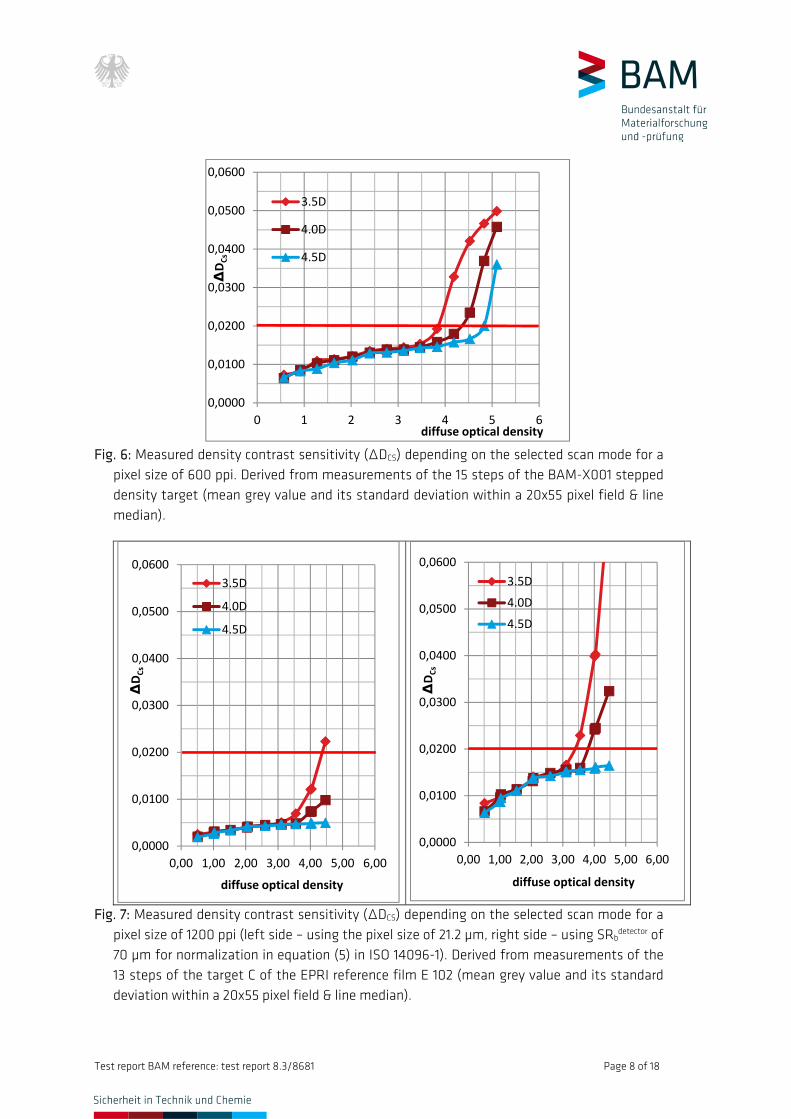
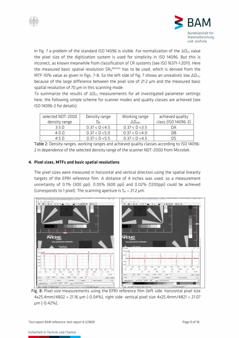
3. Density Contrast Sensitivities (ΔDCS) After verification of the linear CTC curve of the scanner NDT-2000 the ΔDCS can be calculated according to equation (5) in ISO 14096-1 from the measured standard deviations in the raw data of the 15 fields of the BAM film step density target. Fig. 5-7 show the resulting ΔDCS curves in dependence of the scanning modes and the selected pixel sizes. The horizontal red line at ΔDCS =0.02 in figs 5-7 is the maximum acceptable digitization noise (1% at D=2, 0.5% at D=4) for lossless digitization according to ISO 14096.
Fig. 5: Measured density contrast sensitivity (ΔDCS) depending on the selected scan mode for a
pixel size of 300 ppi. Derived from measurements of the 15 steps of the BAM-X001 stepped density target (mean grey value and its standard deviation within a 20x55 pixel field & line median).
0,0000
0,0100
0,0200
0,0300
0,0400
0,0500
0,0600
0 1 2 3 4 5 6
∆DCs
diffuse optical density
3.5D
4.0D
4.5D
Test report BAM reference: test report 8.3/8681 Page 8 of 18
Fig. 6: Measured density contrast sensitivity (ΔDCS) depending on the selected scan mode for a
pixel size of 600 ppi. Derived from measurements of the 15 steps of the BAM-X001 stepped density target (mean grey value and its standard deviation within a 20x55 pixel field & line median).
Fig. 7: Measured density contrast sensitivity (ΔDCS) depending on the selected scan mode for a
pixel size of 1200 ppi (left side – using the pixel size of 21.2 μm, right side – using SRbdetector of
70 μm for normalization in equation (5) in ISO 14096-1). Derived from measurements of the 13 steps of the target C of the EPRI reference film E 102 (mean grey value and its standard deviation within a 20x55 pixel field & line median).
0,0000
0,0100
0,0200
0,0300
0,0400
0,0500
0,0600
0 1 2 3 4 5 6
∆DCs
diffuse optical density
3.5D
4.0D
4.5D
0,0000
0,0100
0,0200
0,0300
0,0400
0,0500
0,0600
0,00 1,00 2,00 3,00 4,00 5,00 6,00
∆DCs
diffuse optical density
3.5D
4.0D
4.5D
0,0000
0,0100
0,0200
0,0300
0,0400
0,0500
0,0600
0,00 1,00 2,00 3,00 4,00 5,00 6,00
∆DCs
diffuse optical density
3.5D
4.0D
4.5D
Test report BAM reference: test report 8.3/8681 Page 9 of 18
In fig. 7 a problem of the standard ISO 14096 is visible. For normalization of the ΔDCS value the pixel size of the digitization system is used for simplicity in ISO 14096. But this is incorrect, as known meanwhile from classification of CR systems (see ISO 16371-1:2011). Here the measured basic spatial resolution SRb
detector has to be used, which is derived from the MTF-10% value as given in figs. 7-8. So the left side of fig. 7 shows an unrealistic low ΔDCS, because of the large difference between the pixel size of 21.2 μm and the measured basic spatial resolution of 70 μm in this scanning mode. To summarize the results of ΔDCS measurements for all investigated parameter settings here, the following simple scheme for scanner modes and quality classes are achieved (see ISO 14096-2 for details):
selected NDT-2000 density range
Density range DR
Working range ΔDWR
achieved quality class (ISO 14096-2)
3.5 D 0.37 < D <4.5 0.37 < D <3.5 DA 4.0 D 0.37 < D <5.0 0.37 < D <4.0 DB 4.5 D 0.37 < D <5.5 0.37 < D <4.5 DS
Table 2: Density ranges, working ranges and achieved quality classes according to ISO 14096-2 in dependence of the selected density range of the scanner NDT-2000 from Microtek.
4. Pixel sizes, MTFs and basic spatial resolutions
The pixel sizes were measured in horizontal and vertical direction using the spatial linearity targets of the EPRI reference film. A distance of 4 inches was used, so a measurement uncertainty of 0.1% (300 ppi). 0.05% (600 ppi) and 0.02% (1200ppi) could be achieved (corresponds to 1 pixel). The scanning aperture is SA = 21.2 μm.
Fig. 8: Pixel size measurements using the EPRI reference film (left side: horizontal pixel size
4x25.4mm/4802 = 21.16 μm (-0.04%), right side: vertical pixel size 4x25.4mm/4821 = 21.07 μm (-0.42%).

Test report BAM reference: test report 8.3/8681 Page 10 of 18
This result is typically for a line scanning system: The pixel size within the line is exactly adjusted during the adjustment of the system sharpness after manufacturing, but the pixel size in vertical direction deviates more caused by mechanical tolerances during film movement. The measured values of the actual pixel sizes of all scanning modes are given in Table 3, the deviations found are far below 1% and therefore fully acceptable.
selected pixel den-sity & orientation
nominal size [μm]
measured size [μm]
deviation [%] and pixel
measurement uncertainty
300 ppi horizontal 84.67 84.67 0%, 0 pixel 0.1%, 1 pixel 300 ppi vertical 84.67 84.53 -0,17%, +2 pixel 0.1%, 1 pixel 600 ppi horizontal 42.33 42.33 0%, 0 pixel 0.05%, 1 pixel 600 ppi vertical 42.33 42.23 -0.25%, +6 pixel 0.05%, 1 pixel 1200 ppi horizontal 21.17 21.16 -0.04%, +2 pixel 0.02%, 1 pixel 1200 ppi vertical 21.17 21.07 -0.42%, +21 pixel 0.02%, 1 pixel
Table 3: Measured pixel sizes P and deviations from the nominal values
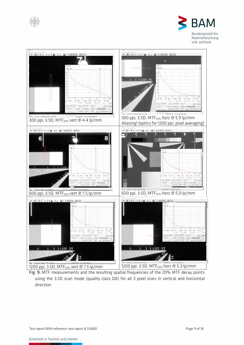
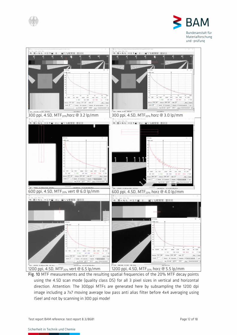
The following MTF curves were measured using the EPRI reference film according to ISO 14096-1 and ASTM E 1936 in the different scan modes (only 6 of 9 tested scanning modes are show here) using the edges of target H (optical density change from 0.5 to 3.0) of the EPRI reference film. As ISO 14096-1 requires a calculation of the modulation transfer curve (MTF) using a sharp edge (the outer edge of target H of the EPRI reference film) at the density axis, which is directly proportional to the raw grey values of the scanner NDT-2000. This is a special requirement of ISO 14096, because the optical density of the film is proportional to the detected radiation dose of the X-rays. This requirement of ISO 14096 is for direct comparison of the digitized film images to other industrial radiation imaging detectors like imaging plates in CR or digital detector arrays. They all provide grey values proportional to the radiation dose. The consequences for MTF measurements is discussed shortly in chapter 5. Originally, the MTF is defined for a linear optical system characterization, so it should be calculated on an axis of light intensity penetrating the film and not on the optical density axis of the scanned film.
Test report BAM reference: test report 8.3/8681 Page 11 of 18
300 ppi, 3.5D, MTF20% vert @ 4.4 lp/mm
300 ppi, 3.5D, MTF20% horz @ 5.9 lp/mm Aliasing! (optics for 1200 ppi, pixel averaging)
600 ppi, 3.5D, MTF20% vert @ 7.5 lp/mm
600 ppi, 3.5D, MTF20% horz @ 5.0 lp/mm
1200 ppi, 3.5D, MTF20% vert @ 7.5 lp/mm 1200 ppi, 3.5D, MTF20% horz @ 5.3 lp/mm Fig. 9: MTF measurements and the resulting spatial frequencies of the 20% MTF decay points
using the 3.5D scan mode (quality class DA) for all 3 pixel sizes in vertical and horizontal direction.
Test report BAM reference: test report 8.3/8681 Page 12 of 18
300 ppi, 4.5D, MTF20%horz @ 3.2 lp/mm
300 ppi, 4.5D, MTF20% horz @ 3.0 lp/mm
600 ppi, 4.5D, MTF20% vert @ 6.0 lp/mm
600 ppi, 4.5D, MTF20% horz @ 4.0 lp/mm
1200 ppi, 4.5D, MTF20% vert @ 6.5 lp/mm 1200 ppi, 4.5D, MTF20% horz @ 5.5 lp/mm Fig. 10 MTF measurements and the resulting spatial frequencies of the 20% MTF decay points
using the 4.5D scan mode (quality class DS) for all 3 pixel sizes in vertical and horizontal direction. Attention: The 300ppi MTFs are generated here by subsampling the 1200 dpi image including a 7x7 moving average low pass anti alias filter before 4x4 averaging using ISee! and not by scanning in 300 ppi mode!
Test report BAM reference: test report 8.3/8681 Page 13 of 18
Table 4 summarises all MTF measurements and provides additionally the spatial frequencies MTF10% of the 10% MTF values, which is used to calculate the basic spatial detector resolution SRb
detector of the system as SRbdetector = 1/(2*MTF10%) (see ASTM E 2445-16 for more
details):
Scan mode – pixel size & density range
MTF20% - spatial frequency [lp/mm]
MTF10% - spatial frequency [lp/mm]
SRbdetector
- basic spatial resolution
[μm] 1200 ppi, 4.5D, horizontal 5.5 7.0 70 1200 ppi, 4.5D, vertical 6.5 10 50 1200 ppi, 3.5D, horizontal 5.3 7.0 70 1200 ppi, 3.5D, vertical 7.5 12 42 600 ppi, 4.5D, horizontal 4.0 6.0 85 600 ppi, 4.5D, vertical 6.0 9.0 55 600 ppi, 3.5D, horizontal 5.0 7.0 70 600 ppi, 3.5D, vertical 7.5 9.0 55 300 ppi, 4.5D, horizontal 5.9 6.4 80 300 ppi, 4.5D, vertical 4.4 5.5 90 300 ppi, subsampled, horizontal 3.0 4.0 125 300 ppi, subsampled, vertical 3.2 4.2 120
Table 4: Summary of the MTF measurements as shown in fig. 9 & 10 in dependence of scan mode (pixel size and density range). The given basic spatial detector resolution is calculated from the MTF10% values.
It is typically for line scanners that the MTF values within the scanline are lower than the MTF values in direction of the movement. This is caused by the additionally scattered light (flare) within the line detector, which is reduced between neighboured lines. The differences between the 1200 ppi and the 600 ppi modes are insignificant, which means, that the image sharpness is already limited for a pixel size of 42.3 μm and the higher pixel resolution of 21.2 μm does not add any increase in image sharpness. This is also confirmed by the best achieved basic spatial resolution of 70 μm according to table 4, which should be a good reason for optical improvements of a scanner with 21.2 μm pixel size.
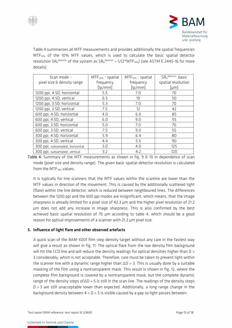
5. Influence of light flare and other observed artefacts
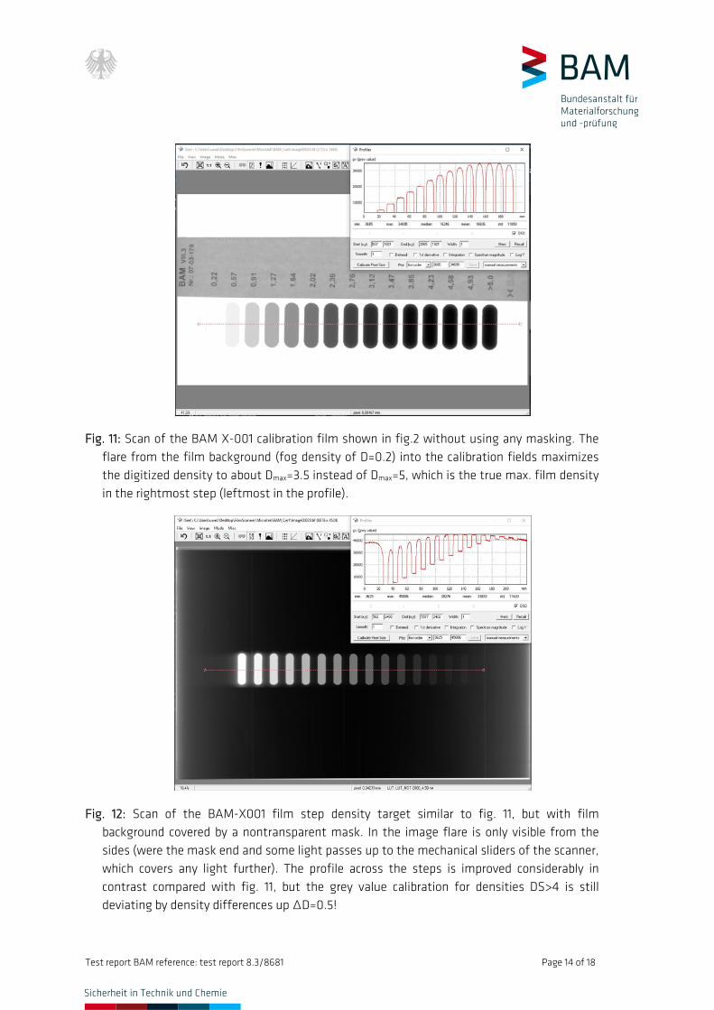
A quick scan of the BAM-X001 film step density target without any care in the fastest way will give a result as shown in fig. 11. The optical flare from the low density film background will hit the CCD line and will reduce the density readings for optical densities higher than D > 3 considerably, which is not acceptable. Therefore, care must be taken to prevent light within the scanner line with a dynamic range higher than ΔD > 3. This is usually done by a suitable masking of the film using a nontransparent mask. This result is shown in fig. 12, where the complete film background is covered by a nontransparent mask, but the complete dynamic range of the density steps ofΔD ≈ 5 is still in the scan line. The readings of the density steps D > 3 are still unacceptable lower than expected. Additionally, a long range change in the background density between 4 < D < 5 is visible caused by a gap so light passes between
Test report BAM reference: test report 8.3/8681 Page 14 of 18
Fig. 11: Scan of the BAM X-001 calibration film shown in fig.2 without using any masking. The flare from the film background (fog density of D=0.2) into the calibration fields maximizes the digitized density to about Dmax=3.5 instead of Dmax=5, which is the true max. film density in the rightmost step (leftmost in the profile).
Fig. 12: Scan of the BAM-X001 film step density target similar to fig. 11, but with film background covered by a nontransparent mask. In the image flare is only visible from the sides (were the mask end and some light passes up to the mechanical sliders of the scanner, which covers any light further). The profile across the steps is improved considerably in contrast compared with fig. 11, but the grey value calibration for densities DS>4 is still deviating by density differences up ΔD=0.5!

Test report BAM reference: test report 8.3/8681 Page 15 of 18
the film mask rims and the mechanical scanner sliders, which limits the film illumination width. So this set-up is still not optimal for correct density readings of this film target, deviations up to ΔD=0.5 are still observed for densities higher than D>4. This shows the sensitivity of this scanning system against flare within the scan line.
Only the scan orientation of the BAM-X001 film step density target as shown in fig. 3 (film covered by mask and per scan line only 1 density step) will prevent flare from reaching the scan line and allows determining the correct scanner calibration over the full dynamic range up to D≈5 as shown in fig. 4 for measurement of the CTC. Here the absolute deviations of the density readings of all density steps are smaller than ΔD=0.05, which is sufficient.
Another problem in measuring the MTF response of the scanner is the intensity axis, which is proportional the optical density of the film. In theory, the MTF of a digitization system is defined as a linear system characteristic, i.e. proportional to the detected light intensity which is transmitted through the film. ISO 14096-1 defines an MTF proportional to the optical density of the film, which is a logarithmic measure of the transmitted light intensity. The result of this difference in MTF calculation is shown in fig. 14.
Fig.14: MTF calculation with identical set-up as in fig. 10 lower row and shown again b), additionally the edge profile in d) and after delogarithmization the linear MTF response in a) and the used profile in c). The MTF calculation using the optical density axis introduces a
Test report BAM reference: test report 8.3/8681 Page 16 of 18
strong low frequency drop and reduces the MTF20% value from 8.9 lp/mm (linear axis) to 5.4 lp/mm (density axis).
The calculation of the MTF using a density proportional grey value generated a low frequency drop caused by the logarithm of the light intensity to obtain the optical density values. This reduced for the NDT-2000 scanner the measured MTF20% value from 8.9 to 5.4 lp/mm. The basic spatial resolution (based on the MTF10% value) is increased from 45 μm to 70 μm.
This definition to calculate the MTF on a logarithmic grey scale axis proportional to the film density was selected with intention during development of ISO 14096, to make film digitization systems comparable with imaging plates (CR) or DDAs. All have grey scale responses which are proportional to the detected radiation dose. Therefore, this MTF degeneration of this film digitization system has to be taken into account.
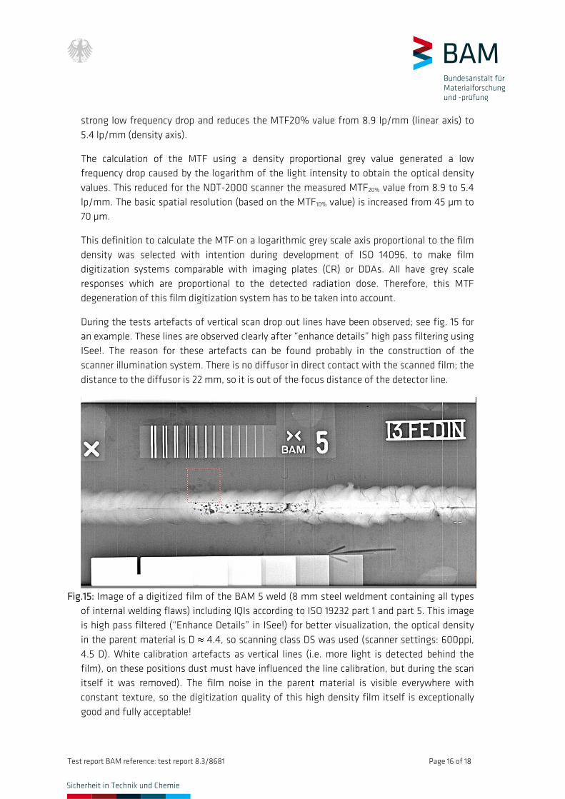
During the tests artefacts of vertical scan drop out lines have been observed; see fig. 15 for an example. These lines are observed clearly after “enhance details” high pass filtering using ISee!. The reason for these artefacts can be found probably in the construction of the scanner illumination system. There is no diffusor in direct contact with the scanned film; the distance to the diffusor is 22 mm, so it is out of the focus distance of the detector line.
Fig.15: Image of a digitized film of the BAM 5 weld (8 mm steel weldment containing all types
of internal welding flaws) including IQIs according to ISO 19232 part 1 and part 5. This image is high pass filtered (“Enhance Details” in ISee!) for better visualization, the optical density in the parent material is D 4.4, so scanning class DS was used (scanner settings: 600ppi, 4.5 D). White calibration artefacts as vertical lines (i.e. more light is detected behind the film), on these positions dust must have influenced the line calibration, but during the scan itself it was removed). The film noise in the parent material is visible everywhere with constant texture, so the digitization quality of this high density film itself is exceptionally good and fully acceptable!

Test report BAM reference: test report 8.3/8681 Page 17 of 18
A diffusor for illumination of the film in direct contact to it would prevent that dust will influence the scanner calibration without film before the film scanning is started. Normally dust in scanner or on the film will create short dark spots, but here we have the opposite. This means the dust is imaged sharply during the calibration procedure and influences only a few pixels, which afterwards is stored in the calibration table. During the scan this dust particles are removed and this results in white lines, because these pixels have wrong gain calibration values for the complete scan. Using a diffusor in direct contact with the film would help in this situation, because of the diffuse light small dust particles should not be imaged sharply and should not influence the calibration process. At least we have never before seen such problems with other scanners and manufacturers.
6. Achieved digitization quality classes and summary
To conclude the following scanner characteristics were found for the digitization system “NDT-2000” from Microtek:
1. The highest digitization quality class ”DS 5.5” is reached for 1200 ppi (21.2 μm pixel size) using the density range “4.5 D”. The maximum spatial resolution is 5.5 lp/mm. Lower digitization quality classes can be achieved according to table 2 using faster scanner modes.
2. The characteristic transfer curve (CTC) of this system is calibrated by the manufacturer and follows the simple relationship Gv = 10000*D. The measured deviations are below D≤0.05 in all scanning modes, when optical flare is prevented to reach the scanner line. Any optical flare will modify the local CTC with differences up to ΔD ≈ -1 for densities D > 4. The working range DWR is 0.37 < D < 4.5 optical densities, the minimum optical density digitized is Dmin = 0.37, the maximum optical density digitized is Dmax = 5.5. The density sampling pitch ΔDSP = 0.0001 is constant over this density range This is more than ISO 14096 requires and corresponds to the complete dynamic range in NDT.
3. The maximum basic spatial detector resolution of this digitization system is SRb
detector = 70 μm for the 1200 ppi scanning mode. 4. A very usefully, practically and easily adjustable masking system is built into the
illumination bar of the scanner, which prevents any flare outside the film borders to reach the scanning line. This is an essential feature to guarantee a correct CTC during digitization with the smallest flare contributions as possible.
5. Vertical scan drop out lines were detected resulting from calibration of dust particles. This can be reduced by carefully cleaning of the 2 glasses in contact with the scanned film. The manufacturer provides guidelines for best cleaning.
6. No further artefacts of any insufficient scanner correction could be found, i.e. offset subtraction, stability and linearity deviations of the CTC is smaller than the observed scanner noise level.
Test report BAM reference: test report 8.3/8681 Page 18 of 18
Uncertainties
The uncertainties associated with the measured parameters are given as expanded uncertainties based on 2x the standard deviation of several single measurements. The BAM policy on statement of uncertainties follows reference [3]. The uncertainties for the MTF measurements are 0.5 lp/mm, for the pixel size measurements 1 pixel, for the ΔDCS measurement 5% and for the CTC fits ΔD = 0.05. But the latter small uncertainty may be superimposed by a much larger systematic reduction in densities by optical flare down to lower optical densities up to ΔD = -1 for D > 4. This systematic error should be reduced as much as possible by suitable masking to minimize flare effects.
References
[1] BAM reference procedure RRR 17 “Determination of image quality parameters of digital image detectors for industrial radiology”, see https://rrr.bam.de/RRR/Content/EN/Downloads/Reference-Procedures/17_determination-image-quality.html
[2] ASTM E 1936 reference film for NDT scanner tests, available as RR E 1936 adjunct from ASTM
[3] ISO/IEC Guide 98-3:2008, “Uncertainty of measurement -- Part 3: Guide to the expression of uncertainty in measurement (GUM: 1995)”, ISO, Geneva, Switzerland (2008)
Federal Institute for Materials Research and Testing (BAM) Bundesanstalt für Materialforschung und –prüfung (BAM)
Unter den Eichen 87 12200 Berlin
Division 8.3 “Radiological Methods”
on behalf
on behalf
Dr. rer. nat. Anja Waske Head of Division 8.3
Dr. rer. nat. Uwe Zscherpel Officer in charge of the test
Distribution list: 1st copy: Customer 2nd copy: BAM 8.3
BAM Department 8 is a testing laboratory accredited by Deutsche Akkreditierungsstelle GmbH (DAkkS) against ISO/IEC 17025.
The accreditation is valid for the testing procedures listed in the certificate D-PL-11075-08-00.