characterization of collective ground states in single layer nbse · 2015-11-06 ·...
TRANSCRIPT
1
This document is the unedited Author’s version of a Submitted Work that was subsequently accepted
for publication in Nature Physics. To access the final edited and published work see
http://www.nature.com/nphys/journal/vaop/ncurrent/full/nphys3527.html
Characterization of collective ground states in single-layer NbSe2
Miguel M. Ugeda*1,2,3, Aaron J. Bradley1, Yi Zhang4,5,6, Seita Onishi1, Yi Chen1, Wei
Ruan1,7, Claudia Ojeda-Aristizabal1,8,9, Hyejin Ryu4, Mark T. Edmonds1,10, Hsin-Zon
Tsai1, Alexander Riss1,11, Sung-Kwan Mo4, Dunghai Lee1, Alex Zettl1,8,12, Zahid Hussain4,
Zhi-Xun Shen5,13 and Michael F. Crommie*1,8,12 1Department of Physics, University of California at Berkeley, Berkeley, California 94720, USA.
2CIC nanoGUNE, 20018 Donostia-San Sebastian, Spain.
3Ikerbasque, Basque Foundation for Science, 48011 Bilbao, Spain.
4Advanced Light Source, Lawrence Berkeley National Laboratory, Berkeley, California 94720, USA.
5Stanford Institute for Materials and Energy Sciences, SLAC National Accelerator Laboratory, Menlo
Park, California 94025, USA.
6National Laboratory of Solid State Microstructures, School of Physics, Collaborative Innovation
Center of Advanced Microstructures, Nanjing University, Nanjing 210093, China.
7State Key Laboratory of Low Dimensional Quantum Physics, Department of Physics, Tsinghua
University, Beijing 100084, China.
8Materials Sciences Division, Lawrence Berkeley National Laboratory, Berkeley, California 94720,
USA.
9Department of Physics & Astronomy, California State University Long Beach, Long Beach,
California 90840, USA.
10School of Physics and Astronomy, Monash University, Clayton,Victoria 3800, Australia.
11Institute of Applied Physics, Vienna University of Technology, 1040Wien, Austria.
12Kavli Energy NanoSciences Institute at the University of California Berkeley and the Lawrence
Berkeley National Laboratory, Berkeley, California 94720, USA.
13Geballe Laboratory for Advanced Materials, Departments of Physics and Applied Physics, Stanford
University, Stanford, California 94305, USA.
* Corresponding authors: [email protected] and [email protected]
2
Abstract
Layered transition metal dichalcogenides (TMDs) are ideal systems for exploring the effects of
dimensionality on correlated electronic phases such as charge density wave (CDW) order and
superconductivity. In bulk NbSe2 a CDW sets in at TCDW = 33 K and superconductivity sets in at Tc =
7.2 K. Below Tc these electronic states coexist but their microscopic formation mechanisms remain
controversial. Here we present an electronic characterization study of a single 2D layer of NbSe2 by
means of low temperature scanning tunneling microscopy/spectroscopy (STM/STS), angle-resolved
photoemission spectroscopy (ARPES), and electrical transport measurements. We demonstrate that
3x3 CDW order in NbSe2 remains intact in 2D. Superconductivity also still remains in the 2D limit,
but its onset temperature is depressed to 1.9 K. Our STS measurements at 5 K reveal a CDW gap of
= 4 meV at the Fermi energy, which is accessible via STS due to the removal of bands crossing the
Fermi level for a single layer. Our observations are consistent with the simplified (compared to bulk)
electronic structure of single-layer NbSe2, thus providing new insight into CDW formation and
superconductivity in this model strongly-correlated system.
3
Many-body electronic ground states can be quite sensitive to the spatial dimensions of a
material1, 2, 3, 4. In transition metal dichalcogenide materials, for example, significant differences are
expected in charge density wave and superconducting (SC) phases as dimensionality is reduced from a
bulk 3D material to a single-layer 2D material5, 6, 7. NbSe2 is a model system in this regard, as it has
been predicted to preserve its CDW order in the single-layer limit, although with significantly
shortened CDW wavevector (qCDW)5. A metal to semi-metal transition has also been predicted for
NbSe2 when it is reduced to the 2D limit 5, 6, 8. Previous work has shown that the superconducting
transition temperature for NbSe2 decreases from its bulk value of TC = 7.2 K as the thickness is
reduced9, 10, 11, but no experimental studies have yet been performed that explore the interplay between
NbSe2 superconductivity and CDW formation in the extreme 2D limit.
CDW behavior in the 3D limit of NbSe2, on the other hand, has been well studied, although the
origin of the bulk CDW transition at TCDW = 33K remains controversial. Recent experiments suggest
that electron-phonon coupling plays a dominant role in triggering the CDW phase12, 13, 14, 15, 16, 17, 18,
thus casting doubt on mechanisms involving Fermi-surface nesting19, 20, 21, 22 and saddle-point
singularities23, 24. Critical experimental parameters associated with the CDW, namely the magnitude
and location of the energy gap also remain unclear. Previous STS measurements on bulk NbSe2 in the
CDW phase have revealed an unexpectedly large gap-like structure having width 2 70 meV25, 26. In
contrast, low-temperature ARPES measurements performed on bulk NbSe2 show an anisotropic CDW
energy gap at EF with a width of only a few meV15. In general, it is expected that a weak-coupling
CDW derived from Fermi surface nesting should open a small gap on the Fermi surface, while a strong
coupling CDW caused by electron-phonon coupling should open a larger gap away from the Fermi
surface.
4
Here we report new measurements on the electronic structure of single-layer NbSe2 using a
combination of STM/STS, ARPES, and electronic transport techniques. This allows us to directly
probe the electronic ground state of NbSe2 in the 2D limit, enabling interrogation of the effects of
dimensionality and interlayer coupling in this layered material. We observe a reduction in the number
of Fermi-level-crossing bands from three (for bulk) to one in the single-layer limit. Despite this change
in electronic structure, CDW order in single-layer NbSe2 remains unchanged compared to the bulk
case. The simplified bandstructure of single-layer NbSe2, however, allows unprecedented access to the
NbSe2 CDW energy gap via STS (observed here to be 2 = 8 meV centered at EF). Superconductivity
in NbSe2, on the other hand, is significantly suppressed in the 2D limit, showing an onset of
superconducting fluctuations at 1.9 K and a broadened superconducting transition with a midpoint at
0.65 K consistent with a Kosterlitz-Thouless transition. The one Nb antibonding band5 that remains in
the Fermi surface of single-layer NbSe2 thus appears to play a critical role in the NbSe2 CDW state,
while the absent bands have a stronger influence on NbSe2 superconductivity15. These results provide a
new window into the electronic structure of single-layer NbSe2 and help to clarify the longstanding
debate over NbSe2 CDW formation.
Our experiments were carried out on high-quality submonolayer NbSe2 films grown on
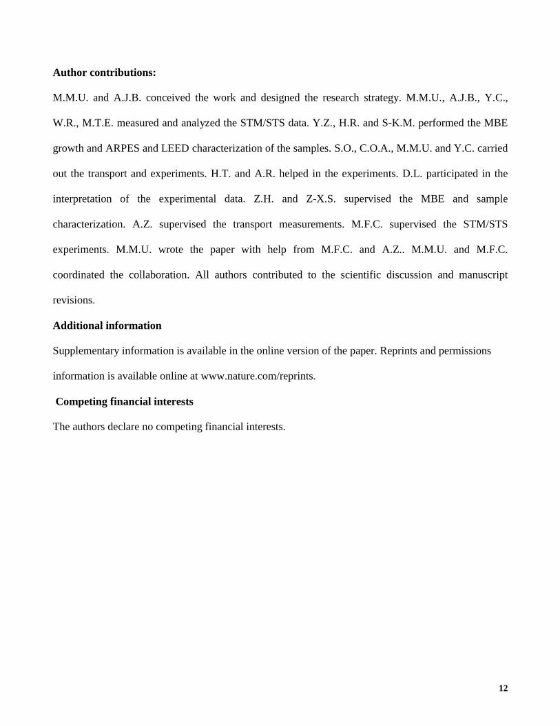
epitaxial bilayer graphene (BLG) on 6H-SiC(0001), as sketched in Fig. 1a. The large-scale STM image
in Fig. 1b shows the typical morphology of our single-layer NbSe2 samples. Black regions correspond
to the BLG substrate while the NbSe2 layer is purple. The temperature dependence of the electronic
ground state of single-layer NbSe2 was measured via STM and electrical transport. Fig. 1c-e show
STM topographic data for selected temperatures from T = 45 K to T = 5 K. At T = 45 K, well above
the critical transition temperature for bulk NbSe2 (TCDW = 33 K), only the undistorted crystal structure
is observed (Fig. 1c). At a lower temperature of T = 25 K, weak and spotty signatures of a superlattice

5
are apparent (Fig. 1d). Here small CDW patches surrounded by non CDW regions can be seen. This is
reminiscent of STM images of bulk NbSe2 at temperatures close to the CDW transition temperature.17
At T = 5 K, the 3 x 3 CDW superlattice is fully and uniformly developed for single-layer NbSe2 (Fig.
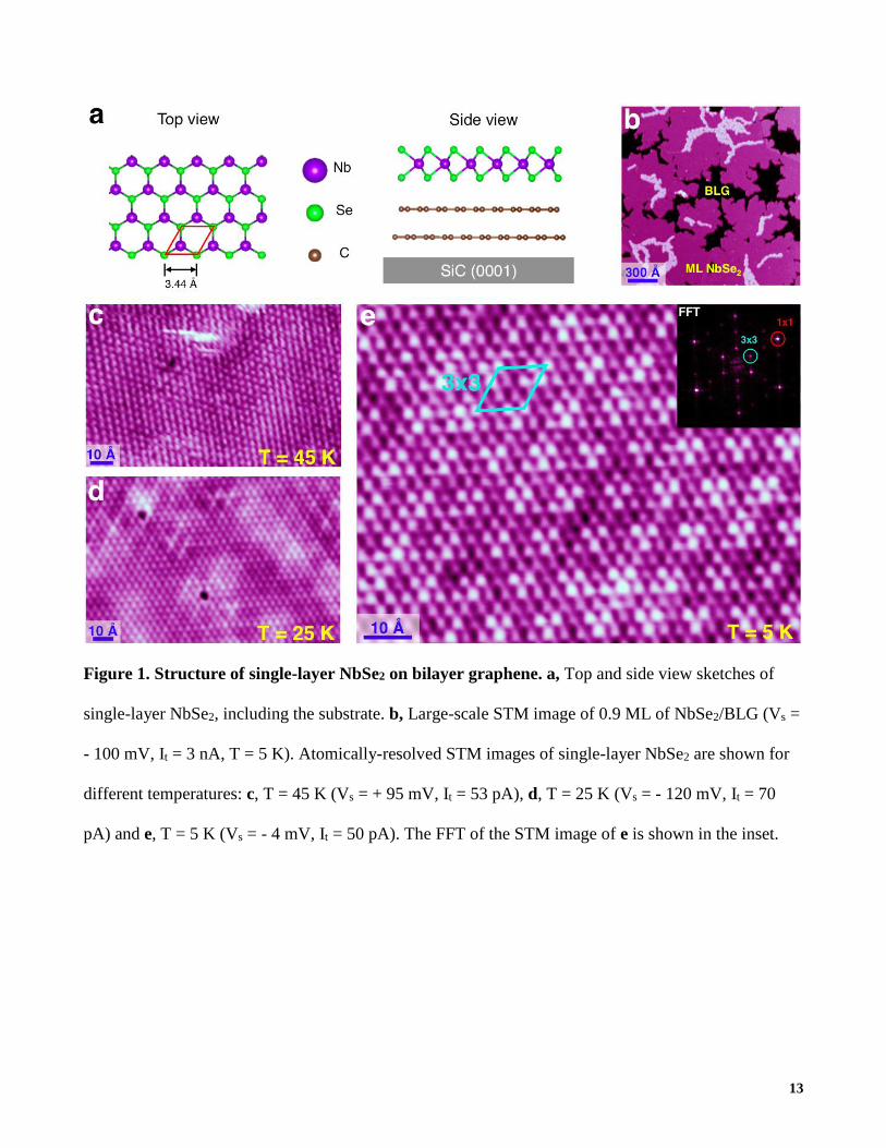
1e). Fig. 2 shows the temperature-dependent electrical resistance of single-layer NbSe2 on BLG,
acquired using a 4-probe low-excitation dc method (see SI). A downturn in the resistance begins at T
= 1.9 K, indicative of the onset of superconducting fluctuations, while the superconducting transition
midpoint is at 0.65 K and the zero resistance point at 0.46 K, as shown inset. This data indicate that the
trend of reduced superconducting transition (Tc) with decreasing layer number in NbSe211, 12 continues
down to the single layer limit.
Fig. 1e shows that the 3 x 3 CDW superlattice is aligned with the 1 x 1 atomic arrangement for
single-layer NbSe2, similar to what has been seen previously in STM images of bulk NbSe216, 17, 27. The
3 x 3 superlattice remains unchanged in our STM images regardless of the orientation between the
NbSe2 layer and the BLG (see STM and LEED data in the SI). This rules out the possibility that the 3 x
3 superlattice observed here in single-layer NbSe2 is a moiré pattern (moiré patterns have been
observed in MoSe2/BLG28). A 3 x 3 moiré pattern formation requires a quasi-commensurate match
between overlayer and substrate atomic lattices, which does not occur here since NbSe2 has a much
larger unit cell than graphene. The rotational disorder we find in single-layer NbSe2 with respect to the
BLG substrate indicates weak coupling between them (similar weak coupling has been demonstrated
for epitaxial graphene grown on different metal substrates29).
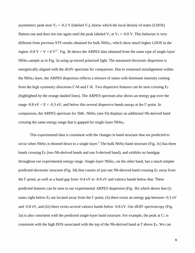
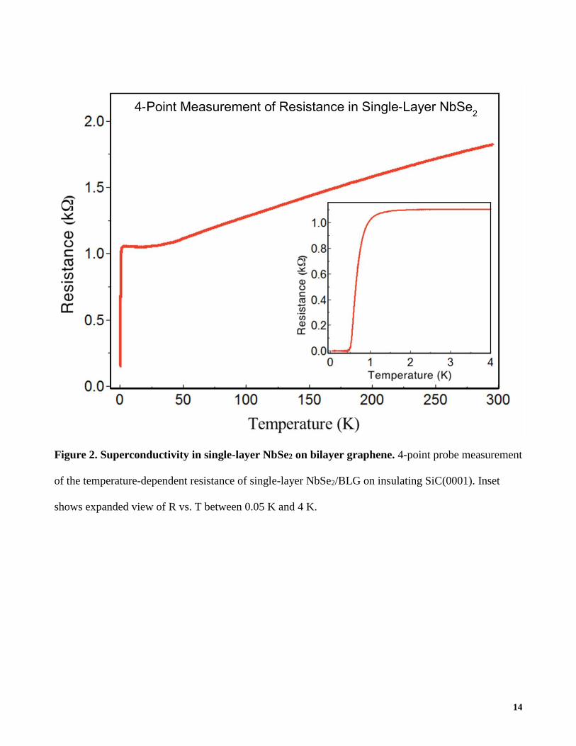
We experimentally determined the electronic structure of single-layer NbSe2 through a
combination of STS and ARPES. Fig. 3a shows a typical STM dI/dV spectrum of single-layer NbSe2
taken over a large bias range. In the positive bias (empty state) region the most pronounced feature is
the peak labeled C1 at Vs = 0 .5 V. For negative bias (filled states) we observe a very shallow
6
asymmetric peak near Vs = -0.2 V (labeled V1), below which the local density of states (LDOS)
flattens out and does not rise again until the peak labeled V2 at Vs = -0.8 V. This behavior is very
different from previous STS results obtained for bulk NbSe2, which show much higher LDOS in the
region -0.8 V < V < 0 V17. Fig. 3b shows the ARPES data obtained from the same type of single-layer
NbSe2 sample as in Fig. 3a using sp-mixed polarized light. The measured electronic dispersion is
energetically aligned with the dI/dV spectrum for comparison. Due to rotational misalignment within
the NbSe2 layer, the ARPES dispersion reflects a mixture of states with dominant intensity coming
from the high symmetry directions Γ-M and Γ-K. Two dispersive features can be seen crossing EF
(highlighted by the orange dashed lines). The ARPES spectrum also shows an energy gap over the
range -0.8 eV < E < -0.3 eV, and below this several dispersive bands merge at the Γ-point. In
comparison, the ARPES spectrum for 5ML–NbSe2 (see SI) displays an additional Nb-derived band
crossing the same energy range that is gapped for single-layer NbSe2.
This experimental data is consistent with the changes in band structure that are predicted to
occur when NbSe2 is thinned down to a single layer.5 The bulk NbSe2 band structure (Fig. 3c) has three
bands crossing EF (two Nb-derived bands and one S-derived band), and exhibits no bandgap
throughout our experimental energy range. Single-layer NbSe2, on the other hand, has a much simpler
predicted electronic structure (Fig. 3d) that consist of just one Nb-derived band crossing EF away from
the -point, as well as a band gap from -0.4 eV to -0.8 eV and valence bands below that. These
predicted features can be seen in our experimental ARPES dispersion (Fig. 3b) which shows that (i)
states right below EF are located away from the-point, (ii) there exists an energy gap between -0.3 eV
and -0.8 eV, and (iii) there exists several valence bands below -0.8 eV. Our dI/dV spectroscopy (Fig.
3a) is also consistent with the predicted single-layer band structure. For example, the peak at C1 is
consistent with the high DOS associated with the top of the Nb-derived band at Γ above EF. We can
7
also associate the shallow peak at V1 with the Nb band right below EF. The flat dI/dV region seen
between V1 and V2 is consistent with the predicted bandgap (the fact that the dI/dV does not reach zero
is due to residual tunneling into the BLG substrate), and the peaks at V2 and V3 are consistent with the
lower-energy valence bandstructure5, 30. Overall, these features are very different from previous STS
spectra obtained for bulk NbSe2, which show much higher LDOS below EF and no signs of a bandgap
in the filled-state regions17. This is due to the additional electronic bands and resulting DOS expected
in this energy range for bulk NbSe2 as compared to single-layer NbSe2 (Figs. 3c-d). This is also
reflected in the additional band that can be seen in the ARPES spectrum of 5ML–NbSe2 (SI), which
corresponds to a Nb bonding band (the blue band in Figs. 3c-d). The Se-derived band (green band in
Figs. 3c-d) is typically not observed in ARPES due to the high kz dispersion.
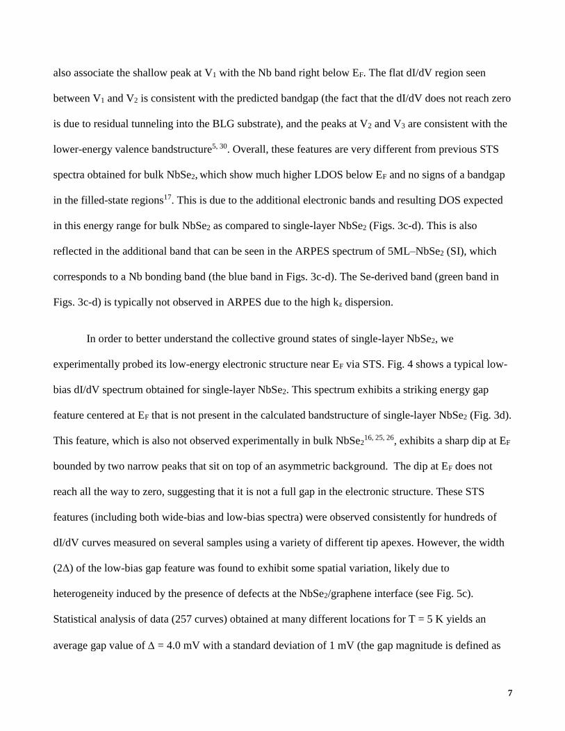
In order to better understand the collective ground states of single-layer NbSe2, we
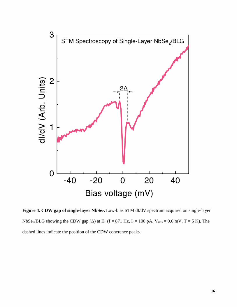
experimentally probed its low-energy electronic structure near EF via STS. Fig. 4 shows a typical low-
bias dI/dV spectrum obtained for single-layer NbSe2. This spectrum exhibits a striking energy gap
feature centered at EF that is not present in the calculated bandstructure of single-layer NbSe2 (Fig. 3d).
This feature, which is also not observed experimentally in bulk NbSe216, 25, 26, exhibits a sharp dip at EF
bounded by two narrow peaks that sit on top of an asymmetric background. The dip at EF does not
reach all the way to zero, suggesting that it is not a full gap in the electronic structure. These STS
features (including both wide-bias and low-bias spectra) were observed consistently for hundreds of
dI/dV curves measured on several samples using a variety of different tip apexes. However, the width
(2Δ) of the low-bias gap feature was found to exhibit some spatial variation, likely due to
heterogeneity induced by the presence of defects at the NbSe2/graphene interface (see Fig. 5c).
Statistical analysis of data (257 curves) obtained at many different locations for T = 5 K yields an
average gap value of = 4.0 mV with a standard deviation of 1 mV (the gap magnitude is defined as

8
half the energy distance between the two peaks bracketing the gap). This value is in agreement with
anisotropic gap-opening observed previously by low-temperature ARPES15 at the Fermi surface near
the K point in the band that is predicted to remain in the 2D single-layer limit of NbSe2 (orange band in
Fig. 3d).
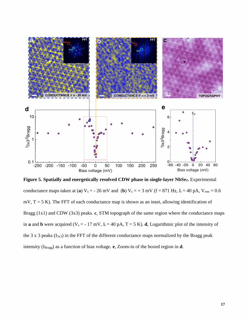
In order to better understand the origin of the EF gap feature of Fig. 4, we performed spatially-
resolved dI/dV mapping of single-layer NbSe2 at different bias voltages near EF. Figs. 5a and 5b show
dI/dV conductance maps of the same region taken at bias voltages outside (Vb = -26 mV) and inside
(Vb = 3 mV) the low-bias gap region (Fig. 5c shows STM topography for this same region). The dI/dV
conductance map taken at an energy outside of the gap (Fig. 5a) clearly shows the 3 x 3 CDW pattern,
but the conductance map measured at an energy inside of the gap (Fig. 5b) shows no sign of the CDW.
We Fourier analyzed dI/dV maps taken at different voltages in order to obtain a more quantitative
understanding of the energy dependence of CDW electronic features. Fig. 5d shows the relative
intensity of the resulting 3 x 3 peaks (I3x3) in the FFTs normalized to the intensity of the 1 x 1 Bragg
peaks (IBragg). This ratio (I3x3/IBragg(E)) is a measure of the strength of the CDW modulation on the
density of states. As seen in Fig. 5d, I3x3/IBragg has large amplitude at energies far from EF, but shows a
decrease of nearly two orders of magnitude very close to EF. Fig. 5e shows a higher-resolution plot of
the dip in I3x3/IBragg at EF (boxed region in Fig. 5d). The decrease in the ratio I3x3/IBragg is seen to follow
the energy dependence of the low-bias gap-feature observed in dI/dV spectroscopy. This correlation of
CDW intensity with gap energy dependence suggests that the gap is the result of CDW order. In
particular, the diminishing CDW intensity for in-gap energies suggests that the residual LDOS within
the gap arises from a portion of the Fermi surface that is not gapped by CDW order.
Our results allow us to draw some conclusions regarding different models of CDW formation
in NbSe2. First, we rule out recently proposed dimensionality effects on the CDW phase that were
9
predicted for single-layer NbSe2 but that are not observed here. This includes a predicted reduction of
the CDW wave vector in the 2D limit5. We also rule out proposed Fermi surface nesting mechanisms17,
19, 20, 22 involving the inner pockets around and K (blue band in Fig.3c) since these bands are not
present in the single-layer limit and the CDW remains unchanged. Since saddle-point-based
mechanisms of CDW formation21, 24 involve the Fermi pockets that are still present in the single-layer
limit, we cannot rule them out based on fermiology. However, these mechanisms predict a CDW gap
centered at an energy tens of meV away from EF, and thus are inconsistent with our observation that
the CDW gap is centered at EF.
Our data also brings out some puzzling features concerning the CDW in NbSe2. On the one
hand, our observations that the gap is tethered to the Fermi energy, that is rather small, and that it
correlates with the CDW amplitude are all consistent with the notion that the gap is the result of Fermi
surface nesting. On the other hand, our observation that the CDW modulation is observed in the LDOS
at biases far exceeding the gap edges suggests that the CDW order is not a weak coupling phenomenon
arising from Fermi surface nesting. This dual nature of the CDW gap imposes stringent constraints on
any future theory of CDW formation in NbSe2.
The suppression of the superconducting onset temperature in single-layer NbSe2 is consistent
with the trend previously observed9, 10, 11, namely that the superconducting transition temperature
decreases with sample thinning. Possible reasons for this include enhancement of thermally driven
superconducting phase fluctuations, as well as weakening of the strength of Cooper pairing in 2D.
Additional factors that may contribute to this weakening are the reduced screening of the Coulomb
interaction10 and the reduction of DOS at EF for single-layer NbSe2 arising from band reduction. It is
10
likely that the electronic bands that are absent in single-layer NbSe2 play a key role for thicker NbSe2
films15.
Methods
Single-layer NbSe2 was grown by molecular beam epitaxy (MBE) on epitaxial BLG on 6H-
SiC(0001) at the HERS endstation of beamline 10.0.1, Advanced Light Source, Lawrence Berkeley
National Laboratory (the MBE chamber had a base pressure of ~ 2 × 10⁻¹⁰ Torr). We used SiC wafers
with two different resistivities, ~ 300 Ωcm (STM and ARPES experiments) and > 108 Ωcm
(transport and STM experiments). The morphology of the single-layer NbSe2 was the same in both
cases. The epitaxial BLG substrate was prepared by following the procedure detailed in refs. [31] and
[28]. High purity Nb and Se were evaporated from an electron-beam evaporator and a standard
Knudsen cell, respectively. The flux ratio of Nb to Se was controlled to be ~ 1:30. The growth process
was monitored by in-situ RHEED and the growth rate was ~17 minutes per monolayer. During the
growth the substrate temperature was kept at 600 K, and after growth the sample was annealed to 670
K. Low energy electron diffraction (LEED) patterns were routinely taken after the growth to determine
the quality of the sample (See SI). Subsequent characterization by ARPES and core-level spectroscopy
was performed in the analysis chamber (base pressure ~3 × 10-11 Torr) of the 10.0.1 beamline. To
protect the film from contamination and oxidation during transport through air to the UHV-STM
chamber, a Se capping layer with a thickness of ~10 nm was deposited on the sample surface after
growth. For subsequent STM and transport experiments the Se capping layer was removed by
annealing the sample to ~ 600 K in the UHV STM system for 30 minutes. STM imaging and STS
experiments were performed in a home-built UHV-STM operated at T = 5 K. STM differential
conductance (dI/dV) spectra were measured at 5 K using standard lock-in techniques. To avoid tip

11
artifacts the STM tip was calibrated by measuring reference spectra on the graphene substrate28.
STM/STS data were analyzed and rendered using WSxM software32.
Four-probe contacts for transport measurements were placed on the sample by electron beam
evaporation of 6.5 nm Ti and 100 nm Au through a shadow mask onto exposed graphene portions of
the NbSe2 sample (with a Se capping layer, see SI). The Se capping layer was then removed in UHV
and resistance measurements were subsequently performed either in-situ inside the STM chamber, or
in a Quantum Design PPMS dilution refrigerator (employing a rapid transfer from the UHV chamber
to the inert gas/vacuum PPMS chamber). Measurements were made using a Keithley 2602A source-
measure unit and a Keithley 181 nanovoltmeter with a current bias of 100nA. At each temperature
point the voltage was measured at both 100nA and -100nA to remove thermoelectric voltages induced
by the temperature difference between the sample and measurement electronics. The heating rate
during measurement ranged from 1 K/hr to 60 K/hr.
Acknowledgments:
Research supported in part by the Director, Office of Energy Research, Materials Sciences and
Engineering Division, of the U.S. Department of Energy (DOE), under grant DE-AC02-05CH11231
supporting the sp2-bonded Materials Program (STM imaging and transport), and by the National
Science Foundation under award # DMR-1206512 (STS spectroscopic analysis). Work at the ALS is
supported by DOE BES under Contract No. DE-AC02-05CH11231. H.R. acknowledges support from
Max Planck Korea/POSTECH Research Initiative of NRF, Korea. M.T.E. is supported by the ARC
Laureate Fellowship project (FL120100038). A.R. acknowledges fellowship support by the Austrian
Science Fund (FWF): J3026-N16.
12
Author contributions:
M.M.U. and A.J.B. conceived the work and designed the research strategy. M.M.U., A.J.B., Y.C.,
W.R., M.T.E. measured and analyzed the STM/STS data. Y.Z., H.R. and S-K.M. performed the MBE
growth and ARPES and LEED characterization of the samples. S.O., C.O.A., M.M.U. and Y.C. carried
out the transport and experiments. H.T. and A.R. helped in the experiments. D.L. participated in the
interpretation of the experimental data. Z.H. and Z-X.S. supervised the MBE and sample
characterization. A.Z. supervised the transport measurements. M.F.C. supervised the STM/STS
experiments. M.M.U. wrote the paper with help from M.F.C. and A.Z.. M.M.U. and M.F.C.
coordinated the collaboration. All authors contributed to the scientific discussion and manuscript
revisions.
Additional information
Supplementary information is available in the online version of the paper. Reprints and permissions
information is available online at www.nature.com/reprints.
Competing financial interests
The authors declare no competing financial interests.
13
Figure 1. Structure of single-layer NbSe2 on bilayer graphene. a, Top and side view sketches of
single-layer NbSe2, including the substrate. b, Large-scale STM image of 0.9 ML of NbSe2/BLG (Vs =
- 100 mV, It = 3 nA, T = 5 K). Atomically-resolved STM images of single-layer NbSe2 are shown for
different temperatures: c, T = 45 K (Vs = + 95 mV, It = 53 pA), d, T = 25 K (Vs = - 120 mV, It = 70
pA) and e, T = 5 K (Vs = - 4 mV, It = 50 pA). The FFT of the STM image of e is shown in the inset.
14
Figure 2. Superconductivity in single-layer NbSe2 on bilayer graphene. 4-point probe measurement
of the temperature-dependent resistance of single-layer NbSe2/BLG on insulating SiC(0001). Inset
shows expanded view of R vs. T between 0.05 K and 4 K.
4-Point Measurement of Resistance in Single-Layer NbSe2
15
Figure 3. Electronic structure of single-layer NbSe2 on bilayer graphene. a, Wide-bias STM dI/dV
spectrum acquired on single-layer NbSe2/BLG showing several electronic features: V1-3 in the filled
states and C1 in the empty states (f = 403 Hz, It = 100 pA, Vrms = 5 mV, T = 5 K). b, Second-derivative
sp-polarized ARPES dispersion of single-layer NbSe2/BLG (T = 300 K) aligned in energy with the
STM dI/dV curve shown in a. The dispersion exhibits angular integration due to the intrinsic rotational
misalignment of NbSe2 domains on the BLG substrate. The dotted and dot-dashed orange curves
indicate bands from the Γ-K and Γ-M directions, respectively. The different predicted bandstructures
and Fermi surfaces of bulk NbSe2 and single-layer NbSe2 are shown in c and d, respectively. The
calculated bandstructures (DFT) have been adapted from ref [5].
16
Figure 4. CDW gap of single-layer NbSe2. Low-bias STM dI/dV spectrum acquired on single-layer
NbSe2/BLG showing the CDW gap (Δ) at EF (f = 871 Hz, It = 100 pA, Vrms = 0.6 mV, T = 5 K). The
dashed lines indicate the position of the CDW coherence peaks.
17
Figure 5. Spatially and energetically resolved CDW phase in single-layer NbSe2. Experimental
conductance maps taken at (a) Vs = - 26 mV and (b) Vs = + 3 mV (f = 871 Hz, It = 40 pA, Vrms = 0.6
mV, T = 5 K). The FFT of each conductance map is shown as an inset, allowing identification of
Bragg (1x1) and CDW (3x3) peaks. c, STM topograph of the same region where the conductance maps
in a and b were acquired (Vs = - 17 mV, It = 40 pA, T = 5 K). d, Logarithmic plot of the intensity of
the 3 x 3 peaks (I3x3) in the FFT of the different conductance maps normalized by the Bragg peak
intensity (IBragg) as a function of bias voltage. e, Zoom-in of the boxed region in d.
18
References
1. Peierls RE. Quantum theory of Solids. Claredon, Oxford: Oxford, 1955.
2. Guo Y, Zhang YF, Bao XY, Han TZ, Tang Z, Zhang LX, et al. Superconductivity modulated by
quantum size effects. Science 2004, 306(5703): 1915-1917.
3. Qin SY, Kim J, Niu Q, Shih CK. Superconductivity at the Two-Dimensional Limit. Science 2009,
324(5932): 1314-1317.
4. Bose S, Garcia-Garcia AM, Ugeda MM, Urbina JD, Michaelis CH, Brihuega I, et al. Observation of
shell effects in superconducting nanoparticles of Sn. Nat Mater 2010, 9(7): 550-554.
5. Calandra M, Mazin II, Mauri F. Effect of dimensionality on the charge-density wave in few-layer
2H-NbSe2. Physical Review B 2009, 80(24): 241108.
6. Lebegue S, Eriksson O. Electronic structure of two-dimensional crystals from ab initio theory.
Physical Review B 2009, 79(11): 115409.
7. Darancet P, Millis AJ, Marianetti CA. Three-dimensional metallic and two-dimensional insulating
behavior in octahedral tantalum dichalcogenides. Physical Review B 2014, 90(4): 045134.
8. Novoselov KS, Jiang D, Schedin F, Booth TJ, Khotkevich VV, Morozov SV, et al. Two-
dimensional atomic crystals. P Natl Acad Sci USA 2005, 102(30): 10451-10453.
9. Frindt RF. Superconductivity in Ultrathin Nbse2 Layers. Physical Review Letters 1972, 28(5): 299-
301.
10. Staley NE, Wu J, Eklund P, Liu Y, Li LJ, Xu Z. Electric field effect on superconductivity in
atomically thin flakes of NbSe2. Physical Review B 2009, 80(18): 184505.
11. Cao Y, Mishchenko A, Yu GL, Khestanova K, Rooney A, Prestat E, et al. Quality heterostructures
from two dimensional crystals unstable in air by their assembly in inert atmosphere.
arXiv:150203755 2015.
12. Varma CM, Simons AL. Strong-Coupling Theory of Charge-Density-Wave Transitions. Physical
Review Letters 1983, 51(2): 138-141.
13. Valla T, Fedorov AV, Johnson PD, Glans PA, McGuinness C, Smith KE, et al. Quasiparticle
spectra, charge-density waves, superconductivity, and electron-phonon coupling in 2H-NbSe2.
Physical Review Letters 2004, 92(8): 086401.
14. Weber F, Rosenkranz S, Castellan JP, Osborn R, Hott R, Heid R, et al. Extended Phonon Collapse
and the Origin of the Charge-Density Wave in 2H-NbSe2. Physical Review Letters 2011, 107(10):
107403.
15. Rahn DJ, Hellmann S, Kallane M, Sohrt C, Kim TK, Kipp L, et al. Gaps and kinks in the electronic
structure of the superconductor 2H-NbSe2 from angle-resolved photoemission at 1 K. Physical
Review B 2012, 85(22): 224532.
16. Soumyanarayanan A, Yee MM, He Y, van Wezel J, Rahn DJ, Rossnagel K, et al. Quantum phase
transition from triangular to stripe charge order in NbSe2. P Natl Acad Sci USA 2013, 110(5): 1623-
1627.
19
17. Arguello CJ, Chockalingam SP, Rosenthal EP, Zhao L, Gutierrez C, Kang JH, et al. Visualizing
the charge density wave transition in 2H-NbSe2 in real space. Physical Review B 2014, 89(23):
235115.
18. Arguello CJ, Rosenthal EP, Andrade EF, Jin W, Yeh PC, Zaki N, et al. Quasiparticle Interference,
Quasiparticle Interactions, and the Origin of the Charge Density Wave in 2H-NbSe2. Physical
Review Letters 2015, 114(3): 037001.
19. Wilson JA, Disalvo FJ, Mahajan S. Charge-Density Waves in Metallic, Layered, Transition-Metal
Dichalcogenides. Physical Review Letters 1974, 32(16): 882-885.
20. Straub T, Finteis T, Claessen R, Steiner P, Hufner S, Blaha P, et al. Charge-density-wave
mechanism in 2H-NbSe2: Photoemission results. Physical Review Letters 1999, 82(22): 4504-4507.
21. Shen DW, Zhang Y, Yang LX, Wei J, Ou HW, Dong JK, et al. Primary Role of the Barely
Occupied States in the Charge Density Wave Formation of NbSe(2). Physical Review Letters 2008,
101(22): 226406.
22. Borisenko SV, Kordyuk AA, Zabolotnyy VB, Inosov DS, Evtushinsky D, Buchner B, et al. Two
Energy Gaps and Fermi-Surface "Arcs" in NbSe2. Physical Review Letters 2009, 102(16): 166402.
23. Rice TM, Scott GK. New Mechanism for a Charge-Density-Wave Instability. Physical Review
Letters 1975, 35(2): 120-123.
24. Kiss T, Yokoya T, Chainani A, Shin S, Hanaguri T, Nohara M, et al. Charge-order-maximized
momentum-dependent superconductivity. Nat Phys 2007, 3(10): 720-725.
25. Chen W, Giambattista B, Slough CG, Coleman RV, Subramanian MA. Energy Gaps Measured by
Scanning Tunneling Microscopy. Physical Review B 1990, 42(14): 8890-8906.
26. Hess HF, Robinson RB, Waszczak JV. STM Spectroscopy of Vortex Cores and the Flux Lattice.
Physica B 1991, 169(1-4): 422-431
27. Giambattista B, Johnson A, Coleman RV, Drake B, Hansma PK. Charge-Density Waves Observed
at 4.2k by Scanning-Tunneling Microscopy. Physical Review B 1988, 37(5): 2741-2744.
28. Ugeda MM, Bradley AJ, Shi SF, da Jornada FH, Zhang Y, Qiu DY, et al. Giant bandgap
renormalization and excitonic effects in a monolayer transition metal dichalcogenide semiconductor.
Nat Mater 2014, 13(12): 1091-1095.
29. Wintterlin J, Bocquet ML. Graphene on metal surfaces. Surf Sci 2009, 603(10-12): 1841-1852.
30. Johannes MD, Mazin II, Howells CA. Fermi-surface nesting and the origin of the charge-density
wave in NbSe2. Physical Review B 2006, 73(20): 205102.
31. Wang QY, Zhang WH, Wang LL, He K, Ma XC, Xue QK. Large-scale uniform bilayer graphene
prepared by vacuum graphitization of 6H-SiC(0001) substrates. J Phys-Condens Mat 2013, 25(9):
095002.
32. Horcas I, Fernandez R, Gomez-Rodriguez JM, Colchero J, Gomez-Herrero J, Baro AM. WSXM: A
software for scanning probe microscopy and a tool for nanotechnology. Rev Sci Instrum 2007, 78(1):
013705.
20
Supplementary Materials for
Characterization of collective ground states in single-layer 2H-NbSe2
Miguel M. Ugeda*, Aaron J. Bradley, Yi Zhang, Seita Onishi, Yi Chen, Wei Ruan, Claudia Ojeda-
Aristizabal, Hyejin Ryu, Mark T. Edmonds, Hsin-Zon Tsai, Alexander Riss, Sung-kwan Mo, Zahid
Hussain, Dunghai Lee, Alex Zettl, Zhi-Xun Shen and Michael F. Crommie*.
*Correspondence to: [email protected] and [email protected].
This PDF file includes: Page
1. ARPES characterization of the monolayer and 5ML- NbSe2 21
2. Rotational misalignment of single-layer NbSe2 on bilayer graphene 24
3. Transport measurements 26
References 26
Figs. S1 to S3
21
1. ARPES characterization of the monolayer and 5ML- NbSe2
The in-situ angle-resolved photoemission spectroscopy (ARPES) measurements were performed
at the HERS endstation of beamline 10.0.1 at the Advanced Light Source, Lawrence Berkeley National
Laboratory. Samples were cooled to ~60K during measurement. The size of the beam spot on the
sample was ~150 μm × 200 μm, and the photon energy was 50 eV with energy and angular resolution
of 25 meV and 0.1o, respectively. Figure S1a shows the geometry of the ARPES measurement. Two
types of photon polarizations were used. In one polarization the photon electric field was perpendicular
to the plane of incidence (i.e. s-polarization). In the other polarization, the photon electric field was 20°
out of the plane of incidence (a mixture of s-polarization and p-polarization referred to as sp-mixed
polarization).
Figure S1b shows the hexagonal 2D Brillouin zone (black dotted hexagon) and a schematical
drawing of the Fermi surface (orange dotted lines) for single-layer NbSe2, with a near-hexagon pocket
at the Γ point and a near- triangle pocket at each of the six K points. Figures S1c and S1d show Fermi
surface maps taken with s-polarized photons and sp-mixed polarized photons, respectively. We found
that the NbSe2 films contain randomly rotated domains with two dominant, preferred orientations. The
two dominant orientations, separated by a 30o difference, are depicted in figures S1c and S1d as dotted
orange hexagons, in good overall agreement with the Fermi surface mapping data. The randomly
rotated domains were also observed in the scanning tunneling microscopy (STM) measurements (see
fig. S2).
Even though the ARPES spectra along Γ-M and Γ-K directions were mixed due to the randomly
rotated domains, we still can distinguish the Γ-M and Γ-K bands by using different photon
polarizations1. Figs. S1e and S1g are the ARPES spectra of a monolayer NbSe2 film taken with s-

22
polarization and sp-mixed polarization, respectively. The corresponding second-derivative spectra are
provided for enhanced visibility (figures S1f and S1h). Using s-polarized photons, only the Γ-M band
(depicted by the orange dotted line) can be observed in figs. S1e and S1f; using sp-mixed polarized
photons, both the Γ-M band and the Γ-K band (depicted by dotted and dot-dashed orange lines,
respectively) can be observed in figs. S1g and S1h. Importantly, we found only one band crossing the
Fermi level for single-layer NbSe2, which agrees well with recent theoretical calculations (fig. S1k).2
We also grew and characterized thicker NbSe2 films. Unfortunately, we noticed that the quality of
few-layer NbSe2 reduces gradually with the number of layers. Figs. S1i and S1j are the ARPES spectra
and second-derivative spectra of a 5 ML NbSe2 film. The ARPES spectra of this 5 ML NbSe2 film
became significantly more blurred than those of the single layer. However, we still can clearly observe
a second band crossing the Fermi level in the second-derivative spectrum (depicted by the blue curve
in figs. S1i and S1j). Comparison of this data with theoretical calculations for the bulk NbSe2 band
structure2 allows us to conclude that the additional band in 5 ML NbSe2 is the Nb-derived band of bulk
NbSe2, shown in blue in fig. S1k. We did not observe the theoretically predicted Se-derived band from
bulk NbSe2 shown in green in fig. S1k. However, our ARPES results indicate that single-layer NbSe2
has distinctly different band structure from 5 ML NbSe2.

23
Figure S1: ARPES spectra of NbSe2 films on BLG. a, Schematic drawing of the geometric setting in
ARPES measurement. b, 2D Brillouin zone (dotted hexagon) and Fermi surface sketch map (orange
dotted lines) of single-layer NbSe2. c, and d, Fermi surface mapping of single-layer NbSe2 film by
using s-polarization photon and sp-mixed polarization photon, respectively; the dotted lines depict the
Brillouin zone (black) and Fermi surface (orange) for the two dominantly rotated lattice orientations,
respectively. e, ARPES spectra and f, the second-derivative spectra of monolayer NbSe2 film taken
with s-polarization photon. g, ARPES spectra and h, the second-derivative spectra of single-layer
NbSe2 film taken with sp-mixed polarization photon. The dotted and dot-dashed orange curves indicate
bands from the Γ-K and Γ-M directions, respectively. i, ARPES spectra and j, the second-derivative
spectra of 5 ML NbSe2 film taken with sp-mixed polarization photon. k) Theoretical calculations of the
band structures for monolayer and bulk NbSe2 (ref. 2).
24
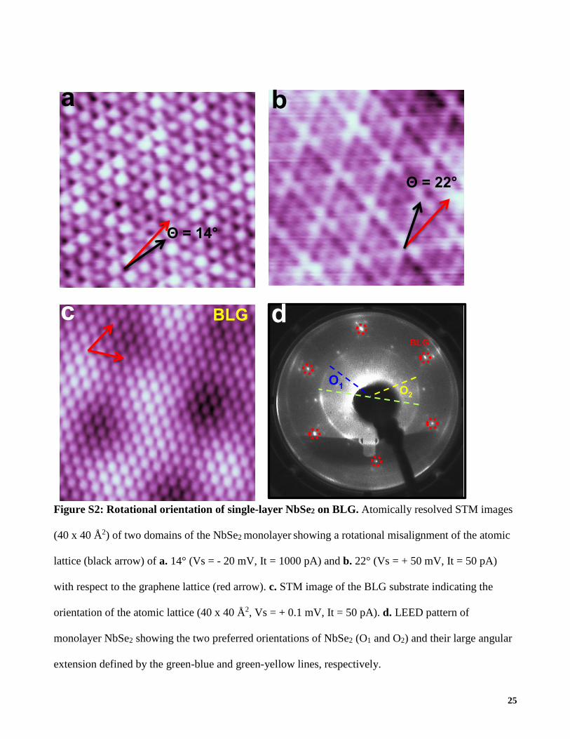
2. Rotational misalignment of single-layer NbSe2 on bilayer graphene
Consistent with our ARPES measurements, domains with multiple rotational alignments with
respect to the underlying BLG are seen in the STM images of ML NbSe2. Figs. S2a and S2b show
STM images taken on domains with 14o and 22o angles between the NbSe2 atomic lattice and the BLG
lattice, respectively. The black arrows lie along the NbSe2 lattice while the red arrows lie along the
BLG lattice. Fig. S2c shows an atomically-resolved STM image of the bare BLG substrate, with the
atomic lattice directions indicated by red arrows. The LEED pattern for a ML NbSe2 film is shown in
fig. S2d. The outer dots, circled in red, correspond to the BLG substrate and show well-defined
rotational alignment across the sample. The features corresponding to the NbSe2, however, appear as a
smeared-out circle. This circle is not completely isotropic and displays increased intensity
approximately every 30o. This is consistent with the ARPES measurements, which indicate two
dominant rotational domains separated by 30o. The observed rotational disorder is a consequence of
the weak interaction between the NbSe2 and the underlying BLG substrate and has been observed in
other monolayer TMD films grown on BLG.
25
Figure S2: Rotational orientation of single-layer NbSe2 on BLG. Atomically resolved STM images
(40 x 40 Å2) of two domains of the NbSe2 monolayer showing a rotational misalignment of the atomic
lattice (black arrow) of a. 14° (Vs = - 20 mV, It = 1000 pA) and b. 22° (Vs = + 50 mV, It = 50 pA)
with respect to the graphene lattice (red arrow). c. STM image of the BLG substrate indicating the
orientation of the atomic lattice (40 x 40 Å2, Vs = + 0.1 mV, It = 50 pA). d. LEED pattern of
monolayer NbSe2 showing the two preferred orientations of NbSe2 (O1 and O2) and their large angular
extension defined by the green-blue and green-yellow lines, respectively.
BLG c d
a b
Θ = 14°
Θ = 22°
BLG
O2 O
1
26
3. Transport measurements
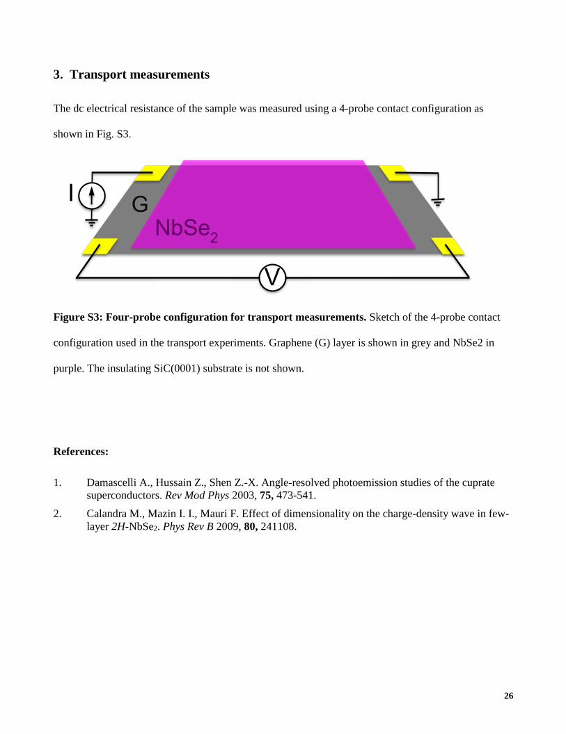
The dc electrical resistance of the sample was measured using a 4-probe contact configuration as
shown in Fig. S3.
Figure S3: Four-probe configuration for transport measurements. Sketch of the 4-probe contact
configuration used in the transport experiments. Graphene (G) layer is shown in grey and NbSe2 in
purple. The insulating SiC(0001) substrate is not shown.
References:
1. Damascelli A., Hussain Z., Shen Z.-X. Angle-resolved photoemission studies of the cuprate
superconductors. Rev Mod Phys 2003, 75, 473-541.
2. Calandra M., Mazin I. I., Mauri F. Effect of dimensionality on the charge-density wave in few-
layer 2H-NbSe2. Phys Rev B 2009, 80, 241108.
V
I
NbSe2
G