characterization of thin chromium coatings produced by pvd
TRANSCRIPT

Coatings 2021, 11, 215. https://doi.org/10.3390/coatings11020215 www.mdpi.com/journal/coatings
Article
Characterization of Thin Chromium Coatings Produced by PVD Sputtering for Optical Applications Andreia A. Ferreira 1, Francisco J. G. Silva 1,2,*, Arnaldo G. Pinto 1,2 and Vitor F. C. Sousa 1
1 School of Engineering, Polytechnic of Porto, Instituto Superior de Engenharia do Porto, Rua Dr. António Bernardino de Almeida, 431, 4200-072 Porto, Portugal; [email protected] (A.A.F.); [email protected] (A.G.P.); [email protected] (V.F.C.S.)
2 INEGI—Instituto de Ciência e Inovação em Engenharia Mecânica e Engenharia Industrial, Rua Dr. Roberto Frias, 400, 4200-465 Porto, Portugal
* Correspondence: [email protected]; Tel.: +351-2283-40500
Abstract: PVD (physical vapor deposition) and CVD (chemical vapor deposition) have gained greater significance in the last two decades with the mandatory shift from electrodeposition pro-cesses to clean deposition processes due to environmental, public safety, and health concerns. Due to the frequent use of coatings in several industrial sectors, the importance of studying the chro-mium coating processes through PVD–sputtering can be realized, investing in a real alternative to electroplated hexavalent chromium, usually denominated by chromium 6, regularly applied in elec-trodeposition processes of optical products in the automotive industry. At an early stage, experi-mental tests were carried out to understand which parameters are most suitable for obtaining chro-mium coatings with optical properties. To study the coating in a broad way, thickness and rough-ness analysis of the coatings obtained using SEM and AFM, adhesion analyzes with the scratch-test and transmittance by spectrophotometry were carried out. It was possible to determine that the roughness and transmittance decreased with the increase in the number of layers, the thickness of the coating increased linearly, and the adhesion and resistance to climatic tests remained positive throughout the study. Thus, this study allows for the understanding that thin multilayered Cr coat-ings can be applied successfully to polymeric substrates regarding optical applications in the auto-motive industry.
Keywords: PVD; sputtering; coatings; polymer coating; roughness; adhesion; transmittance; poly-carbonate; chromium; cleaner production
1. Introduction Aesthetic and product design issues are increasingly important in the automotive
market as well as in other industries in general. One of the processes with the greatest contribution to the aesthetic requirements of the products is galvanic chrome plating (electroplating). Thus, this work intends to provide an alternative solution to the chemical chrome plating process, which, according to Directive 2002/525/EC, should be eliminated by 2017 [1]. Additionally, the global REACH regulation argues that processes with hexa-valent chromium–chromium 6 should be completely abolished due to its extremely neg-ative and huge ecological footprint [2].
Physical vapor deposition (PVD) was only accepted in the 1960s [3] and its different variants have evolved more significantly in the last three decades [4,5]. In the PVD DC (Direct Current) magnetron sputtering process, the target material is transformed into atomic or molecular particles usually through the action of a physical thermal collision process of an inert gas, which directs the particles toward the substrates under high vac-uum conditions. The atomic particles condense and form a very thin coating [6]. The dep-osition rate, coating thickness, coating quality, and adhesion are parameters that have
Citation: Ferreira, A.A.;
Silva, F.J.G.; Pinto, A.G.; Sousa,
V.F.C. Characterization of Thin
Chromium Coatings Produced by
PVD Sputtering for Optical
Applications. Coatings 2021, 11, 215.
https://doi.org/10.3390/
coatings11020215
Academic Editor: Philipp Vladimiro-
vich Kiryukhantsev-Korneev
Received: 31 December 2020
Accepted: 9 February 2021
Published: 12 February 2021
Publisher’s Note: MDPI stays neu-
tral with regard to jurisdictional
claims in published maps and insti-
tutional affiliations.
Copyright: © 2021 by the authors. Li-
censee MDPI, Basel, Switzerland.
This article is an open access article
distributed under the terms and con-
ditions of the Creative Commons At-
tribution (CC BY) license (http://crea-
tivecommons.org/licenses/by/4.0/).

Coatings 2021, 11, 215 2 of 21
been continuously studied because small variations in process parameters can result in drastic changes in the characteristics of the final coating [7]. Some authors have been car-rying out experimental tests using the sputtering technique in order to be able to develop methods and new coatings on various substrates [8].
The literature directly related to the coating of polymeric substrates is very scarce. Moreover, Cr coatings have not been consistently applied in polymeric substrates, mainly out of the nitride form, with a clear gap in the literature regarding this issue.
The technique under study allows for the deposition of different metals on different substrates, most of them metallic. Martinho et al. [9] carried out a study on depositing thin films of TiAlCrSiN on the insert’s surface assembled into an injection mold (AISI P20), where it was realized that this coating promoted an increased wear resistance of about 50%, with practical tests managing to affirm that the coated surface showed no damage after 45,000 cycles of PP (Polypropylene) injection with 30% fiber glass as a reinforcement. It was possible to verify in another experimental study presented by Martinho et al. [10] that molds in AISI P20 provided with thin TiB2 PVD coatings showed slight detachment of that film after 90,000 injection cycles using the same reinforced polymer.
Fernandes et al. [11] performed a study comparing WC and CrCN in stamping dies (AISI D2) to avoid the adherence of the Sn usually present in tin sheet metal plates. After testing, the authors found that both coatings had good adhesion and good tribological properties, however, CrCN had a more regular and homogeneous morphology and is considered the best solution to avoid tin adhesion. Additionally, Alias et al. [12] studied silver/silver oxide and tantalum coatings deposited by sputtering on SS 316L parts. Through this study, the authors found that when the substrate was subjected to a heat treatment of 400 °C, the adhesion of the coatings was about 154% higher than in the un-coated condition, and that the coatings created exhibited an antibacterial performance su-perior to those usually applied, a property of high interest given its application on surgical instruments. The study presented by Mouche et al. [13] presented a characteristic of high interest with the deposition of Cr, CrN, and TiN films on substrates of a composite ceramic matrix (SiC) in order to study these coatings for a nuclear water reactor where the walls often crack. The authors concluded in the study that the coating using the three studied multilayered films was the most suitable to prevent and retard the propagation of cracks. Malvejerdi et al. [14] focused on the development of TiN coatings in Ck45 steel to increase the wear resistance and durability of tillage tools. After validations taken through tests carried out on clay soils, the authors confirmed that the coating had good quality, pro-moting the tool’s lifespan. Song et al. [15] intended to coat graphite substrates with tung-sten by CVD, however, given the chemical incompatibility between the different thermal expansion coefficients of the materials, the authors chose to adopt a new methodology that included coating the substrates with PVD using copper, and subsequently by CVD with tungsten. In this way, they managed to accommodate the stress of the interface and obtained an excellent adhesion. The work developed by Vӑnco et al. [16] focused on cov-ering natural fabrics, especially cotton. This fabric was coated with PVD with silver where excellent properties were obtained in the substrate + coating set, which allowed the au-thors to admit that they may be facing a new class of technical materials with these char-acteristics. Another example of the versatility of the sputtering method was presented by Rashid et al. [17] when they applied sputtering molybdenum films with different deposi-tion energies on glass substrates with soda and lime for photovoltaic applications. The results of the films’ characterizations revealed that they had a low surface roughness. Re-garding the deposition energies, the authors concluded that the films obtained with 100 W were the best option to manufacture solar cells in the future, given their refractive index of 5.41 in the visible range.
One of the most relevant investigations for this work was carried out by Konstantin et al. [18], who studied the relationship between wear and the number and thickness of the layers, with Ti + TiN, Ti + TiVN, Ti + TiZrN films on Ti–6Al–4V substrates. They con-cluded that the creation of multilayers was effective in increasing the resistance to erosion

Coatings 2021, 11, 215 3 of 21
wear. A decrease of 10× in the erosion rate of the samples with coatings provided with Ti and TiVN layers has been reported, concluding that the development of intermediate lay-ers is more favorable than the creation of a monolayer.
It is possible to find in the literature some studies on the sputtering deposition of coatings using polymeric materials as a substrate. These are briefly presented below to reveal again the versatility of the sputtering method. Coto et al. [19] conducted studies with multilayer Ti/TiN coatings by varying the thickness of the different layers between 1.5 μm and 11 μm on the polymeric substrates reinforced with carbon fiber. After several erosion, adhesion, and wear tests, the authors concluded that thin coatings failed due to the delamination of carbon fibers when exposed to erosion with sand, however, they re-vealed very good properties when subjected to rain erosion. Furthermore, it was observed that coatings with greater thicknesses were resistant to sand erosion. Zhang et al. [20] proved that CrN coatings are a promising alternative to Cr electroplating when deposited on ABS substrates, however, they cracked when subjected to climate change cycles. The authors studied the HiPIMS method to coat the ABS surface and in a comparative study, they concluded that the CrN coating deposited by HiPIMS had a higher corrosion and mechanical resistance than that applied by DCMS, making clear the possibility of this method to replace Cr electroplating in polymers. Qian et al. [21] deposited Ni thin films by sputtering in PC substrates to study the adhesion of the film as a function of the process parameters. Through micro-scratch equipment, the authors were able to state that the greater the ionization energy, the later the critical failure in the coating occurs, but in a larger study, the authors also performed plasma steps to increase the surface energy of the substrate and were able to conclude that this stage was the most important regarding the influence of the critical load that the coating is able to support, thus improving the adhesion between Ni and PC. Like Vergason et al. [22] referred to in their study, the Cr-6 applied in galvanic deposition should be abolished according to the REACH regulation and in that sense, they evaluated the properties of Cr deposited by sputtering in ABS for automotive applications and characterizing the obtained coating. Moreover, it was possi-ble to state that the Cr sputtered coating passed all OEM (Original Equipment Manufac-turers) automotive tests, showing that their thicknesses was in the nanometric scale, as opposed to the coatings obtained by galvanic deposition. Singh et al. [23] conducted stud-ies with metallic coatings by sputtering, namely aluminum on PC, where the optical re-sponses to the developed films were evaluated. The main conclusion drawn by the au-thors was related to the reflectance that reached 96% in all films at wavelengths from 250 nm to 2500 nm.
In summary, it is worth mentioning that most studies revealed the importance at-tributed to the different deposition parameters, considering that, according to the opinion and knowledge of each author, different values were attributed to the parameters. How-ever, and as above-mentioned, for each type of product, there must be a different deposi-tion recipe, which requires different deposition parameters, in order to obtain the best possible coating, considering the product requirements. To understand the capabilities of the developed coatings, they must be properly characterized, as can be seen in studies carried out by several authors. It is important to determine some properties of coatings such as the thickness of the coating, usually assessed by SEM (Scanning Electron Micros-copy) [9,24–30] to determine the surface roughness of the obtained coatings, which can be done using the atomic force microscopy (AFM) method [9,10], or measure/qualify the level of adhesion between the coating and the substrate, which can be carried out using scratch tests, classifying the adhesion according to the BS EN 1071-3: 2005 standard [31], to evaluate the transmittance, which can be obtained using spectrophotometry, or to test the resistance to climate change following the PV1200 standard [32].
The main goal of the work presented here is the development of thin chromium films that allow for a new class of products to be obtained that present surfaces with metallic luster as well as good mechanical and chemical properties, following some standards of the automotive industry. Since this study was aimed at optical parts, it is necessary to

Coatings 2021, 11, 215 4 of 21
understand the relationship between the coating thickness and the transmittance grade that the film can obtain. In this sense, a complete characterization of the films produced will also be performed.
2. Materials and Methods In this section, the materials used in this work are going to be described as well as
the methods used to characterize the coatings.
2.1. Substrates The substrate material used in this work was polymeric, more specifically, polycar-
bonate (PC). These parts were produced by injection molding. PC has some interesting properties such as its impact resistance, good electrical insulation properties, and high dimensional stability. Regarding the optical properties, this material presents a refraction index of 1.586 and 88% transmittance.
The samples used in this study (Figure 1) presented a flat geometry with dimensions of 147 mm × 54.5 mm and 3 mm thickness. The geometry of the samples was selected based on the molds available, taking into account that the samples must present a large flat surface, allowing us to cut different sub-samples in order to characterize the coatings after deposition. Moreover, the geometry of the samples should make it easier for their fixation and distribution into the PVD reactor without needing a special fixing system.
Figure 1. Industrial sample shape of the real part after the sputtering process.
2.2. Coating Deposition Coatings were produced using a Kolzer PVD deposition machine (Kolzer, Cologno
Monzese, MI, Italy), model MK63” with a deposition chamber volume of 1.02 m3, 10 kW power, and 1500 kJ ionization energy. This equipment is provided with hybrid capacity and is able to deposit aluminum by evaporation and other materials by the sputtering PVD technique. It has yet another function of high importance, PECVD, which allows de-positing polymer in the production cycle, promoting a barrier effect, and thus making the coating more chemical resistant. This equipment allows a first step of plasma to be per-formed to pre-treat the surface for 10 min, increasing its surface energy and, in this way, the adhesion of the coating to the substrate, eliminating some contaminants that may exist inside the deposition chamber and/or in the samples’ surface. Some factors were kept con-stant during the deposition process such as the type of gas used (argon with 99.998% pu-rity), the gas flow (440 sccm), and the bias (−25 V). Regarding the requested coatings, chro-mium targets with 99% purity were used. Each coating was produced by a certain number of layers, seeking the best solution to achieve the desired optical effect (metallization) and

Coatings 2021, 11, 215 5 of 21
the necessary transmittance. The deposition was made by steps, layer by layer, with inter-mediate steps of plasma cleaning. During the cleaning period, the shutters covered the targets, avoiding its deposition and allowing for the partial cooling down of the power system. This procedure is strongly recommended by the PVD equipment manufacturer to extend its lifespan. The deposition of each layer lasted 4 min, and the cleaning process between the layers’ deposition lasted 2 min. The chromium target used in the deposition process had the dimensions of 120 mm × 1000 mm × 16 mm and a weight of 14.20 kg, present-ing a chemical composition with a chromium content between 99.8–100%, which allows it to be defined as extra pure. The chemical composition of the target was collected from the datasheets of the supplier and can be seen in Table 1.
Table 1. Chemical composition of the chromium target.
Element PPM (Parts per Million) C 55 Ca 28 Fe 704 Mo 15 N 46 Nb 13 Ni 32 O 455 S 20 V 10 W 47 Cr Balance
One of the faces of each sample was masked in order to allow the passage of light, which is required regarding some of the tests that need to be carried out during the characterizations (transmittance).
2.3. Coating Characterization In order to assess whether the obtained coatings had the proper characteristics for
use in optical systems in the automotive industry, several characterizations were carried out using the most appropriate and available techniques. Thus, the thickness and chemical composition of the coating, adhesion to the substrate, morphology, resistance to changes in atmospheric conditions and transmittance were analyzed, since these are the character-istics that can most directly influence the performance of the coatings produced, consid-ering the market for which its development is intended. The different techniques used in this characterization are described below.
2.3.1. Coating Thickness The determination of the thickness of the different coatings was obtained using a FEI
Quanta 400FEG scanning electron microscope (SEM) (Field Electron and Ion Company, Hillsboro, OR, USA) provided with an EDAX Genesis X-Ray spectroscope (EDS—energy dispersive spectroscopy, EDAX), which allows two different image modes: secondary electrons (SE) and backscattered electrons (BSE). This equipment has a resolution of 1.2 nm. To analyze the samples under study, a working distance (WD) between 9 and 10 mm was used. In the specific case of this work, the back-scattered electrons mode was used, with a beam energy of 15 KeV. In order to carry out the most accurate analysis of the coatings’ thickness, the samples were previously cut and prepared, and then the samples were immersed in liquid nitrogen for 20 min, in order to allow a fracture as free as possible from plastic deformations.

Coatings 2021, 11, 215 6 of 21
2.3.2. Adhesion Analysis The adhesion between each coating and the substrate was assessed by scratch test
analysis using CSM REVETEST equipment (CSM Instruments, Peseux, Switzerland) fol-lowing the procedures recommended by the BS EN 1071-3:2005 standard [31]. Six scratches were made on each coating, allowing the most accurate results to be obtained. The Rockwell-I-119 indenter (EMCO Prüfmaschinen GmbH, Kellau, Kuchl, Austria) type was used to produce the scratches, applying an increasing normal load from 0 N to a final load of 10 N, considering the very soft polymeric substrate. The travelling speed selected for the indenter was 3 mm/min, and the final displacement was 10 mm. After we per-formed the tests, optical images of the scratches were taken using an optical microscope to have a first observation of the coatings’ behavior. These scratches were carefully ana-lyzed in order to correlate the distance covered by the indenter under the normal load. This analysis allows us to understand the type of failure that occurred, cohesive or adhe-sive, as well as the critical load that caused the failure. The software associated with the equipment produces a graph that allows for the evolution of the imposed normal load, the acoustic emission resulting from the contact between the indenter and sample, and the depth reached by the indenter to be observed. Combining the graphics referring to the test, namely, the acoustic emission (AE) and the optical images of the obtained grooves, it is possible to obtain the cohesive critical load (Fc) for each of the samples. After that, the samples were subjected to SEM analysis, looking for any special event. As no special events were found, a systematic observation was conducted in the middle and at the end of the grooves.
2.3.3. Roughness Determination Atomic force microscopy allows the morphological characterization of surfaces as
well as the measurement of surface roughness on a nanometric scale. This technique of surface analysis was used in this study in order to be able to assess and evaluate the rough-ness of the coated surfaces. For this purpose, VEECO—Multimode equipment (Wood-bury, Plainview, NY, USA) was used, which is equipped with a Nanoscope IV controller and Nanoscope 6.13 software. The selected surface area of analysis was 120 μm × 120 μm, with a maximum vertical displacement in the Z axis of 6 μm and a resolution of 16 bit. As for the contact, the radius of curvature of the indenter was less than 10 nm and there are three contact modes that can be used: contact, intermittent contact, and non-contact. The contact tip used in the analysis was silicon nitride with K = 0.32 N/m.
2.3.4. Climatic Change Resistance The tests in a climatic chamber aimed at reproducing in a laboratory environment
the climatic conditions that a product may be subjected to during its function. They intend to validate the ability of a product to resist natural causes such as temperature, humidity, salt fog, or UV radiation. To perform the test accordingly, a combination is required that exactly simulates the environmental conditions that the product may be subjected to, when in service. One of the regularly applied cycles was based on the automotive industry standard PV1200 standard for coated exterior parts. This standard belongs to Volkswagen and corresponds to a cycle presented in Figure 2.

Coatings 2021, 11, 215 7 of 21
Figure 2. Thermal cycle suggested by the PV1200 standard and applied in this study [32].
The climate change resistance test was carried out in a Weiss Technik (Weiss Um-welttechnik GmbH, Reiskirchen-Lindenstruth, Germany) climate chamber, model WK3-1500/70. This equipment requires a nominal current of 29 A and a nominal power of 13.8 kW and has internal chamber dimensions of 950 mm × 1100 mm × 1475 mm. The presented chamber also reaches a maximum temperature of 180 °C and a minimum temperature of −70 °C, combined with humidity control (blue line in Figure 2, which is another parameter of high interest.
2.3.5. Transmittance Analysis Spectrophotometry is a method capable of measuring the amount of light that is ab-
sorbed, transmitted, and reflected by a given sample, liquid or solid. To perform this type of test, a spectrometer is required, which can be provided with a single or double beam. From the tests carried out on this equipment, a spectrum results where the intensity by wavelength can be visualized. The selected wavelengths are usually found in the visible spectrum, that is, 350 nm to 750 nm. The presented method allows for the transmittance and direct and diffuse reflectance of a sample to be quantified. To measure transmittance and reflectance, two spectrophotometers were used as they allow for different measure-ments to be obtained. The Shimadzu UV-3600 (Shimadzu Corporation, Kyoto, Japan) does not allow direct measurements as it has an integrating sphere. The Shimadzu UV-1200 (Shimadzu Corporation, Kyoto, Japan) does not have an integrating sphere, so it only al-lows direct measurements. To obtain the measurements, a spectral resolution of 0.5 nm was applied in a spectral range of 350–800 nm.
3. Results and Discussion 3.1. Elementary Analysis
In the work carried out, an elementary analysis of the produced coatings was carried out, which allowed us to state that no contaminants were detected on the coatings, ensur-ing the purity of the films, as a result of the targets’ purity and absence of contaminants

Coatings 2021, 11, 215 8 of 21
inside the chamber. Figure 3 depicts the micro-analysis obtained for each set of layers considered in this work. The coating with six layers presents a more intense peak of C, resulting in the lower thickness of the coating and a higher detection of the substrate by the electron beam. This peak decreased with the increase in the number of layers (i.e., with the coating thickness). It is worth noting that the peak shown as O resulted from the over-lap of the chromium L peak by the O peak, and the presence of O resulted in the further contact of the Cr coating with the atmosphere. Moreover, as the electron beam potential used was 15 kV, an analysis depth of about 4 μm was expected, following a ‘pear’ shape, which clearly exceeded the thickness of the coating for any number of layers considered in this work, thus C is clearly felt in the spectrum. Furthermore, the intensity of the C peak decreased as the thickness of the Cr coating increased, as can be observed in the spectra of Figure 3. In fact, for six layers, the peak of C was predominant, since the thickness of the coating was lower. Thus, the relative intensity of the Cr and O peaks was lower than the C peak, although the O peak did not result solely from the influence of O, as previously justified by the reasons above-mentioned. When 10 layers of Cr were used, the intensity of the C peak was much smaller, as can also be seen in Figure 3 (last spectrum).
Figure 3. Spectrum obtained by scanning electron microscopy (SEM) energy dispersive spectroscopy (EDS) for samples of the films under study (6 layers, 8 layers, and 10 layers).
Although the EDS technique only allows for a semi-quantitative analysis of the coat-ings’ composition, Table 2 describes the values obtained through this analysis. As can be seen in Table 2, where two different analyses are presented (considering C, or not consid-ering the C substrate), the relation between Cr and O remained almost the same when analyzing just these two elements for the different number of layers considered in this work. Moreover, the O usually brings some uncertainties in these analyses due to its na-ture when analyzed by electron beams.

Coatings 2021, 11, 215 9 of 21
Table 2. Semi-quantitative analysis of the coatings composition carried out by energy dispersive spectroscopy (EDS).
Cr Coating Layers Semi-Quantitative Composition (wt%) – Element Considering C Do not Considering C – Cr 42.75 78.85 6 Layers O 22.31 21.15 – C 34.94 – – Cr 51.94 78.11 8 Layers O 23.56 21.89 – C 24.50 – – Cr 67.85 80.36 10 Layers O 20.84 19.64 – C 11.31 –
3.2. Coating Thickness Using SEM, it was found that the greater the number of layers deposited, an increase
in the thickness of the coating occurred, being possible to observe that each layer was approximately 25 nm in thickness. As for the thickness of the coating, samples provided with 6, 8, and 10 layers were produced and analyzed, whose optical images are shown in Figure 4. The multilayer classification was adopted for the studied coating, taking into account its deposition method. The procedure imposed by the deposition equipment in-cludes a series of deposition steps that form a cycle. However, no interface can be detected because the process is continuous with the deposition–cleaning–deposition steps until reaching the desired number of layers. It is important to note that the cleaning step pre-vents overheating of the power supply and promotes the adhesion of different layers of Cr, which were about 25 nm thick. In order to observe some of the interface between the layers, XRD analyzes were attempted, but due to the extremely reduced thickness of the coatings, it was not possible to effectively detect the Cr spectrum. Therefore, the term “multilayer” may not be the most appropriate according to the current literature, since it is usually associated with layers with different materials and different thicknesses. How-ever, given the experimental methodology including several layers of the same material and the number of layers being one of the topics under study, the term “multilayer” is, therefore, considered to be the most suitable for this study.
Figure 4. Cross-section view of the films obtained using 10 kW power in the samples with 6, 8, and 10 layers of chromium.
Considering Figure 4, it can be reported that with six layers, the average thickness of the complete coating was 150 nm, with eight layers a value of 200 nm was obtained, and with 10 layers, an average value of 250 nm was achieved, which proved that each layer was about 25 nm thick. Moreover, the repeatability found for samples with the same num-ber of layers proved to be quite high, thus ensuring that the process is reliable in terms of

Coatings 2021, 11, 215 10 of 21
the thickness of the coatings obtained. Moreover, the results presented the desired linear-ity in the thickness growth with the increase in the number of layers.
Some tests of the same coating were carried out with 6 kW of deposition power, which can be seen in Figure 5. Indeed, the depositions carried out using 10 kW revealed a clear higher thickness, but the same structure and level of roughness. The real difference between them was that the coatings obtained under 6 kW allowed for the required trans-mittance, whereas the coatings obtained with 10 kW did not allow the required transmit-tance.
Figure 5. Cross-section view of the films obtained using 6 kW power. In view we can see the samples with 6, 8, and 10 layers of thickness.
Considering the study carried out in terms of the thickness of the different coatings and taking into account Figure 4, referring to samples produced with 10 kW power, and Figure 5 with results of 6 kW power, Table 3 was obtained with the measurements made over the studied samples with the analysis of three samples per coating.
Through the SEM equipment, it was possible to obtain the measurements shown in Table 3. Carrying out a brief comparison between the presented values, it was noticed that with 6 kW power, the average thickness of each layer was approximately 15 nm, while when the power increased to 10 kW, a thickness per layer of 25 nm was observed. Thus, it can be concluded that the increase in deposition power causes an increase in the thick-ness of the coating by approximately 50%, revealing a considerable increase in the Cr dep-osition rate.
Table 3. Thicknesses of the thin coatings obtained through scanning electron microscopy (SEM).
Reference Thickness [nm] Standard Deviation [nm] 6 Layers 149.2 0.010 8 Layers 190.0 0.014 10 Layers 249.1 0.018 6 Layers (6 kW) 105.3 0.032 8 Layers (6 kW) 157.4 0.026 10 Layers (6 kW) 189.1 0.019
3.3. Roughness Determination The surface roughness of the samples was obtained with the aid of the AFM, making
the measurement in three samples of each test reference. It was possible to determine that the greater the number of deposited layers, the lower the surface roughness of the samples under study, however, it should be noted that even in the uncoated samples, the surface roughness was very small, always lower than 5 nm (Ra parameter). The results of the roughness analysis by AFM are depicted in Table 4.

Coatings 2021, 11, 215 11 of 21
Table 4. Roughness characterization of the coatings.
Reference Ra [nm] Standard DeviationRa [nm] Rt [nm]
Standard Deviation Rt [nm] Rq [nm]
Standard Deviation Rq [nm]
Substrate 5.77 0.032 100 0.043 6.72 0.036 6 Layers 4.19 0.043 53 0.021 5.55 0.026 8 Layers 3.29 0.038 65 0.036 4.27 0.038 10 Layers 1.94 0.027 20 0.019 2.49 0.031
In fact, Table 4 shows a decrease in surface roughness from samples “Substrate” to samples “10 Layers”, while there was also an increase in the number of deposited layers. A homogenization of the surface was observed, making the surface more uniform and with less scratches or micro craters. A 3D image of some of the surfaces under analysis was generated in the AFM NanoScope® 6.13 software in order to visualize both homoge-neity and the size of the peaks and valleys as well as their frequency. Figure 6 also allows us to understand the different values reported in Table 4.
(a)
(b)
(c)
Figure 6. 3D topography analysis of samples. Six layers (a), eight layers (b), and 10 layers (c) using atomic force microscopy (AFM) over an area of 20 × 20 μm2.
In Figure 6, it is possible to conclude in a visual way that the increase in the number of deposited layers contributed significantly to the homogenization of the surface, because the posterior layers tended to minimize some existing scratches and micro-voids present on the last deposited layer, contributing significantly to the uniformity of the final layer.

Coatings 2021, 11, 215 12 of 21
3.4. Adhesion Analysis To assess the adhesion of the coating to the substrate, the scratch-test was performed,
where the grooves presented were obtained and visible in Figure 7. As can be seen in Figure 7, the scratches were smooth, showing some lateral cracking, which decreases with the increase in the number of layers. This phenomenon deserves SEM analysis, which will be presented later in this work.
Figure 7. Some images of the scratches resulting from the scratch test to the “6 Layers” to “10 Layers” batch samples, obtained with an optical microscope.
Through the scratch tests, it was observed that the failures that occurred were of a cohesive nature and not adhesive, which does not compromise the viability of the devel-oped films and their compatibility with the substrate. In fact, in these samples it is possible to observe lateral micro-cracks in semicircles on the coatings due to bow deformation, properly cataloged in the BS EN 1071-3:2005 standard [31]. These samples presented very good adhesion, which was confirmed by the images of the scratches obtained. The number of deformations (lateral cracks) observed can be originated by the level of stresses to which the coating is subjected during the indenter travel and under the normal load imposed. One of the most important questions in the present study focused on the relationship of adhesion with the increase in the number of layers. Observing Figure 8, it can be seen that the acoustic emission (AE) signal remained smooth in all tests, showing that no critical events were reported during the indenter travel. However, the penetration depth corre-sponding to the deformation of the substrate can be seen, which caused the lateral cracks previously referred.
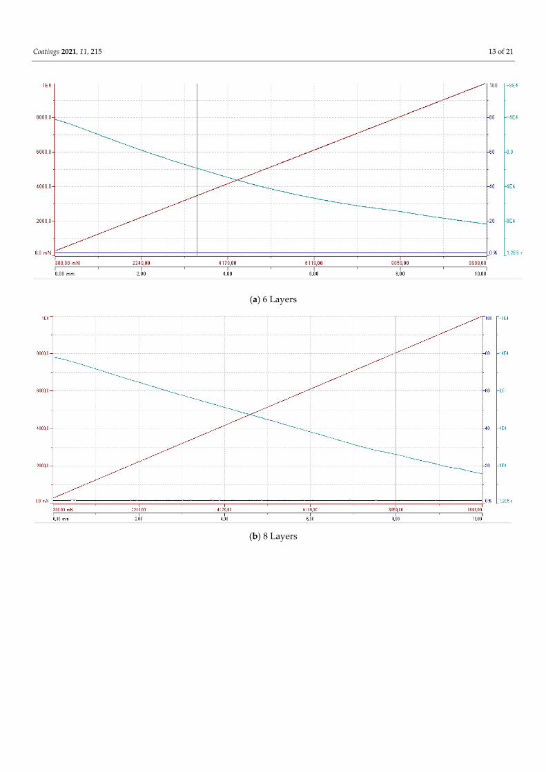
Coatings 2021, 11, 215 13 of 21
(a) 6 Layers
(b) 8 Layers

Coatings 2021, 11, 215 14 of 21
(c) 10 Layers
Figure 8. Acoustic emission (AE) graphs obtained when performing the scratch test for the studied samples: (a) 6 layers, (b) 8 layers, (c) 10 layers.
In the graphs representing the path of the indenter in Figure 8, the line representing the normal load is displayed in red, in blue the AE, and in green the penetration depth. Looking at the AE graphs and Figure 7, it can be concluded that there were no significant breaks during the sliding of the indenter tip, which corroborates the information pre-sented previously. When comparing the results obtained with the atlas presented in the BS EN 1071-3:2005 standard [31], it can be concluded that the failures that occurred were of type (a), defined as cracking by bow deformation. These cracks had a geometry that accompanied the accumulation of material in front of the indenter, forming semicircular trajectories parallel to the contact surface of the tip, and were presented as cohesive fail-ures, not compromising the adhesion of the coating. Thus, while there was no detachment of the coating, these failures can be admitted as cohesive. Hence, good adhesion between the Cr coatings and the substrate seems to be ensured. Analyzing the grooves promoted by the indenter in depth, SEM observations were made throughout all scratches, trying to find special events. As no relevant special events were found, systematic pictures of two specific areas were taken: in the middle of the groove and at the end of the same. The pictures are depicted in Table 5.

Coatings 2021, 11, 215 15 of 21
Table 5. Detailed images of the scratches produced during the scratch-tests (general magnifica-tion: 500×).
Scratch Detailed Images During Indenter Travel Path End of the Scratch
6 layers
8 layers
10 lay-ers
As can be seen from Table 5, no detachments were observed. However, due to the punctual pressure produced by the indenter during its travel, and also due to the substrate deformation, some coating cracks could be observed, but without detachment, which showed the good adhesion evidenced by the coating to the polymeric substrate. As the thickness of the coating increased, the frequency of ‘shrapnel’ produced on the coating decreased, and a new phenomenon occurred: the cracks decreased in number and in-creased in intensity. The coating with 10 layers showed a higher mechanical strength, which increased more significantly from eight to 10 layers. The lateral cracking initially observed for six layers tended to dissipate with the increase in the number of the layers. Thus, small phenomena of cohesive failure occurred, not showing significant events in AE signal, but no adhesive failures could be detected. Excellent adhesion of the Cr coating to the substrate was confirmed by EDS analysis, as can be seen in Figure 9.

Coatings 2021, 11, 215 16 of 21
(a)
(b) (c)
Figure 9. Energy dispersive spectroscopy (EDS) analysis of a scratch groove with (a) a partial groove view of a 10 layers coating, (b) spectrum of the external scratch area (Z1), and (c) internal scratch area (Z2).
3.5. Climatic Chamber The tests in the climatic chamber were carried out following the PV1200 standard,
where humidity and temperature are controlled, and it can be observed that all PC sam-ples with the different coatings were able to withstand the imposed working loads with-out chromium fragmentation.
As for the tests in the climatic chamber, it was concluded that the Cr coating with six, eight, and 10 layers gives rise to a product compatible with polymeric PC substrates. In-deed, the samples did not show any fragmentation of the coating, neither during or after the PV1200 cycle, and the coating did not show changes in its color or tonality, thus ad-mitting the viability of this coating and the ability to respond in the most appropriate way to the demands of both temperature and humidity.
3.6. Transmittance Analysis Keeping the focus on the primary purpose of the study, it is of utmost importance to
determine the transmittance, relating it to the number of coating layers because it is de-duced that the greater the number of layers, the lower the transmittance. However, it is important to be able to quantify this decrease and be able to relate it for a more accurate characterization of the coating. Since the main goal of this work was to develop coated optical parts, it is important to carry out an assessment of the transmittance obtained with

Coatings 2021, 11, 215 17 of 21
the coatings under study. In Figure 10, the transmittances evolution can be observed, de-pending on the wavelength.
Figure 10. Transmittance by wavelength of the samples under study.
However, the graph presented was related to specific wavelengths and was intended to obtain the transmittance of the sample to white light, using in this case, the spectrum related to an Illuminant A, and the integral function of an Illuminant A must be calculated as well as the integrals of the functions shown in Figure 10. Finally, a division was made between the integral of Illuminant A and the integral of the corresponding curve, where the transmittance of each sample was obtained for an Illuminant A light, as shown in Fig-ure 11.
Figure 11. Relative distribution of spectral power for an Illuminant A light in the studied samples between 350 nm and 750 nm.
In the curves represented in Figure 11, the real distribution graph is visualized, which relates the spectral power of an Illuminant A light to the respective wavelengths. By ana-lyzing the graph represented, the actual transmittance values shown in Table 6 can be obtained.
Table 6. Real transmittance of the studied samples.
Reference Transmittance (%) 6 Layers 0.40% 8 Layers 0.23% 10 Layers 0.01%

Coatings 2021, 11, 215 18 of 21
It is important to state that with the values presented, it is very difficult to obtain an optical part, given the very low transmittance obtained. However, it was also possible to understand that these practically zero values reflected the deposition power employed, which was relatively high (10 kW). Thus, it is vital to analyze lower power values that produce mirrored samples, but that can be backlit. In order to understand the influence of the deposition power on the transmittance obtained by the samples, new samples (EP6, EP8, and EP10) were coated with 6 kW of deposition power and the transmittance for each sample was analyzed. These values are shown in Table 7.
Table 7. Transmittance ratio obtained with 6 kW of power and 10 kW of power.
Reference 6 kW Sample Transmittance (%) Reference 10 kW Sample Transmittance (%) Delta 6 Layers (EP6) 8.78% 6 Layers 0.40% 8.38% 8 Layers (EP8) 3.90% 8 Layers 0.23% 3.67%
10 Layers (EP10) 2.00% 10 Layers 0.01% 1.99%
As shown in Table 7, the difference in transmittance between samples that can be compared was very high. Thus, it can be concluded that the ideal to achieve acceptable levels of transmittance would be to maintain the deposition power at 6 kW and apply only six layers of chromium. To obtain the planned samples (EP6, EP8, and EP10), the only parameter changed was the deposition power. The other parameters remained the same as the recipe used for the first batches of samples.
In short, it was possible through this study to understand a little more widely the chromium coatings produced by sputtering in polymeric parts. To carry out this study, several deposition programs were developed to understand the effect of each parameter on the obtained coating. After obtaining the desired visual aspect, deposition was per-formed, changing only the number of layers of coating to be applied and its characteriza-tion was carried out, as shown above. In Figure 12, it is possible to observe samples with different deposition layers.
Figure 12. Sequential staining image of six to 10 layers to chromium.
The discussion presented in the current work is relatively brief given the current ab-sence of studies that can be compared with the samples developed in this work. It was concluded that the state-of-the-art regarding thin chromium coatings on polymeric sub-strates for optical parts presents a huge gap.
4. Conclusions The deposition of three different thicknesses of chromium coatings was carried out
on PC injection molded substrates. These coatings differed in the number of layers of chro-mium that made up the coating, and this distinction allowed us to obtain completely dif-ferent coatings with the same material, as can be seen in Figure 12. These coatings were widely characterized to understand their feasibility for application in polymeric parts,

Coatings 2021, 11, 215 19 of 21
with a mirrored appearance but with the possibility of being backlit, opening a new range of products for the automotive market. After all analyses and tests, some conclusions can be drawn, as follows: • Cr coatings of different layers have an excellent adhesion to PC substrates, proven
by the absence of adhesive failures after performing the scratch tests. However, the adhesion decreased when the number of Cr layers increased, this means, the higher the coating thickness, the lower the adhesion. However, regarding the maximum number of layers used in this work (10 layers), the adhesion remained at perfectly acceptable levels;
• With the parameters defined for the process (10 kW power), it was determined that each coating layer was approximately 25 nm thick, which proves that very thin chro-mium films can be deposited in polymeric substrates using the sputtering technique;
• The surface roughness of the samples with the different layers of coatings assessed by AFM was very low, approximately 3 nm (Ra). Moreover, a decrease in surface roughness with the increase in the number of deposition layers has been reported;
• The chromium coating was shown to be compatible with the PC substrate. This com-bination was able to withstand the climatic tests under the condition imposed by the PV1200 standard, and has not been reported to have any functional problem to the coating;
• The transmittance seems to be affected by the different number of layers, but the dif-ferent number of layers does not present significant differences in terms of adhesion to the substrate. Moreover, the transmittance slightly increased from 10 kW to 6 kW, so the change was enough to allow its application in optical automotive systems; and
• Regarding the possibility of the samples being able to be backlit, the results obtained with the transmittance allowed us to realize that with the deposition parameters cho-sen, the optical capacity of the samples was almost null. However, with small changes in the parameters (power), it was possible to obtain optical samples. Thus, considering these results, it is admitted that in fact, the chromium coating pro-
duced by sputtering can industrially be a substitute process for chromium electroplating, allowing parts with great visual aspect and homogeneous coating on the entire surface to be obtained. This way of production is much more environmentally friendly and allows for compliance with the soon to be imposed regulations. However, regarding the produc-tion of optical parts for the automotive industry to be backlit, more studies should be car-ried out in future in order to investigate the best condition to obtain a really good com-promise between adhesion and transmittance.
Through the work presented, it was possible to confirm that coatings made by the PVD sputtering process without harming the environment can be produced to optical au-tomotive systems in detriment of the Cr-6 electroplated coatings. Indeed, the electroplated Cr-6 coatings are harmful to public health and the environment.
Author Contributions: Conceptualization, F.J.G.S.and A.A.F.; methodology, F.J.G.S.; validation, F.J.G.S., A.G.P.and V.F.C.S.; formal analysis, A.G.P.; investigation, A.A.F and V.F.C.S.; resources, A.A.F., A.G.P., F.J.G.S.and V.F.C.S.; data curation, A.G.P.; writing—original draft preparation, A.A.F.; writing—review and editing, F.J.G.S., A.G.P.and V.F.C.S.; visualization, A.G.P.; supervision, F.J.G.S.; project administration, A.A.F.and F.J.G.S.; All authors have read and agreed to the pub-lished version of the manuscript.
All authors have read and agreed to the published version of the manuscript.
Funding: This research received no external funding.
Data Availability Statement: No new data were created or analyzed in this study. Data sharing is not applicable to this article.
Acknowledgments: The authors would like to thank Prof. António Bastos from the University of Aveiro for his support in making available some of the equipment used in this study. Moreover, his

Coatings 2021, 11, 215 20 of 21
team research is also acknowledged. The authors would like to thank Rui Rocha from CEMUP for his commitment in helping with the interpretation of the SEM, EDS, and AFM results. The authors would like to thank INEGI for its support in the current research activities.
Conflicts of Interest: The authors declare no conflicts of interest.
References 1. American Chemistry Council. Regulation (CE) n.o 1907/2006 of the European Parlamient, 18th of December, 2006. Off. J. Eur.
Union 2011, 396/3. Available online: https://eur-lex.europa.eu/eli/reg/2006/1925/oj. (accesed on 21st December 2020). 2. Comissão das Comunidades Europeias. In Análise Ambiental; 2005 (In Portuguese). Available online: https://eur-lex.eu-
ropa.eu/LexUriServ/LexUriServ.do?uri=COM:2005:0017:FIN:PT:PDF. (accesed on 17th December 2020). 3. Berhaus, B. Improvements in and Relating to the Coating of Articles by Means of Thermally Vaporized Material. UK Patent,
Nr. 510, 18 March 1993. 4. Baptista, A.; Silva, F.; Porteiro, J.; Míguez, J.; Pinto, G. Sputtering Physical Vapour Deposition (PVD) Coatings: A Critical Review
on Process Improvement and Market Trend Demands. Coatings 2018, 8, 402, doi:10.3390/coatings8110402. 5. Silva, F.J.G. Revestimentos Duros e Ultra-Duros Executados No Vácuo. Ph.D. Thesis, FEUP—Faculty of Engineering, University
of Porto, Porto, Portugal, 2001. (In Portuguese). 6. Mattox, D.M. The Foundations of Vacuum Coatings Technology; Noyes Publications: NJ, USA, 2003; pp. 66. 7. Barshilia, H.C.; Ananth, A.; Khan, J.; Srinivas, G. Ar + H2 plasma etching for improved adhesion of PVD coatings on steel
substrates. Vac. 2012, 86, 1165–1173, doi:10.1016/j.vacuum.2011.10.028. 8. Baptista, A.; Silva, F.J.G.; Porteiro, J.; Míguez, J.L.; Pinto, G.; Fernandes, L. On the physical vapour deposition (PVD): Evolution
of Magnetron Sputtering Processes for Industrial Aplications, Procedia Manuf. 2018, 17, 746–757. 9. Martinho, R.; Andrade, M.; Silva, F.; Alexandre, R.; Baptista, A. Micro-abrasion wear behaviour of TiAlCrSiN nanostructured
coatings. Wear 2009, 267, 1160–1165, doi:10.1016/j.wear.2008.12.063. 10. Martinho, R.P.; Silva, F.J.G.; Alexandre, R.J.D.; Baptista, A.P.M. TiB2 Nanostructured Coating for GFRP Injection Moulds. J.
Nanosci. Nanotechnol. 2011, 11, 5374–5382, doi:10.1166/jnn.2011.3772. 11. Fernandes, L.; Silva, F.; Paiva, O.; Baptista, A.; Pinto, G. Minimizing the Adhesion Effects in Food Packages Forming by the Use
of Advanced Coatings. Procedia Manuf. 2018, 17, 886–894, doi:10.1016/j.promfg.2018.10.141. 12. Alias, R.; Mahmoodian, R.; Genasan, K.; Vellasamy, K.M.; Shukor, M.H.A.; Kamarul, T. Mechanical, antibacterial, and bio-
compatibility mechanism of PVD grown silver–tantalum-oxide-based nanostructured thin film on stainless steel 316L for sur-gical applications. J. Pre-Proof. 2020, 107, 54.
13. Mouche, P.; Ang, C.; Koyanagi, T.; Doyle, P.; Katoh, Y. Characterization of PVD Cr, CrN, and TiN coatings on SiC. J. Nucl. Mater. 2019, 527, 151781, doi:10.1016/j.jnucmat.2019.151781.
14. Malvajerdi, S.S.; Malvajerdi, A.S.; Ghanaatshoar, M. Protection of CK45 carbon steel tillage tools using TiN coating deposited by an arc-PVD method. Ceram. Int. 2019, 45, 3816–3822, doi:10.1016/j.ceramint.2018.11.051.
15. Song, J.; Lian, Y.; Lv, Y.; Liu, J.; Yu, Y.; Liu, X.; Yan, B.; Chen, Z.; Zhuang, Z.; Zhao, X.; et al. Development of CVD-W coatings on CuCrZr and graphite substrates with a PVD intermediate layer. J. Nucl. Mater. 2014, 455, 531–536, doi:10.1016/j.jnucmat.2014.08.027.
16. Vančo, M.; Krmela, J.; Pešlová, F. The use of PVD coating on natural textile fibers. Procedia Eng. 2016, 136, 341–345. 17. Rashid, H.; Rahman, K.S.; Hossain, M.I.; Nasser, A.A.; Alharbi, F.H.; Akhtaruzzaman; Amin, N. Physical and electrical proper-
ties of molybdenum thin films grown by DC magnetron sputtering for photovoltaic application. Results Phys. 2019, 14, 7, doi:10.1016/j.rinp.2019.102515.
18. Selivanov, K.S.; Smyslov, A.M.; Dyblenko, Y.M.; Semenova, I.P. Erosive wear behavior of Ti/Ti(V,Zr)N multilayered PVD coat-ings for Ti-6Al-4V alloy. Wear 2019, 160–166, doi:10.1016/j.wear.2018.11.016.
19. Coto, B.; Hallander, P.; Mendizabal, L.; Pagano, F.; Kling, H.; Ortiz, R.; Barriga, J.; Selegård, L. Particle and rain erosion mecha-nisms on Ti/TiN multilayer PVD coatings for carbon fibre reinforced polymer substrates protection. Wear 2021, 466, 203575, doi:10.1016/j.wear.2020.203575.
20. Zhang, D.; Zuoa, X.; Wanga, Z.; Lia, H.; Chena, R.; Wang, A.; Ke, P. Comparative study on protective properties of CrN coatings on the ABS substrate by DCMS and HiPIMS techniques.Surf. Coat. Technol. 2020, 394, 7.
21. Qian, X.; Pang, X.; Gao, K.; Yang, H.; Jin, J.; Volinsky, A.A. Adhesion of Sputtered Nickel Films on Polycarbonate Substrates. J. Mater. Eng. Perform. 2013, 23, 786–790, doi:10.1007/s11665-013-0806-6.
22. Vergason, G.; Fitch, M.; Smith, R.; Brazil, M.; Jochum, T. PVD Chromium Coatings Replacing Decorative Chromium Elec-tro-plated Coatings on Plastics. Soc. Vac. Coaters 2015, 403–410. doi: dx.doi.org/10.14332/svc15.proc. 1971.
23. Singh, M.M.; Vijaya, G.; Krupashankara, M.S.; Sridhara, B.K.; Shridhar, T.N. Studies on Nanostructure Aluminum Thin Film Coatings Deposited using DC magnetron Sputtering Process. Mat. Sci. Eng. 2016, 149, 10.
24. Silva, F.; Baptista, A.; Pereira, E.; Teixeira, V.; Fan, Q.; Fernandes, A.; Costa, F. Microwave plasma chemical vapour deposition diamond nucleation on ferrous substrates with Ti and Cr interlayers. Diam. Relat. Mater. 2002, 11, 1617–1622, doi:10.1016/s0925-9635(02)00029-8.
25. Martinho, R.; Silva, F.; Baptista, A. Wear behaviour of uncoated and diamond coated Si3N4 tools under severe turning condi-tions. Wear 2007, 263, 1417–1422, doi:10.1016/j.wear.2007.01.048.

Coatings 2021, 11, 215 21 of 21
26. Silva, F.; Fernandes, A.; Costa, F.; Teixeira, V.; Baptista, A.; Pereira, E. Tribological behaviour of CVD diamond films on steel substrates. Wear 2003, 255, 846–853, doi:10.1016/s0043-1648(03)00145-5.
27. Silva, F.; Fernandes, A.; Costa, F.; Baptista, A.; Pereira, E. Unstressed PACVD diamond films on steel pre-coated with a compo-site multilayer. Surf. Coatings Technol. 2005, 191, 102–107, doi:10.1016/j.surfcoat.2004.02.036.
28. Silva, F.J.G.; Neto, M.A.; Fernandes, A.J.S.; Costa, F.M.; Oliveira, F.J.; Silva, R.F. Adhesion and Wear Behaviour of NCD Coatings on Si3N4 by Micro-Abrasion Tests. J. Nanosci. Nanotechnol. 2009, 9, 3938–3943, doi:10.1166/jnn.2009.ns93.
29. Martinho, R.P.; Silva, F.J.G.; Martins, C.; Lopes, H. Comparative study of PVD and CVD cutting tools performance in milling of duplex stainless steel. Int. J. Adv. Manuf. Technol. 2019, 102, 2423–2439, doi:10.1007/s00170-019-03351-8.
30. Silva, F.J.G.; Martinho, R.P.; Martins, C.; Lopes, H.; Gouveia, R.M. Machining GX2CrNiMoN26-7-4 DSS Alloy: Wear Analysis of TiAlN and TiCN/Al2O3/TiN Coated Carbide Tools Behavior in Rough End Milling Operations. Coatings 2019, 9, 392, doi:10.3390/coatings9060392.
31. BS EN 1071-3:2005. Advanced Technical Ceramic—Methods of Test for Ceramic Coatings. Part 3: Determination of Adhesion and Other Mechanical Failure Modes by Scratch Test 2005. Technical Committee RPI/13, British Standard, UK. London, 2005.
32. Automotive Parts—Weather Resistance Test—PV1200 2004, Central de Normas Volkswagen. Peças Automotivas—Teste de Resistência à Alternância de Clima; Volkswagen Standard Center; Porto, Portugal, 2004. (In Portuguese).