characterization of various antenna ... of various antenna structures used for device illumination...
TRANSCRIPT

CHARACTERIZATION OF VARIOUS
ANTENNA STRUCTURES USED FOR DEVICE
ILLUMINATION
by
Peter Marcus Buff III
A thesis submitted to the Graduate Faculty ofNorth Carolina State University
in partial fulfillment of therequirements for the Degree of
Master of Science
Electrical Engineering
Raleigh
May 2003
APPROVED BY:
Chair of Advisory Committee
ABSTRACT
P Mark Buff. Characterization of Various Antenna Structures Used for DeviceIllumination. (Under the direction of Dr. Michael B. Steer.)
A non-intrusive approach for personal surveillance is explored. A potential strat-
egy for identification of electronic devices using electromagnetic illumination with
the aim of identifying unique resonances and signatures is presented. The concept
is that signatures can be compared to a known signature for a particular device. If
discrepancies are detected, then the device may be flagged as a suspect item. Var-
ious antenna structures are analyzed to determine the ideal antenna characteristics
needed for electromagnetic illumination. A double ridged horn antenna is designed,
characterized and compared to a conical spiral right hand circular polarized antenna
and a standard gain antenna. Various passive structures and electronic devices are
illuminated with electromagnetic energy and responses analyzed.

ii
To my dear wife Christine

iii
BIOGRAPHY
Mark Buff was born in Warner Robins, Georgia, USA into an Air Force Family
and has lived in numerous states and countries. He received his Bachelors Degree
in Electrical Engineering from North Carolina State University in 1994, where soon
after, he was employed by Alcatel Network Systems in Raleigh. There, he worked
on fiber optic multiplexing transport systems and digital cross connect switches. He
returned to North Carolina State University in the Fall of 2001 to pursue a Master’s
Degree in Electrical and Computer Engineering.

iv
ACKNOWLEDGEMENTS
I would like to express my deepest thanks and love to my wife who has sacrificed
countless nights and weekends for the success of my education.
I take this opportunity to thank my advisor, Professor Michael Steer for his in-
valuable guidance and vivacity. I am looking forward to pursuing my doctorate under
his direction. In addition, thanks goes to my thesis committee, Dr. Hamid Krim and
Dr. Doug Barlage.
Thanks to my bright and talented lab friends whom all have acted as great sources
of energy, ideas and camaraderie.
Thanks to my gracious parents for all of your support.

v
Contents
List of Figures vii
1 Introduction 11.1 Motivation . . . . . . . . . . . . . . . . . . . . . . . . . . . . . . . . . 11.2 Thesis Overview . . . . . . . . . . . . . . . . . . . . . . . . . . . . . . 2
2 Existing Surveillance Technologies 42.1 Introduction . . . . . . . . . . . . . . . . . . . . . . . . . . . . . . . . 42.2 X-Ray Imaging Systems . . . . . . . . . . . . . . . . . . . . . . . . . 42.3 Metal Detecting Systems . . . . . . . . . . . . . . . . . . . . . . . . . 72.4 Millimeter Wave Imaging . . . . . . . . . . . . . . . . . . . . . . . . . 92.5 Chemical Trace Detection Systems . . . . . . . . . . . . . . . . . . . 12
3 Detection 143.1 Approach . . . . . . . . . . . . . . . . . . . . . . . . . . . . . . . . . 143.2 Antenna Parameters . . . . . . . . . . . . . . . . . . . . . . . . . . . 14
3.2.1 Radiation Pattern . . . . . . . . . . . . . . . . . . . . . . . . . 163.2.2 Field Regions . . . . . . . . . . . . . . . . . . . . . . . . . . . 163.2.3 Directivity, Gain and Antenna Efficiency . . . . . . . . . . . . 193.2.4 Bandwidth . . . . . . . . . . . . . . . . . . . . . . . . . . . . . 203.2.5 Input Impedance . . . . . . . . . . . . . . . . . . . . . . . . . 20
3.3 Antennas of Interest . . . . . . . . . . . . . . . . . . . . . . . . . . . 203.3.1 Standard Gain Horn . . . . . . . . . . . . . . . . . . . . . . . 203.3.2 Conical Spiral . . . . . . . . . . . . . . . . . . . . . . . . . . . 213.3.3 Double Ridged Horn . . . . . . . . . . . . . . . . . . . . . . . 23
3.4 Reflection and Transmission of EM Waves . . . . . . . . . . . . . . . 273.5 Network Analyzer Calibration . . . . . . . . . . . . . . . . . . . . . . 303.6 Summary . . . . . . . . . . . . . . . . . . . . . . . . . . . . . . . . . 30
4 Antenna Characterization Results 314.1 Time Gating . . . . . . . . . . . . . . . . . . . . . . . . . . . . . . . . 314.2 Standing Wave Ratio . . . . . . . . . . . . . . . . . . . . . . . . . . . 32

vi
4.2.1 Standard Gain Horn Antenna . . . . . . . . . . . . . . . . . . 324.2.2 Conical Spiral Antenna . . . . . . . . . . . . . . . . . . . . . . 344.2.3 Double Ridged Horn Antenna . . . . . . . . . . . . . . . . . . 35
4.3 Radiation Patterns . . . . . . . . . . . . . . . . . . . . . . . . . . . . 364.3.1 Standard Gain Horn Antenna . . . . . . . . . . . . . . . . . . 364.3.2 Conical Spiral Antenna . . . . . . . . . . . . . . . . . . . . . . 384.3.3 Double Ridged Horn Antenna . . . . . . . . . . . . . . . . . . 39
4.4 Directivity and Gain . . . . . . . . . . . . . . . . . . . . . . . . . . . 404.4.1 Standard Gain Horn Antenna . . . . . . . . . . . . . . . . . . 414.4.2 Conical Spiral Antenna . . . . . . . . . . . . . . . . . . . . . . 424.4.3 Double Ridged Horn Antenna . . . . . . . . . . . . . . . . . . 42
4.5 Summary . . . . . . . . . . . . . . . . . . . . . . . . . . . . . . . . . 43
5 Device Illumination Results 445.1 Illumination of Various Structures . . . . . . . . . . . . . . . . . . . . 44
5.1.1 Test Configuration . . . . . . . . . . . . . . . . . . . . . . . . 445.1.2 Microstrip Illumination . . . . . . . . . . . . . . . . . . . . . . 455.1.3 Laptop Illumination . . . . . . . . . . . . . . . . . . . . . . . 51
5.2 Summary . . . . . . . . . . . . . . . . . . . . . . . . . . . . . . . . . 57
6 Conclusions 596.1 Conclusions . . . . . . . . . . . . . . . . . . . . . . . . . . . . . . . . 596.2 Future Research . . . . . . . . . . . . . . . . . . . . . . . . . . . . . . 60
Bibliography 61

vii
List of Figures
2.1 Gilardoni Advanced Detection System (ADS) marking a potentiallyexplosive material in orange. . . . . . . . . . . . . . . . . . . . . . . 5
2.2 Smiths Heimann X-ACT marking system framing various materials indifferent colors. . . . . . . . . . . . . . . . . . . . . . . . . . . . . . . 6
2.3 Smiths Heimann HI-SPOT automatic dense area detection analysis ofa weapon covered by a steel plate. . . . . . . . . . . . . . . . . . . . 6
2.4 Smiths Heimann Systems X-Ray Inspection System. . . . . . . . . . 72.5 Checkgate metal detector. . . . . . . . . . . . . . . . . . . . . . . . . 82.6 Metal detector operation. . . . . . . . . . . . . . . . . . . . . . . . . 82.7 Image from a passive millimeter wave system. . . . . . . . . . . . . . 92.8 350 GHz reconstructed image of a Glock-17 9 mm handgun. . . . . . 102.9 Wide-band images of a man carrying concealed handguns. . . . . . . 112.10 Smiths Detection Sentinel II IONSCAN Detection Portal. . . . . . . 12
3.1 Simplified device illumination concept. . . . . . . . . . . . . . . . . . 153.2 Lobes of an antenna in the plane of the radiating beam. . . . . . . . 173.3 Various field regions of an antenna. . . . . . . . . . . . . . . . . . . . 183.4 Geometry of the conical spiral antenna. . . . . . . . . . . . . . . . . 223.5 Polarization characteristics for the RHCP conical spiral. . . . . . . . 233.6 Double ridge horn with coax feed and cross section view. . . . . . . . 243.7 Double ridge horn design curves from Walton [7]. . . . . . . . . . . . 253.8 Plane wave incident normally on a perfectly conducting boundary. . 283.9 Plane wave incident normally on a lossless dielectric boundary. . . . 29
4.1 Time gating calibration configuration. . . . . . . . . . . . . . . . . . . 324.2 Time domain analysis of target with clutter. . . . . . . . . . . . . . . 334.3 SWR of Narda (model 642) 5.3–8.2 GHz standard gain horn antenna. 334.4 Conical spiral RHCP antenna. . . . . . . . . . . . . . . . . . . . . . 344.5 SWR of conical spiral antenna. . . . . . . . . . . . . . . . . . . . . . 344.6 Double ridged horn antenna. . . . . . . . . . . . . . . . . . . . . . . 354.7 SWR of double ridged horn antennas. . . . . . . . . . . . . . . . . . 36

viii
4.8 Radiation pattern of the Narda 5.3–8.2 GHz standard gain horn an-tenna without time gating. . . . . . . . . . . . . . . . . . . . . . . . . 37
4.9 Radiation pattern of the Narda 5.3–8.2 GHz standard gain horn an-tenna with time gating. . . . . . . . . . . . . . . . . . . . . . . . . . . 37
4.10 Radiation pattern of the conical spiral antenna. . . . . . . . . . . . . 384.11 Double ridged horn antenna radiation pattern. . . . . . . . . . . . . 394.12 Calculated directivity and measured gain of the Narda standard horn. 414.13 Gain of the conical spiral antenna. . . . . . . . . . . . . . . . . . . . 424.14 Calculated directivity and measured gain of the double ridged horn
antenna. . . . . . . . . . . . . . . . . . . . . . . . . . . . . . . . . . . 43
5.1 Test configuration using the Agilent 8510C Vector Network Analyzer. 455.2 LabVIEW control system for the Agilent 8510C Vector Network Ana-
lyzer. . . . . . . . . . . . . . . . . . . . . . . . . . . . . . . . . . . . 465.3 Current density at 3.4 GHz for a 4cm strip illuminated by a plane wave 465.4 Simulated and actual responses: (a) of a 5cm; and (b) a 3cm microstrip. 485.5 Current density vector plot of a 3cm long microstrip: (a) 0.1cm wide;
(b) 0.4cm wide; and (c) 3.0cm wide. . . . . . . . . . . . . . . . . . . 495.6 Simulated (a) and actual (b) response of a 3cm long microstrip of
various widths. . . . . . . . . . . . . . . . . . . . . . . . . . . . . . . 505.7 Simulated (a) and actual (b) response of various size square metallic
plates. . . . . . . . . . . . . . . . . . . . . . . . . . . . . . . . . . . . 525.8 Radar cross section (RCS) simulation results for a 3cm microstrip with
widths varying from 0.1cm to 3.0cm. . . . . . . . . . . . . . . . . . . 535.9 Simulated and actual results for 4, 3, and 2cm microstrips. . . . . . 545.10 Single and multiple S21 strip response demonstrating linear superposi-
tion. . . . . . . . . . . . . . . . . . . . . . . . . . . . . . . . . . . . . 545.11 Actual S21 response of various length microstrips ranging in length
from 1.0 to 6.0 cm. . . . . . . . . . . . . . . . . . . . . . . . . . . . . 555.12 S21 responses of Laptop 2 and Laptop 1 illuminated from the bottom
side. Unique peaks for Laptop 1 located at 4.4 and 4.8 GHz. Uniquepeaks for Laptop 2 located at 5.8 and 7.7 GHz. . . . . . . . . . . . . 56
5.13 S21 response of Laptop 2 with and without the drives and battery. . 58

1
Chapter 1
Introduction
1.1 Motivation
A new means for personal surveillance is explored. Existing techniques, such as
those used in airport security systems and government workplaces, are intrusive and
intimidating. While these systems present a certain deterrence, their use in the
common public place is impractical. New means for individual surveillance in the
public realm are required. While imaging at millimeter wave frequencies can be used
to detect weapons, it cannot determine internal details of electronic and electrical
devices. Electromagnetic (EM) illumination of electronic devices with the aim of
identifying unique resonances and signatures is a scheme with a potential strategy
for identification of such devices. The concept is that signatures can be compared
to a known signature for a particular device. If discrepancies are detected, then the
device can be flagged.
Illuminating a target with electromagnetic energy requires that an antenna with
sufficient radiating properties be employed. The scattered response from various
targets is considerably smaller than that of the incident wave, thereby requiring that
ample power be transmitted. Furthermore, environment limitations such as multipath
and noise, requires that high directivity antennas be used to help minimize undesirable
reflections.

2
1.2 Thesis Overview
Chapter 2 discusses various surveillance systems in use today. System technologies
are presented and their capabilities and limitations are analyzed. The analysis pro-
vides the justification for exploring electromagnetic device illumination for personal
surveillance systems.
Chapter 3 discusses the theory of antenna operation and characterization. Im-
portant antenna parameters are identified and defined. This discussion emphasizes
the antenna’s key role in successful device illumination and provides the groundwork
needed for the analysis of the three antennas of interest here: the standard gain horn,
the Right Hand Circular Polarized (RHCP) conical spiral, and a Double Ridged Horn
(DRH) antenna.
The theory behind electromagnetic reflection and transmission at various inter-
faces is presented and how it applies to electromagnetic device illumination. Scatter-
ing by perfect electrical conductors and lossless dielectrics are analyzed.
Basic network calibration techniques are discussed as it pertains to this applica-
tion.
Chapter 4 presents the actual results of the various antenna characterizations.
The advantages and disadvantages of each antenna is exploited as it applies to
electromagnetic illumination.
Chapter 5 presents actual results obtained by illuminating various structures.
Microstrip targets are illuminated and the responses are analyzed. Actual mea-
surements are compared to simulator results. Resonant characteristics of various
width microstrips are examined. Multiple strip targets are analyzed and compared
to individual responses.
Square metallic plates are illuminated and results compared to simulated results.
Laptop computers from different vendors are illuminated and their signatures are
compared. Illumination of various computer configurations are compared.
Chapter 6 presents an overall conclusion of the various antennas’ performance and
their advantages and disadvantages. The Double Ridged Horn antenna’s contribu-
tions to successful device illumination is exploited.

3
The knowledge gained by illuminating various simple geometries and electronic
devices are summarized.

4
Chapter 2
Existing Surveillance Technologies
2.1 Introduction
Existing surveillance systems are widespread in airports, ports of entry, government
facilities, correctional facilities and customs. Sophisticated image processing tech-
niques and millimeter wave technologies have taken these systems to a new level of
detection capabilities. However, there still remains severe limitations in their appli-
cations and our surveillance system infrastructure as a whole.
2.2 X-Ray Imaging Systems
Current 3D imaging X-ray machines are capable of detecting concealed weapons, ex-
plosives, narcotics, currency and contraband by having the ability to penetrate articles
with X-rays. Traditional 2D X-ray imaging systems produce a shadowgraph, or flat
projection of an object under inspection. Individual components are superimposed
on each other with no indication of their relative depth. Consequently, the resultant
image can be very difficult to interpret. With contemporary X-ray scanning systems,
3D stereoscopic imaging is used providing the operator with a 3D image of objects
under inspection. These visuals are in real time and decrease the probability of a
missed threat. These systems have the capability to detect wires as small as 0.0048
inches in diameter and provide features such as material marking which automatically

5
Figure 2.1: Gilardoni Advanced Detection System (ADS) marking a potentially ex-plosive material in orange.
highlights suspect items for extensive discrimination. This is achieved by providing
the required material resolution to distinguish between explosives (organic) materials,
narcotics and other materials.
In general, airport X-ray imaging systems are dual energy systems with an X-ray
source capable of producing 140 to 160 kilovolts peak. X-rays pass through the target
item and are received by a detector. Higher energy X-rays are passed through a filter
on to a second detector. The two detectors are used in conjunction with one another
to sort low and high absorbtion materials. Items are categorized into three main
categories:
• Organic
• Inorganic
• Metal
Most explosive materials are organic. In Figure 2.1, a Gilardoni X-Ray system high-
lights suspect explosive materials in orange.
The Smiths Heimann X-Ray system is a leading edge X-Ray detection system
that incorporates features such as an Advanced Contents Tracking (X-ACT) system.
This feature provides an automated recognition system for detecting suspicious items.
Materials of different origin are highlighted in one of three colors. The system marks
possible explosive items in red, narcotics in green and high density items in blue. It
has the ability of separating materials of interest from other items even if the suspect
items are obscured or overlapped by others. Figure 2.2 shows images of each colored

6
Figure 2.2: Smiths Heimann X-ACT marking system framing various materials indifferent colors.
Figure 2.3: Smiths Heimann HI-SPOT automatic dense area detection analysis of aweapon covered by a steel plate.
frame. The Smiths Heimann system also incorporates a feature called HI-SPOT that
automatically detects sections of high absorbtion. Once a high absorbtion area is
detected (a piece of steel), then a special enhancement is placed on that area and then
locally illuminated. The image evaluation of materials which are difficult to penetrate
is improved without deteriorating the image information of the other image sections.
Figure 2.3 demonstrates this ability to detect a weapon covered by a steel plate.
X-Ray systems are extremely advanced and do provide a significant force in de-
tection of suspect items. The disadvantages of such systems are there extreme size,
cost and their inability to be used on humans due to ionizing radiation. Figure 2.4
shows a typical X-Ray system. These systems can weigh over 3000 pounds and can
cost hundreds of thousands of dollars. Their capability extends only to luggage and
personal affects, therefore substantially limiting their applications.

7
Figure 2.4: Smiths Heimann Systems X-Ray Inspection System.
2.3 Metal Detecting Systems
Generally, airport metal detectors use a pulse induction (PI) technology. A coil of
wire on one side of the arch is used as the transmitter and receiver. Powerful bursts of
current generates a brief magnetic field. When the pulse ends, the magnetic field re-
verses polarity and collapses suddenly, resulting in a sharp electrical spike. This spike
constitutes the reflected pulse and lasts about 30 microseconds. The pulse frequency
ranges from 25 pulses per second to over 1000 and depends on the manufacturer and
model. Figure 2.5 shows a typical metal detecting archway system. When a metal
object passes through the metal detector, the magnetic field induces an electrical cur-
rent in the object, which in turn creates a magnetic field. When the magnetic pulse of
the detecting system collapses, the magnetic field of the object arrives at the receiver
at some later time. The sampling circuit monitors the length of the received pulse
and determines if there is a metal object contributing to the received field. Figure 2.6
demonstrates the basic operation of a metal detecting system. Some metal detect-
ing systems employ dual antenna or coil systems which provide multifield detection
within the entry archway. These systems provide low false alarm rate circuitry and
auto calibration routines.
While providing accurate metal detection capabilities, these systems provide no
discrimination against simple innocuous items such as belt buckles, keys, coins, etc.
and quite often create substantial bottlenecks in traffic flow.

8
Figure 2.5: Checkgate metal detector.
Figure 2.6: Metal detector operation.

9
Figure 2.7: Image from a passive millimeter wave system.
2.4 Millimeter Wave Imaging
Systems utilizing three-dimensional millimeter wave imaging are emerging and can
detect the presence of non metallic threats [13]. Passive systems do not illuminate
the target and rely simply on black body radiation reception. A passive millimeter
wave image is shown in Figure 2.7.
Active millimeter imaging systems, unlike X-ray systems, are nonionizing and
therefore pose no known health hazard at moderate power levels. Active millimeter-
wave imaging systems are capable of penetrating common clothing barriers to form
an image of a person as well as any concealed weapons. Millimeter-wave systems
can be high resolution due to the relatively short wavelength (1-10 mm). Figure 2.8
shows a 350 GHz reconstructed image of a Glock-17 9 mm handgun [13]. Although
Figure 2.8 demonstrates a resolution of less than 1 mm, the scan required ten minutes
to complete with a large number of samples, thereby making this impractical for
a surveillance system. Practical weapon detection systems using millimeter wave
technologies are expected to operate at 100 GHz or lower.
Practical weapon detection systems utilizing millimeter wave technology require

10
Figure 2.8: 350 GHz reconstructed image of a Glock-17 9 mm handgun.
high speed scanning on the order of 3 to 10 seconds [13]. Sheen, McMakin and Hall
achieve this by using a 27–33 GHz linear sequentially switched array and a high speed
linear scanner. The system quickly switches transmitters and receivers over the large
aperture to illuminate the target. Phase and magnitude information are captured
at various frequencies and mathematically reconstructed by a computer to form a
focused image of the target. Original holographic imaging systems operating at a
single frequency do not allow targets with significant depth, such as a human body, to
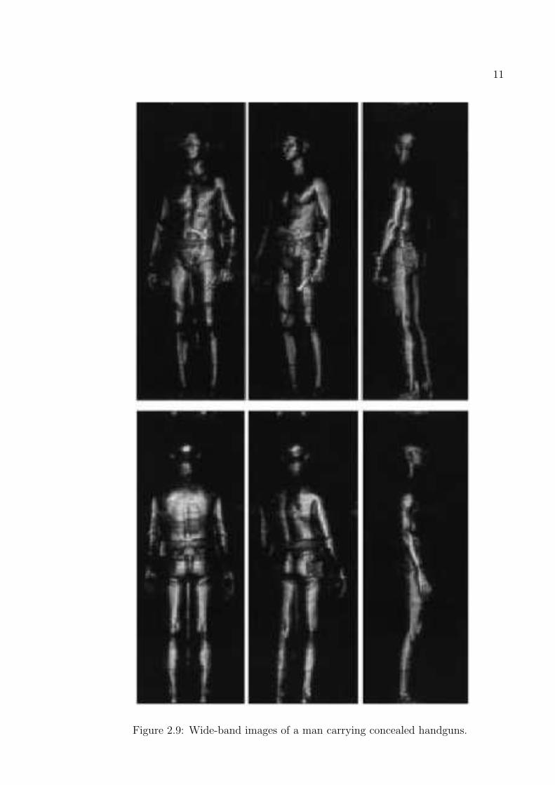
be reconstructed in complete focus. Figure 2.9 shows wide-band (27–33 GHz) images
of a man carrying concealed handguns. The scans take approximately 1 s each and
demonstrate the high image quality compared to that of single frequency systems.
The first image in Figure 2.9 shows a handgun in the man’s beltline. The second
shows a gun in the left-hand pants pocket. The third image shows a vinyl/paper
checkbook in the left-hand pocket. The fifth image shows a leather wallet in the
back right hand pocket. The advantage of these systems over X-Ray systems is that
humans can be safely targeted. However, the millimeter wave systems are based on
visual images that must be scrutinized for legitimate threats.
11
Figure 2.9: Wide-band images of a man carrying concealed handguns.

12
Figure 2.10: Smiths Detection Sentinel II IONSCAN Detection Portal.
2.5 Chemical Trace Detection Systems
Detection of explosives and chemical agents can be detected by ultra-fast gas chro-
matography. The gas chromatograph separates ions accelerated by an electric field
with charged plates [14]. The incoming sample is preconcentrated and injected into
two separate detection systems. One system traps and analyzes the low volatility
compounds such as nitroglycerine, AN, TNT, PETN and RDX. The second system
traps and analyzes high volatile compounds such as EGDN, DMNB, O-MNT and
P-MNT. One such system is the Smith Detection IONSCAN Sentinel II shown in
Figure 2.10. This system directs a person into a portal where air is used to dislodge
particles and vapors trapped on the body and clothing, where they are sampled and
analyzed. Sensitivities of such systems extend down to the picogram level. Non por-
tal based systems that require swiping a sample from electronic devices, documents,
and personal items tend to create traffic bottlenecks, as do metal detection systems.
These systems work well when explosives or chemical agents are located in baggage
or clothing where air can transport enough of the sample to be detected, or if residual
samples remain on personal items. However, carefully placed compounds in electronic
devices may slip right through such detection systems.
While these systems are extremely advanced and capable, there remains a major
13
loophole in our surveillance and detection system infrastructure. Electronic devices
make an appealing transportation medium for explosives and chemical agents. Due to
the densely packed components in a relatively small package, X-Ray and millimeter
wave imaging systems cannot sufficiently analyze internal components. Current secu-
rity measures require security officials to verify functionality of these devices. X-Ray
systems might flag explosive materials located in a suitcase but generally will fail to
detect such materials encased in a metallic enclosure in a spare drive slot in a laptop.
The technology presented in this paper describes a potential strategy for compar-
ing a device and its properties to known signatures for verification and validity of its
composition. Initial work requires various antennas to be characterized and compared
so a determination can be made as to which radiating structure is best suited for this
particular application.

14
Chapter 3
Detection
3.1 Approach
In attempting to measure and analyze the scattering effects of various metallic struc-
tures and electronic devices, the characteristics of the antennas and the device-field
interactions must be understood. Measuring such small backscattered power requires
high directivity antennas, sufficient transmit power, a high dynamic range receiver
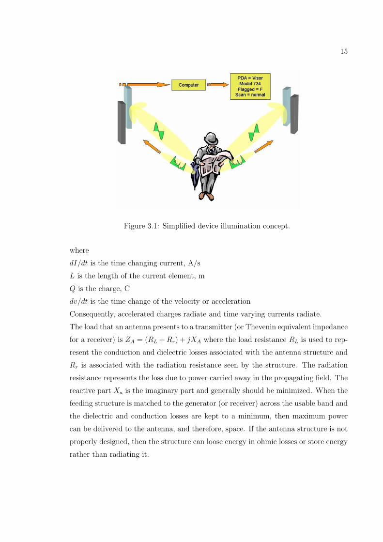
and suppression of multipath and interference. A simplified diagram of the EM illu-
mination concept is presented in Figure 3.1. Section 3.2 describes the theory and
quantifying characteristics of various types of antenna structures.
3.2 Antenna Parameters
The antenna is a transitional structure between free space and a guiding device. It is
used as a transducer that interfaces a circuit and space by transducing an electronic
signal to a propagating electromagnetic signal. The radiation produced by any an-
tenna is provided by the acceleration or deceleration of charge and is described by
the basic radiation equation.
dI
dtL = Q
dv
dt(Am/s) (3.1)
15
Figure 3.1: Simplified device illumination concept.
where
dI/dt is the time changing current, A/s
L is the length of the current element, m
Q is the charge, C
dv/dt is the time change of the velocity or acceleration
Consequently, accelerated charges radiate and time varying currents radiate.
The load that an antenna presents to a transmitter (or Thevenin equivalent impedance
for a receiver) is ZA = (RL + Rr) + jXA where the load resistance RL is used to rep-
resent the conduction and dielectric losses associated with the antenna structure and
Rr is associated with the radiation resistance seen by the structure. The radiation
resistance represents the loss due to power carried away in the propagating field. The
reactive part Xa is the imaginary part and generally should be minimized. When the
feeding structure is matched to the generator (or receiver) across the usable band and
the dielectric and conduction losses are kept to a minimum, then maximum power
can be delivered to the antenna, and therefore, space. If the antenna structure is not
properly designed, then the structure can loose energy in ohmic losses or store energy
rather than radiating it.
16
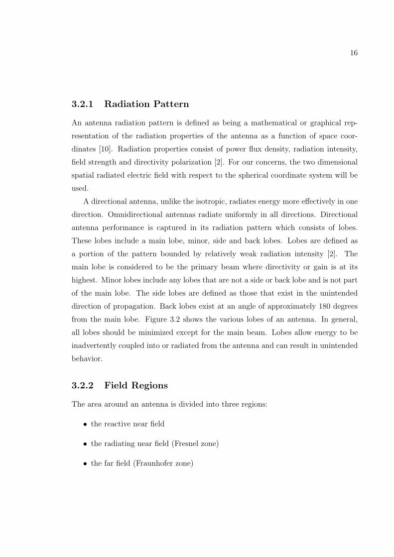
3.2.1 Radiation Pattern
An antenna radiation pattern is defined as being a mathematical or graphical rep-
resentation of the radiation properties of the antenna as a function of space coor-
dinates [10]. Radiation properties consist of power flux density, radiation intensity,
field strength and directivity polarization [2]. For our concerns, the two dimensional
spatial radiated electric field with respect to the spherical coordinate system will be
used.
A directional antenna, unlike the isotropic, radiates energy more effectively in one
direction. Omnidirectional antennas radiate uniformly in all directions. Directional
antenna performance is captured in its radiation pattern which consists of lobes.
These lobes include a main lobe, minor, side and back lobes. Lobes are defined as
a portion of the pattern bounded by relatively weak radiation intensity [2]. The
main lobe is considered to be the primary beam where directivity or gain is at its
highest. Minor lobes include any lobes that are not a side or back lobe and is not part
of the main lobe. The side lobes are defined as those that exist in the unintended
direction of propagation. Back lobes exist at an angle of approximately 180 degrees
from the main lobe. Figure 3.2 shows the various lobes of an antenna. In general,
all lobes should be minimized except for the main beam. Lobes allow energy to be
inadvertently coupled into or radiated from the antenna and can result in unintended
behavior.
3.2.2 Field Regions
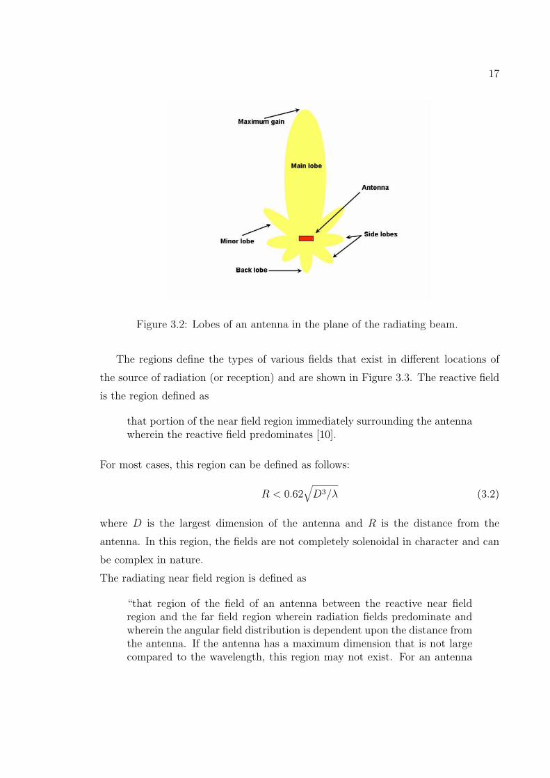
The area around an antenna is divided into three regions:
• the reactive near field
• the radiating near field (Fresnel zone)
• the far field (Fraunhofer zone)
17
Figure 3.2: Lobes of an antenna in the plane of the radiating beam.
The regions define the types of various fields that exist in different locations of
the source of radiation (or reception) and are shown in Figure 3.3. The reactive field
is the region defined as
that portion of the near field region immediately surrounding the antennawherein the reactive field predominates [10].
For most cases, this region can be defined as follows:
R < 0.62√
D3/λ (3.2)
where D is the largest dimension of the antenna and R is the distance from the
antenna. In this region, the fields are not completely solenoidal in character and can
be complex in nature.
The radiating near field region is defined as
“that region of the field of an antenna between the reactive near fieldregion and the far field region wherein radiation fields predominate andwherein the angular field distribution is dependent upon the distance fromthe antenna. If the antenna has a maximum dimension that is not largecompared to the wavelength, this region may not exist. For an antenna

18
Figure 3.3: Various field regions of an antenna.
focused at infinity, the radiating near field region is sometimes referred toas the Fresnel region on the basis of analogy to optical terminology. If theantenna has a maximum overall dimension which is very small comparedto the wavelength, the Fresnel region may not exist [10].”
The boundary for this region can be expressed as follows
0.62√
D3/λ ≤ R < 2D2/λ (3.3)
This criterion is based on a maximum phase error of π/8.
The far field region is defined as
that region of the field of an antenna where the angular field distributionis essentially independent of the distance from the antenna. If the antennahas a maximum overall dimension D, the far field region is commonly takento exist at distances greater than 2D2/λ from the antenna. The far fieldpatterns of certain antennas, such as multibeam reflector antennas, aresensitive to variations in phase over their apertures. For these antennas,2D2/λ may be inadequate. For an antenna focused at infinity, the far fieldregion is sometimes referred to as the Fraunhofer region on the basis ofanalogy to optical terminology [10].
In this region, the fields can be considered transverse and uniform.

19
3.2.3 Directivity, Gain and Antenna Efficiency
The directivity of an antenna is defined as the ratio of the radiation intensity in a
given direction from the antenna to the radiation intensity averaged over all directions,
where the average radiation intensity is equal to the total power radiated by the
antenna divided by 4π. The directivity is defined as
Dmax =4π ∗ Umax
Prad
(3.4)
where:
Dmax is the maximum directivity (dimensionless)
Umax is the maximum radiation intensity (W/unit solid angle)
Prad =is the total radiated power (W)
For the isotropic source, the directivity is unity.
The gain of an antenna can be defined in various ways depending on the number
and types of losses that are taken into account. The gain of an antenna will always
be less than the directivity because of these losses. Such losses can include ohmic
losses in the antenna, losses due to a radome, power that is lost due to heating of the
antenna and feed mismatches. In most formal definitions of gain, mismatch losses
are not to be incorporated in the gain calculation, but for these purposes, mismatch
losses will be included.
The gain is related to the directivity by the antenna efficiency factor:
G = kD (3.5)
where k is the efficiency factor (0 ≤ k ≤ 1), dimensionless. These losses can be of
various forms and depends on the losses that are included in the gain measurements.
The gain of an antenna may be measured by comparing the power density of the
antenna under test (AUT) with an antenna of known gain, such as a horn antenna
or dipole.
Gain = G =Pmax(AUT)
Pmax(ref. ant.)x G(ref. ant.) (3.6)
20
3.2.4 Bandwidth
For the purposes of this research, antennas with broadband operation are important so
that broadband responses from various targets may be measured without changing the
test configuration. This is the motivation for designing the double ridged horn antenna
described in Section 3.3.3). For broadband antennas, the bandwidth is described in
terms of a ratio of the upper frequency of operation to that of the lower. For example,
a 4:1 bandwidth could describe an antenna with a 1–4 GHz operational range. For
narrow bandwidth designs, bandwidth is expressed as a percentage of the upper minus
the lower frequency divided by the center frequency.
3.2.5 Input Impedance
The input impedance of the antenna should ideally match that of the driving trans-
mission line throughout the band of interest. When the feed is not matched across
this band, then mismatch losses become significant and steal from the radiated en-
ergy. The feed structure is commonly the band limiting component of the broadband
antenna structure. Measurements of the input impedance can be expressed as the
SWR and can be measured very easily across the band of interest using a network
analyzer.
3.3 Antennas of Interest
3.3.1 Standard Gain Horn
The standard gain horn is probably one of the simplest and most widely used antenna
structures of all. The horn is a flared out waveguide and produces a uniform phase
front with a larger aperture than the normal waveguide, thereby providing greater
directivity. The standard horn used in this effort minimizes aperture to free space
discontinuities by using a gradual exponential taper in the flare.
The standard gain horn antenna typically has a cutoff wavelength λc of twice its
broad dimension, 2a. Due to its small bandwidth, the standard gain horn will be
21
used strictly for benchmarking purposes.
The directivity of the horn can be expressed in terms of an effective aperture [1],
D =4πAe
λ2=
4πεapAp
λ2(3.7)
where
Ae is the effective aperture, m2
Ap is the physical aperture, m2
εap is the aperture efficiency or Ae/Ap
For a rectangular horn, Ap = aEaH . aE and aH are the physical dimensions of
the width and height of the aperture, respectively and are assumed that each are
at least 1λ. Aperture efficiency has been experimentally calculated as being 0.6 for
most general horn antennas by Alford [1]. Using εap ' 0.6, the directivity can be
approximated as
D ' 7.5Ap
λ2(3.8)
or
D ' 10log(7.5Ap
λ2) (dBi) (3.9)
or more accurately,
D ' 10log(7.5aEλaHλ) (dBi) (3.10)
3.3.2 Conical Spiral
The Conical Spiral Antenna (CSA) or tapered helix, is a circular polarized antenna
with little directivity and is considered to be a frequency independent structure. The
conical spiral retains the frequency independent properties of the planar spiral while
providing broad-lobed unidirectional circularly polarized radiation off of the small
end of the antenna. The basis of operation of these antennas has been investigated
by Rumsey [11] and is based on two principles: the angle principle and the truncation
principle. The angle principle says that the performance of an antenna that is defined
entirely by angles will be frequency independent. Antennas defined entirely by angles
are infinite in size, so an additional consideration is needed. The truncation principle
22
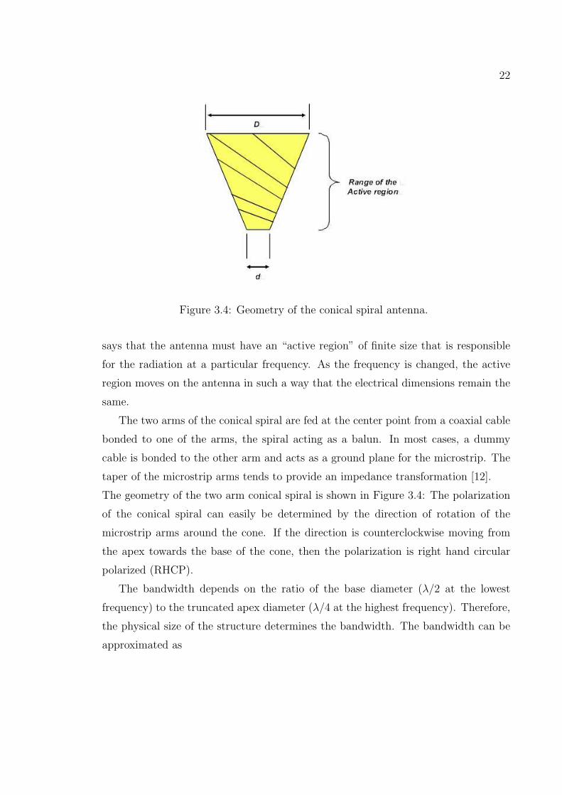
Figure 3.4: Geometry of the conical spiral antenna.
says that the antenna must have an “active region” of finite size that is responsible
for the radiation at a particular frequency. As the frequency is changed, the active
region moves on the antenna in such a way that the electrical dimensions remain the
same.
The two arms of the conical spiral are fed at the center point from a coaxial cable
bonded to one of the arms, the spiral acting as a balun. In most cases, a dummy
cable is bonded to the other arm and acts as a ground plane for the microstrip. The
taper of the microstrip arms tends to provide an impedance transformation [12].
The geometry of the two arm conical spiral is shown in Figure 3.4: The polarization
of the conical spiral can easily be determined by the direction of rotation of the
microstrip arms around the cone. If the direction is counterclockwise moving from
the apex towards the base of the cone, then the polarization is right hand circular
polarized (RHCP).
The bandwidth depends on the ratio of the base diameter (λ/2 at the lowest
frequency) to the truncated apex diameter (λ/4 at the highest frequency). Therefore,
the physical size of the structure determines the bandwidth. The bandwidth can be
approximated as
23
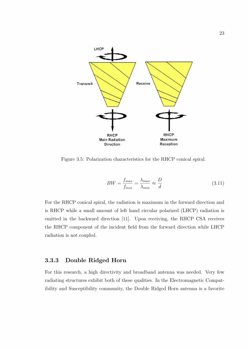
Figure 3.5: Polarization characteristics for the RHCP conical spiral.
BW =fmax
fmin
=λmax
λmin
≈ D
d(3.11)
For the RHCP conical spiral, the radiation is maximum in the forward direction and
is RHCP while a small amount of left hand circular polarized (LHCP) radiation is
emitted in the backward direction [11]. Upon receiving, the RHCP CSA receives
the RHCP component of the incident field from the forward direction while LHCP
radiation is not coupled.
3.3.3 Double Ridged Horn
For this research, a high directivity and broadband antenna was needed. Very few
radiating structures exhibit both of these qualities. In the Electromagnetic Compat-
ibility and Susceptibility community, the Double Ridged Horn antenna is a favorite

24
Figure 3.6: Double ridge horn with coax feed and cross section view.
antenna due to its radiation pattern and high gain. It was determined that designing
a double ridged horn antenna would be best suited for this application.
Adding a double ridge to a waveguide, or horn antenna, lowers the cutoff frequency
because of the capacitive effect at the center of the ridge spacing [3]. In principle,
this cutoff can be lowered substantially by minimizing the ridge spacing, d, sufficiently
which also lowers the input impedance.
The ridges also provide greater separation between modes than do typical waveguide
horn antennas. The general design is shown in Figure 3.6.
The equations for the cutoff wavelengths of the various modes in ridged waveguides
have been derived by Cohen [6] and Walton[7] and are:
B
Dtan θ2 − cot θ1 +
Bc
y01
= 0 (3.12)
B
Dcot θ2 + cot θ1 − Bc
y01
= 0 (3.13)
where
θ1 =360
λc
(A− S
2)degrees (3.14)
θ2 =360
λc
(S
2)degrees (3.15)

25
Figure 3.7: Double ridge horn design curves from Walton [7].
These equations are solved and plotted in Figure 3.7.
The design of the double ridged horn [7] is based on three dimension ratios: s/a,
b/a and d/b. The dimensions chosen for the design used in this research effort are:
• s = 1.9cm (width of ridge)
• a = 5.5cm (inside width of throat)
• b = 1.8cm (inside height of throat)
• d = 0.2cm (spacing between ridges at throat)
Which gives the following ratios:
• s/a = .35
• b/a = .33
• d/b = .11
26
Using the graph in Figure 3.7, this equates to the following cutoff frequencies:
• λcTE10 = 1.09 GHz
• λcTE30 = 10.9 GHz
Thus the antenna is usable over the range 1.09 to 10.9 GHz for a bandwidth of 10:1
or 165%.
The cutoff for λcTE30 is relatively insensitive to changes in d/b, but λcTE10 changes
significantly, where the maximum usable bandwidth increases very rapidly as the gap
becomes smaller.
The design considerations for the ridges were such that a smooth taper transitions
the 50 ohm feed to the impedance of free space. For ease of fabrication, the ridges
were kept at a single width. With a constant ridge width, the overall length of the
horn flare should be as long as possible to allow the impedance transformation to
take place over at least half a wavelength at the lowest operating frequency.
The gap between the actual coaxial feed center conductor and the shorting plate
must be less than one half of a wavelength at the highest frequency. The gap dimen-
sion d for this design is 0.7cm, which accommodates a high cutoff frequency of 21
GHz.
The dimension b must be kept less than a wavelength at the highest operating
frequency to prevent propagation of the TE02 mode. This dimension initially was
9cm, but was changed to 1.8cm with the deflector plates in the throat (see Figure
4.6). These plates were added to suppress higher order modes while keeping the
dimension ratios such that the fundamental mode still propagates. Another critical
dimension ratio is that of s/a. Since the ridge width is dictated by the 1.9cm thickness
of the aluminum sheet used to build them, dimension a has little flexibility. This was
another motivation for the use of the deflector plates. The goal was to try and design
a throat that had dimensions that varied in the direction of propagation, enabling a
broader band of operation.
Final antenna performance results are presented in Chapter 4.
27
3.4 Reflection and Transmission of EM Waves
When an electromagnetic wave propagates through free space and illuminates a sur-
face characterized by µ and ε, energy will be reflected, transmitted or absorbed [5].
For simplicity, we will first consider our targets as perfect electric conducting (PEC)
surfaces with εr = ε′−jσ/ε0ω = ∞ as the conductivity σ, the reciprocal of resistivity,
is infinite. This means that the skin depth will be zero because of the following:
δ = 1/√
fπµσ (3.16)
This implies that the fields inside the conductor are zero and that the electrons re-
spond instantly to an applied electric field. However, because these electrons represent
a charge density, their movement creates their own electric field, which constitutes
the scattered field. These electrons move only when the net electric field is nonzero,
so the field created by the electrons is in the opposite direction to the incident field.
Therefore, when the scattered field is equal and opposite to the incident field, the
total field on the conductor is zero and a net force is no longer acting to move the
electrons. This is due to the boundary condition of a perfectly conducting metal
having zero tangential electric fields.
Since the incident wave is time varying, the equilibrium does not last and the
electrons must move in response to the changing incident field in order to maintain
the zero tangential surface field. The time varying incident field causes a time varying
charge separation on the conductor, in turn creating a current flow. This charge
acceleration and deceleration (or time varying current) is the source for the scattered
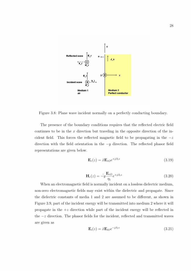
field. Figure 3.8 shows a uniform plane wave propagating in the +z direction in air
and normally incident on a perfect conducting surface at z = 0. The incident wave is
chosen to be in the x direction and therefore the magnetic field is in the y direction.
The incident phasor field representations are given below.
Ei(z) = xEiOe−jβ1z (3.17)
Hi(z) = yEiO
η1
e−jβ1z (3.18)
28
Figure 3.8: Plane wave incident normally on a perfectly conducting boundary.
The presence of the boundary conditions requires that the reflected electric field
continues to be in the x direction but traveling in the opposite direction of the in-
cident field. This forces the reflected magnetic field to be propagating in the −z
direction with the field orientation in the −y direction. The reflected phasor field
representations are given below.
Er(z) = xErOe+jβ1z (3.19)
Hr(z) = −yErO
η1
e+jβ1z (3.20)
When an electromagnetic field is normally incident on a lossless dielectric medium,
non-zero electromagnetic fields may exist within the dielectric and propagate. Since
the dielectric constants of media 1 and 2 are assumed to be different, as shown in
Figure 3.9, part of the incident energy will be transmitted into medium 2 where it will
propagate in the +z direction while part of the incident energy will be reflected in
the −z direction. The phasor fields for the incident, reflected and transmitted waves
are given as
Ei(z) = xEiOe−jβ1z (3.21)

29
Figure 3.9: Plane wave incident normally on a lossless dielectric boundary.
Hi(z) = yEiO
η1
e−jβ1z (3.22)
Er(z) = xErOe+jβ1z (3.23)
Hr(z) = −yErO
η1
e+jβ1z (3.24)
Et(z) = xEtOe−jβ1z (3.25)
Ht(z) = yEtO
η1
e−jβ1z (3.26)
These principles may be expanded into multiple dielectric boundaries with various
angles of incidence to analyze the phenomena taking place with device illumination.
Although this analysis is applicable only for simple boundary problems, advanced
numerical method simulators can be used for more complicated illumination scenarios.
30
3.5 Network Analyzer Calibration
For most measurements, a normal short, open, load and through (SOLT) calibration
procedure was used. The calibration reference plane was set at the antenna connector
and not at the ideal location of the aperture of the antenna. Another calibration
method that proved quite useful was simply subtracting the environment (including
the target mount) from each measurement. The Agilent 8510C math feature was
used to subtract the empty environment trace from the actual data trace. Although
no phase information was preserved, the magnitude measurements are accurate and
are very sensitive to small variations in the received field.
3.6 Summary
Electromagnetic illumination requires that high directivity antennas are utilized with
sufficient radiating properties. In this chapter, the foundations for antenna charac-
terization have been established as it applies to the research presented here. Further-
more, the theory behind the double ridged horn antenna has been examined. The
basics of electromagnetic waves incident on metallic and lossless dielectric boundaries
have been established. A brief discussion of network analyzer calibration procedures
appropriate for this application has been presented.
31
Chapter 4
Antenna Characterization Results
4.1 Time Gating
The time gating feature of the Agilent 8510C Vector Network Analyzer (VNA) pro-
vided a means for gating out unwanted reflections from the test environment. Because
an anechoic chamber was not readily available for the antenna characterization, it is
shown that this type of gating improves measurement results.
The method used is as follows. The 8510C is calibrated using a standard SOLT
calibration up to the feed of the antenna. Depending on the antenna and the number
of adapters that cannot be included into the calibration (and the length of feed
cable), the port extension feature is used to “dial out” the extra adaptors or cables.
The transmit antenna is setup to radiate out into free space. A metallic reflector is
placed at a known distance in the main beam of the transmit antenna. The measured
distance is subtracted from the known distance, multiplied by two and divided by
the speed of light. The resulting time value, which is typically several nanoseconds,
is then entered into the network analyzer to accommodate for the electrical length.
Figure 4.1 shows the test configuration for time gating calibration. This calibrates the
range for any type of unknown cable lengths, adaptors, feeds, etc. Once the antenna
range dimensions agree with the distance (or time) reported by the VNA, accurate
time gating can be utilized. Figure 4.2 demonstrates the effect of the peaks created
by a metal sheet (at 20 ns), a metallic table leg (at 13 ns) and a target of microstrips

32
Figure 4.1: Time gating calibration configuration.
(at 4 ns). Once it is determined which peak is associated with the target of interest,
clutter reflections can easily be time-gated. This procedure has been used in the
majority of the remaining measurements to create essentially a spatially filtered test
range.
4.2 Standing Wave Ratio
The standing wave ratio (SWR) is defined as a measure of mismatch in a line and
ranges from 1 to ∞, 1 being a perfect impedance match. The SWR can be defined as
SWR =Vmax
Vmin
=1 + |Γ|1− |Γ| (4.1)
4.2.1 Standard Gain Horn Antenna
The SWR for a Narda standard gain horn (model 642) is shown in Figure 4.3 and dis-
plays the usable bandwidth of the antenna as being between 5.3–8.2 GHz. Although
the SWR is flat for this band, it is clear that this antenna will not be of much interest
due to its lack of bandwidth. However, it provides a nice reference for the remaining

33
0 5 10 15 20 25 300
0.5
1
1.5
2
2.5
3
3.5x 10
−3
time (ns)
S21
(lin
ear)
Time domain with and without microstrip target
with microstrip without microstrip
Figure 4.2: Time domain analysis of target with clutter.
4 6 8 10 12 14 16 18 200
1
2
3
4
5
6
7
8
9
10
freq (GHz)
SW
R
SWR of the Narda 5.3 − 8.2 GHz horn
Narda horn
Figure 4.3: SWR of Narda (model 642) 5.3–8.2 GHz standard gain horn antenna.

34
Figure 4.4: Conical spiral RHCP antenna.
0 2 4 6 8 10 12 14 16 18 200
1
2
3
4
5
6
7
8
9
10
freq (GHz)
SW
R
SWR of the conical spiral
conical spiral
Figure 4.5: SWR of conical spiral antenna.
measurements.
4.2.2 Conical Spiral Antenna
The conical spiral antenna has attractive features such as an SWR average of approx-
imately 2 and a bandwidth of greater than 6:1. The disadvantage of this structure
is the broad beamwidth and low directivity. A picture of the RHCP conical spiral
antenna is shown in Figure 4.4. The SWR is relatively flat from 2–16 GHz except
for a major peak at approximately 10.5 GHz and is shown in Figure 4.5. Although

35
Figure 4.6: Double ridged horn antenna.
the SWR remains under 2 up to 16 GHz, the actual band of operation has an upper
frequency limit of approximately 10 GHz, (as discussed in Section 4.4.2) due to large
variations in it’s transmitted response.
4.2.3 Double Ridged Horn Antenna
The double ridged horn antenna is shown in Figure 4.6. In the second picture, the
deflector plates can easily be seen inside of the throat area. The overall dimensions
of the antennas are:
Width of aperture = 35.7 cm
Height of aperture = 27.5 cm
Overall length, including throat assembly = 52 cm
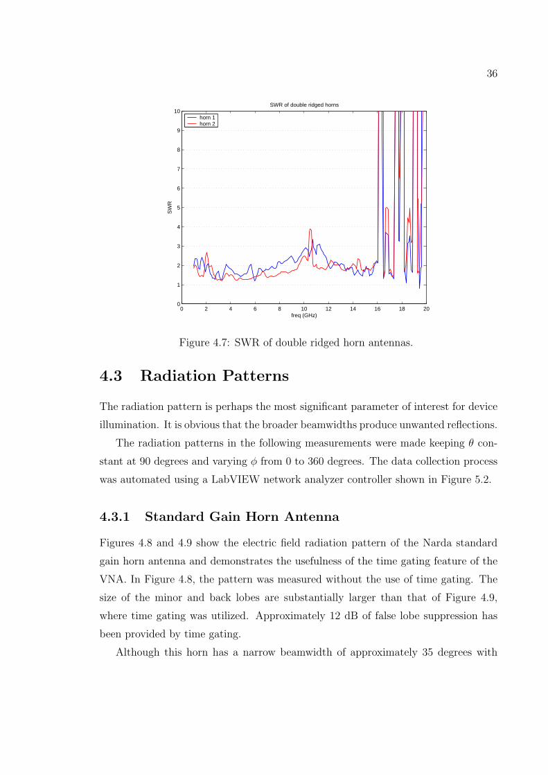
The SWR measurements of each of the double ridged horn antennas are shown in
Figure 4.7. Each antenna exhibits a unique SWR response with an average value of
approximately 2. This equates to a reflection coefficient of 0.33 and a return loss of 9.5
dB. The antennas have a relatively consistent SWR envelope but display independent
deficiencies across the band. Horn 1 has approximately 4.5 dB more return loss in
the 7–9 GHz band compared to that of horn 2. Horn 2 has a peak in the SWR at 2
GHz of approximately 2.8, which equates to 6.4 dB of return loss.
Matching improvements in the feed structures could drastically improve the overall
performance of these antennas.
36
0 2 4 6 8 10 12 14 16 18 200
1
2
3
4
5
6
7
8
9
10
freq (GHz)
SW
R
SWR of double ridged horns
horn 1horn 2
Figure 4.7: SWR of double ridged horn antennas.
4.3 Radiation Patterns
The radiation pattern is perhaps the most significant parameter of interest for device
illumination. It is obvious that the broader beamwidths produce unwanted reflections.
The radiation patterns in the following measurements were made keeping θ con-
stant at 90 degrees and varying φ from 0 to 360 degrees. The data collection process
was automated using a LabVIEW network analyzer controller shown in Figure 5.2.
4.3.1 Standard Gain Horn Antenna
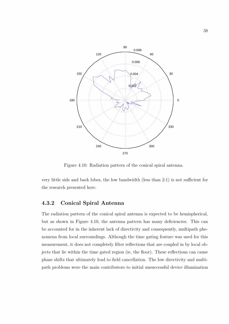
Figures 4.8 and 4.9 show the electric field radiation pattern of the Narda standard
gain horn antenna and demonstrates the usefulness of the time gating feature of the
VNA. In Figure 4.8, the pattern was measured without the use of time gating. The
size of the minor and back lobes are substantially larger than that of Figure 4.9,
where time gating was utilized. Approximately 12 dB of false lobe suppression has
been provided by time gating.
Although this horn has a narrow beamwidth of approximately 35 degrees with
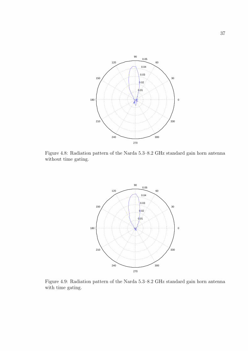
37
0.01
0.02
0.03
0.04
0.05
30
210
60
240
90
270
120
300
150
330
180 0
Figure 4.8: Radiation pattern of the Narda 5.3–8.2 GHz standard gain horn antennawithout time gating.
0.01
0.02
0.03
0.04
0.05
30
210
60
240
90
270
120
300
150
330
180 0
Figure 4.9: Radiation pattern of the Narda 5.3–8.2 GHz standard gain horn antennawith time gating.
38
0.002
0.004
0.006
0.008
30
210
60
240
90
270
120
300
150
330
180 0
Figure 4.10: Radiation pattern of the conical spiral antenna.
very little side and back lobes, the low bandwidth (less than 2:1) is not sufficient for
the research presented here.
4.3.2 Conical Spiral Antenna
The radiation pattern of the conical spiral antenna is expected to be hemispherical,
but as shown in Figure 4.10, the antenna pattern has many deficiencies. This can
be accounted for in the inherent lack of directivity and consequently, multipath phe-
nomena from local surroundings. Although the time gating feature was used for this
measurement, it does not completely filter reflections that are coupled in by local ob-
jects that lie within the time gated region (ie, the floor). These reflections can cause
phase shifts that ultimately lead to field cancellation. The low directivity and multi-
path problems were the main contributors to initial unsuccessful device illumination
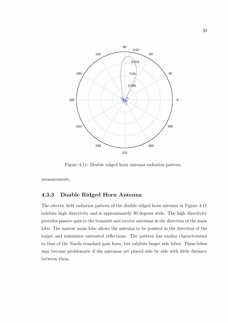
39
0.005
0.01
0.015
0.02
30
210
60
240
90
270
120
300
150
330
180 0
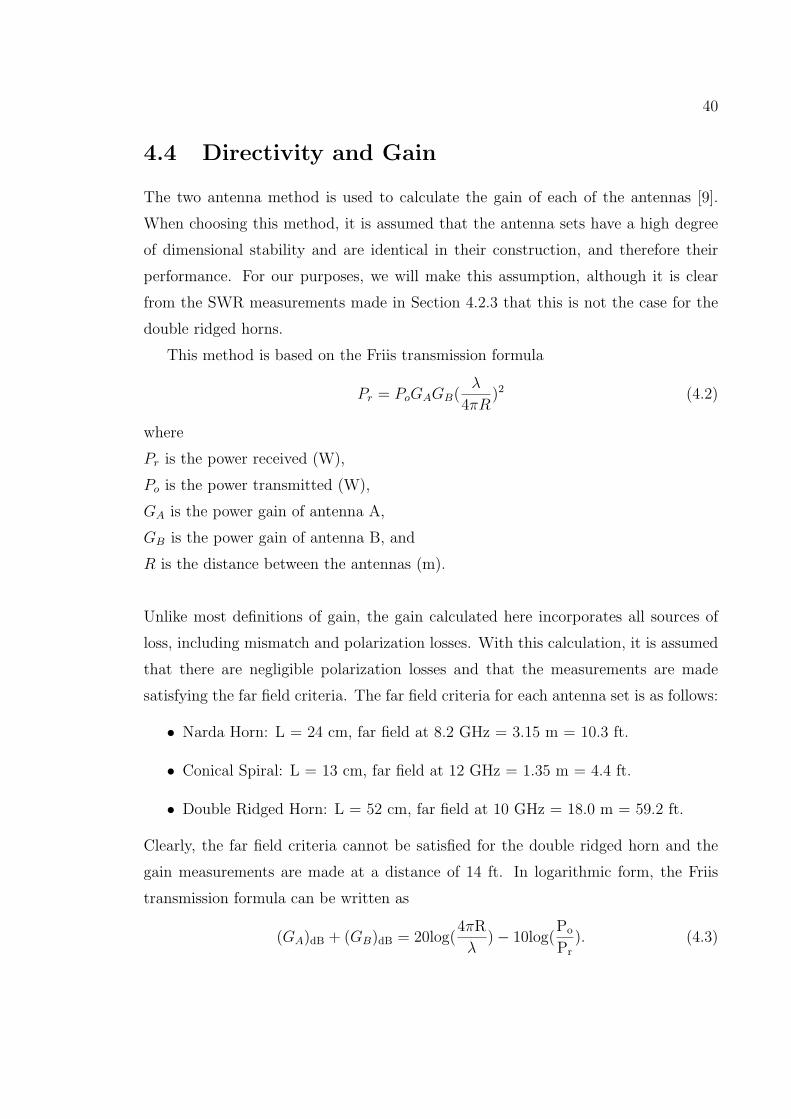
Figure 4.11: Double ridged horn antenna radiation pattern.
measurements.
4.3.3 Double Ridged Horn Antenna
The electric field radiation pattern of the double ridged horn antenna in Figure 4.11
exhibits high directivity and is approximately 30 degrees wide. The high directivity
provides passive gain to the transmit and receive antennas in the direction of the main
lobe. The narrow main lobe allows the antenna to be pointed in the direction of the
target and minimizes unwanted reflections. The pattern has similar characteristics
to that of the Narda standard gain horn, but exhibits larger side lobes. These lobes
may become problematic if the antennas are placed side by side with little distance
between them.
40
4.4 Directivity and Gain
The two antenna method is used to calculate the gain of each of the antennas [9].
When choosing this method, it is assumed that the antenna sets have a high degree
of dimensional stability and are identical in their construction, and therefore their
performance. For our purposes, we will make this assumption, although it is clear
from the SWR measurements made in Section 4.2.3 that this is not the case for the
double ridged horns.
This method is based on the Friis transmission formula
Pr = PoGAGB(λ
4πR)2 (4.2)
where
Pr is the power received (W),
Po is the power transmitted (W),
GA is the power gain of antenna A,
GB is the power gain of antenna B, and
R is the distance between the antennas (m).
Unlike most definitions of gain, the gain calculated here incorporates all sources of
loss, including mismatch and polarization losses. With this calculation, it is assumed
that there are negligible polarization losses and that the measurements are made
satisfying the far field criteria. The far field criteria for each antenna set is as follows:
• Narda Horn: L = 24 cm, far field at 8.2 GHz = 3.15 m = 10.3 ft.
• Conical Spiral: L = 13 cm, far field at 12 GHz = 1.35 m = 4.4 ft.
• Double Ridged Horn: L = 52 cm, far field at 10 GHz = 18.0 m = 59.2 ft.
Clearly, the far field criteria cannot be satisfied for the double ridged horn and the
gain measurements are made at a distance of 14 ft. In logarithmic form, the Friis
transmission formula can be written as
(GA)dB + (GB)dB = 20log(4πR
λ)− 10log(
Po
Pr
). (4.3)
41
5 5.5 6 6.5 7 7.5 8 8.513
13.5
14
14.5
15
15.5
16
16.5
17
17.5
Frequency (GHz)
dBi
Directivity and Gain of the Narda Horn
Gain Directivity
Figure 4.12: Calculated directivity and measured gain of the Narda standard horn.
Based on the assumption that the antennas have identical gains, then equation 4.3
can be written as
(GA)dB = (GB)dB =1
2[20log(
4πR
λ)− 10log(
Po
Pr
)]. (4.4)
This equation is used in the next few sections to calculate the gain of the antennas
across their band of operation. This is accomplished by making an S21 measurement
across the band for a given antenna set. S21 is squared to give a power ratio and
used in Equation 4.4.
4.4.1 Standard Gain Horn Antenna
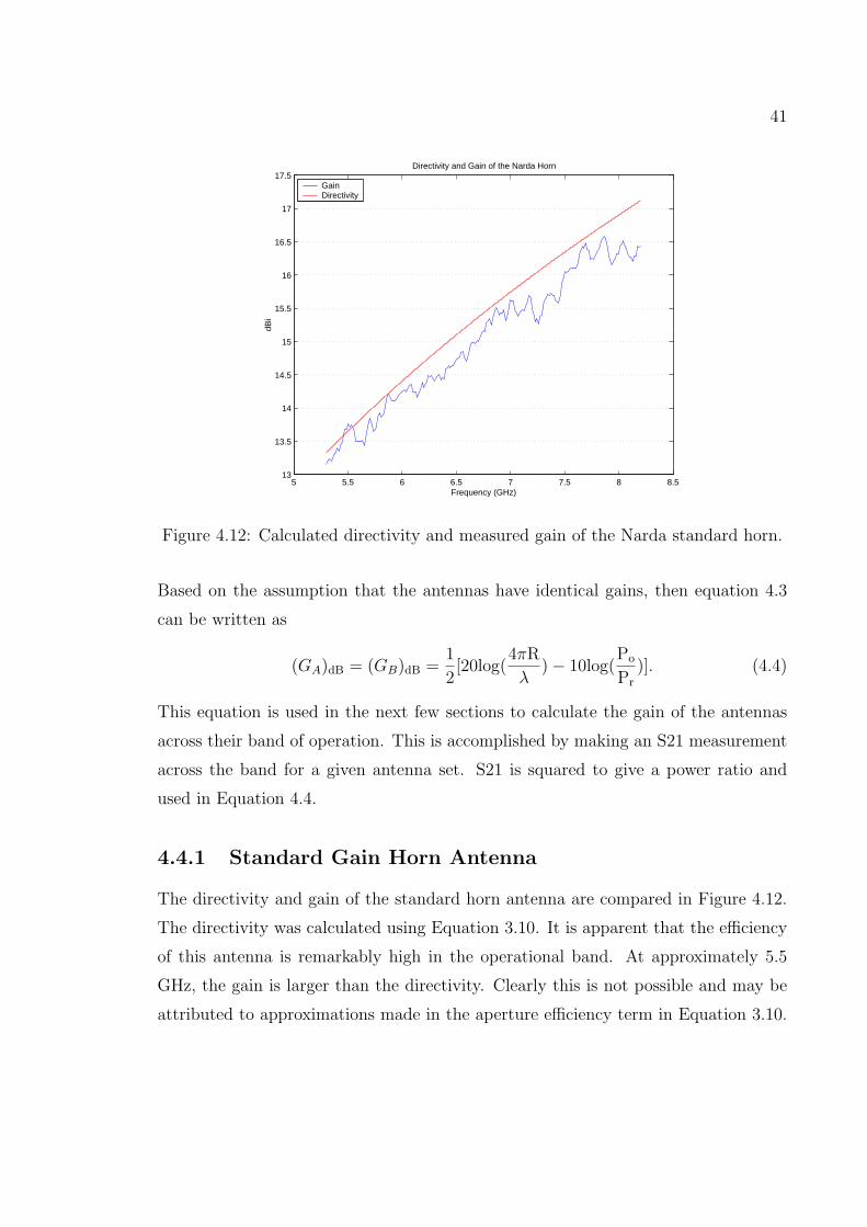
The directivity and gain of the standard horn antenna are compared in Figure 4.12.
The directivity was calculated using Equation 3.10. It is apparent that the efficiency
of this antenna is remarkably high in the operational band. At approximately 5.5
GHz, the gain is larger than the directivity. Clearly this is not possible and may be
attributed to approximations made in the aperture efficiency term in Equation 3.10.

42
0 2 4 6 8 10 12 14 16−25
−20
−15
−10
−5
0
5
10
Frequency (GHz)
Ant
enna
Gai
n
Gain of Conical Spiral
Conical Spiral
Figure 4.13: Gain of the conical spiral antenna.
A value of 0.6 was used, but the aperture efficiency of these particular horns might
be higher since they have an exponential taper.
4.4.2 Conical Spiral Antenna
The gain of the conical spiral antenna is shown in Figure 4.13. A directivity calcula-
tion was not attempted for this structure. From the gain, the operational bandwidth
appears to be between 2 and 10 GHz. It is clear from Figure 4.13 that there are wide
variations in the antenna response. Considering the radiation plot in Figure 4.10 and
the SWR plot in Figure 4.5, deviations in the response could be attributed to reflec-
tions internal to the conical spiral feed or balun. The fluctuations in the passband
gain above 6 GHz reach 10 dB and more.
4.4.3 Double Ridged Horn Antenna
The directivity and gain of the double ridged horn antenna are shown in Figure 4.14.
The efficiency of these antennas are clearly lacking in portions of the band, especially
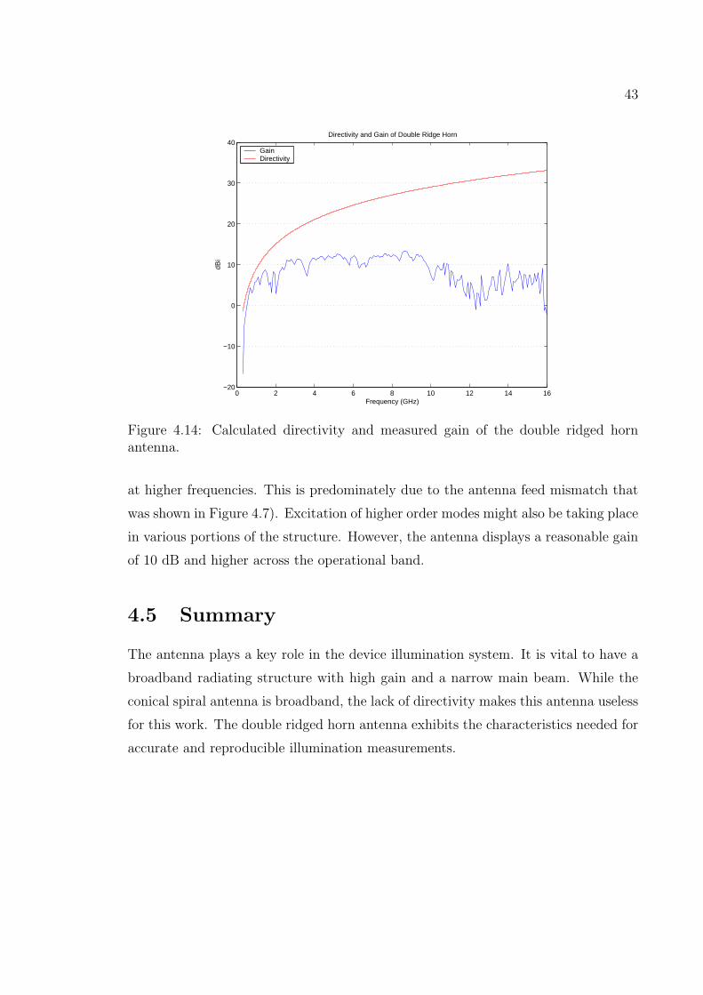
43
0 2 4 6 8 10 12 14 16−20
−10
0
10
20
30
40
Frequency (GHz)
dBi
Directivity and Gain of Double Ridge Horn
Gain Directivity
Figure 4.14: Calculated directivity and measured gain of the double ridged hornantenna.
at higher frequencies. This is predominately due to the antenna feed mismatch that
was shown in Figure 4.7). Excitation of higher order modes might also be taking place
in various portions of the structure. However, the antenna displays a reasonable gain
of 10 dB and higher across the operational band.
4.5 Summary
The antenna plays a key role in the device illumination system. It is vital to have a
broadband radiating structure with high gain and a narrow main beam. While the
conical spiral antenna is broadband, the lack of directivity makes this antenna useless
for this work. The double ridged horn antenna exhibits the characteristics needed for
accurate and reproducible illumination measurements.

44
Chapter 5
Device Illumination Results
There are very distinct signatures of simple and complex passive and electronic de-
vices. The test environment and radiating equipment plays a key role in obtaining
meaningful, reproducible and accurate results. The ability to time-gate out unwanted
reflections and multipath residues greatly enhances accuracy of results when an ane-
choic chamber or an antenna test range is not available.
5.1 Illumination of Various Structures
5.1.1 Test Configuration
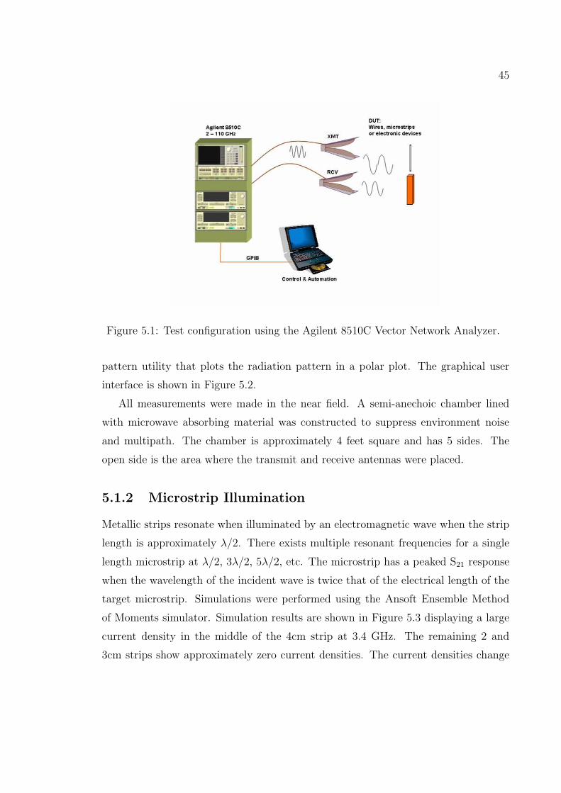
The test configuration used for measuring the backscattered power from various tar-
gets is shown in Figure 5.1. The transmit antenna is connected to test port 1 of the
network analyzer and the receive antenna is connected to test port 2. All measure-
ments were made in terms of S21 and it was assumed that the ports were matched
over the frequency band of the measurement. This implies that V −1 and V +
2 are zero
and that no power is lost due to mismatch and discontinuities in the connections.
The Agilent 8510 network analyzer has a system dynamic range of 93 dB and
has convenient features for suppressing noise such as data averaging, trace math and
trace smoothing. A LabVIEW control system was designed to collect, parse and plot
data in a variety of formats. The control system encompasses an antenna radiation
45
Figure 5.1: Test configuration using the Agilent 8510C Vector Network Analyzer.
pattern utility that plots the radiation pattern in a polar plot. The graphical user
interface is shown in Figure 5.2.
All measurements were made in the near field. A semi-anechoic chamber lined
with microwave absorbing material was constructed to suppress environment noise
and multipath. The chamber is approximately 4 feet square and has 5 sides. The
open side is the area where the transmit and receive antennas were placed.
5.1.2 Microstrip Illumination
Metallic strips resonate when illuminated by an electromagnetic wave when the strip
length is approximately λ/2. There exists multiple resonant frequencies for a single
length microstrip at λ/2, 3λ/2, 5λ/2, etc. The microstrip has a peaked S21 response
when the wavelength of the incident wave is twice that of the electrical length of the
target microstrip. Simulations were performed using the Ansoft Ensemble Method
of Moments simulator. Simulation results are shown in Figure 5.3 displaying a large
current density in the middle of the 4cm strip at 3.4 GHz. The remaining 2 and
3cm strips show approximately zero current densities. The current densities change

46
Figure 5.2: LabVIEW control system for the Agilent 8510C Vector Network Analyzer.
Figure 5.3: Current density at 3.4 GHz for a 4cm strip illuminated by a plane wave

47
from each of the strips as the incident wave frequency increases and reaches twice the
electrical length of the other strips.
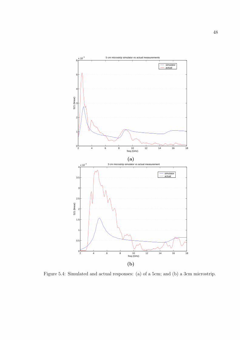
In Figure 5.4, the measured and simulated response of a 5cm and 3cm long mi-
crostrip are shown. For the 5cm strip, there is agreement at the first resonance of
approximately 3 GHz (λ/2) and at the second resonance of approximately 9 GHz
(3λ/2). For the 3cm strip, there is agreement at the first resonance at approximately
5 GHz (λ/2) and at the second resonance of approximately 16 GHz (3λ/2). As the
strip length becomes shorter and the width remains unchanged, the resonant fre-
quency increases and the peak becomes more broad. The broadband nature of the
response is caused by the increase in the surface resistance with increasing frequency,
resulting in a decrease in the microstrip Q. The lower Q results in a higher bandwidth
response.
The discrepancies in magnitude are due to errors in converting from the simulated
radar cross section (RCS) to S21. The simulator results are in terms of RCS (σ) which
is defined as follows.
σ = 4πR2Pscattered
Pincident
(5.1)
RCS is defined at the target and the measured S21 is defined at the calibration plane
of the antennas. Therefore the conversion process must incorporate the difference in
distance and is merely an estimate.
The resonating frequency of a microstrip decreases slightly as the width of the
microstrip increases. As the geometry approaches a square, the induced current on
the strip begins to travel between diagonal corners as well as opposing ends. This
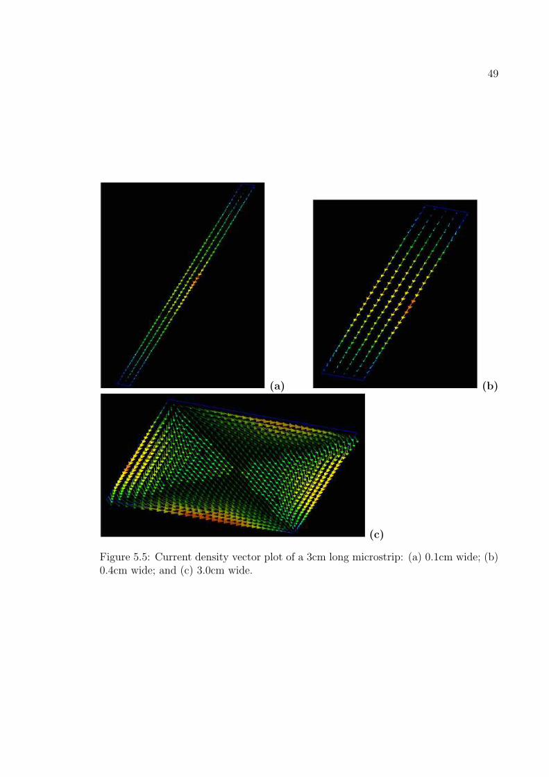
phenomena is shown in Figure 5.5. It is not until the width becomes close to the
length, that a transverse resonance begins to appear. Transverse resonance occurs
only when the incident wave contains both a horizontal and a vertical component.
Figure 5.6 shows the simulated and the measured response of a 3cm long microstrip
of various widths.
As the strip becomes wider and approaches a square, the response begins to
broaden out and the resonant peak disappears. The response becomes high pass
in nature. Specular reflections become the dominating mechanism as the wavelength
48
2 4 6 8 10 12 14 16 180
1
2
3
4
5
6x 10
−3
freq (GHz)
S21
(lin
ear)
5 cm microstrip simulator vs actual measurements
simulatoractual
(a)
2 4 6 8 10 12 14 16 180
0.5
1
1.5
2
2.5
3
3.5
4x 10
−3
freq (GHz)
S21
(lin
ear)
3 cm microstrip simulator vs actual measurement
simulatoractual
(b)
Figure 5.4: Simulated and actual responses: (a) of a 5cm; and (b) a 3cm microstrip.
49
(a) (b)
(c)
Figure 5.5: Current density vector plot of a 3cm long microstrip: (a) 0.1cm wide; (b)0.4cm wide; and (c) 3.0cm wide.

50
2 4 6 8 10 12 14 16 180
0.2
0.4
0.6
0.8
1
1.2
1.4
1.6
1.8x 10
−3
freq (GHz)
S21
(lin
ear)
S21 response of various width 3 cm microstrip
0.1 cm wide0.4 cm wide0.9 cm wide
(a)
2 4 6 8 10 12 14 16 180
0.5
1
1.5
2
2.5
3
3.5
4
4.5x 10
−3 Plot of the RCS of a 3 cm long microstrip of various widths
frequency (GHz)
RC
S (
dBm
)
0.1 cm wide0.4 cm wide0.9 cm wide
(b)
Figure 5.6: Simulated (a) and actual (b) response of a 3cm long microstrip of variouswidths.

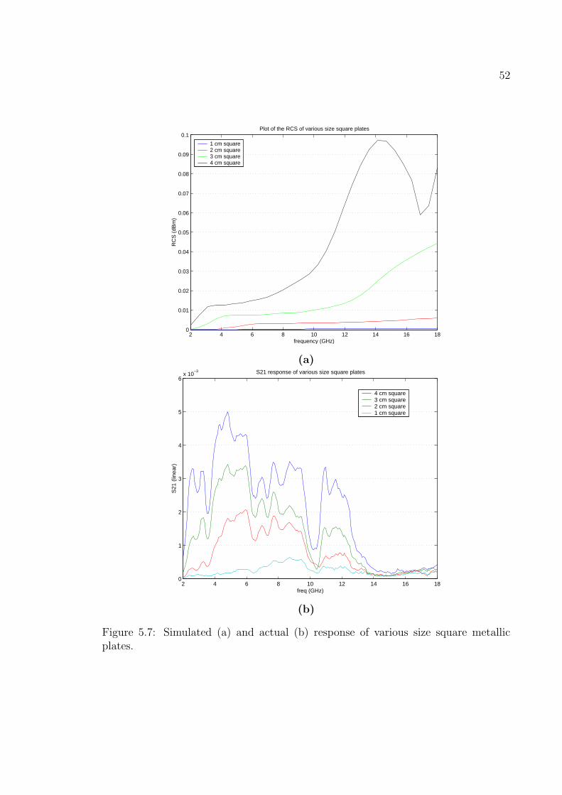
51
becomes smaller than the electrical size of the square. This is shown in the simulated
results in Figures 5.7 and 5.8.
A square plate begins to reflect high frequencies in a specular fashion as the
wavelength becomes smaller than the electrical size. There is substantial disagreement
between the actual and simulated response for square conducting plates. This is
attributed to the antenna response deficiencies at the higher frequencies.
Multiple microstrips on a single target respond in the same fashion as do the
individual strips. Linear superposition appears to hold only when sufficient spacing
is placed between the strips. This distance has been experimentally determined as
approximately λ/2. Complex field interactions begin to dominate when the spacing
becomes smaller. As the spacing continues to decrease, it responds as if the strips were
a single metallic entity. This is shown in Figures 5.9 and 5.10. The inconsistencies
between actual and simulated results may be due to the limitations of the simulator
used. The simulator requires that targets be placed on an air box that is not quite
large enough to allow sufficient λ/2 spacing between the air box boundaries and the
neighboring strips.
A summary of the various microstrip length responses are shown in Figure 5.11.
The lengths range from 1cm to 6cm in 0.2cm increments. The second resonances at
3λ/2 begin to appear for the lengths starting at approximately 4cm.
5.1.3 Laptop Illumination
Unique signatures exist for each of the laptops illuminated. Each laptop exhibits
peaks in different portions of the frequency spectrum. The magnitude of these peaks
change as various components and drives are removed. It appears as if various mech-
anisms are contributing to the responses of compact electronic devices. Resonant
behavior occurs for metallic traces that are aligned with the polarization of the in-
cident field and have sufficient spacing with other scatterers. Specular reflections
occur for metallic interfaces that are electrically larger than the incident wavelength.
Dielectric boundaries will reflect electromagnetic energy and reflections depend on
frequency, material properties and losses.
52
2 4 6 8 10 12 14 16 180
0.01
0.02
0.03
0.04
0.05
0.06
0.07
0.08
0.09
0.1Plot of the RCS of various size square plates
frequency (GHz)
RC
S (
dBm
)
1 cm square2 cm square3 cm square4 cm square
(a)
2 4 6 8 10 12 14 16 180
1
2
3
4
5
6x 10
−3
freq (GHz)
S21
(lin
ear)
S21 response of various size square plates
4 cm square3 cm square2 cm square1 cm square
(b)
Figure 5.7: Simulated (a) and actual (b) response of various size square metallicplates.

53
00.5
11.5
22.5
3
0
2
4
6
8
100
0.002
0.004
0.006
0.008
0.01
width in cm
Strip width vs Frequency vs RCS
freq (GHz)
RC
S
Figure 5.8: Radar cross section (RCS) simulation results for a 3cm microstrip withwidths varying from 0.1cm to 3.0cm.

54
2 3 4 5 6 7 8 9 10 11 120
0.5
1
1.5
2
2.5
3
3.5
4x 10
−3
freq (GHz)
S21
(lin
ear)
Multiple length microstrips
simulatoractual
Figure 5.9: Simulated and actual results for 4, 3, and 2cm microstrips.
2 4 6 8 10 12 14 16 180
0.5
1
1.5
2
2.5
3
3.5
4
4.5
5x 10
−3
freq (GHz)
S21
(lin
ear)
Multiple length microstrips
all strips1 cm 2 cm 3 cm 4 cm
Figure 5.10: Single and multiple S21 strip response demonstrating linear superposi-tion.

55
0
10
20
30
0.20.40.60.811.21.41.61.8x 10
10
0
1
2
3
4
5
6
x 10−3
frequency (Hz)
Strip length (1cm − 6cm)
S21
Figure 5.11: Actual S21 response of various length microstrips ranging in length from1.0 to 6.0 cm.
56
2 3 4 5 6 7 80
0.002
0.004
0.006
0.008
0.01
0.012
freq (GHz)
S21
(lin
ear)
S21 of NEC and Winbook laptops
NEC Winbook
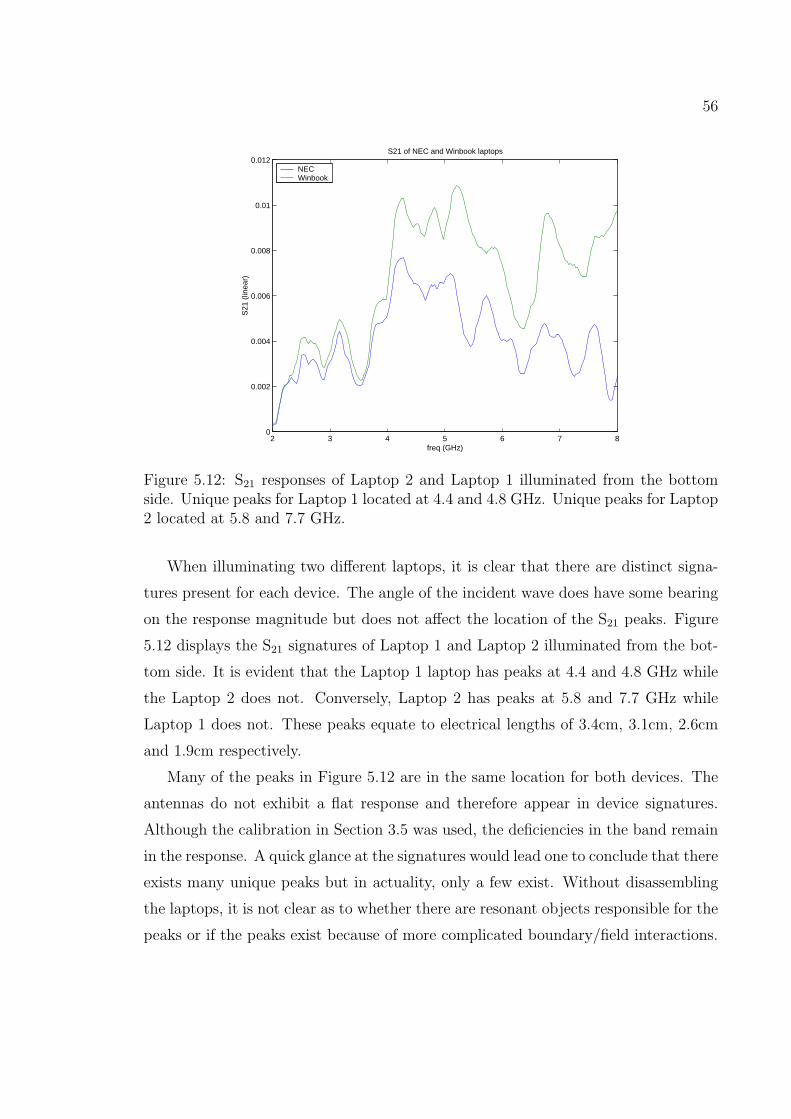
Figure 5.12: S21 responses of Laptop 2 and Laptop 1 illuminated from the bottomside. Unique peaks for Laptop 1 located at 4.4 and 4.8 GHz. Unique peaks for Laptop2 located at 5.8 and 7.7 GHz.
When illuminating two different laptops, it is clear that there are distinct signa-
tures present for each device. The angle of the incident wave does have some bearing
on the response magnitude but does not affect the location of the S21 peaks. Figure
5.12 displays the S21 signatures of Laptop 1 and Laptop 2 illuminated from the bot-
tom side. It is evident that the Laptop 1 laptop has peaks at 4.4 and 4.8 GHz while
the Laptop 2 does not. Conversely, Laptop 2 has peaks at 5.8 and 7.7 GHz while
Laptop 1 does not. These peaks equate to electrical lengths of 3.4cm, 3.1cm, 2.6cm
and 1.9cm respectively.
Many of the peaks in Figure 5.12 are in the same location for both devices. The
antennas do not exhibit a flat response and therefore appear in device signatures.
Although the calibration in Section 3.5 was used, the deficiencies in the band remain
in the response. A quick glance at the signatures would lead one to conclude that there
exists many unique peaks but in actuality, only a few exist. Without disassembling
the laptops, it is not clear as to whether there are resonant objects responsible for the
peaks or if the peaks exist because of more complicated boundary/field interactions.

57
A key contributor to the uniqueness in each response is the magnitude of the
reflected power. Laptop 1 exhibits approximately 4 dB more power in portions of
the band compared to that of Laptop 2. The boundaries that are presented by
the devices’ printed circuit boards, the display, the plastic housing, the batteries
and associated drive hardware all contribute to the variance in the scattered power.
Power will be dissipated in lossy dielectric materials and scattered by other mediums.
The scattering will be dependent on the intrinsic impedance (η =√
µ/ε) of each
medium which determines the reflection and transmission characteristics from each
interface. The multiple boundary problem applies here. The system must be treated
as a steady state boundary problem where the total reflected energy is comprised of
reflection contributions from each interface. The thickness of each medium will have
a significant impact on the amount of power being reflected and transmitted through
each medium. If there are lossy materials, then η will be complex, thus contributing
to a phase variation as well as magnitude variations. Clearly, there can be numerous
interfaces in a electronic device that the incident wave encounters, each contributing
to the multiple boundary problem.
The S21 response of Laptop 2 changes by approximately 6 dB in certain portions of
the band by removing the drives and battery of the machine and is shown in Figure
5.13. The peaks change only in magnitude and not in frequency. This suggests
that the laptop drives act more as a specular reflector than a resonant object. The
drive and battery casings are constructed of metal and would explain the increase in
reflected power. There exists one peak at approximately 5.7 GHz with the loaded
laptop that does not exist for the stripped laptop. This frequency equates to a length
of 2.6cm. Again, disassembly of the drives and battery would be required to determine
if this peak has been created by a resonant object of this length.
5.2 Summary
Simulated and actual measurement results for simple and complex targets have
been presented. It is clear that when devices are illuminated with electromagnetic
energy, there exist a unique response for a given geometry or structure. The response
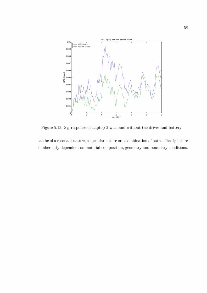
58
2 3 4 5 6 7 80
0.001
0.002
0.003
0.004
0.005
0.006
0.007
0.008
0.009
0.01
freq (GHz)
S21
(lin
ear)
NEC laptop with and without drives
with drives without drives
Figure 5.13: S21 response of Laptop 2 with and without the drives and battery.
can be of a resonant nature, a specular nature or a combination of both. The signature
is inherently dependent on material composition, geometry and boundary conditions.

59
Chapter 6
Conclusions
6.1 Conclusions
Detecting resonances and signatures of structures requires antennas with certain ra-
diating properties. These properties consist of high gain, minimal side lobes and
narrow beamwidths. The double ridged horn antenna designed for this application
has proven to be beneficial due to its broadband operation and high gain. The conical
spiral antenna, while broadband, has poor directivity and a broad main lobe which
inherently contributes to unwanted reflections.
Simple and complex devices exhibit unique signatures when illuminated with elec-
tromagnetic energy. Microstrips that are an odd multiple of λ/2 in length exhibit a
resonant response. As the strip becomes wider, the resonant peak begins to shift
slightly lower. As the strip width approaches that of a square, the resonant peak
diminishes and the response becomes high pass in nature.
When multiple microstrips are placed on a single target and illuminated, contribu-
tions from each of the strips are evident in the received response. These components
only exist when the strips are spaced approximately λ/2 apart. As the spacing de-
creases, then complex field interactions begin to dominate and the response becomes
unpredictable.
When illuminating complex devices, such as a laptop computer, the signatures
become more complex in nature. Material thickness, metal power and ground planes,

60
microstrip traces and differences in various boundary intrinsic impedances all con-
tribute to the resulting unique signature.
6.2 Future Research
There are many unexplored avenues in which this research could branch:
• Specular responses from targets need to be analyzed where the wavelength is
much smaller than the physical size of the target. Utilizing an automated
positioner would provide consistent and repeatable results.
• Devise an algorithm that unwinds the electrical distance out of the phase re-
sponse of the target so that meaningful phase content may be extracted and
analyzed.
• Develop an antenna calibration that provides a calibration plane at the radiating
end of the antenna.
• In depth use of an electromagnetic simulator to explore theoretical responses of
complicated structures and devices, and bypassing obstacles such as imperfec-
tions in the test environment and antenna deficiencies.
• In depth analysis of complex metallic and dielectric boundary scenarios.

61
Bibliography
[1] J. D. Kraus and R. J. Marhefka, Antennas: For All Applications, McGraw-Hill
Publications, 2002.
[2] C. A. Balanis, Antennas Theory: Analysis and Design, John Wiley and Sons,
2002.
[3] S. Ramo, J. R. Whinnery and T. Van Duzer, Fields and Waves in Communi-
cation Electronics, Wiley Publications, 1994.
[4] U. S. Inan and A. S. Inan, Electromagnetic Waves, Prentice Hall, 2000.
[5] E. F. Knott, J. F. Shaeffer and Michael T. Tuley, Radar Cross Section, Artech
House, 1993.
[6] S. B. Cohen, “Properties of the ridge waveguide,” Proceedings IRE., August
1947, pp. 783-789.
[7] K. L. Walton and V. C. Sundberg, “Broadband ridged horn design,” Mi-
crowave Journal., March 1964, pp. 96-101.
[8] F. Leferink and D. Boerle, “High field strength in a large volume: the extended
double ridged guide vs. the biconical and log periodic antenna,” Proc IEEE.,
1998, pp. 339-344.
[9] IEEE Standard Test Procedures for Antennas, IEEE Std 149-1979, published
by IEEE, Inc., 1979.

62
[10] IEEE Standard Definitions of Terms for Antennas, IEEE Std 145-1983, pub-
lished by IEEE, Inc., 1983.
[11] T. W. Hertel and G. S. Smith, “The conical spiral over the ground,” IEEE
Trans. Antennas Propagat., Vol. 50, NO. 12, pp. 1668-1675, December 2002.
[12] D. W. Smith, “Spiral antennas over a ground plane,” IEEE Antennas and
Propagation Society Int Symp., Vol. 4, pp. 2093-2096 Jul 1992.
[13] D. M. Sheen, D. L. McMakin and T. E. Hall, “Three-dimensional millimeter-
wave imaging for concealed weapon detection,” IEEE Trans. Microwave The-
ory and Techniques, Vol. 49, NO. 9, pp. 1581-1592, Sept. 2001.
[14] “Security Technology,” IEEE Aerospace and Electronic Systems Magazine,
Vol. 15 Issue: 10, pp. 131-136 Oct 2000.