charge-based superconducting digital logic family using quantum … · 2018-01-03 · circuit...
TRANSCRIPT

1
Charge-based superconducting digital logic familyusing quantum phase-slip junctions
Uday S. Goteti and Michael C. Hamilton
Abstract—Superconducting digital computing systems, primar-ily involving Josephson junctions are actively being pursued ashigh performance and low energy dissipating alternatives toCMOS-based technologies for petascale and exascale computers,although several challenges still exist in overcoming barriersto practically implement these technologies. In this paper, wepresent an alternative superconducting logic structure: quantizedcharge-based logic circuits using quantum phase-slip junctions,which have been identified as dual devices to Josephson junctions.Basic principles of logic implementation using quantum phase-slips are presented in simulations with the help of a SPICE modelthat has been developed for the quantum phase-slip structures.Circuit elements that form the building blocks for complex logiccircuit design are introduced. Two different logic gate designs:OR gate and XOR gate are presented to demonstrate the usageof the building blocks introduced.
Index Terms—Charge-based logic, Josephson junctions, Quan-tum phase-slips, Single-flux-quantum logic, Superconductingnanowires.
I. INTRODUCTION
ENERGY efficiency for high-performance computing is agrowing concern, especially in realizing peta-scale and
exa-scale computers [1]. Single-flux quantum logic familiesbased on Josephson junctions are actively being pursued as analternative to CMOS technologies to overcome these problems[2], although several challenges are yet to be overcome [3].In this paper, we introduce a quantized charge-based super-conducting logic family using quantum phase-slip junctions(QPSJs), as an alternative to JJ-based SFQ circuits, whichmay overcome these challenges by having advantages suchas voltage biasing and simpler design while including all thebenefits of SFQ circuits.
Quantum phase-slip is a superconducting phenomenonwhere the phase difference across a one dimensional nanowirechanges by 2π with the suppression of the superconductingorder parameter to zero. This has been observed as a resistancetail below superconducting transition in experiments [4], [5],[6]. This phenomenon has been identified as dual to Josephsontunneling based on charge-flux duality [7]. A charge tunnelsbetween two superconducting regions, across an insulatingbarrier, in a Josephson junction, inducing a flux quantum in thecorresponding loop. A QPSJ can be viewed as flux tunnelingacross a superconducting nano-wire (barrier for flux) creatinga voltage drop at the ends of the wire [8]. Therefore, under theappropriate operating conditions, QPSJs can be configured to
Uday S. Goteti and Michael C. Hamilton are with the Department ofElectrical and Computer Engineering, Auburn University, Auburn, AL, 36830USA e-mail: [email protected]
Manuscript received December 29, 2017.
generate quantized-area current pulses analogous to constant-area voltage pulses in SFQ circuits [9]. We have developed aSPICE model for QPSJs based on a dual model to JJs [10]and demonstrated in simulations, the constant-area pulses thatdemonstrate quantized charge transport, corresponding to aCooper pair in QPSJs. In order to implement logic circuits withthese devices, a charge-island circuit element, analogous to anSFQ loop [9], [11], [12], [13], [14], has been implemented,based on single-charge transistor circuits [15], [16].
In the next section, the basic circuit elements for charge-based superconducting logic are presented along with designand operation requirements that can be expected to produceand manipulate the quantized-charge pulses. These circuitsrepresent the building blocks, that, when used together in dif-ferent combinations, can form various logic gates that can beused to scale-up the logic operations to perform more complexcomputations. Finally, the design examples and simulationresults of some of the logic gates using the basic componentsis presented.
II. LOGIC CIRCUIT ELEMENTS
The current pulses representing Cooper pair transport acrossthe phase-slip center in the superconducting nanowire form thelogic bits, with the presence of the pulse representing logic”1” and absence of the pulse representing logic ”0”. Whena QPSJ is operated below its critical voltage VC , the currentthrough the device is zero, and the phase-slip center acts as aninsulating barrier between the two electrodes of the device. Asan input voltage pulse above the critical voltage is applied to anover-damped QPSJ, an electron pair tunnels across the phase-slip center generating a current pulse with a constant areaequal to the charge of two electrons. Therefore, this operationcorresponds to a switching from ”0” to ”1” in charge-basedlogic. All the other logic operations can be performed by usingone or a combination of several logic circuits discussed below.
A. Charge island
The charge-island is comprised of two QPSJs and a capaci-tor. The two junctions can be identical or different dependingon the application in the logic circuit. A circuit schematicof the island is shown in Fig. 1. When phase-slip occurs inboth the junctions, the node 1 between both the QPSJs isisolated from the rest of the circuit acting as an island thatcan hold a charge of C.VC , where C is the capacitance of thecapacitor. This circuit is a superconductor analog to a single-electron transistor [17]. In this logic operation, the charge onthe island will be restricted to a single Cooper pair, i.e. 2e.
arX
iv:1
801.
0071
5v1
[ph
ysic
s.ap
p-ph
] 2
Jan
201
8

2
Fig. 1. Charge island circuit schematic to generate and/or latch charge onnode 1. Note that the capacitance C can be a parasitic capacitance associatedwith the particular circuit design and layout.
Fig. 2. Simulation result of an island circuit shown in Fig. 1, illustratingconstant-area current pulse of area = 2e. The critical voltage of both junctionsgiven by VC = 0.7 V. Capacitance C = 1
22e/VC , voltage bias Vb = 1 mV,
and magnitude of the pulse input voltage Vin = 2 mV.
Both the junctions Q1 and Q2 are biased by DC voltage Vbsuch that the voltage across each junction does not exceed thecritical voltage VC of either junction. The input voltage Vin isa pulse signal that can drive the junction Q1 above its criticalvoltage VC and generate a current pulse. The circuit shownin Fig. 1 can be designed to accommodate either no chargeon the island at an instant, or one Cooper pair dependingon the application by appropriately designing the capacitor.If the capacitance C < 2e/VC , the capacitor cannot hold thecharge generated by exciting Q1 above its critical voltage,and therefore immediately switches the junction Q2. But ifthe capacitance C > 2e/VC , then the island traps the chargeuntil another pulse signal drives it to the output. Note that thiscircuit can be connected to another circuit instead of Vin touse the incoming current pulse to Q1 to drive the connectedcircuit.
The circuit operation is illustrated using WRSPICE simula-tion, through demonstration of a constant-area current pulse asshown in Fig. 2. Different configurations of this circuit can beused in conjunction with other circuits to design several logicgates, some of which are shown in the following sections.
Fig. 3. Two input control/buffer circuit with input Vin2 acting as en-able/control signal. This circuit can be used as a direction control buffer circuitwhen Vin2 is DC bias. VC (Q2) > VC (Q3) > VC (Q1).
Fig. 4. Simulation result of a control circuit shown in Fig. 3, illustratingcurrent pulse at the output only when the control signal is low. The criticalvoltage of junction Q1 is 0.7 mV, Q2 is 1 mV and Q3 is 1.5 mV. CapacitanceC = 0.23 fF, Voltage bias Vb = 1.1 mV, magnitude of the pulse input voltageVin1 = 1.5 mV and magnitude of the control input voltage is Vin2 = 1 mV.(a) Input current pulses. (b) Control voltage signal. (c) Output current pulses.
B. Control/Buffer circuit
The control/buffer circuit configuration is unique to charge-based logic, while the charge island is analogous to a flux loopin SFQ circuits [9].
In the simplest version of this circuit, three QPSJs ofdifferent device parameters are used along with two capacitors.It has two input terminals for DC/pulse voltage sources anda DC voltage source for biasing the junctions. This circuitis shown in Fig. 3. The junctions are designed such that thecritical voltage of Q2 is higher than the critical voltage of Q3.The input voltage Vin2 has magnitude of 0.7VC where criticalvoltage of Q3 is VC . The input voltage Vin1 is significantlyhigher than the critical voltage of Q1 to be able to generate thecurrent pulse. Therefore, when the current pulse is generatedat Q1, it switches Q3 before Q2 when the input Vin2 is highand produces the output ”0” at node 4. But when the inputVin2 is low, the output is the same as the input Vin1, as thejunction Q2 is biased by Vb. Hence, the input Vin2 acts asthe enable/control input. Furthermore, if the critical voltageof Q1 is lower than critical voltages of Q2 and Q3, then thecircuit becomes unidirectional, only allowing the current fromnode 1 to node 4. The input Vin2 can be a DC bias to use

3
this circuit as a buffer. The simulation result of an exampleoperation of this circuit is illustrated in Fig. 4, with circuitparameters chosen to satisfy the conditions mentioned above.
III. LOGIC GATES
The charge island and the control/buffer circuit, in theirdifferent configurations, can be used in various possible con-figurations to design several logic gates or memory circuits. Insome cases, it is possible to realize the same logic operationsin different circuits. Some examples of logic gates designedusing combinations of logic elements discussed in the previoussection are presented below.
A. OR gate
The OR gate design discussed here predominantly usescharge islands with different parameters in its operation.However, the buffer circuit is added in the circuit to preventdata flow in directions other than that which is intended.Therefore, this circuit is a good example to illustrate differentcombinations of logic elements to achieve desired operation.The circuit schematic for a two-input OR gate is shownin Fig. 5. The two inputs terminals are connected to pulsevoltage sources Vin1 and Vin2, but they can also be incomingcurrent pulses from another circuit. The input branches haveQPSJs that generate or simply transmit the current pulses withthe capacitors at nodes 3 and 6 acting as the islands. Thecapacitance of capacitors at these nodes are designed to havevalues C < 2e/VC . The current from either of the inputsimmediately switch Q4 and transmit the data further. JunctionQ3 acts as the buffer circuit preventing the current pulse fromone input in to the other. This is possible by designing Q3to have lower critical voltage than Q1 and Q2, but higherthan Q4. The island at node 8 functions similarly as islands atnodes 3 and 6. The charge island formed by devices Q5, Q6and C ′ are designed such that the charge 2e can be trappedat node 9, and an external force from clock Vclk is necessaryto drive the trapped charge to output terminal. Therefore, witheither input high, the charge 2e appears at node 9, with highoutput synchronized to the clock signal. When both the inputsare high, the result is the same, with the additional charge 2efollowing the path through Q3 to the ground. The output islow, only when both the inputs are low, since the clock signalalone will not be able to switch any of the junctions.
This design is similar to an OR gate in SFQ circuits [9],with island formed at Q5, Q6 and C ′ analogous to a twojunction JJ interferometer and both the individual branchesup to this island forming a circuit analogous to Josephsontransmission line, with some differences in the operation ofbuffer circuit. An example simulation result of this circuit withselected parameters is shown in Fig. 6. AND and XOR logicoperations can be achieved using similar circuits. In an ANDgate, the charge trapping island is replaced by additional buffercircuit. While, in an XOR gate, the charge trapping island iscompletely removed.
Fig. 5. Two-input OR gate design with multiple charge islands in series.Critical voltages of junctions satisfy the conditions VC(Q4, Q5, Q6) <VC(Q3) < VC(Q1, Q2), capacitance C < 2e/VC(Q1) and4e/VC(Q5, Q6) > C′ > 2e/VC(Q5, Q6). Magnitudes of inputs Vin1 andVin2 are 1.5VC(Q1, Q2), and that of clock Vclk is 1.5VC(Q4, Q5, Q6).DC voltage biases have values of 0.7VC(Q1, Q2).
Fig. 6. Simulation result of a two-input OR gate shown in Fig. 5. The criticalvoltages of junctions Q1, Q2 is 1.5 mV, Q3 is 0.7 mV and Q4, Q5, Q6 is1 mV. Capacitance C = 0.23 fF and C′ = 0.6 fF, Voltage bias Vb = 0.7 mV,magnitude of the pulse input voltages Vin1, Vin2 = 1.5 mV and magnitudeof the clock is Vclk = 0.7 mV. (a) Input current pulses from Q1. (b) Inputcurrent pulses from Q2. (c) Output current pulses.
Fig. 7. Two input XOR gate with both inputs Vin1 and Vin2 connected totwo different terminals of the circuit each. VC (Q2, Q5) > VC (Q3, Q6) >VC (Q1, Q4). Vin1, Vin2 have magnitudes of 1.5VC (Q1, Q4). C < 2e/VC
4
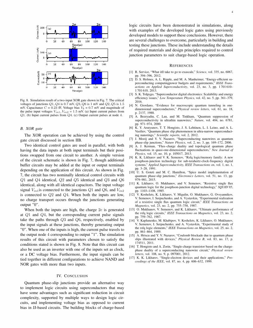
Fig. 8. Simulation result of a two-input XOR gate shown in Fig. 7. The criticalvoltages of junctions Q1, Q4 is 0.7 mV, Q3, Q6 is 1 mV and Q2, Q5 is 1.5mV. Capacitance C = 0.23 fF, Voltage bias Vb = 0.7 mV and magnitude ofthe pulse input voltages Vin1, Vin2 = 1.5 mV. (a) Input current pulses fromQ1. (b) Input current pulses from Q4. (c) Output current pulses at node 4.
B. XOR gate
The XOR operation can be achieved by using the controlgate circuit discussed in section IIB.
Two identical control gates are used in parallel, with bothhaving the data inputs at both input terminals but their posi-tions swapped from one circuit to another. A simple versionof the circuit schematic is shown in Fig. 7, though additionalbuffer circuits may be added at the input or output terminalsdepending on the application of this circuit. As shown in Fig.7, the circuit has two nominally identical control circuits withQ1 and Q4 identical, Q2 and Q5 identical and Q3 and Q6identical, along with all identical capacitors. The input voltagesignal Vin1is connected to the junctions Q1 and Q6, and Vin2is connected to Q2 and Q4. When both the inputs are low,no charge transport occurs through the junctions generatingoutput ”0”.
When both the inputs are high, the charge 2e is generatedat Q1 and Q4, but the corresponding current pulse signalstake the paths through Q3 and Q6, respectively, enabled bythe input signals at these junctions, thereby generating output”0”. When one of the inputs is high, the current pulse travels tothe output node 4 corresponding to output ”1”. The simulationresults of this circuit with parameters chosen to satisfy theconditions stated is shown in Fig. 8. Note that this circuit canalso be used as an inverter with one of the inputs set as clock,or a DC voltage bias. Furthermore, the input signals can betied together in different configurations to achieve NAND andNOR gates with more than two inputs.
IV. CONCLUSION
Quantum phase-slip junctions provide an alternative wayto implement logic circuits using superconductors that mayhave some advantages such as significant reduction in circuitcomplexity, supported by multiple ways to design logic cir-cuits, and implementing voltage bias as opposed to currentbias in JJ-based circuits. The building blocks of charge-based
logic circuits have been demonstrated in simulations, alongwith examples of the developed logic gates using previouslydeveloped models to support these conclusions. However, thereare several challenges to overcome, particularly in building andtesting these junctions. These include understanding the detailsof required materials and design principles required to controljunction parameters to suit charge-based logic operation.
REFERENCES
[1] R. Service, “What itll take to go to exascale,” Science, vol. 335, no. 6067,pp. 394–396, 2012.
[2] D. S. Holmes, A. L. Ripple, and M. A. Manheimer, “Energy-efficient su-perconducting computingpower budgets and requirements,” IEEE Trans-actions on Applied Superconductivity, vol. 23, no. 3, pp. 1 701 610–1 701 610, 2013.
[3] S. K. Tolpygo, “Superconductor digital electronics: Scalability and energyefficiency issues,” Low Temperature Physics, vol. 42, no. 5, pp. 361–379,2016.
[4] N. Giordano, “Evidence for macroscopic quantum tunneling in one-dimensional superconductors,” Physical review letters, vol. 61, no. 18,p. 2137, 1988.
[5] A. Bezryadin, C. Lau, and M. Tinkham, “Quantum suppression ofsuperconductivity in ultrathin nanowires,” Nature, vol. 404, no. 6781,pp. 971–974, 2000.
[6] K. Y. Arutyunov, T. T. Hongisto, J. S. Lehtinen, L. I. Leino, and A. L.Vasiliev, “Quantum phase slip phenomenon in ultra-narrow superconduct-ing nanorings,” Scientific reports, vol. 2, 2012.
[7] J. Mooij and Y. V. Nazarov, “Superconducting nanowires as quantumphase-slip junctions,” Nature Physics, vol. 2, no. 3, pp. 169–172, 2006.
[8] A. J. Kerman, “Flux–charge duality and topological quantum phasefluctuations in quasi-one-dimensional superconductors,” New Journal ofPhysics, vol. 15, no. 10, p. 105017, 2013.
[9] K. K. Likharev and V. K. Semenov, “Rsfq logic/memory family: A newjosephson-junction technology for sub-terahertz-clock-frequency digitalsystems,” Applied Superconductivity, IEEE Transactions on, vol. 1, no. 1,pp. 3–28, 1991.
[10] U. S. Goteti and M. C. Hamilton, “Spice model implementation ofquantum phase-slip junctions,” Electronics Letters, vol. 51, no. 13, pp.979–981, 2015.
[11] K. Likharev, O. Mukhanov, and V. Semenov, “Resistive single fluxquantum logic for the josephson-junction digital technology,” SQUID’85,pp. 1103–1108, 1985.
[12] V. Koshelets, K. Likharev, V. Migulin, O. Mukhanov, G. Ovsyannikov,V. Semenov, I. Serpuchenko, and A. Vystavkin, “Experimental realizationof a resistive single flux quantum logic circuit,” IEEE Transactions onMagnetics, vol. 23, no. 2, pp. 755–758, 1987.
[13] O. Mukhanov, V. Semenov, and K. Likharev, “Ultimate performance ofthe rsfq logic circuits,” IEEE Transactions on Magnetics, vol. 23, no. 2,pp. 759–762, 1987.
[14] V. Kaplunenko, M. Khabipov, V. Koshelets, K. Likharev, O. Mukhanov,V. Semenov, I. Serpuchenko, and A. Vystavkin, “Experimental study ofthe rsfq logic elements,” IEEE Transactions on Magnetics, vol. 25, no. 2,pp. 861–864, 1989.
[15] A. Hriscu and Y. V. Nazarov, “Coulomb blockade due to quantum phaseslips illustrated with devices,” Physical Review B, vol. 83, no. 17, p.174511, 2011.
[16] T. Hongisto and A. Zorin, “Single-charge transistor based on the charge-phase duality of a superconducting nanowire circuit,” Physical reviewletters, vol. 108, no. 9, p. 097001, 2012.
[17] K. K. Likharev, “Single-electron devices and their applications,” Pro-ceedings of the IEEE, vol. 87, no. 4, pp. 606–632, 1999.