charge-coupled-device/fiberoptic for protein crystallography/67531/metadc686058/... · a large...
TRANSCRIPT

Charge-coupled-device/fiberoptic 'taper array X-ray detector for protein crystallography
Istvan Naday, Stephen Ross, Edwin M. Westbrook, George Zentai
Argonne National Laboratory, 9700 South Cass Avenue, Argonne, IL 60439 L'rc;r c I-
. ABSTRACT
A large area, charge-couple-device (CCD) based fiberoptic taper array detector (APS-1) has been installed at the insertion-device beamline of the Structural Biology Center at the ANL Advanced Photon Source. The detector is used in protein crystallography diffraction experiments, where the objective is to measure the position and intensity of X-ray Bragg peaks in diffraction images. Large imaging area, very high spatial resolution, high X-ray sensitivity, good detective quantum efficiency, low noise, wide dynamic range, excellent stability and short readout time are all fundamental requirements in this application. The APS-1 detector converts the two-dimensional X-ray patterns to a visible light images by a thin layer of X- ray sensitive phosphor. The phosphor coating is directly deposited on the large ends of nine fiberoptic tapers arranged in a 3x3 array. Nine; thermoelectrically cooled 1024 x 1024 pixel CCD's image the patterns, demagnified by the tapers. After geometrical and uniformity corrections, the nine areas give a continuous image of the detector face with virtually no gaps between the individual tapers. The 18 parallel analog signal-processing channels and analog-to-digital converters assure short readout time and low readout noise.
Keywords: CCD, fiberoptic taper, X-ray diffraction, crystallography, imaging detector. .
1. INTRODUCTION
Crystals, placed in a single wavelength, collimated X-ray beam, diffract the incident beam in defined directions, described by Bragg's Law '. In protein crystallography measurements, the crystal under study is rotated about an axis perpendicular to the x-ray beam, permitting Bragg spots to pass through their appropriate orientation for diffraction. These spots diffract over a wide solid angle, which can be recorded by a two dimensional, X-ray sensitive detector. In one data set, several hundred images are recorded over the rotation angle range of the crystal '. Each image might contain several thousand Bragg peaks. The structure of protein molecules can be solved by analyzing the intensities and positions of the recorded Bragg peaks. Even the weakest peaks must have enough number of photons, to achieve reasonably high statistical precision. There is a continuous effort to increase the X-ray beam intensity of X-ray sources. The
tunability and small beam divergence, has created many new opportunities in the field of protein crystallography. With the use of high intensity synchrotron X-rays and high efficiency, large area, high dynamic range, fast, electronic readout X-ray imaging detectors, new crystal structures can be solved.
' advent of synchrotron X-ray sources over the past two decades, with their very high flux, wavelength

DISCLAMER
Portions of this document may be illegible in electronic image products. Images are produced from the best avahble original document.

2. REQUIREMENTS
The detector requirements are very demanding in protein crystallography measurements. Table: 1. gives a summary of the most important minimum requirements:
X-ray sensitive area: Pixel resolution: Spatl ai resolution: better Wan 80um at FWHM . Dynamic range: better than 5000
’ Detective Quantum Efficiency: . higher than 70% (strong peaks) X-ray efficiency: more than 80% Readout time:
iargeithan 100 x 100 mm2 more than 1000 x 1000 pixels
better than 800um at FWO.01M
less than 2 sec (synchrotron)
Table 1. Summary of requirement of X-ray detectors for Synchrotron Protein Crystallography
The APS-1 detector is shown in Fig.1, before the deposition of the X-ray converter phosphor coating.
h.1. Sensitive Area
Figure 1. Front view of the APS-1 X-ray detector.
In protein crystallography experiments, X- rays are diffracted in large angles by the studied crystal. In some cases the diffraction angle might reach 90 degrees. This results in a large X-ray image even if the crystal-to- detector distance is small. The detector should ideally cover the full diffraction image. If the sensitive area of the detector does not cover the full diffraction image, the area can be scanned in consecutive runs, but this would result in extended experimental time and higher radiation damage to the crystal3. Large detector area allows larger- . crystal-to-detector distances, resulting in lower scattered X-ray background at the detector. Since the CCD sensor area is limited, the image must be demagnified. Signal loss (light loss) in the detector is proportional with the square of the optical demagnification. The optimum demagnification for a protein crystallography CCD detector can be estimated based on the parameters of the experimental setup‘”. Light loss and technological problems limit the practical demagnification to approximately 4: 1. If larger area is required, an array of
,
fiberoptic tapers and CCDs should be used. In the APS-1 detector the 210x210 &I’ active area is covered by a 3x3 array of fiberoptic tapers. The reduction of each fiberoptic taper is approximately 2.9:l.

2.2. Geometrical resolution
The angular divergence of the beam of synchrotron X-ray sources is very low, cons&uently .the size of Bragg peaks a t the detector i s primarily determined by the size of the crystal under study or by the X-ray beam diameter at the crystal, whichever is the smaller. The divergence of the X-ray beam at the A P S SBC- 19ID beamline is 0.02 degree, and the beam diameter is approximately O.lmm, the typical crystal Si is between 0.05 and 0.3 mm. In a high resolution diffraction image the expected number of the Bragg peaks might exceed 16. The difference in the diffrslction angle between two adjacent Bragg peaks can be as low as 0.5 degree. Assuming a detector-to-crystal distance of 100 millimeters, intensities of Bragg peaks, 800- 1000 pm apart shodd be determined with high accuracy. This requirement defines the required geometrical resolution and the point spread behavior of the detector.
2.3. Dynamic range
The intensities of the strongest and weakest peaks may vary as more than lo4 in a'diffraction image. For the determination of a protein crystal structure all Bragg peak intensities should be measurable with reasonably high accuracy.
The uncertainty in the measured value of a Bragg peak is fundamentally defined by the number of X-ray photons within the peak. Several other factors degrade the accuracy, such as read noise, dark current noise, uncertainty introduced during the image correction procedures, instabilities of the detector electronics, nonlinearity of the detector response, digitization noise, etc.
The simplified formula for the calculation of the dynamic range of a pixel in the detector is given by
JRN~+DC*T, DR = F y
where FS is the number of electrons in the pixel at full scale signal of the AID (65335 ADU's) RN is the rms value of the read noise in electrons DC is the dark current of a pixel at the operating temperature of the detector in electrons T~xp is the exposure time
Due to the very high intensity of the synchrotron X-ray beam, the typical exposure time range in protein crystallography measurements is 0.01s to 1s. The dark current can be as high as 70 electrons/s (worst case) at -35 OC CCD temperature if front illuminated, non MPP CCD's are used.
2.4. Sensitivity
In the APS-1 detector, X-rays are converted to visible light by a thin layer of phosphor, deposited on the large ends of the fiberoptic tapers (see the discussion of the optical design below). The light photons travel through a demagnifier fiberoptic taper. The CCDs are attached to the small end of the tapers by optical coupling gel. The approximate overall conversion gain is given by the formula:
* C, * QE Gain=
where Gain is the overall conversion gain in electrodX-ray photons GPbosphoris effective phosphor gain: the number of light photons entering the fiberoptic taper,
L is the edge length of the larger end of the fiberoptic taper generated by a single X-ray photon.

e is the edge length of the smaller end of the fiberoptic taper C,, isthe coupling efficiency between the CCD and the FO taper (approx. 0.7) QE is the quantum efficiency of the CCD at the emission wavelength of the phosphor
(approximately 0.25.B 550nm)
The expected conversion gain is approximately 5 electrons / X-ray photon @ 12 keV X-ray energy.
. The actual g a b is slightly lower, due to the attenuation of the protective cover in fiont of the phosphor. The X-ray attenuation of a thin, aluminized polyester foil is less then 5% at 12keV X-ray energy.
2.5. Dark noise
The dark current noise of the detector should be negligible under normal operation . The exposure time is normally below ls/frame in protein crystallography measurements at the APS 19ID beamline. The calculated dark noise of the fiont illuminated, non-MPP CCD is less then 9 electron rms / pixel assuming -35 OC CCD temperature and 1 second exposure time. This noise is negligible compared to the expected read noise and to the noise introduced by the scattered X-ray radiation in the experiment. We decided to use non-MPP, fiont illuminated CCD’s because of their higher full well capacitance and lower price.
The read noise of the CCD depends on the required readout time. With shorter readout times the bandwidth of the analog signal processing chain must be larger, resulting in higher noise. At 3.2 ps / pixel readout speed, lower then 25 electron rms/pixel noise is achievable. This will give a dynamic range of approximately 12,000 /pixel.
2.6 Readout time
As it is described in 2.3, there is a compromise between the pixel readout time and readout noise. At a given pixel readout time, the total readout time of the array can be reduced by increasing the number of pixels read simultaneously. In the APS-1 detector we used the SiTe, Inc. TK1024 two-port CCD’s (two outputs on the opposite ends of the serial registers) and 3.2 ps pixel readout time. The number of parallel analog-signal-processing channels and ADC’s can be calculated
The APS-1 detector has 18 parallel analog-signal-processor and ADC channels: 9 CCD’s with 2 outputs, each.
The frame readout time of a two-port CCD can be calculated:
where
Readout time of a CCD Number of pixels in the vertical direction (Parallel pixels) (1024) Parallel shift time (1 8 p) Number of active pixels in the horizontal direction (Active Serial pixels) (1024) Pixel readout time (3.2 ps) Number of pixels in the “lead-in” part of the serial register (50) Shift time /pixel in the “lead-in” part of the serial register (0.4s)
The readout time in the APS-1 detector is 1.7 sec / frame.
The APS-1 detector can be operated in 2x2 binned mode. In this case, the pixel resolution is’ 1536 x 1536 pixels, with a readout time of approximately 0.44 sec / frame.

3. DESIGN AND OPERATION
To fulfill the' detector design requirements, the detector has 3~3'sections, each having a 70mm-to-24mni fiberoptic demagnifier and a 1024 x 1024 pixel CCD, attached to the tapers. .
3.1. Mechanical design
The detector has two major parts: the electro-optical assembly'and the electronics sections. The electro- optical section holds the 3x3 taper array and the CCD assemblies. This section is filled with dry argon gas during normal operation to avoid condensation or icing on the cooled sensors and to reduce thermal conductance between the CCD's and the case. The electronics section is the back part of the detector. Nine identical electronics modules are attached to the water cooled heat exchanger plate. This plate cools the warm side of the thermoelectric coolers at its front side and removes the heat generated in the electronic modules through thermal couplers inside each electronic module at the back side. The preamplifier circuits are mounted on nine individual assemblies. The preamplifier boards extend into the electro-optical enclosure. The design of these assemblies assures hermetic seal around the openings for the preamplifier boards.
Thannodlectric positioning
Piberoptic taper
Figure 2. One of the nine CCD assemblies of the APS-1 detector.
Nine fiberoptic tapers are cemented together with very small physical gap between them. The gap is less then 100 pm between the modules. The tapers are surrounded by a metal frame made of Kovar to reduce the thermal expansion difference between the taper glass and the support fiame. A double groove has been machined close to the outer edge of the tapers to reduce forces on the glass parts during thermal cycling. The front face was polished after the assembly of the taper-array, forming a planar surface for the phosphor deposition. The taper array was manufactured by Schott Fiber Optics, Inc.
The CCDs are coupled by optical gel to the smaller end of the taper. After optical alignment, the CCD assemblies are supported by individual, X-shaped flat springs against the tapers. The CCD assembly is shown in Fig.2. Traces on the CCD socket printed circuit board makes all connections between the pins of the

sensor. After mechanical assembly of the detector, a flexible wire-bundle, attached to this board is connected to a miniature multipin connector on the preamplifier. A small copper block connects the cold side of the two stage thermoelectric cooler (TEC) to the CCD case. The warm side of the TEC is accessible by the heat transfer assembly, mounted on the water cooled heat exchanger plate. The assembled front end, viewed from the rear ofthe detector, is shown in Fig.3. The heat exchanger plate with the nine flexible thermal couplers, can be seen in Fig.4.
Figure 3. Rear side of the electro-optical section . Figure 4. The heat-exchanger plate with of the detector, before assembly. the nine thermal couplers.
The electronic circuitry consists of four printed circuit boards for each module. These boards are fastened to the four sides of an internal aluminum block to assure good thermal conductivity between the block and the surface-mount circuitry. The electronic modules are easily removable for servicing. The control signals and power supply voltages are connected to the electronic modules through a set of connectors at the rear end of the modules. The separate CCD controller and interface board is mounted on the back side of the electronics section.
3.3,. Optical design
X-ray photons are converted to visible light by a thin layer of phosphor deposited directly on the front surface of the fiberoptic taper array. The phosphor material is Gd202S:Tb, with an average grain size of 6 pm. We used the phosphor settling method to coat the face of the detector with approximately 17 mglmm' phosphor density. A thin, aluminized polyester foil placed on top of the phosphor layer serves two purposes: it acts like an optical reflector and forms the back sheet of a protective "pillow", covering the full X-ray sensitive area of the detector. The reflector increases the effective light output of the phosphor by approximately 30%, reflecting those light photons which leave the phosphor away from the taper surface. The use of the reflector degrades the spatial resolution of the detector because the light reflected back by

the shiny reflector foil is scattered over a larger area onto the fiberoptic surface. This causes longer tails of the spatial response curve. Due to the cooling of the attached CCDs, the temperature of the outer surface of the taper array may drop below the ambient temperature what might lead to condensation on the phosphor coating. To avoid condensation, the inflated pillow is placed in front of the X-ray sensitive area of the detector. The reflector foil forms the back of the pillow and an other foil, placed a few millimeters away is the front.sheet ofthe pillow. Dry nitrogen gas is pumped between the two layers, to assure adequate thermal insulation between the cold detector face and the ambient. At the same time the gas pressure pushes the reflector foil against the phosphor layer, assuring close contact between the phosphor and the reflector.
DATA ACQUISITION . HIPPI
> > DATA < > >
VME DATA DETECTOR HEAD
AND CCD CONTROLLER
I > ETRERNET M U L T I P m R
HIPPI INTERFACE SBC (167)
, . DESCRAHBLER (2x1 . / VHE m R Y ICRYSLIN) (2x1 SEm
- - I C TEC CONllRoL Y DETECTOR SETUP
AND MONITORING 1: : RS4221-, . ETfLERNET
a . < > > VME RS422 ' ' E422
> .==log > --- EPICS) b
RS422 DRIVER/RECTIVER PARALLEL T/O (*rcdnaq) AHAtoc WJLTIPLEXER AHAUX-20-DIGITAL CONVERTER SBC (167)
B I \
TNEPMXLECTSUC COOLER +2EV/2A -5.2V/3A CONmL?ZR 11) +15V/5A -15V/5A POWER UNITS 19x1 *5v/5A
19" 19"
WATER DETECTOR TEMPERATURE CONTROLLER CHILLER POWER
SUPPLY -*_ C$
Figure 5. Block diagram of the APS-1 detector system.
The tapers are machined in such a way that there is no dead area on the larger end of the taper. In other words: the full, 7Ox70mm' area is demagnified onto the 24 x 24 mm2 end. This results in some dead (black) areas, close to the edge of the smaller end of the taper. The CCDs are carefully aligned to image the full demagnified image. On the uncorrected image, a small, unused area is observable, close to the edges of the CCDs. Due to the pincushion distortion of the tapers, a straight line on the input of the detector appears to be a curved line on the CCD. After the application of geometrical correction6, these curved lines are restored to straight lines on the corrected image.
To reduce light loss and optical scatter at the optical interface between the small end of the fiberoptic taper and the CCD, the gap must be filled with optical coupling material. In some detector designs (and in one of our earlier detectors'**) the coupling is made by bonding the CCD's permanently to the tapers using optical epoxy. The permanent coupling has several disadvantages, e.g. in case of the failure of a CCD, the full taper array becomes unusable if the defective CCD can not be removed without damaging the taper.

3.3. Electronics design .
The block diagram of the APS-1 detector system is shown in F i g 5 The system contains of the following major components:
Detector head Water-cooler and Recirculator Detector Power Supply '
Thermoelectric Cooler Control Temperature Controller Data Acquisition VME Crate
0
0
0 Descrambler (2) 0 Memory module (2) 0 HIPPI interface
0 Detector Control VME Crate 0
0 RS422 module 0 Parallel I/O 0 Analog Multiplexer (operating parameters) 0 Analog-to-Digital Converter (operating parameters)
Motorola 167 Single Board "Jmputer Data receiver and multiplexer module
Motorola 167 Single Board Computer
Figure 6. Rear view of the APS-1 detector head, showing the electronic modules and the CCD controllerlinterface baard.
!We limit the scope of this publication to the I idetector head of the detector system. Other !parts of the detector system, such as the kontrol and data acquisition hardware and 'software, as well as the data correction 'software (flood field and geometrical Idistortion correction) and the experiment lcontrol software (EPICS) will be published /elsewhere. I 'Nine interchangeable, identical electronic lrnodules are mounted inside the electronics section. The interface and CCD controller board is attached to the back side of the electronics section as it is shown in Fig.6. jFig.7 shows the simplified block diagram of ithe APS-1 detector head.
I
I
1 i
6
... .:'

. fl& CH2 preanp
Preamp II f4 l4-Y CH7
Detector s e w (W ' f Icl > , INTERFACE
c r FPGA
c . CCD COMROLLER
lo DATA ACQUlSmON
6xlSh4biis seki ECL
c I \ W E crate . .
1 CONTROLVME crate
and DlSTRlBUTlON
frm D m C i O R POWER SUPPLY
J
!
Figure 7. Simplified block diagram of the APS-1 detector head.
Fig.8 shows a more detailed block diagram of one of the electronic modules. One module contains two analog-signal-processor chains and oneset of drivers for one CCD. An electronically controlled analog switch selects the input signal of the Analog-Signal-Processor (ASP) in the module. In normal operation, the inputs are fed by the output signals of to low noise, CCD preamplifiers. The preamplifiers are placed inside the electro-optical section, near the CCD chips, to reduce noise pickup. In test mode, the input of the ASP can be switched to a CCD signal simulator circuit, generating signals for the test of the correct operation of the system. The amplitude of the simulated CCD signal is adjustable under computerlcontrol. * In normal operation, the signal passes through a variable-gain amplifier to a shaping amplifier and the Double-Correlated Sampling (DCS) circuit. Each analog signal processing channel feeds its 16-bit resolution analog-to-digital converter. The digital outputs are multiplexed to a 16-bit wide data bus. The positive and negative voltage levels of each CCD gate driver signals and the DC voltages of the CCD sensors are controlled digitally through 8-bit digital-to-analog (DAC) converters. The required digital values are transferred serially to all digital-to-analog circuits in the detector head. .. .~ - I -. .
Q

"c" Channel (Lev
INPUT VARIABLE GAIN SHAPING
from CCD PREAMP
'D outpui
SELECTOR, AMPLIFIER AMPLIFIER Digital M INPUT VARIABLE GAIN SHAPING
A SIMULATOR 4 CCD SIGNAL banmu
Ampritude Control
SLOW DRIVERS
8 ch &bit DAC ' 8 ch 8-bit DAC
'ak
Figure 8. Block diagram of one of the nine electronic modules.
The following table shows the remotely adjustable parameters of the detector:
CCD drive signals and voltages: Parallel gates, high Parallel gates, low Transfer gates, high Transfer gates, low Serial gates, high Serial gates, low Summing Well, high
* Summing Well, low '0 Reset gate, high
p .

. . ’c- ’
CCD DC voltages: 4 OUtpUtDrain *. Reset- .. e t g a t e
Analog-Signal-Processor control: 70
0
-0 Test signal amplitude CCD power odoff
Gain (left and right section of the CCD, outputs C and D) Offset (baseline for left and right)
Mode (test mode: simulated CCD signal, normal mode) ControI
I
All these parameters can be adjusted separately for all 9 CCD’s in the APS-1 detector system by changing the values in the detector control software, allowing us to optimize CCD performance.
The CCD controller contains all the information necessary to clock the CCD through its various functional states, and ii implemented using a field programmable gate array (FPGA). The heat of this controller is a state machine which contains the sequence of CCD states. T h e e states are idle, exposure, clear line, vertical shift, pre-horizontal shift, horizontal shift and post horizontal shift There are additional states used when the CCD is run in binned mode. Thus, stepping through these stab, first the CCD is in an idle mode, where photocharge is removed without being sampled or digitized. When the external system requests an exposure, the state machine moves to the exposure state, which it maintains for the duration of the externally supplied “exposure’’ pulse. M e r the exposure terminates, and the image must be read out. The state machine then progresses to two nested loops, the outer loop consisting of vertical shifts (to move photocharge down a vertical row by activating the parallel CCD gate lines) and the inner loop consisting of horizontal shifts. Triggering the analog-to-digital converter is part of the horizontal inner loop, as is the loading of FIFO memories for eventual data transmission. If the CCD pixels are binned, the states looped here are slightly modified from a non-binned case. The state machine thus knows the state, the sequence of states, and how many times the states are to sequenced , inside or not part of a set of (at most two) nested
.
loops.
The state machine also contains tabulated entries which tell it how many “sub-pixelyy elements there are per pixel and the number of “short” elements. While a detailed explanation is complex, in essence this allows the state machine to create some states (e.g. a horizontal shift) which last a few microseconds (e.g. 64 sub- pixel elements, 100 ns long, to give all the edges for a three phase horizontal shift, but only 1 “short” element) or to create some other, longer states (e.g. a vertical shift) which lasts hundred of microseconds (e.g. 64 sub-pixel elements where nothing changes, 64 “short”~e1ements which can define the three phase vertical clock edges). In a sense this can all be regarded as more levels of looping - sub-pixel, short, then the above described inner, and outer loops, allowing for microsecond horizontal shifts and millisecond vertical shifts.
The state machine ultimately drives a look-up table, which in turn controls a set of digital multiplexers, which finally choose which pattern to put out to a particular pin of the CCD. The entire state machine occupies about 70 percent of a Xilinx 4013 FPGA, which includes control of the transmitting data FIFO’s and a large number of test patterns for error checking. e

4. PERFORMANCE
.
Table 2 summarizes the performance of the APS-1 detector system.
8 .
Sensitive area: Conversion gain (12keV): Point spread function curve:
Uniformity of response (X-ray flood): Geometrical distortion: Dead zone between segments: Detective Quantum Efficiency: Phosphor coating: CCDs:
Fiberoptic tapers: Optical coupling: Cooling:
' Interfaces:
210 x 210 mm2 9 M P h
70 pm (FWHM) 750 pm (WO.OIM)
5% rms 1% 280, pm
> 75% @ I O % signal level P43 9, front illuminated, nonMPP, front-illuminated
1024xl024 pixel imagers with 2 outputs each 9, demagnification=286x optical gel between fiberoptic taper and CCD -35 Co, chilled water + regulated thermoelectric cooling Detector setup and control: Unix based EPiCS
Data Acquisition: VMUHiPPi
,
FULL RESOLUTION 2x2 pixel BINNING
Pixels 3072 x 3072 1536 x 1536
Pixel size at input (avg.) 69 pm 138 pm Conversion gain at 12 keV 6 M P h 6 M P h Read noise 35 e- rmslpixel e 30 e- rmslpixel
Pixel saturation > 330,000 e-lpixel > 500,000 &pixel Dark current (tc,=-35 Co) 65 e-lslpix. < 260 &slpix Dark current noise (texp-5s) - 8 e- rmslpixei Dynamic range (&= 1 s) >10,000 >15,000 CCD's CCD output amplifiers 18 18 Pixel readout time 3.2 pm 3.2 pm
image size 18 Mbyte 4.5 MByte
Active pixels >3000x3000 >I500 x I500
Digitization noise (16 bit ADC) 5e-rms 34-rms
- 16 XPh rmsfpixel
Readout time (fuii image) 1.7 s 0.44 s
ax.
Table 2. Measured performance of the APS-1 detector system.
The performance of the detector system has been evaluated in four stages:
0 Electronic tests Optical tests (visible light, with no phosphor coating) X-raytests Protein Crystallography tests
4.1. Electronic tests
During the electronic test, all parts of the detector system have been tested for correct operation. Noise levels, gain, linearity of the ASP channels, pulse shapes of the CCD drive signals, data transfer error rates, etc. have been measured. The short and long term stability of the detector gain and offset was also tested. Wc found all tested parameters in compliance with the design specifications

4.2. Optical tests.
-. . .. .>,
4
Before coating the detector with the X-ray converter phosphor layer, the optical parameters of the detector '
system were measured and evaluated. These test included:
-0 Uniformity tests (light flood field measurements) I
detect the effect of fiberoptic taper blemishes check the positioning of the CCD sensors detect any imperfections in the optical coupling between tapers and CCDs
-0
-0
Optical point-spread measurements 0 test the optical quality of the taper/CCD coupling
test the effect of the "bow" of the CCD chips
CCD transfer function measurements
0
verify the noise, linearity and saturation level of the CCD's determine the lightsensitivity (conversion gain) of the system
0 Dark current measurements
0
verify the individual dark cdrrent of the CCDs indirectly verify the operation temperature control system
0 Short and long term optical stability tests 0 check the mechanical stability of CCD positioning
verify the stable and reliable operation of the system
The optical tests were made on all modules of the detector. Some of the typical results are summarized in Fig.9 through Fig.13. All of these measurements were made by using a 560 nm wavelen,@ light-emitting diode (LED), visible light source., The LED was placed in a diffusing, integrating sphere to simulate the Lambertian behavior of the phosphor coating:,
'7 1 0 399 x 309 phol moa on C M u l , W o n C
5:. *-. .
ADU
--ccr- .Figure 9. Distribution of the optical flood-field pixel values.
The distribution of the flood-field values of a 399 x 399 pixel area is shown in Fig.9. The uniformity of the visible-light, flood- field response is better then 3% in this selected
<- gea-
. . . .
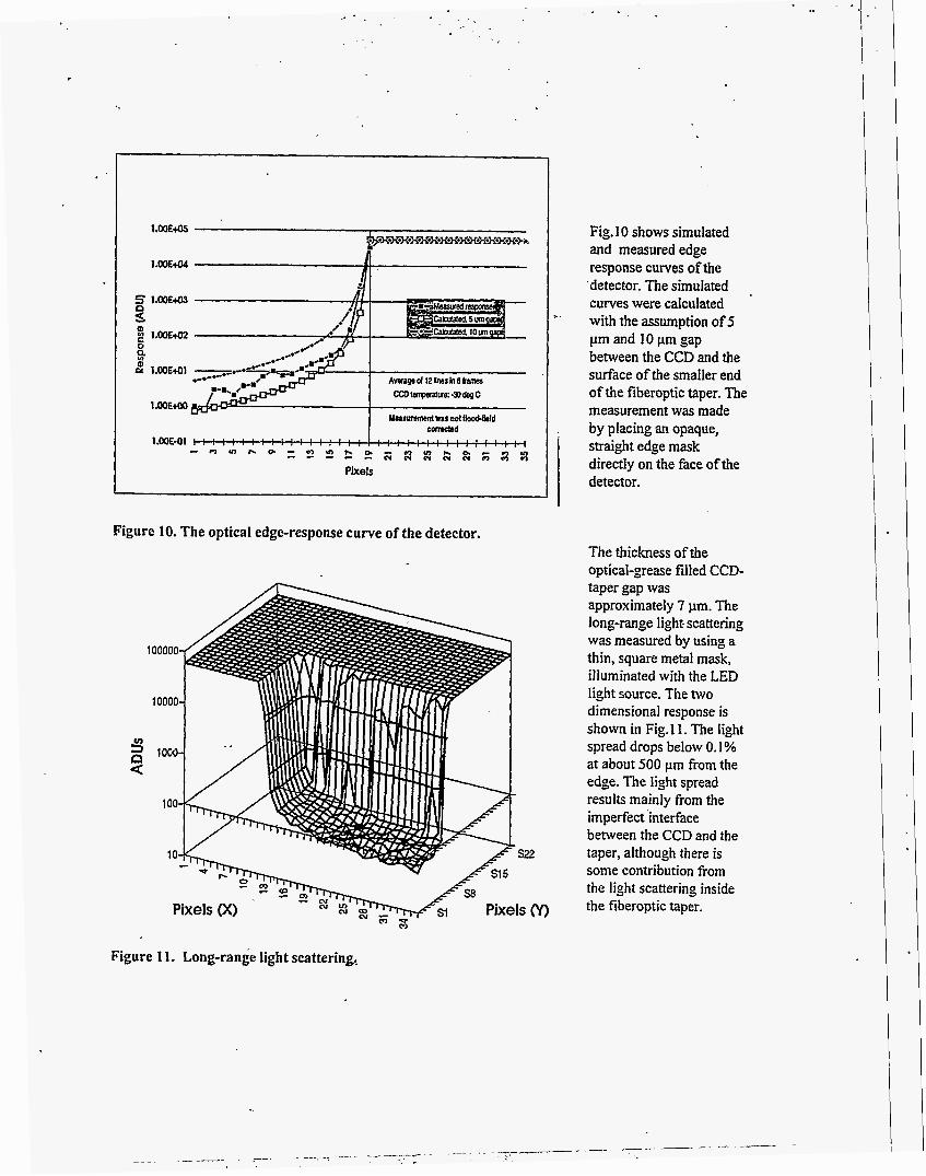
straight edge mask directIy on the face of the detector.
1.WEtOs
1.00E+04 n nl I
Figure 10. The optical edge-response curve of the detector. The thickness of the optical-grease filled CCD- taper gap was approximately 7 pm. The long-range light. scattering was measured by using a thin, square metal mask, illuminated with the LED light source. The two dimensional response is shown in Fig.11. The light spread drops below 0. I % at about 500 pm from the edge. The light spread results mainly from the imperfect 'interface between the CCD and the taper, although there is some contribution from the light scattering inside the fiberoptic taper.

PPhdedze=50un
CCDl~nperabrre =30 degc Noloodfeldmreclia-6
Average d 6 frames
Figure 12. Optical spot-profile of the detector.
Fig.12 shows the profile of the measured point spread function curve of the detector. The width of the curve is approximately 120 pm at IO%, 180 pm at l%.and 280 pm at 0.1%, measured with the 50 pm pinhole.
The CCD transfer function was measured on all 18 sections of the detector. One of these curves is shown in Fig.13. The dark current of all CCDs were also measured and compared with the '
measured values supplied by the manufacturer. .
0.01 0.1 1 10 ' 1w
Signal level (100% = Full scale)
Figure 13. CCD transfer curve.
The stability of the positioning of the CCD's is essential for the reliable geometrical distortion correction. The stability has been measured by mounting a 50 pm pinhole on the detector surface and imaging the resulted peak in different orientations of the detector head. The measurement was repeated after several thermal cycles. The position of the peak shifted less then 7 pm (0.1 pixel) during these tests.

4.3. X-ray tests.
After coating of the detector face with the X-ray converter phosphor, the X-ray tests of the APS-I detector system were conducted usingboth a rotating anode X-ray generator source (monochromatic or wide bandwidth), and monochromatic X-rays at the Advanced Photon Source. The tests at the rotating anode source were made by 8keV X-rays, except the flood field tests, where a non-monochromatic X-ray beam was used (copper target). The X-ray energy was 12.5 keV at the measurements made at the APS. The following X-ray tests have been completed to date:
e* Uniformity tests X-ray spatial resolution measurements Conversion gain measurements (at 12.5 keV)
Further X-ray tests are planned at different X-ray energies between 8 keV and 20 keV.
pinhole she: 50 x 50 um Eqmsuretme 12s Energy I 12.5 kaV
Pixels (1 pixel = 70 urn)
The X-ray spatial resolution was measured by imaging a 50 pm x 50 pm X-ray pinhole, placed in a collimated, mono-energetic X-ray beam at Beamline 19ID. The intensity of the direct beam was attenuated by a silicon reflector, where the reflection angle was set to be larger then the critical angle'. This method gives a harmonic-free . attenuated X-ray beam. The X-ray spatial resolution ofthe detector is significantly lower then the optical resolution due to light scattering in the phosphor layer. The response curve is shown in Fig. 14. Further studies are planned to improve the point-spread behavior of the detector.
Figure 14. X-ray spot profile.
4.4. Protein Crystallography tests.
Several data sets have been collected by the APS-I detector system at Beamline ID 19 at the Advanced Photon Source. The collected data were analyzed by D*Trek software package. The crystallographic results proved that the detector system performs according to the original design specification of the system. As an example, diffraction image of a Fragile Histidine Triad protein (FHIT) crystal" is shown in Fig.15a and Fig.lSb. The image was taken by the APS-I detector in a 1 second exposure. Fig.15a shows the full image, Fig. 15b is a magnified portion of the.same image, showing the separated Bragg peaks.

_..
. .. ,
Figure 15a. A diffraction image of a FHIT protein crystal, taken by the ApS-1 detector.
Figure 15b. Magnified view of the same diffraction image.

5. CONCLUSION
A nine module, large area (210 x210 mm'), high resolution (3,072 x 3,072 pixel) fiberoptic taper / CCD detector was presented. The detector has been installed at the Structural Biology Center's 191D beamline of the Advanced Photon Source in the Argonne National Laboratory. The detector system performs according to its design specifications, producing high quality data in protein crystallography measurements. This type of detector could be used in any other X-ray imaging, or visible-light contact-imaging applications, where large area, high spatial resolution and wide dynamic range are required.
6. ACKNOWLEDGEMENTS
The authors gratefully acknowledge all those who have participated in the design, development, construction and tests of the APS-1 detector project. This work was supported by contract W23I-ENG-38 from the U.S. Department of Energy, Ofice of Health and Environmental Research.
7. REFERENCES
1. Stout, G.H. and Jensen, L.H.: "X-ray Structure Determination", Wiley & Sons, N.Y. (1991) 2. Amdt, U.W. and Wonacott, A.J.: "The Rotation Method in Crystallography", ElsevierNorth
3. Winnick, H. and Doniach, S.: "Synchrotron Radiation Research", Plenum Press, N.Y. (1980) 4. Stanton, M.: Nuclear Instruments and Methods, A325, pp.550-557, (1993) 5. Stanton, M., Phillips, W.C., O'Mara, D., Naday, I.: Nuclear Instruments and Methods, A325,
6. Stanton, M., Phillips, W.C., Li, Y., Kalata, K.: Journal ofApplied Ctystallography, 25,
7. Naday. I., Ross, S., Kanyo. M., Westbrook, M.L., Westbrook, E.M., Phillips, W.C., Stanton, M.:
8. Tate, M.W., Eikenberry, E.F., Barna, S.L., Walli M.E., Lowrance, J.L., Gruner, S.M.: Journal of
9. Lima, C.D, D'Amico, K.L., Klein, M.G., Naday, I., Rosenbaum, G., Westbrook, E.M.,
10. Brown, G. and Moncton, D.E.: Handbook on Synchrotron Radiation, Vo1.3, Elsevier Science
Holland, Amsterdam, (1 977)
pp.558-567, (1993)
pp.549-558, (1992)
Proc. Soc. Photo-Opt. Instr. Eng., Vol. 2415, pp. 236-249, (1995)
Applied Crystallography, 28, pp. 196-205, (1995)
Hendrickson, W.A.: Structural and Biochemical Analysis of Human FHIT. To be published:
Publisher B.V. (1991)
DISCLAIMER
This report was prepared as an account of work sponsored by an agency of the United States Government. Neither the United States Government nor any agency thereof, nor any of their employees, makes any warranty, express or implied, or assumes any legal liability or responsi- bility for the accuracy, completeness, or usefulness of any information, apparatus, product, or process disclosed, or represents that its use would not infringe privately owned rights. Refer- ence herein to any specific commercial product, process, or service by trade name, trademark, manufacturer, or otherwise does not necessarily constitute or imply its endorsement, recom- mendation, or favoring by the United States Government or any agency thereof. The views and opinions of authors expressed herein do not necessarily state or reflect those of the United States Government or any agency thereof.