chemical mechanical polishing (cmp) metrology with …€¦ · chemical mechanical polishing (cmp)...
TRANSCRIPT

Chemical Mechanical Polishing (CMP)Metrology with AdvancedSurface Profiler
>>>Figure 1. The key matrices of metal chemical mechanical polishing of W or Cu.
>>>Figure 2. (Left) Currently the CMP process requires the resolution specification beyond optical and stylus profilers, and it can be only met by atomic surface profiler.
Chemical Mechanical PolishingDuring the metal Chemical Mechanical Polishing (CMP), the levels of metals (Cu or W) and oxides are reduced, causing surface irregularities. Both line width and pattern density (e.g., line density) in-fluence yield and contribute to the surface variation. The CMP process must be optimized to achieve the best planarity (i.e., flat surface) while improving yield. Erosion reflects the localized loss of oxide level while dishing accounts for the change in metal level when either Cu or W recedes or protrudes above the oxide level, as shown in Figure 1. Dishing and erosion account for a major portion of yield losses and are the critical factors in the CMP process.
The key matrices for CMP performance are Total Cu Loss (TCL),
TCL = Oxide Loss + Erosion + Dishing
which is the sum of copper losses from field oxide loss, erosion, and dishing. Out of these three, as shown in Figure 2, field oxide loss can be measured by optical method, and erosion and dishing by profilometry. However, conventional stylus and optical profilers can only resolve features down to 0.5 µm ~1 µm. With the continuous reduction in the minimum feature size in CMP, both the stylus and the optical profiler fail to meet the required specifications for accurate dishing and erosion measurement. Optical profilers are limited by their spot size and inability to distinguish which side of a given region is higher. Also, stylus profilers make destructive contact with real devices, making them ineffective for in-line tool on active regions. The Atomic Force Microscope (AFM) based profiler constitutes the practical solution to monitor and reduce the dishingand erosion
>>>Figure 3. (Right) The XE-Wafer is a completely automated AFM Surface Profiler system for semiconductor metrology of 200/300 mm wafers.
�

2
XE-Wafer, Advanced AFMSurface Profiler Atomic Force Microscopy (AFM) is emerging as an essential tool in the semiconductor industry to character-ize the results of processing such as the overall dishing or wash-out of the feed-through fields by CMP. Recess data from an AFM is superior to those from a stylus or a optical profiler. The main bottleneck of previous AFMs employed as CMP tool monitors has been the sam-pling plan limited by the throughput of the AFM. A higher-throughput AFM is greatly desired to enable the option of denser sampling for development of future nodes, and for in-line monitor-ing of those nodes with higher sampling frequency, as the devices enter produc-tion.
With Long Range Profilers (LRP) easily meeting the scan range requirements for semiconductor pro-cessing, the XE-Wafer provides the state-of-the-art linear translation capability with minimal vertical deviation of less than ±10 nm from the reference plane over a 10 mm profiling distance.The LRP is built into the ultra flat vacuum wafer chuck. The scanning mechanism translates the wafer chuck relative to the AFM probe, and causes essentially no degradation of AFM measurement, and has minimal impact on the system’s physical configuration. In addition, the Z-scanner of the XE-Wafer is completely decoupled from the XY scanner to effectively eliminate the cross-talk and non-linearity problems that are intrinsic to conventional piezoelectric tube based AFMs. Moreover, the high performance Z-servo can image the detailed nano-metrological features with unprecedented repeatability and reliability.
Post-CMP Profiling of Edge-Over-Erosion (EOE)Recently, some additional complexity in metal CMP profiling has surfaced: EOE. EOE appears to be a phenomenon of mostly very fine metal line and array lines (line width ≤ 0.5 µm). Some difficulties in investigating this phenomenon using commercially available surface profilers have been observed due to its repeatability problems. In this report, the EOE phenomena have been systematically investigated using XE-Wafer.
SKW6-5 Cu/TEOS patterned wafers shown in Figure 4 were used for the study. The test wafers were patterned for 90 nm technology node, and its minimum feature size was 0.12 µm. Different line width features were used from 0.12 µm to 0.5 µm with various pattern densities up to 90%. The electro-chemical deposition Cu layer thickness was 5,700 Å.
Post-CMP metrology issues for the current test wafers are illustrated in Figure 5 and include:
Erosion total = Erosion + EOE
Total Cu loss = Erosion total + Dishing + Oxide Loss
>>>Figure 4. SKW6-5 Cu/TEOS patterned wafer for 90 nm technology node.
>>>Figure 5. Post-CMP profiling of Erosion, EOE, and dishing by XE-CMP.
�

3
<<<Figure 6. Cu post-CMP profiling by XE-Wafer with different line width from 0.12 µm to 15 µm at 750 µm × 750 µm arrays with pattern density of 50%.
<<<Figure 7. Cu post-CMP profiling by XE-Wafer with different pattern density from 10% to 65% at 750 µm × 750 µm arrays with 0.25 µm line width.
If the metal and oxide levels are out of specification and are not detected properly during profiling, the consequences will not be seen until electrical tests. At this point, the device will be finished, with many other similar wafers already processed.
Figure 6 shows the images of Cu CMP profiling with different line widths (0.12~15 μm) at 750 × 750 μm arrays with pattern density of 50%. The levels of EOE, dishing, and the resultant total erosion change with different line widths. Note that the both edges of each trench are clearly and consistently profiled, indicating superb Z-servo performance to trace the steep walls of the trench edges without hitting or sticking to the sample. Only with properly defined edges, one can make confident metro-logical measurements of post-CMP trenches. If the Z-servo is not fast enough, the trench profiles would be deformed along the edges, which has been the major problem with previous surface profilers with insufficient Z-servo bandwidth.
Figure 7 shows the images of Cu CMP profiling with different pattern densities (10~65%) at 750 × 750 μm arrays with 0.25 μm line width.
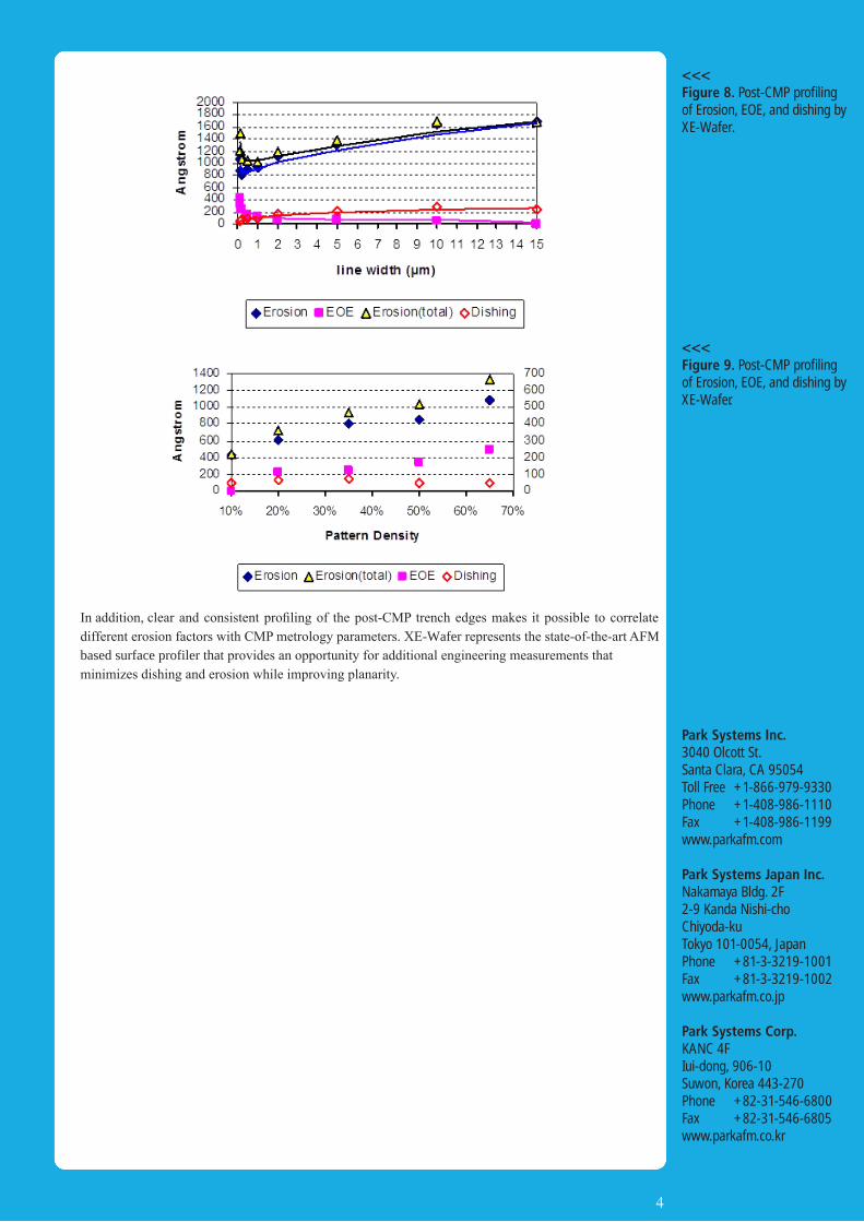
Figure 8 plots the key CMP metrology parameters, and one can clearly observe the correlation be-tween different erosion factors and the line width. Figure 9 plots the key CMP metrology parameters as a function of pattern density.
ConclusionThe new integrated intelligent XE-Wafer system was used to investigate metal CMP process “EOE”. Our data show that EOE is a function of feature size, array line shapes, and pattern density. The revolutionary design of the XE-Wafer allows for the unprecedented Z-servo performance, and achieves ten times the throughput of that of previously available surface profilers in the market.
�
Park Systems Inc.3040 Olcott St.Santa Clara, CA 95054 Toll Free +1-866-979-9330Phone +1-408-986-1110Fax +1-408-986-1199 www.parkafm.com
Park Systems Japan Inc.Nakamaya Bldg. 2F2-9 Kanda Nishi-choChiyoda-kuTokyo 101-0054, JapanPhone +81-3-3219-1001Fax +81-3-3219-1002www.parkafm.co.jp
Park Systems Corp.KANC 4FIui-dong, 906-10Suwon, Korea 443-270Phone +82-31-546-6800Fax +82-31-546-6805www.parkafm.co.kr
<<<Figure 8. Post-CMP profiling of Erosion, EOE, and dishing by XE-Wafer.
In addition, clear and consistent profiling of the post-CMP trench edges makes it possible to correlate different erosion factors with CMP metrology parameters. XE-Wafer represents the state-of-the-art AFM based surface profiler that provides an opportunity for additional engineering measurements that minimizes dishing and erosion while improving planarity.
<<<Figure 9. Post-CMP profiling of Erosion, EOE, and dishing by XE-Wafer.
�