chemical vapor deposition of metastable germanium … · chemical vapor deposition of metastable...
TRANSCRIPT

Chemical Vapor Deposition of Metastable Germanium Based Semiconductors for
Optoelectronic Applications
by
Charutha Lasitha Senaratne
A Dissertation Presented in Partial Fulfillment
of the Requirements for the Degree
Doctor of Philosophy
Approved July 2016 by the
Graduate Supervisory Committee:
John Kouvetakis, Chair
Andrew Chizmeshya
José Menéndez
ARIZONA STATE UNIVERSITY
August 2016

i
ABSTRACT
Optoelectronic and microelectronic applications of germanium-based materials have
received considerable research interest in recent years. A novel method for Ge on Si
heteroepitaxy required for such applications was developed via molecular epitaxy of
Ge5H12. Next, As(GeH3)3, As(SiH3)3, SbD3, S(GeH3)2 and S(SiH3)2 molecular sources
were utilized in degenerate n-type doping of Ge. The epitaxial Ge films produced in this
work incorporate donor atoms at concentrations above the thermodynamic equilibrium
limits. The donors are nearly fully activated, and led to films with lowest resistivity values
thus far reported.
Band engineering of Ge was achieved by alloying with Sn. Epitaxy of the alloy layers was
conducted on virtual Ge substrates, and made use of the germanium hydrides Ge2H6 and
Ge3H8, and the Sn source SnD4. These films exhibit stronger emission than equivalent
material deposited directly on Si, and the contributions from the direct and indirect edges
can be separated. The indirect-direct crossover composition for Ge1-ySny alloys was
determined by photoluminescence (PL). By n-type doping of the Ge1-ySny alloys via
P(GeH3)3, P(SiH3)3 and As(SiH3)3, it was possible to enhance photoexcited emission by
more than an order-of-magnitude.
The above techniques for deposition of direct gap Ge1-ySny alloys and doping of Ge were
combined with p-type doping methods for Ge1-ySny using B2H6 to fabricate pin
heterostructure diodes with active layer compositions up to y=0.137. These represent the
first direct gap light emitting diodes made from group IV materials. The effect of the single
defected n-i interface in a n-Ge/i-Ge1-ySny/p-Ge1-zSnz architecture on electroluminescence

ii
(EL) was studied. This led to lattice engineering of the n-type contact layer to produce
diodes of n-Ge1-xSnx/i-Ge1-ySny/p-Ge1-zSnz architecture which are devoid of interface
defects and therefore exhibit more efficient EL than the previous design. Finally, n-Ge1-
ySny/p-Ge1-zSnz pn junction devices were synthesized with varying composition and doping
parameters to investigate the effect of these properties on EL.

iii
ACKNOWLEDGMENTS
I would chiefly like to thank my advisor, Prof. John Kouvetakis, without whose guidance,
instruction and enthusiasm this work would not have been possible. Similarly, the
knowledge and support provided by my committee members Prof. José Menéndez and
Prof. Andrew Chizmeshya was essential in bringing this effort to completion.
I would also like offer my gratitude to Dr. Gordon Grzybowski and Dr. Richard Beeler for
the training they provided at the initial stages of this research. The collaborative effort of
my colleagues Dr. Chi Xu, Dr. James Gallagher, Patrick Sims, Dr. Liying Jiang, Ruben
Favaro, and Patrick Wallace contributed directly and indirectly to many components of this
research, and I am sincerely grateful for their support.
Many facilities provided by the LeRoy Eyring Center for Solid State Science at Arizona
State University were essential for this research. I would like to especially thank Barry
Wilkens for assistance with ion beam analysis, and Prof. Lynda Williams for providing
SIMS training. The John M. Cowley Center for High Resolution Electron Microscopy and
Ira A. Fulton Center for Solid State Electronics Research also provided equipment and
instruments used in this work.
I am also grateful for the Air Force Office of Scientific Research for funding that enabled
this work.
Finally, I am forever grateful to my family who, though a world away, were a constant
source of support and strength throughout the demanding process of completing my
graduate studies.

iv
TABLE OF CONTENTS
Page
LIST OF TABLES ...............................................................................................................x
LIST OF FIGURES ........................................................................................................... xi
CHAPTER
1. INTRODUCTION AND BACKGROUND ....................................................................1
Introduction .............................................................................................................. 1
Germanium-tin ......................................................................................................... 2
Properties and Potential Applications ...............................................................2
History of Materials Synthesis and Elucidation of Fundamental Physical
Properties .......................................................................................................... 4
Progress in Device Implementation ..................................................................6
Outline of Current Work .......................................................................................... 8
Growth of High Sn Content Alloys on Ge Buffered Si Substrates ...................9
Measurement of Photoluminescence from GeSn Alloys ..................................9
Development of Low Temperature Hydride Chemistries for the Doping of Ge
and GeSn......................................................................................................... 10
Optical Devices from GeSn Alloys .................................................................10
Conclusion ……………………………………………………………………….11

v
CHAPTER ..................................................................................................................... Page
2. SYNTHESIS OF CVD PRECURSORS FOR DEPOSITION OF INTRINSIC AND
DOPED GE AND GESN .................................................................................................. 13
Introduction ............................................................................................................ 13
Synthesis of Trigermane and Tetragermane .......................................................... 13
Synthesis of Deuterostannane ................................................................................ 16
Synthesis of Trisilylphosphine, Trisilylarsine and Trisilylstibine ......................... 18
Synthesis of Trigermylphosphine .......................................................................... 20
Synthesis of Deuterostibine ................................................................................... 21
Synthesis of Disilylsulfide ..................................................................................... 22
Synthesis of Digermylsulfide ................................................................................. 23
Synthesis of Diborane ............................................................................................ 24
3. HIGH-ORDER GE-HYDRIDE CHEMISTRY FOR LOW TEMPERATURE GE
BASED MATERIALS FABRICATION: A STUDY OF PENTAGERMANE .............. 26
Introduction ............................................................................................................ 26
Thermochemistry Simulations ............................................................................... 30
Simulation of Vibrational Properties ..................................................................... 35
Reaction Thermodynamics of Higher Order Ge-Hydrides .................................... 37
GenH2n+2 Yield Optimization ................................................................................. 44

vi
CHAPTER Page
Ge-on-Si Growth Studies via Pentagermane ......................................................... 47
Conclusion …………………………………………………………………...…. 49
4. EPITAXIAL GE ON SI FILMS DEGENERATELY N-TYPE DOPED WITH AS, SB
AND S THROUGH LOW TEMPERATURE DEPOSITION TECHNIQUES UTILIZING
HIGH REACTIVITY PRECURSORS ............................................................................. 52
Introduction ............................................................................................................ 53
In-Situ Low Temperature As Doping of Ge Films Using Trisilylarsine and
Trigermylarsine ...................................................................................................... 55
Introduction .....................................................................................................55
Deposition Procedure for Ge:As Films ...........................................................59
Determination of Structural Properties and Donor Incorporation Levels .......60
Donor Activation Studies ................................................................................67
Electrical Properties ........................................................................................69
Antimony Doping of Ge Using SbD3 .................................................................... 71
Introduction .....................................................................................................71
Deposition Procedure ......................................................................................73
Determination of Sb Concentrations and Structural Characterization ............74
Electrical Properties of Ge:Sb Films – Carrier Concentration ........................82
Electrical Properties of Ge:Sb Films – Resistivity ..........................................83

vii
CHAPTER Page
Doping Efficiency ...........................................................................................85
Sulfur doping of Ge using Disilylsulfide and Digermylsulfide ............................. 87
Introduction .....................................................................................................87
Growth of Ge:S layers on Si(100) using Digermylsulfide and Tetragermane 90
Growth of Ge:S Using Disilylsulfide ..............................................................95
Conclusion ........................................................................................................... 101
5. GROWTH OF GERMANIUM-TIN ALLOYS ON GE BUFFERED SI SUBSTRATES
......................................................................................................................................... 104
Introduction .......................................................................................................... 104
Ge buffered Si Substrates – Significance and Fabrication Methods ................... 106
Growth of GeSn Alloys Using Ge2H6 and SnD4 Precursors ............................... 108
Growth of GeSn Alloys Using Ge3H8 and SnD4 Precursors ............................... 112
Microstructure of GeSn Alloys Grown on Ge/Si Substrates ............................... 116
Quantification of Defect Density and Modeling Strain Relaxation Behavior of
Ge1-ySny/Ge Alloys ............................................................................................... 124
Conclusion ........................................................................................................... 133
6. PHOTOLUMINESCENCE STUDIES OF GESN ALLOYS AND EMISSION
ENHANCEMENT VIA N-TYPE DOPING .................................................................. 136
Introduction .......................................................................................................... 136

viii
CHAPTER .............................................................................................................. Page
Determination of Indirect-Direct Crossover in Intrinsic GeSn Alloys ................ 139
Growth of n-doped Ge1-ySny Alloys (y=0.04-0.09) Using P(GeH3)3 as the Doping
Agent ………………………………………………………………………….. 145
Materials Properties of P Doped GeSn Samples ................................................. 146
Photoluminescence Measurements and Band Gap Determination of n-type doped
films…………………………………………………………………………… 152
Group V Silyl Compounds for Doping of GeSn Alloys ...................................... 156
Trisilylphosphine Source ...............................................................................156
Trisilylarsine Source ......................................................................................158
Summary and Conclusions .................................................................................. 161
7. GROWTH OF GESN BASED DIODE STRUCTURES AND ENHANCING DEVICE
PERFORMANCE BY REGULATION OF MICROSTRUCTURE .............................. 163
Introduction .......................................................................................................... 164
Device Design: n-Ge/i-Ge1-ySny/p-Ge1-zSnz Diodes ............................................. 170
Buffer Layer Growth .....................................................................................171
Growth of Active Ge1-ySny Layers (y=0.02-0.137) .......................................172
Growth of p-type Doped Ge1-zSnz Capping Layers .......................................174
Materials Properties of n-Ge/i-Ge1-ySny/p-Ge1-zSnz Device Stacks ...............175
Microstructure of n-Ge/i-Ge1-ySny/p-Ge1-zSnz Device Stacks ........................178

ix
CHAPTER ..................................................................................................................... Page
Device Fabrication and Diode Behavior .......................................................182
Electroluminescence Performance of n-Ge/i-Ge1-ySny/p-Ge1-zSnz Devices .. 185
Eliminating Interface Defects: n-Ge1-xSnx/i-Ge1-ySny/p-Ge1-zSnz Diodes ............ 189
Growth of pn Diode Structures ............................................................................ 195
Conclusion ........................................................................................................... 204
REFERENCES ................................................................................................................206
APPENDIX
A EXPERIMENTAL PARAMETERS FOR DEPOSITION OF GE1-YSNY
ALLOYS ON GE/SI SUBSTRATES .............................................................. 221
B PERMISSIONS FOR REPRINTED MATERIALS ......................................241

x
LIST OF TABLES
Table .............................................................................................................................. Page
1 – FTIR Spectra of P(SiH3)3, As(SiH3)3 and Sb(SiH3)3 .................................................. 20
2 - Summary of Structural and Energetic Results for Isomers of Pentagermane. ............ 32
3 - Thermochemistry Data for the Pentagermane Isomers ............................................... 33
4 - Isomer Admixtures of Pentagermane Used to Generate the Theoretical Spectra. ...... 43
5 - Dependence of Equilibrium GenH2n+2 Hydride Yields at 600 K (~ 327°C) as a Function
of the Initial Mixture of GeH4, Ge2H6 and Ge3H8. ........................................................... 45
6 – Growth Parameters and Compositions of As Doped Ge Films Using As(SiH3)3 ....... 61
7 – Growth Parameters and Compositions of As doped Ge Films Using As(GeH3)3 ...... 65
8 – Absolute Sb Concentrations and Carrier Concentrations in Ge:Sb Films Deposited On
Ge and GeSi Buffers. ........................................................................................................ 74
9 - Summary of S-doped Ge Film Parameters Produced Using S(GeH3)2 . ..................... 91
10 - Summary of S-doped Ge Film Parameters Produced Using S(GeH3)2. .................... 95
11 – Thickness, Composition and Doping of the n and p Layers of n-Ge1-ySny/p-Ge1-zSnz
Diode Stacks. .................................................................................................................. 199

xi
LIST OF FIGURES
Figure ............................................................................................................................. Page
1 – FTIR Spectra of Ge3H8 and Ge4H10 ............................................................................ 15
2 – FTIR Spectrum of SnD4. ............................................................................................. 18
3 - 1H NMR Spectrum of S(SiH3)2 in CDCl3 Solvent ...................................................... 23
4 - 1H NMR Spectrum of S(GeH3)2 in CDCl3 Solvent ..................................................... 25
5 - Summary of Simulated Infrared Spectra for the Ge5H12 Isomers in the Low-Frequency
and High-Frequency Regimes........................................................................................... 36
6 - Temperature Dependence of the Reaction Free Energies for Pentagermane Production
........................................................................................................................................... 40
7 - Temperature Dependence of the Equilibrium Concentrations for the Reaction System
Producing Pentagermane .................................................................................................. 41
8 - Experimental and Theoretical Infrared Spectra of Liquid and Gas Phases of Ge4H10 and
Ge5H12. .............................................................................................................................. 42
9 - XTEM Image of Ge on Si Film Showing the Typical Microstructure Observed Within
the Field of View, and XRD On and Off Axis Plots of RTA Processed Sample Indicating
a Significant Level of Tensile Strain. ............................................................................... 49
10 - SIMS Depth Profile of n-Ge Sample Grown Using As(SiH3)3. ................................ 60
11 - XTEM Micrograph and AFM image of Sample Doped With As(SiH3)3 at 330°C ... 63
12 - SIMS Depth Profile of Ge Structure Grown by As(GeH3)3 ...................................... 65
13 - XRD (004) Peaks for As doped Ge Samples With Doping Levels of 2.5×10¹⁹
cm-3 and 7.8×1019 cm-3. ..................................................................................................... 66
xii
Figure Page
14 - Resistivity of Ge Films Doped With As Using the As(MH3)3 (M = Si, Ge) Precursors.
........................................................................................................................................... 70
15 - RBS Spectra and Composition Fit for a Sample Containing 9.2x1019 cm-3 Carrier
Concentration.. .................................................................................................................. 75
16 – SIMS Elemental Profiles for a Sample Grown on Sb Doped Ge ............................ 77
17 – XTEM and AFM Images of a Ge:Sb Film................................................................ 78
18 - θ-2θ Scans for the 004 Reflection in Several Sb-doped Ge Films Grown on Ge0.95Si0.05.
........................................................................................................................................... 79
19 – Plot of the Experimental Relaxed Lattice Parameter Determined From (224) RSMs
vs. the Total Sb Content Determined From RBS.. ............................................................ 81
20 - Experimental Carrier Concentrations n as a Function of the Measured Donor
Concentrations Nd in Ge:Sb Films. ................................................................................... 83
21 – The Resistivity Values From Ge:Sb films Doped With SbD3 Compared With Bulk
Data. .................................................................................................................................. 84
22 – Efficiency of Doping for P, As, and Sb Doped Ge Films Synthesized Using Single
Source CVD Method......................................................................................................... 86
23 - XTEM Micrograph of S Doped Ge Layer Grown Upon Si(100) at 380oC Via Reactions
of S(GeH3)2 and Ge4H10. ................................................................................................... 92
24 - XTEM micrograph of 800 nm thick Ge/Si(100) sample doped with S and
corresponding RBS spectra and HRXRD plots ............................................................... 96
25 - SIMS elemental profile of the as-grown Ge:S sample. ............................................. 98

xiii
Figure Page
26 – 2 MeV RBS Random and Channeling Spectra for a 540 nm Thick Ge0.97Sn0.03 Film
and HRXRD Scans ......................................................................................................... 111
27 – RBS Random and Aligned Spectra for a Ge0.93Sn0.07/Ge/Si(100) Sample and
Corresponding XRD Reciprocal Space Maps................................................................. 113
28 – Growth Rates Observed for Varying Sn/Ge Atomic Ratios in the Precursor Mixtures
at Various Temperatures ................................................................................................. 115
29 – Growth Rates Obtained at 295°C Using Mixtures With Varying Concentrations of
Ge3H8. ............................................................................................................................. 116
30 – rfilm vs. rgas for Samples Grown Using Ge3H8 and SnD4 Spanning the y=0.05-0.11
Composition Range. ........................................................................................................ 117
31 – XTEM Micrograph of a 550 nm Thick Ge0.91Sn0.09 Film Grown on Ge Buffered Si
......................................................................................................................................... 118
32 - STEM/EELS Elemental Map and Concentration Plots of a Ge0.96Sn0.04/Ge Sample
......................................................................................................................................... 119
33 - EELS and STEM Images of a Ge0.96Sn0.04 Film ..................................................... 121
34 - XTEM High-Resolution Micrographs of a 700 nm Thick Ge0.94Sn0.04 Layer Grown
Upon Si Using a 1500 nm Thick Ge Buffer Layer ......................................................... 122
35 - Plan View TEM Image Shows Dislocations and Corrected FWHM of Several Bragg
Reflections for a Ge0.96Sn0.04 Sample .............................................................................. 126
36 - Relaxation Fraction R for As-Grown Ge1-ySny Films on Ge-Buffered Si. .............. 127
37 - Ge1-ySny Film Thicknesses Compared With Calculations of Critical Thickness for
Strain Relaxation. ............................................................................................................ 129

xiv
Figure Page
38 – (224) RSM of a 500 nm thick Ge0.94Sn0.06 Alloy Film Deposited on Ge(100) Substrate.
......................................................................................................................................... 132
39 – XTEM Micrograph of a Ge0.94Sn0.06 Film Fully Strained to the Ge Substrate. ...... 133
40 – AFM Image of a 5μm×5μm Area of an As-Deposited, Fully Strained Ge0.94Sn0.06/Ge
Film and the Surface of the Same Film After Strain Relaxation Induced by Thermal
Processing. ...................................................................................................................... 134
41 – Photoluminescence Spectra from a Ge1-ySny/Ge/Si and a Ge1-ySny/Si Counterpart With
Similar Sn-Concentration and Thickness........................................................................ 141
42 - Photoluminescence From Two Selected Ge1-ySny/Ge/Si Samples ......................... 142
43 - Room Temperature PL Plots vs. Sn Fraction for Ge1-ySny (y = 0.003- 0.09). ........ 143
44 - Energies of Direct Gaps and Indirect Gaps vs. Sn Concentration for Ge1-ySny Alloys
With 0<y<0.11. ............................................................................................................... 145
45 – 224 Reciprocal Space Maps and AFM Image of a Ge0.94Sn0.06/Ge Sample. .......... 148
46 - XTEM Micrograph of n-type Ge0.936Sn0.064 Film Grown Upon a Ge Buffered Si
Substrate at 315°C. ......................................................................................................... 149
47 - STEM Images of the n-type Ge0.936Sn0.064 Film Grown on Ge Showing Defect Types
Present in This Sample.................................................................................................... 150
48 - STEM and Element Selective EELS Mapping Show Random Sn Substitution in
Diamond Lattice.............................................................................................................. 151
49 – PL Plots of Intrinsic and Phosphorus Doped 6 % Sn Alloy Showing the Optimized
the Emission Intensity in the Doped Ge0.94Sn0.06 Alloy. . .............................................. 153
xv
Figure Page
50 - Normalized PL Spectra of n-type Ge1-ySny (n~1-3x1019 cm-3) Samples with y= 0.04,
0.07 and 0.09 Recorded at Room Temperature Using a PbS Detector. .......................... 154
51 - Direct and Indirect Band Gaps Extracted From Fits of the PL Spectra of Phosphorus
Doped Alloys.. ................................................................................................................ 155
52 – Elemental Profiles of Ge, P, Si and Sn Obtained From a 400 nm Thick Ge0.95Sn0.05
Alloy Film Deposited on Ge/Si(100). ............................................................................. 157
53 - Room Temperature PL Spectra of n-type Ge0.96Si0.04 Grown by P(GeH3)3 and
As(SiH3)3. ........................................................................................................................ 159
54 – Schematic of n-Ge/i-Ge1-ySny/p-Ge1-zSnz Device Depicting the Active Layer
Deposited on n-doped Ge and Capped by a p-type Doped GeSn Layer ......................... 167
55 – Device Schematic for the n-Ge1-xSnx/i-Ge1-ySny/p-Ge1-zSnz Architecture ............... 168
56 – Schematic of p-Ge1-zSnz/n-Ge1-ySny LED ................................................................ 170
57 – RBS Spectrum of a n-Ge/i-Ge0.863Sn0.137/p-Ge0.92Sn0.08 Device. ............................ 176
58 – The (224) RSM of a n-Ge/i-Ge0.87Sn0.13/p-Ge0.90Sn0.10 Device Structure ............... 177
59 - XTEM Image and (224) RSM of Ge/ Ge0.98Sn0.02 Film .......................................... 178
60 – High Resolution STEM BF Images of Ge/i-Ge0.895Sn0.105 and Ge/i-Ge0.915Sn0.085
Interfaces ......................................................................................................................... 180
61 - XTEM Images of the Interface Microstructure of a Ge0.93Sn0.07 Device. ............... 181
62 – XSTEM Images of a p-i-n Heterostructure Device Comprised of an n-Ge Bottom
Contact, i-Ge0.863Sn0.137 Active Layer and p-Ge0.92Sn0.08 Top Contact ........................... 182
63 – IV Plots of n-Ge/i-Ge1-ySny/p-Ge1-zSnz Devices ..................................................... 183
64 – Activation Energies of Dark Currents at 0.2 V for Devices With y=0-0.11 ........... 184

xvi
Figure Page
65 – Current Dependence of the EL Spectra in the 0.1 – 0.5 A Range for Devices With
2.0% Sn and 7.0% Sn Active Layer Sn Compositions. .................................................. 186
66 – EMG Fits to EL Spectra Obtained From a Series of Devices With Active Layers in
the Composition Range y=0-0.12. .................................................................................. 187
67 - Schematic of Device Prototypes Comprising pin Layers With No Strain Relaxation at
the Device Interfaces, and SIMS Elemental Profiles of Such a Device ......................... 191
68 – Comparison of EL Intensity of n-Ge0.94Sn0.06/i-Ge0.93Sn0.07/p-Ge0.94Sn0.06 Diode
Design With Intensities Obtained From n-Ge/i-Ge1-ySny/p-Ge1-zSnz Diodes ................. 193
69 – XTEM Micrograph of n-Ge/n-Ge0.89Sn0.11/i-Ge0.85Sn0.15/p-Ge0.85Sn0.15 Device Stack
and IV plots of the 15% and 16% Sn Devices. ............................................................... 195
70 –XSTEM BF Image and (224) RSM of n-Ge0.907Sn0.093/p-Ge0.914Sn0.086 Diode Structure
Deposited on Ge/Si(100) Substrate. ................................................................................ 197
71 – Elemental Profiles of Ge, Sn, B, P and Si Obtained From SIMS for a n-Ge0.88Sn0.12/p-
Ge0.88Sn0.12 Diode Structure. ........................................................................................... 198
72 –Room Temperature EL Spectra From Sample pn Diodes Exibiting Superlinear Current
Dependence ..................................................................................................................... 200
73 – Schematic and EL Spectrum of a pn Diode Showing Two Color Emission .......... 201
74 – Room Temperature EL Spectrum of pn Diode Collected Using a PbS Detector in
Order to Resolve the Full Peak ....................................................................................... 202
75 – Differential Current vs. Applied Bias for Representative pn Diodes ..................... 203

1
CHAPTER ONE
Introduction and Background
1. Introduction
The microelectronics revolution has had a massive effect on modern society. Technologies
developed in the past 60-70 year have dramatically changed the way we interact with each
other, and the way we interact with our environment. Innovations in this field have been
dependent on the ability to manipulate various types of semiconductor materials that have
come to be used in modern electronic devices. Despite the wide range of materials that can
be used, one in particular has come to dominate mainstream electronic technology due to
its abundance, ease of use, and suitable physical, chemical, and electronic properties. This
material is Si, which forms the basis for manufacturing a vast majority of the commercially
available electronic devices.
Si based technologies have long been able to achieve exponential performance gains with
time, as exemplified by Moore’s law.1,2 This has been a result of technology advances that
enabled rapid miniaturization of transistor sizes. However the latest generation of Si
devices are fast approaching the physical limits of device scaling. Therefore, various
techniques have been successfully investigated to maintain increase in device performance
while circumventing the need for smaller devices. Examples include the use of strained Si3
and high dielectrics.4
A novel aspect of this drive for higher performance is the use of alternate semiconductor
materials in device fabrication. One of the ‘new’ materials which has been widely studied
for this purpose is Ge.5 While the use of Ge as a semiconductor predates the use of Si -with

2
the first transistor6 and integrated circuit7 being made using Ge- it was eventually replaced
with Si due to the latter material’s more favorable properties. However, the ability to use
Ge in combination with Si for strain engineering, as well as the superior carrier mobilities
and optical properties of Ge, have resulted in a resurgence of interest in Ge based materials
in microelectronics. An example is the use of silicon-germanium alloys for fabricating
devices containing strained Si.3 In the photonics arena, Ge on Si photodetectors have
become common in recent years.8 Another potential application area for Ge is in Si
integrated lasers.9 Lasing from Ge has been experimentally demonstrated,10,11 but these
devices require high threshold currents, and utilize complementary metal-oxide-
semiconductor (CMOS) incompatible fabrication methods which employ high
temperatures to induce tensile strain in the Ge active material. Due to such drawbacks,
significant improvements are necessary before they can be used in practical applications.
In order to obtain the desired optical properties for lasing and to expand the ability to
manipulate strain to enhance device performance, next generation optoelectronic and
electronic devices require greater flexibility in band gap and lattice engineering than can
be obtained only from the combination of Si and Ge. In this context, germanium-tin (GeSn)
alloys have been receiving increasing interest as a means of extending the capabilities of
the group IV semiconductor system. The state-of-the-art for this materials system prior to
the contributions arising from the work described in this thesis is briefly described below.
2. Germanium-tin
2.1. Properties and Potential Applications
Substitution of Sn atoms in place of Ge in the elemental Ge matrix will give the GeSn alloy
which shares with Ge the diamond cubic crystal structure. The Ge rich alloy is only

3
thermodynamically stable up to Sn content of 1.1%, with the maximum solubility being
observed at around 400°C.12 In the compositionally opposite extreme, the solubility of Ge
in Sn is even less, at 0.6%.12 Furthermore, the semiconducting diamond cubic structure of
Sn (α-Sn) is only stable up to 13°C.12 Therefore, thermodynamically stable combinations
represent only a small fraction of the composition space –and in turn optical and physical
properties– accessible with GeSn alloys. In consequence, it is not straightforward to use
this alloy system for expanding the properties of the group IV semiconductors, as is the
case for the fully miscible silicon-germanium (SiGe) alloys. However, theoretical
considerations have shown that GeSn alloys with metastable compositions will have
properties of great interest from the perspective of semiconductor device design.
The first and most intuitive property is the change of the lattice constant. The α-Sn allotrope
has a lattice constant of 6.4892 Å,13 compared to the 5.6571 Å of Ge.14 It is therefore
possible to achieve materials with lattice constants between these two extremes by an
alloying process. One technological significance of such materials lies in the fact that they
can be used as stressors for Ge channel material in device applications. The use of SiGe
for creating strained Si sets a precedent for this type of process. Applying tensile strain to
Si in transistors has paved the way for major increases in carrier mobility.3,15 Strained Ge
has the property of possessing even faster carrier transport capabilities. Furthermore, it has
been suggested that Ge alloyed with Sn has higher carrier mobilities than Ge itself, which
raises the possibility of fabricating transistors based on GeSn.16–19
The second aspect of GeSn alloys which is of technological interest is their use in bandgap
engineering of Ge. Two features of the change in band structure upon alloying with Sn are

4
of particular importance. Firstly the band gap is reduced, causing a redshift of the
wavelengths that can be used for emission and detection purposes.20,21 This in turn allows
the fabrication of GeSn based detectors that can cover the entire telecommunication
bandwidth and beyond, even into the mid-infrared region. Such detectors, being composed
of entirely group IV materials, can be integrated into existing Si platforms. At wavelength
of several microns, GeSn based devices become potential candidates for use in infrared
(IR) cameras and sensors which can be used for spectroscopic analyses. These may even
be combined with Si to fabricate lab-on-chip devices to be used in environmental
analysis.22 Secondly, upon alloying with Sn, the reduction of the direct gap located at the
point is greater than the reduction of the indirect gap at the L point, the latter being the
fundamental band gap of elemental Ge. Therefore, when sufficient amount of Sn is
incorporated into the Ge lattice, a direct gap semiconductor can be synthesized. The most
potent use of such a direct gap material would be the manufacture of lasers.23,24 A laser
made of GeSn can be directly integrated with prevalent Si microelectronics. Therefore it
would be a major milestone in achieving optical on-chip communication, leading the way
to faster and more energy efficient electronic devices.
2.2. History of Materials Synthesis and Elucidation of Fundamental Physical Properties
Due to the range of extremely beneficial applications, growth of GeSn alloys with Sn
compositions beyond the thermodynamic solubility limit has been a topic of interest to
researches for a number of years. The first experimental work with a bearing to this area
is the growth of α-Sn on InSb and CdTe substrates using molecular beam epitaxy (MBE)
during the 1980’s.25 This work showed that the problems posed by the thermodynamic
instability of the Sn allotrope of interest can be successfully circumvented by using growth

5
conditions which maintained low temperature, far from equilibrium conditions. At about
the same time, Goodman speculated on the possibility of obtaining direct gap materials
based on GeSn alloys.26 More detailed theoretical investigation of the band structure of
GeSn was later conducted by Jenkins and Dow.27 Shortly thereafter, successful
experimental synthesis of GeSn crystalline films using MBE techniques was demonstrated
by several authors.28–32
In subsequent work, the indirect and direct transition energies were determined
experimentally, and it was evident that the actual values deviate strongly from earlier
theoretical predictions.33 These results led to a more thorough investigation of the optical
properties of GeSn. Experimental studies were conducted by studying GeSn films using
Fourier transform infrared interferometry,34,35 spectroscopic ellipsometry,36
photoreflectance spectroscopy37 and photoluminescence spectroscopy.38–40 Theoretical
calculations based on density functional theory41,42 and empirical pseudopotential
methods43,44 agreed well with these experimental results, leading to an emerging consensus
in literature that the indirect-direct crossover composition for the Ge1-ySny alloy system (yc)
was in the range of y=0.06-0.13. This composition regime is much more amenable to
experimental realization than the earlier prediction of yc=0.20,27 and increased hope that
the practical demonstration of a direct gap group IV semiconductor material was within
reach.
Furthermore, the crystal quality of the films produced by the various techniques has also
improved overtime. Much of the early work mentioned above made use of MBE
techniques, and several groups have continued their development in recent years.38,45–48

6
However, greater progress has been achieved in synthesis of device quality GeSn materials
after the introduction of ultra-high vacuum chemical vapor deposition (UHV-CVD)
methods at Arizona State University (ASU).49,50 Several groups have since employed
different chemical vapor deposition (CVD) techniques such as atmospheric pressure CVD
(APCVD),51 reduced pressure CVD (RPCVD)52,53 and even metal organic CVD
(MOCVD)54 for the growth of GeSn alloys with great success, as will be discussed in
greater detail below. The major milestones achieved using both techniques have also been
summarized in recent reviews.55,56 Alternate deposition techniques such as solid phase
epitaxy57 and magnetron sputtering58 have also been investigated. Overall, tremendous
progress has been made in demonstrating the potential viability of this novel semiconductor
material in practical applications.
2.3. Progress in Device Implementation
Several researchers have investigated the possibility of using GeSn in advanced Ge p-
channel metal-oxide-semiconductor field-effect transistors (MOSFETs). One focus in this
area has been on using GeSn as source/drain stressors to impart compressive strain on the
active Ge channel. Proof-of-concept devices have been reported in literature, which
demonstrate the viability of this design concept.59,60 As an alternative method of using
GeSn alloys to obtain the same benefit, relaxed GeSn has been used as substrates to produce
tensile strained Ge epilayers.59 When used in devices, this material has increased hole and
electron mobilities, in contrast to the compressively strained case, where the mobility
enhancement is only observed for holes.

7
In addition to their use in stress implementation, GeSn alloys have themselves been used
as channel materials for MOSFETs. Increased carrier mobility resulting from the modified
band structure of the alloy in comparison to Ge results in improved performance, as has
been demonstrated for pMOSFETs fabricated using GeSn as channel material.17,51,61 In
addition, the reduced band gap offers additional pathway for using GeSn in next-generation
microelectronic devices, by increasing the band-to-band tunneling probability. This makes
GeSn a promising material for fabrication of tunneling field-effect transistors (TFETs),
which are being considered as an alternative to MOSFETs due to their superior power
efficiency. Several groups have demonstrated experimental TFETs fabricated from GeSn,
making this materials system a candidate worthy of consideration for practically
implementing TFET technology.62–64 Finally, research on interface engineering for gate
stack formation65,66 and metal contact formation to GeSn materials67 has also been ongoing.
In parallel with the development of GeSn based transistors, prototype light detection and
emission devices have also been developed by several groups. The first to report such a
device were Mathews and coworkers, who reported photoresponse from pin
heterostructure photodiodes fabricated on Si platforms.20 Electroluminescence (EL) from
devices with the same architecture were reported by Roucka et al.21 These results show the
feasibility of using this type of detector in the telecommunications arena for covering the
entire band range.20,68 While the reduction of band gap required for this purpose can be
achieved with an alloy with as little as 2% Sn, other applications such as IR sensors has
spurred the development of prototype devices incorporating increasing amounts of Sn,
which push the operable wavelengths further into the mid-IR region. MBE techniques have
been used by Kasper’s group to fabricate devices in which the active components have up

8
to 4% Sn.45,69,70 Tseng et al. have reported a light emitting diode (LED) comprising of
y=0.08 Ge1-ySny alloy, also grown using MBE techniques.48,71 More recently Du and
coworkers to demonstrated EL from a y=0.08 device grown using CVD techniques.72 All
of the above devices use a pin architecture in which the light emission occurs from an
intrinsic alloy sandwiched between p- and n- type doped Ge layers which act as electrical
contacts. Gupta et al. were the first to demonstrate EL from a pn device with a GeSn
component. In this case, emission was obtained from the p-GeSn layer which was deposited
on an n-Ge substrate which completed the device.73
3. Outline of Current Work
Many milestones in GeSn research were achieved at ASU. These include the
abovementioned demonstration of the first working GeSn LED,21 and measurement of
photoluminescence (PL) from GeSn alloy films grown directly on Si.74 The materials that
allowed these achievements were deposited Si(100) wafers using UHV-CVD techniques.
The key to the success of these methods was the use of a new class of precursors that are
highly reactive at low temperatures. The initial stage of development of these techniques
was first reported by Taraci et al. who used digermane (Ge2H6) as the precursor containing
Ge and phenyldeuterostannane (PhSnD3) for delivery of Sn.49 Bauer et al. subsequently
replaced the carbon containing PhSnD3 with the fully inorganic source deuterostannane
(SnD4).50 Higher reactivity Ge precursors in the form of trigermane (Ge3H8) and
tetragermane (Ge4H10) were introduced by Grzybowski et al. in order to further enhance
the low temperature compatibility of this method.75 While these methods have been
successful in producing a wide range of GeSn alloys suitable for optical studies and device
fabrication, obtaining highly crystalline material at and beyond the indirect-direct

9
composition proved challenging. One major limitation was the use of Si substrates. The
large lattice mismatch between the alloy and the substrate produces a high density of
defects, and the rapidly decreasing thermal stability of Ge1-ySny alloys as they near yc limits
the applicability of thermal treatments used on lower composition alloys to improve crystal
quality.
3.1. Growth of High Sn Content Alloys on Ge Buffered Si Substrates
In order to overcome this limitation, the work described in this thesis applied the above
UHV-CVD techniques for deposition of GeSn on Ge buffered Si substrates, also known as
virtual Ge substrates. Such substrates were first used for the growth of GeSn films because
they allow the integration of the alloys with Si, while providing a more compatible growth
platform.76 The cost effectiveness and mechanical robustness compared to Ge wafers also
make them a popular option as a substrate for GeSn deposition. The work described here
made use of high quality virtual Ge substrates produced using the methods first described
by Xu et al.77 As an extension of this, the use of Ge5H12 as a potential route for improving
the deposition of Ge on Si was investigated, and will be described in Chapter 3.
3.2. Measurement of Photoluminescence from GeSn Alloys
The GeSn alloy films grown on the new Ge/Si(100) substrates were found to possess a
level of exceptional crystallinity suitable for observation of room temperature PL without
the need for additional thermal treatment. The growth of these films will be described in
Chapter 5. The PL intensity from these films was high enough to allow the unambiguous
determination of the indirect gap emission in Ge1-ySny alloys with compositions up to
y=0.06. Combining the indirect gap energies obtained from the above measurements with

10
direct gap emission observed from alloys with compositions up to y=0.11, it was possible
to determine the yc using PL techniques for the first time.
3.3. Development of Low Temperature Hydride Chemistries for the Doping of Ge and
GeSn
The advances made in PL studies of GeSn by growing the alloys on virtual Ge substrates
suggests that similar improvements in device performance can be made by applying the
same strategy for GeSn LEDs and photodetectors. However, the synthesis of pin structures
using CVD techniques requires dopant sources compatible with the chemistry of the
reactive hydride precursors used for the growths. The use of group V germyl compounds
with the formula M(GeH3)3 (M = P, As, Sb) for the doping of GeSn alloys has been
pioneered at ASU.78–80 In this work, systematic studies on doping of Ge using these
precursors was carried out with the aim of understanding the full capabilities of this class
of compounds. In addition, the compounds trisilylarsine (As(SiH3)3) and stibine (SbD3)
were introduced for the first time for the doping of Ge. Doping of Ge using S was also
investigated. These results are presented in Chapter 4. These high reactivity doping agents
were also used for the doping of GeSn alloys grown on Ge buffered Si substrates, as
described in Chapter 6. The study of these doped materials using PL advanced earlier work
which show substantial enhancement in emission intensity when GeSn is n-type doped.
The materials created in this work were later shown to exhibit room temperature lasing, as
described in Reference 81.
3.4. Optical Devices from GeSn Alloys
Such advances in growth of GeSn alloys with superior optical properties and the doping of
these materials allowed the fabrication of efficient Ge1-ySny LEDs with y≥yc for the first

11
time. Initial prototypes consisted of an n-Ge/i-Ge1-ySny/p-Ge1-zSnz (z<y) design. The impact
of directness of the band gap and the defect distribution within the diode stack on the
emission properties of these devices were described.82 An n-Ge1-xSnx/i-Ge1-ySny/p-Ge1-zSnz
design leading to enhanced light emission was also investigated,83 as were the first pn diode
structures comprising entirely of direct gap group IV materials.84 The synthesis of GeSn
alloys and devices required for these advances are described in Chapter 7.
4. Conclusion
This work discusses the progress made in developing synthetic techniques for GeSn alloys
that allowed experimental demonstration of direct gap group IV materials as the active
components of LEDs. These advances are an important first step in the realization of device
architectures based on GeSn that can be used to implement a Si integrated laser.
At the time of writing, many of the results discussed above have been independently
confirmed. PL studies were conducted by Al-Kabi et al. on Ge1-ySny alloys with
compositions up to y=0.12, and the indirect-direct transition determined by these authors
is in good agreement with our results.85 Low temperature PL of alloys with y≈0.12 have
further confirmed the direct nature of these materials.86 A major milestone which vindicates
the effort directed towards the search for a direct gap GeSn alloy was the optically pumped
GeSn laser reported in 2015 by Wirths et al.23 Progress has also been made in fabricating
electrically injected light emitting devices based on GeSn alloys. Very recently, Yu et al.
have demonstrated light emission from a double heterostructure diode with a Sn content of
y=0.10.87 Pham et al. have shown photodetectors containing alloys of the same
composition, corresponding to a detector cutoff of 2.6 m.88 Stange et al. have investigated

12
GeSn multi quantum well LEDs with y=0.08.89 Furthermore, Esaki diode behavior for
devices containing y=0.11 alloys was reported by Schulte-Braucks and coworkers,
confirming the possibility of fabricating diode structures using entirely direct gap group IV
materials.90
The advances made in the doping of Ge described in this work can potentially have a
significant impact on future microelectronic devices, in addition to photonic analogs. While
in situ doping techniques developed here have yet to be used in the electronics arena, they
represent an important pathway through with Ge based p and n MOSFET devices can be
fabricated. Coupled with strain engineering capabilities afforded by GeSn, the outlook for
fabricating high performance transistors based on Ge in the near future is promising. Even
greater performance enhancements may be possible by using GeSn alloys for such
microelectronic devices. Therefore the work described here in synthesizing doped alloy
materials has a high degree of technological significance.
In conclusion, the GeSn alloys system has reached a level of maturity that clearly
demonstrates its potential in next generation microelectronic and optoelectronic devices.
Further research in this arena can be expected to continue unabated, in order to further
develop the technologies necessary for practical applications. The improvement in device
performance resulting from integration of GeSn alloys in mainstream products is to be
eagerly anticipated.

13
CHAPTER TWO
Synthesis of CVD Precursors for Deposition of Intrinsic and Doped Ge and GeSn
1. Introduction
This chapter describes the synthetic procedures employed for the preparation of various
precursors used throughout this work. These compounds exhibit high reactivity, enabling
CVD at low temperatures. They are also fully inorganic, eliminating the introduction of
carbon impurities into the deposition environment. The methods described below were
used to synthesize these compounds with semiconductor grade purity, and in gram scale
quantities required for CVD processes. All synthetic procedures were carried out using
Schlenk techniques in order to ensure that the products did not come into contact with
oxygen or moisture. It must be stressed that many of the chemicals described herein are
pyrophoric, and requisite precautions must be taken when attempting these syntheses in
order to ensure the safety of the operators.
2. Synthesis of Trigermane and Tetragermane
The deposition of Ge and GeSn films described in the subsequent chapters requires gram
quantities of trigermane and tetragermane precursors of semiconductor grade purity. The
synthetic techniques suitable for this purpose was first described by Grzybowski et al.91
The products are obtained via the thermolysis of digermane, which occurs in a heated Pyrex
tube through which a continuous flow of the reactant diluted in H2 is maintained. The
reactions which result in the desired products are as follows:
Ge2H6 + Ge2H6 GeH4 + Ge3H8 (2.1)
Ge2H6 + Ge3H8 GeH4 + Ge4H10 (2.2)

14
This same experimental setup was used for producing the required precursors in this work.
The methodology was slightly modified to enhance the efficiency of the process.
During a typical reaction, 6-7 g of Ge2H6 is used as the starting material, which is purchased
as a 30% mixture in H2 from Air Liquide Advanced Materials. The reaction is done in a
controlled manner by condensing the Ge2H6 into a bubbler in which it is kept at a
temperature of -30°C and flowing H2 through the liquid at a rate of 125 mL/min. The H2
acts as a carrier gas for transporting the Ge2H6 to the reaction zone, which is a piece of
Pyrex tubing 2.5 cm in diameter and ≈25 cm long, heated to 250°C using a resistance
furnace. The Pyrex tubing is lightly packed with Pyrex wool in order to increase the
catalytic surface area available for the reaction. The condensable exhaust gases are then
collected in two serially connected traps held at -196°C. The pressure within the system is
kept at 1 atm by means of a mercury relief valve through which the uncondensed H2 flows
out.
The collected gases are then separated using trap-to-trap distillation. The Ge4H10 can be
collected in a -25°C trap and the Ge3H8 in a -78°C trap. The unreacted Ge2H6 and the GeH4
byproduct are collected in -110°C and -196°C traps, respectively. The purity of the
products of interest is established using gas phase Fourier transform infrared spectroscopy
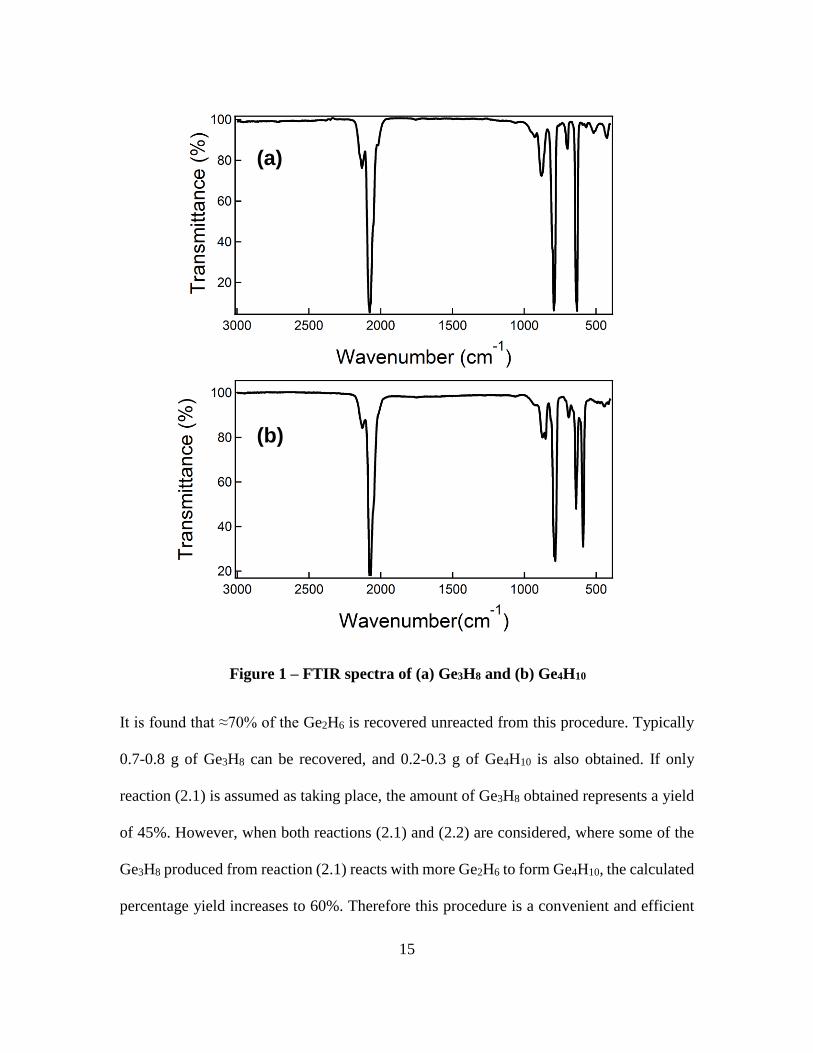
(FTIR). For Ge3H8, the spectrum has peaks at (cm-1) 2131 (m), 2077 (st), 2021 (sh), 928
(w), 879 (m), 794 (st), 700 (w), 632 (st), 594 (vw), 571 (vw), 517 (w), and 424 (w). The
Ge4H10 spectrum contains the peaks (cm-1) 2129 (m), 2075 (vst), 2013 (sh), 874 (m), 852
(m), 793 (st), 785 (st), 692 (w), 640 (st), 592 (st), 445 (w). These spectra are illustrated in
Figure 1 (a) and (b), respectively.
15
It is found that ≈70% of the Ge2H6 is recovered unreacted from this procedure. Typically
0.7-0.8 g of Ge3H8 can be recovered, and 0.2-0.3 g of Ge4H10 is also obtained. If only
reaction (2.1) is assumed as taking place, the amount of Ge3H8 obtained represents a yield
of 45%. However, when both reactions (2.1) and (2.2) are considered, where some of the
Ge3H8 produced from reaction (2.1) reacts with more Ge2H6 to form Ge4H10, the calculated
percentage yield increases to 60%. Therefore this procedure is a convenient and efficient
Figure 1 – FTIR spectra of (a) Ge3H8 and (b) Ge4H10
(a)
(b)

16
method of obtaining higher order germanes. The ratio of Ge3H8 and Ge4H10 products can
also be adjusted if necessary. Reducing the flow rate of the carrier H2 will increase the
amount of Ge4H10 produced. The same effect can be obtained by increasing the density of
the Pyrex wool packing in the reaction zone.
The products were stored at room temperature under H2 atmosphere. No decomposition
was observed over a period of several months. The Ge3H8 product was used in the growth
of doped Ge films described in Chapter 4, as well as in synthesis of GeSn described in
Chapters 5, 6 and 7. The Ge4H10 was used in the fabrication of virtual Ge substrates used
in the same chapters.
3. Synthesis of Deuterostannane
Deuterostannane was synthesized using a modified version of the method reported by
Norman et al.,92 which has been employed in several earlier studies on GeSn.50,93,94 The
synthesis is achieved by reduction of tin(IV) chloride (SnCl4) with lithium aluminium
deuteride (LiAlD4). The SnCl4 was purchased from Sigma-Aldrich. The LiAlD4 was
typically purchased from Cambridge Isotopes, but when it was not available, was easily
synthesized by reducing aluminium chloride (AlCl3) with lithium deuteride (LiD) using the
method described by Finholt and coworkers.95 To conduct the LiAlD4 synthesis, 4.5 g (500
mmol) of finely ground LiD is placed in a 250 mL round bottom flask along with 100 mL
of diethyl ether. This is cooled to -78°C, and 12 g (90 mmol) of anhydrous AlCl3 is
dissolved in ≈60 mL of diethyl ether is slowly added to it via a liquid addition funnel while
stirring under inert atmosphere. The initial stages of addition must be conducted especially
slowly in order to prevent buildup of unreacted AlCl3 in the mixture, which can prompt a

17
vigorous reaction at the start. Once all the AlCl3 is added, the reaction is stirred overnight
while allowing it to warm to room temperature. The liquid, containing dissolved LiAlD4,
is then cannular filtered to a separate vial from which the ether is removed under vacuum.
Typical yield of the solid product obtained in this manner is ≈50%, which may be improved
by successive washing of the residue remaining after the reaction to collect all of the
soluble product.
The SnD4 reaction was carried out in a 3-neck round bottom flask in which 2.5-3.0 g of
LiAlD4 (60-70 mmol) was placed along with 100 mL of dried diglyme, which acts as the
solvent. The SnCl4 (4-5 g, 15-19 mmol) was dissolved in a separate aliquot of diglyme (40
mL), and this solution is slowly added to the LiAlD4 using a jacketed liquid addition funnel.
The jacket was kept at -65°C and the solution in the round bottom flask was kept at -78°C
throughout the addition. The gas generated from the reaction was continuously pumped out
through two traps held at -196°C, while maintaining a slight pressure of ~20 Torr in the
system. The reaction leading to the generation of SnD4 is given below.
SnCl4 + LiAlD4 SnD4 + LiCl + AlCl3 (2.3)
The collected SnD4 may contain trace organic impurities, which can be easily removed by
trap to trap distillation through a pair of -110°C traps, and a -196°C trap is used to collect
the SnD4. This procedure gave SnD4 in yields up to 75%. The purity is verified using FTIR,
and a sample spectrum is given in Figure 2. [FTIR (cm-1): 2704 (vw), 1905 (vw), 1402 (m),
1367 (vst), 1334 (m), 540 (w), 501 (st), 486 (st)].

18
For long term storage of the product, liquid nitrogen temperatures must be used in order to
prevent decomposition. The SnD4 was used in the synthesis of GeSn alloys described in
Chapters 5, 6, and 7.
4. Synthesis of Trisilylphosphine (P(SiH3)3), Trisilylarsine (As(SiH3)3) and
Trisilylstibine (Sb(SiH3)3)
A convenient method for synthesis of trisilyl- group V compounds was reported by
Grzybowki.96 This involves the reaction of the lithium salt Li3M (M=P, As, Sb) with
bromosilane (BrSiH3) or chlorosilane (ClSiH3) in diethylether (Et2O). It was found that
while the use of solvent is more efficient, acceptable yields could be obtained by
performing the reaction in neat ClSiH3. The ClSiH3 was purchased from Voltaix. The Li
salts were synthesized in-house via the reaction of stoichiometric amounts of the respective
elements at 450°C. The general reaction is given below:
Figure 2 – FTIR spectrum of SnD4.

19
Li3M + 3 ClSiH3 M(SiH3)3 + 3 LiCl (M=P, As, Sb) (2.4)
The reaction vessel is a stainless steel cylinder with a volume of ≈20 cm3. The Li salt was
added to the cylinder under inert atmosphere. Typical amounts of salt used were 0.5 g for
Li3P (10 mmol), and 1.0 g for Li3As and Li3Sb (10 mmol and 7 mmol respectively). The
amount of ClSiH3 used was 2.0 g (≈600 LTorr, 32 mmol) for the P and As compounds, and
1.5 g (≈450 LTorr, 24 mmol) for the Sb. This corresponds to a 10-15% excess of ClSiH3,
which was condensed on to the Li salt, and the reaction mixture was allowed to warm up
to room temperature after sealing the vessel. At room temperature, the ClSiH3 is expected
to be in liquid form with a vapor pressure of 6.5 atm.
The reaction was allowed to proceed for 16 hrs for the P compound, and 5 days for the As
and Sb compounds. The trisilylphosphine (P(SiH3)3) was purified by trap-to-trap
distillation through -78°C and -196°C traps, and the -78°C trap contained the pure product,
and the -196°C trap unreacted ClSiH3. The yield of the reaction was 46%. The trisilylarsine
(As(SiH3)3) compound was initially trapped in a -45°C trap, and further purified by a
second distillation through -35°C traps, which removed more volatile impurities. The yield
obtained was 14%. For trisilylstibine (Sb(SiH3)3), a -35°C trap was used to trap out the
pure product. The yield was 2%. The purities of the products were determined through gas
phase FTIR. The observed peaks for the three compounds are given in below in Table 1.
All above compounds were stored at room temperature under inert atmosphere, and were
used in the doping of Ge films and GeSn alloys as described in Chapters 4, 6 and 7.

20
5. Synthesis of Trigermylphosphine
Trigermylphosphine (P(GeH3)3) was synthesized through the reaction of chlorogermane
(ClGeH3) with lithium phosphide (Li3P), as described by Grzybowski.96
Li3P + 3 ClGeH3 P(GeH3)3 + 3 LiCl (2.5)
The Li3P (1 g, 19 mmol) was placed in a 100 mL Schlenk flask under inert atmosphere.
Thereafter, 1300 LTorr of ClGeH3 (70 mmol) was condensed into the reaction vessel,
together with approximately 50 mL of Et2O, which acts as the solvent. The reaction was
stirred overnight at -78°C. The product was separated from unreacted ClGeH3 and the
solvent by trap to trap distillation through -65°C and -196°C traps. The P(GeH3)3 is
collected in the highest temperature trap, together with more volatile impurities believed
to be partially substituted phosphines. These volatile species can be removed by a further
distillation step using -25°C, -60°C, and -196°C traps. The purity of the final product is
confirmed by FTIR [FTIR (cm-1): 2134 (w), 2085 (st), 2001 (w), 957 (w), 882 (m), 838
(m), 802 (vst), 564 (w), 515 (w)].
Table 1 – FTIR absorption frequencies of P(SiH3)3, As(SiH3)3 and Sb(SiH3)3
FTIR(cm-1)
P(SiH3)3 As(SiH3)3 Sb(SiH3)3
2171(st) 2165(st) 2162(st)
1866(vw) 1125(w) 1869(w)
1124(m) 933(st) 1119(w)
947(st) 873(st) 956(m)
937(st) 769(vw) 901(m)
746(w) 595(w) 851(st)
625(w) 542(w) 762(w)
572(w) 570(w)
467(w)

21
The final yield obtained is 27%, similar to the 20% reported by Grzybowski.96 P(GeH3)3
can be stored in a dry-box freezer kept at -25°C for several months with minimal
decomposition. It was used for doping GeSn alloys as described in Chapter 6, and in the
fabrication of n-type doped virtual Ge substrates, as described in Chapter 7.
6. Synthesis of Deuterostibine
Deuterostibine (SbD3) was synthesized by reducing antimony(III) chloride (SbCl3) with
LiAlD4, a method which was first described by Todd et al.97 (who also used sodium
borodeuteride as the reducing agent) based on the following reaction:
4 SbCl3 + 3 LiAlD4 4 SbD3 + 3 LiCl + 3 AlCl3 (2.6)
The reaction was conducted in a two-neck round bottom flask in which 0.3 g of LiAlD4
(7 mmol) dissolved in 40 mL of diglyme was placed. This solution was cooled to -70°C,
and a solution containing 0.5 g SbCl3 (2 mmol) in diglyme held at -50°C was slowly added
to it via an addition funnel. The system was dynamically pumped such that the pressure
was kept at 20 Torr, and the removed gases were pulled through traps held at -78°C and
-196°C. The first trap condenses most volatile organic impurities, while the product
condenses in the -196°C traps. Once the addition was complete, the reaction mixture was
allowed to warm up to room temperature to allow the reaction to reach completion.
Continuous removal of the generated gases was maintained during the warm up process.
The product collected in the -196°C traps contains minor quantities of organic impurities,
which can be removed by sequential trap to trap distillations through -110°C and -196°C
traps, where the former collects the impurities. The final yield of pure product is 60%, and
the FTIR spectrum [FTIR (cm-1): 2686 (vw), 1892 (vw), 1628 (vw), 1400 (m), 1360 (st),

22
1321 (m), 1223 (vw), 592 (m), 559 (m)] was compared with accepted literature values to
validate the purity.97 The product can be stored at room temperature for several weeks
when the pressure of the gas is kept below 10 Torr. SbD3 was used for the doping of Ge
films and GeSn alloys, as described in Chapters 4 and 6 respectively.
7. Synthesis of Disilylsulfide
Literature methods for the synthesis of disilylsulfide (S(SiH3)2) involves either toxic Hg
compounds, or organic solvents.98 Due to the difficulties posed when using these methods,
an alternative synthetic route was developed to obtain viable quantities of semiconductor
grade S(SiH3)2. This involves the reaction of bis(triphenyltin)sulfide (S(SnPh3)2) with
bromosilane (BrSiH3), as described by the equation below. The S(SnPh3)2 is commercially
available from Gelest and was used as received, while the BrSiH3 was synthesized in house
by reacting phenylsilane (PhSiH3) with hydrogen bromide (HBr).
S(SnPh3)2 + 2 BrSiH3 S(SiH3)2 + 2 BrSnPh3 (2.7)
The above reaction was conducted by placing 3.6 g of S(SnPh3)2 (5 mmol) in a Schlenk
flask under inert atmosphere and then condensing 90% excess of BrSiH3 (350 LTorr, 19
mmol) onto this solid. The mixture was then allowed to warm up to -10°C, at which
temperature the reaction was allowed to proceed for 1 hr. Trap to trap distillation was then
used to purify the product. A -78°C trap was found to condense the S(SiH3)2, while
unreacted BrSiH3 was recovered using -196°C traps. The yield of the reaction is 60%.
FTIR and NMR were used to identify the product and to ensure its purity [FTIR (cm-1):
2186 (st), 956 (st), 916 (vst), 907 (st), 640 (w), 529 (m), 510 (m)]. The NMR spectrum of
the product collected using CDCl3 solvent shows a strong singlet at 4.389 ppm and satellite

23
peaks at 4.108/4.672 ppm associated with the equivalent –SiH3 protons and the splitting
of this signal by the 29Si isotope, as shown in Figure 3. This compound was used for doping
Ge with S as described in Chapter 4.
4.5 4.0
Chemical Shift (ppm)
4.1
1
4.3
9
4.6
7
Figure 3 - 1H NMR spectrum of S(SiH3)2 in CDCl3 solvent
8. Synthesis of Digermylsulfide
For the synthesis of digermylsulfide (S(GeH3)2), a metathesis reaction was first reported
by Goldfarb and Sujishi which used S(SiH3)2 and chlorogermane (ClGeH3) as the starting
materials.99 The synthetic procedure for S(SiH3)2 was described above, while the ClGH3
can be easily synthesized by chlorinating GeH4 with SnCl4.100 The reaction was conducted
in a thick walled Pyrex container equipped with a vacuum valve. Both reactants were
condensed into the vessel and it was then allowed to warm up to room temperature. The
reaction is instantaneous and is given below.

24
S(SiH3)2 + 2 ClGeH3 S(GeH3)2 + 2 ClSiH3 (2.8)
After 5 min at room temperature, the product was purified using trap-to-trap distillation,
and a trap held at -60°C was found to condense the product, which was further purified by
passing through a pair of -30°C traps to remove volatile impurities. Starting from 35 LTorr
(1.9 mmol) of S(SiH3)2 and 75 LTorr (4.0 mmol) of ClGeH3, it was possible to obtain 15
LTorr (0.8 mmol) of the product, which is a yield of 45%. The purity of the product was
verified by comparing the FTIR spectra (cm-1) at 2104 (st), 2084 (st), 847 (m), 855 (m),
825 (vst), 578 (w), 555 (w), 412 (m) to literature values.99 The NMR spectrum shows a
singlet at 4.716 ppm associated with the –GeH3 protons, as shown below in Figure 4.
The S(GeH3)2 is unstable at room temperature, but could be stored at -25°C in a dry-box
freezer for extended periods. It was used for doping of Ge as described in Chapter 4.
9. Synthesis of Diborane
Diborane (B2H6) was synthesized using methods described by Norman et al.101 In order to
conduct the reaction, 35 mL of syrupy phosphoric acid (H3PO4) was added to a 500 mL
round bottom flask and degassed by applying vacuum for several hours. The other reactant,
potassium borohydride (KBH4) was ground to a fine powder inside a dry-box, and placed
in a side arm solid addition tube. The amount used was 1.7 g (32 mmol). The tube was
connected to the flask using Schlenk techniques and the setup was evacuated. The solid
was then slowly added to the acid over a period of ~1 hr with continuous stirring. The
reaction generates B2H6 according to the following reaction.
2 H3PO4 + 2 KBH4 B2H6 + 2 KH2PO4 + 2 H2 (2.9)

25
4.80 4.75 4.70 4.65
Chemical Shift (ppm)
4.7
2
Figure 4 - 1H NMR spectrum of S(GeH3)2 in CDCl3 solvent
The generated gases are pumped through -78°C and -196°C traps. The former collects
water vapor, and the product is trapped in the latter. The H2 byproduct is pumped away.
B2H6, which is a colorless gas at room temperature was obtained in a 35% yield. The FTIR
spectrum exhibits peaks (cm-1) 3660 (w), 2627 (m), 2594 (m), 2540 (m), 2519 (st), 2499
(m), 2345 (w), 1867 (w), 1622 (st), 1600 (vst), 1583 (st), 1194 (m), 1174 (m), 1153 (m),
974 (w), which agree well with literature values for B2H6.99

26
CHAPTER THREE
High-Order Ge-Hydride Chemistry for Low Temperature Ge Based Materials
Fabrication: A Study of Pentagermane
Synopsis
This chapter presents a study of the synthesis of the high order Ge hydride pentagermane
(Ge5H12) via thermolysis reactions previously used for the synthesis of Ge3H8 and Ge4H10.
The thermodynamic properties of the various isomers and reaction pathways leading to the
desired product are explored by computational methods, and the results are compared to
experimental observations. Finally, Ge5H12 is used in proof-of-principle experiments
which demonstrate its viability as a precursor for epitaxy of high quality Ge on Si at low
temperatures of ≈350°C.
Portions of this chapter were previously published by Grzybowski, G.; Chizmeshya, A. V.
G.; Senaratne, C.; Menendez, J.; Kouvetakis, J. Fundamental experimental and theoretical
aspects of high-order Ge-hydride chemistry for versatile low-temperature Ge-based
materials fabrication. J. Mater. Chem. C 2013, 1 (34), 5223. Reproduced by permission of
The Royal Society of Chemistry.
1. Introduction
As mentioned in Chapter 1, Ge based materials are being extensively researched for use in
fabricating components for optoelectronic and microelectronic devices integrated on to Si.
Recent progress in growth of Ge directly of Si(100) has led to the development of novel
devices such as Ge based lasers10,11 and IR photodetectors.8 Several techniques have been
utilized for the production of atomically flat, defect free Ge on Si epilayers for such

27
applications, such as the use of Si1-xGex graded buffer layers102 or growth of an initiation
layer at low temperatures (~320°C) followed by higher temperature (600°C) growth of the
bulk material.103–105 The former technique requires a graded buffer of several microns and
is therefore difficult to implement in low cost applications. The major drawback of the
latter technique is the incompatibility with CMOS processing conditions, due to the
requirement of high growth temperature.
In this context, the high order Ge hydrides Ge3H8 and Ge4H10 were first developed at ASU
as an ideal way to simultaneously achieve the dual requirements of high crystalline quality
and low growth temperatures.91 The synthetic procedures for producing these precursors
were described in Chapter 2. In addition to growth of Ge on Si, these compounds were later
used for synthesis of GeSn binary and germanium-silicon-tin (GeSiSn) ternary alloys,106,107
an aspect that will be further explored in later chapters. Among these compounds, Ge4H10
was recently employed by Xu et al. to develop optimized synthetic procedures for
producing Ge on Si films with device quality properties for subsequent applications as
compliant platforms on Si.77 The Ge films produced in the above work have thicknesses in
the order of several microns and surface roughness < 1 nm indicating layer by layer growth.
A maximum growth rate of 30 nm/min was observed at 400°C. Their deposition protocols
have atomic incorporation efficiencies up to 50%, and are therefore suitable for low cost,
high-throughput industrial processes. Ge on Si pin photodetectors were also fabricated
using this technique, validating its practical utility. This procedure for producing high
quality Ge films on Si will be extensively used in work described in subsequent chapters.

28
The successful introduction of Ge4H10 as a viable deposition technology suggests that
pentagermane (Ge5H12) and its various branched isomers are in principle the next logical
choice in the oligomeric series of potential germyl hydride precursors for next generation,
low temperature semiconductor processing. From a chemical point of view Ge5H12 may
in fact possess comparable reactivity to that of Ge4H10, but its significantly larger mass
(375 amu) implies that the compound condenses as a high boiling point liquid with
diminished vapor pressure at ambient conditions. The expected lack of volatility in this
case represents a significant barrier towards adoption in vapor deposition techniques,
suggesting that any further materials gains will be difficult to realize using standard
vacuum based approaches. Alternatively, this compound may represent a useful delivery
source in liquid form for atomic layer deposition (ALD) of devices requiring selective
growth of nanoscale transistor architectures, since it may be potentially evaporated in situ
as needed. On the other hand, the liquid compound may be suitable for solution-based
depositions of semiconductor layers with bulk-like properties, since it exhibits a reasonable
stability at room temperature and a facile thermal reactivity. The latter growth technique
has attracted increasing attention recently in the ubiquitous silicon technology arena where
thermal processing of liquid phase hydrides has been successfully implemented to
manufacture electronic devices, opening the door for large-scale high-volume production
via spin coating approaches. For example Si films have been grown via photochemical
transformations or heat treatments of solutions containing either cyclopentasilane
(Si5H10)108 or cyclohexasilane (Si6H12).
109 In this regard silicon films have also been
produced via thermal decomposition of Si5(C6H5)10.110 As in the case of Ge5H12, these
compounds are of very limited utility as conventional CVD sources due to negligible vapor
29
pressures. However, the enhanced reactivity of Si5H10 allows complete and controllable
elimination of the hydrogen atoms from the molecular cores to produce semiconductor
structures and working thin-film transistors exhibiting state-of-the-art characteristics. In
this context, analogous Ge-based technologies may be accessible using solvent-processable
Ge5H10 sources whose intrinsic properties seem to be ideal for this solution-type thin film
crystal growth.
In view of the potential applications of Ge5H12, we explored synthetic pathways from both
experimental and theoretical perspectives to produce this compound in high yield. As
discussed in Chapter 2, high-order species can be obtained using a strategy based on
reactions (3.1) and (3.2). The same strategy can be extended to obtain Ge5H12 as described
by reaction (3.3).
Ge2H6 + Ge2H6 GeH4 Ge3H8 Rx
Ge2H6 + Ge3H8 GeH4 + Ge4H10 Rx(3.2)
Ge2H6 + Ge4H10 GeH4 + Ge5H12 Rx(3.3)
To our knowledge, the synthetic scheme proposed above has never been reported. To study
this possibility we conducted stoichiometric thermolysis reactions of gaseous Ge2H6 and
Ge3H8 at 250°C , and we obtained Ge4H10 (about 25-30 %) and small amounts of Ge5H10,
suggesting the validity of eq. 3.2 and 3.3. To explain this outcome we propose a reaction
mechanism by which the Ge2H6 starting material initially dissociates to form reactive GeH2
intermediates. These in turn insert into existing Ge-Ge bonds of the co-reactant molecule
to form the higher-order analog. To elucidate the thermodynamics underpinning the

30
observed tendency for the formation of Ge3H8 in (3.1), and its subsequent use to produce
Ge4H10 in (3.2), we calculated the free energies for (3.1)-(3.3) for a range of temperatures
relevant to our experimental studies. The data indicate that the driving force for all above
reactions is favorable, in agreement with the trends observed experimentally. In addition,
as a part of our comprehensive study of germanium heavy hydrides we also carried out
DFT-based simulations to obtain some fundamental properties of Ge5H12, as previously
done for the Ge4H10 analog.107
2. Thermochemistry Simulations
A distinctive aspect of Ge5H12 is that it can adopt neo-, iso- and n-like isomeric forms
corresponding to centered, branched or chained structures, with additional conformal
variants within the branched and chained families. Here in our calculations we consider
seven distinct isomers: neo-Ge5H12, two branched conformers (i1-Ge5H12 and i2-Ge5H12)
and four chained isomers derived from the linear chain n-Ge5H12 but exhibiting various
anti-gauche combinations. Accordingly, one objective of our computational work is to
generate simulated IR spectra for all possible pentagermane isomers, for use in comparative
“fingerprinting” with the observed spectra of gas phase precursor molecules, which are
presumed to exist as an isomer mixture. Perhaps more importantly the purpose of our
simulation studies is to: (i) identify the most thermodynamically stable pentagermane
isomer species, and (ii) study reaction pathways to the desired Ge4H10 and Ge5H12 species
as the main product in order to maximize their yield, as indicated above. In this connection,
our related studies on tetragermane predicted that the free-energy of the i-Ge4H10 species
is ~4.4 kJ/mol lower than that of either the n-Ge4H10 and g-Ge4H10 isomers at standard
conditions.107 As demonstrated below the corresponding free-energy ordering in

31
pentagermane exhibits a very similar trend, with the i-Ge5H12 being lower in free-energy
than the neo-Ge5H12 or n-Ge5H12 isomers. These results are expected to provide valuable
guidance in the design of experiments to produce Ge4H10 and Ge5H12, which may be
considered to be the ultimate high-efficiency Ge sources for the next generation device
applications.
The computational approach adopted here follows that used in our prior successful studies
on a wide range of lighter Ge-based hydrides, and is based on the use of B3LYP hybrid
density functional theory (DFT) in conjunction with a standard 6-311G++(3df,3pd) basis
set, as implemented in the Gaussian03 code.111 All calculations were performed using
automatically generated auxiliary basis sets for charge density fitting and default
convergence criteria for the self consistent field convergence and structure optimizations.
Special care was taken to avoid grid pruning effects such as the generation of “noisy”
structures leading to spurious soft-modes (typically associated with –GeH3 rotor motion).
Accordingly we consistently used the so-called “UltraFine” integration grid option in all
calculations and verified that the harmonic normal mode frequencies are positive definite
in all cases, indicating that the corresponding ground state structures are dynamically
stable. The molecular structures and corresponding thermodynamic data for all isomers are
summarized in Tables 2 and 3.
The standard thermochemistry output from Gaussian03 at T=298K and P=1 atm is
summarized in Table 3 and includes the static electronic energy of the molecules, E0, as
well as their thermally corrected counterparts for the free-energy (E0+Gth). Based on a
harmonic treatment for thermodynamic corrections the branched i1-Ge5H12 is predicted to

32
Ta
ble
2 -
Su
mm
ary
of
stru
ctu
ral
an
d e
nerg
etic
res
ult
s fo
r is
om
ers
of
pen
tager
ma
ne.
Th
e
an
d
des
ign
ati
on
s re
fer
to
exte
rnal
an
d i
nte
rnal
Ge-
Ge
bon
d l
ength
s, r
esp
ecti
vel
y.
Ge-G
e-G
e b
on
d a
ngle
s co
nta
inin
g a
3 o
r 4 c
ente
red
Ge
are
den
ote
d u
sin
g
, w
hil
e th
ose
in
volv
ing a
seq
uen
ce o
f ch
ain
ed a
tom
s are
lab
eled
wit
h
. T
he
sub
scri
pts
“T
” a
nd
“S
” r
efer
(res
pec
tivel
y)
to t
erm
inal
an
d s
agit
tal
Ge-
H b
on
d l
ength
or
H-G
e-H
bon
d a
ngle
sp
ecie
s, w
hil
e an
ast
eri
sk d
enote
s a –
Ge-
H m
oie
ty b
on
d l
ength
.
Des
ign
ati
on
n
eo-
Ge 5
H1
2
i 1-G
e 5H
12
i 2-G
e 5H
12
n1-G
e 5H
12
n2-G
e 5H
12
n3-G
e 5H
12
n4-G
e 5H
12
Po
int
Gro
up
T
d
C1
Cs
C2
v
C1
C2
Cs
Bo
nd
Len
gth
s (Å
)
(
Ge-G
e)
2.4
45 (
4)
2.4
51(x
2),
2.4
46
2
.45
0(
2),
2.4
45
2
.44
6(
2)
2.4
45(
2)
2.4
44(
2)
2.4
44(
2),
2.4
51
(
Ge-
Ge)
--
2
.45
5
2.4
57
2.4
50(
2)
2.4
50(
2)
2.4
51(
2)
2.4
51(
2)
(Ge-
H) T
1
.53
8
(1
2)
1.5
38(
9)
1.5
38(
9)
1.5
38(
6)
1.5
38(
6)
1.5
37(×
6)
1.5
37(×
2),
1.5
38
(Ge-
H) S
--
1
.54
2(
2),
1.5
46
*
1.5
42(
2),
1.5
47
*
1.5
42(
6)
1.5
42(
6)
1.5
42(×
6)
1.5
42
Bo
nd
an
gle
s
(deg
rees
)
Ge-
Ge-G
e
10
9.5
1
11
.2,
111
.6,
11
1.0
1
11
.6,
111
.7(
2)
--
--
--
--
Ge-
Ge-
Ge
--
11
3.5
1
13
.8
11
3.4
(2),
11
2.8
11
3.1
(2),
11
3.3
11
3.1
(2),
11
3.5
11
4.1
(2),
11
3.6
(H-G
e-H
) T
10
8.5
(1
2)
10
8.4
-108
.5
10
8.3
-108
.5
10
8.4
-108
.5
10
8.4
-108
.5
10
8.4
-108
.5
10
8.4
,
10
8.5
(2)
(H-G
e-H
) S
--
10
7.1
1
07
.2
10
7.1
(2),
10
6.9
10
7.3
(2),
10
7.1
10
7.2
(2),
10
7.1
10
7.3
Dip
ole
Mo
men
t (D
) 0
.00
00
0.0
623
0.0
451
0.0
225
0
.02
37
0.0
031
0
.03
61

33
Tab
le 3
- T
her
mo
chem
istr
y d
ata
for
the
isom
ers
dep
icte
d i
n T
ab
le 2
, w
hic
h i
ncl
ud
es t
he
elec
tron
ic g
rou
nd
sta
te e
ner
gy
E0, an
d t
he
free
-en
erg
y c
on
trib
uti
on
Gth
. M
od
e in
dic
es f
or
roto
rs a
re
list
ed t
oget
her
wit
h t
hei
r h
arm
on
ic f
req
uen
cies
an
d
thei
r co
rres
pon
din
g p
art
itio
n f
un
ctio
n c
on
trib
uti
on
s to
th
e fr
ee e
ner
gy.
Th
e n
et c
orr
ect
ion
to t
he
free-e
nerg
y f
or
the
hin
der
ed r
oto
r ap
pro
xim
ati
on
are
lis
ted
as
Gth
HR.
Des
ign
ati
on
n
eo-G
e 5H
12
i 1-G
e5H
12
i 2-G
e 5H
12
n1-G
e 5H
12
n2-G
e 5H
12
n3-G
e 5H
12
n4-G
e 5H
12
Th
erm
och
em
istr
y
(T=
29
8K
, P
=1
atm
)
E0 (
H)
-10
39
2.3
25
01
-1
03
92
.32
357
-1
03
92
.32
306
-1
03
92
.32
333
-1
03
92
.32
279
-1
03
92
.32
228
-1
03
92
.32
193
E
0 (
kJ/
mo
l)
0
+3
.8
+5
.1
+4
.4
+5
.8
+7
.2
+8
.1
Ha
rm
on
ic (
T=
29
8K
, 1
atm
)
Gth
(H
) 0
.04
86
7
0.0
460
6
0.0
477
2
0.0
472
2
0.0
478
3
0.0
473
0
0.0
481
2
E0+
Gth
(H
) -1
03
92
.27
634
-1
03
92
.27
751
-1
03
92
.27
534
-1
03
92
.27
611
-1
03
92
.27
496
-1
03
92
.27
498
-1
03
92
.27
381
(E
0 +
Gth
) (k
J/m
ol)
+
3.1
0
+
5.7
+
3.7
+
6.7
+
6.6
+
9.7
Hin
d.
Ro
tors
Co
rrec
ted
(T=
29
8K
, 1
atm
)
G
th H
R(H
) +
0.0
001
39
+
0.0
000
14
-0
.00
07
90
-0
.00
03
18
-0
.00
05
95
-0
.00
00
37
-0
.00
07
08
E0+
Gth
(H
) -1
03
92
.27
620
-1
03
92
.27
750
-1
03
92
.27
613
-1
03
92
.27
643
-1
03
92
.27
556
-1
03
92
.27
502
-1
03
92
.27
452
(E
0 +
Gth
) (k
J/m
ol)
+
3.4
0
+
3.6
+
2.8
+
5.1
+
6.5
+
7.8
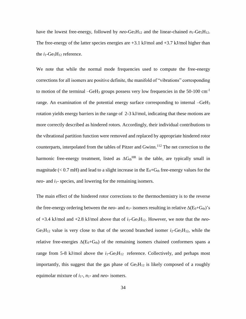
34
have the lowest free-energy, followed by neo-Ge5H12 and the linear-chained n1-Ge5H12.
The free-energy of the latter species energies are +3.1 kJ/mol and +3.7 kJ/mol higher than
the i1-Ge5H12 reference.
We note that while the normal mode frequencies used to compute the free-energy
corrections for all isomers are positive definite, the manifold of “vibrations” corresponding
to motion of the terminal –GeH3 groups possess very low frequencies in the 50-100 cm-1
range. An examination of the potential energy surface corresponding to internal –GeH3
rotation yields energy barriers in the range of 2-3 kJ/mol, indicating that these motions are
more correctly described as hindered rotors. Accordingly, their individual contributions to
the vibrational partition function were removed and replaced by appropriate hindered rotor
counterparts, interpolated from the tables of Pitzer and Gwinn.112 The net correction to the
harmonic free-energy treatment, listed as GthHR in the table, are typically small in
magnitude (< 0.7 mH) and lead to a slight increase in the E0+Gth free-energy values for the
neo- and i1- species, and lowering for the remaining isomers.
The main effect of the hindered rotor corrections to the thermochemistry is to the reverse
the free-energy ordering between the neo- and n1- isomers resulting in relative (E0+Gth)’s
of +3.4 kJ/mol and +2.8 kJ/mol above that of i1-Ge5H12. However, we note that the neo-
Ge5H12 value is very close to that of the second branched isomer i2-Ge5H12, while the
relative free-energies (E0+Gth) of the remaining isomers chained conformers spans a
range from 5-8 kJ/mol above the i1-Ge5H12 reference. Collectively, and perhaps most
importantly, this suggest that the gas phase of Ge5H12 is likely composed of a roughly
equimolar mixture of i1-, n1- and neo- isomers.

35
3. Simulation of Vibrational Properties
Our main objective here is to systematically compare the vibrational spectra of
pentagermane isomers in order to identify any features that could be used to distinguish or
identify Ge5H12 from its lighter Ge-hydride relatives, and tetragermane in particular which
is expected to possess very similar properties. Typically these two compounds are
separated by distillation and the gas phase IR spectra could in principle be used to establish
their purity provided that distinguishing features exist. Figure 5 contains the main results
of our calculations, separated into two categories corresponding to high-frequency Ge-H
stretching vibrations (2000-2200 cm-1), and lower frequency Ge-H wagging and bending
motions as well as Ge-backbone vibrations (<1000 cm-1). The frequencies in these plots
were not scaled. However, well-established scale factors 0.995 and 0.975 for the low and
high frequency ranges, respectively, are supported by much of our prior work on Si and Ge
based hydrides at this level of theory and were used in our comparisons with observed
spectra, below.
Here we describe the general trends by frequency range and intensity. For example, the
very weak features occurring below about 400 cm-1 can be classified as follows: (i) The
lowest frequency modes (< 100 cm-1) are due to rotational motion of the terminal GeH3
groups, (ii) torsional Ge-backbone vibrations occur between ~100-200 cm-1, (iii) rocking
–GeH2- and -GeH3 vibrations perpendicular to the -Ge-Ge- bonds are found in the 200-300
cm-1 range. More intense spectral features are found in the 400-700 cm-1 range and are
assigned to in-phase –GeH2- wagging motions parallel to the –Ge-Ge- backbone bonds
(500-600 cm-1), and their out-of-phase counterparts (600-700 cm-1). A series of typically
well-separated bands associated with in-phase proton wagging in the –GeH3 groups occur
36
in the 700-850 cm-1 range. Finally, vibrations with frequencies 850-900 cm-1 are assigned
to “scissor” motion of the protons in the –GeH2- and –GeH3 groups, perpendicular to the -
Ge-Ge- bonds. The most intense band among all of the isomers is found in neo-Ge5H12
near ~780 cm-1, and is due to concerted proton wagging directed along the axial Ge-Ge
bond directions. The higher frequency portions of the calculated isomer spectra are also
shown in the left panel of Figure 5, and indicate the usual complex band of frequencies
corresponding to symmetric and anti-symmetric Ge-H stretches in various in-phase and
anti-phase combinations. In general we find that the principal assignments are virtually
identical to those reported in prior work on tetragermane. Another comparatively strong
feature, found in the spectrum of the n1-Ge5H12 linear-chain conformer, devolves from
highly coherent in-phase –GeH2- wagging motions parallel to the backbone. Due to its
exclusive low-frequency position near ~560 cm-1 in relation to the spectra of all of the
Figure 5 - Summary of simulated infrared spectra for the Ge5H12 isomers in the low-
frequency (left) and high-frequency (right) regimes. Relative free energies of the
isomers are provided on the right and the dashed horizontal lines separate the three
isomer families, identified as neo-, branched and chained.
37
remaining isomers the latter represents a key distinguishing “fingerprint” for the Ge5H12
compound. This is discussed in more detail below, in the context of experimental
characterization.
4. Reaction Thermodynamics of Higher Order Ge-Hydrides
Here we envision that all high order germanes can be formed from the pyrolysis of an initial
mixture of lower order germanes such as digermane and trigermane via insertion reactions
involving a reactive germylene intermediate GeH2. The germylene is presumed to
successively react with higher order polygermanes according to a cascade sequence,
culminating in the formation of pentagermane according to the following reactions:
Ge2H6 GeH2 + GeH4 G0R,1 = +119.6 kJ/mol Rx(3.4)
GeH2 + Ge2H6 Ge3H8 G0R,2 = –128.9 kJ/mol Rx(3.5)
GeH2 + Ge3H8 i-Ge4 H10 G0R,3 = –127.2 kJ/mol Rx(3.6)
GeH2 + i-Ge4 H10 i-Ge5 H12 G0R,4 = –127.3 kJ/mol Rx(3.7)
The reaction free energies listed here were all obtained using thermochemistry calculations
as described earlier, namely at the B3LYP/6-311++(3pd,3df) level. Our simple model does
not include isomeric branching in the tetra- and pentagermane reactions. Instead, for the
purpose of our preliminary studies here we use the most thermodynamically favorable
higher-order isomer species at 298K (i-Ge4H10 and i1-Ge5H12). The thermochemistry and
structural trends for GeH4, Ge2H6, Ge3H8, and i-Ge4H10 closely follow those reported in
our prior work,107 while the values for i-Ge5H12 were taken from Table 3 above. The 298K

38
equilibrium constants corresponding to the G values listed in Rx(3.4)-Rx(3.7) are found
to be 210
4, 101052.1 PK , 220
5, 108886.3 PK , 220
6, 109884.1 PK and
220
7, 100288.2 PK . Introducing extent of reaction variables {x,y,u,v} for the above
processes, and assuming that the reactions are initiated using 0
Dn moles of digermane, the
mass balance the simultaneous equilibrium condition in the ideal gas approximation are
represented by the set of coupled equations:
Myxn
xK
D
P)( 0
0
4,
;Myxn
uyK
D
P
1
)(
)(0
0
5,
;
Muy
vuKP
1
)(
)(0
6,
;
Mvu
vKP
1
)(
0
7,
(3.8)
where we have defined the function . Solution of
these simultaneous equilibrium equations at T= 300 K and P = 1 atm, yields a mixture of
~68% GeH4, ~4% Ge2H6, ~8% Ge3H8, ~10% Ge4H10 and ~12% Ge5H12 and a vanishing
concentration of the GeH2 germylene intermediate. A simpler alternative approach is to
subsume the germylene insertion reactions by subtracting Rx(3.4) from Rx(3.5), Rx(3.6)
and Rx(3.7), respectively, to obtain a completely equivalent set of effective reactions
equations given earlier in the chapter as Rx(3.1)-Rx(3.3):
Ge2H6 + Ge2H6 GeH4 Ge3H8 G0R,1 = –9.35 kJ/mol
Ge2H6 + Ge3H8 GeH4 i-Ge4H10 G0R,2 = –7.67 kJ/mol
Ge2H6 + i-Ge4H10 GeH4 i-Ge5H12 G0R,3 = –7.76 kJ/mol
M (x, y,u,v;P) =(x - y -u - v)
(nD
0 + x - y -u- v)
P
PO

39
with corresponding equilibrium constants 43.4455 0
1, PK , 22.10470
2, PK and
22.84250
3, PK .
In the ideal gas approximation the pressure dependence of the reactions vanishes due to the
equimolar balance between reactants and products yielding simultaneous equilibrium
equations
20
000
1,)2(
))((
zyxn
zyxnyxnK
D
GTP
Eq(3.9)
)2)((
))((00
00
2,zyxnyxn
zyxnzyK
DT
GP
Eq(3.10)
)2)((
)(0
00
3,zyxnzy
zyxnzK
D
GP
Eq(3.11)
where {x,y,z} now represent the extent of reaction in Rx(3.1), Rx(3.2) and Rx(3.3),
respectively, and nG0, nD
0 and nT0 denote the amount of GeH4, Ge2H6 and Ge3H8 in the
initial reaction mixture. Numerical solution of these equations at T=298K and P=1 atm,
with digermane as the sole reactant yields an equilibrium mixture of ~68% GeH4, ~4%
Ge2H6, ~8% Ge3H8, ~10% Ge4H10 and ~12% Ge5H12, in accord with our earlier results
obtained for the germylene reactions. Collectively the above models predict that germane
is expected to be the dominant equilibrium species, with ~25-30% of the product
represented by higher order germanes for a broad range of initial reactant mixtures. In
future work this model could be further refined by incorporating fugacity corrections to the

40
ideal gas treatment, and more sophisticated statistical mechanics models for the
thermodynamic functions.
Next the free energies were calculated for reactions Rx(3.1)-Rx(3.3) as a function of
temperature up to ~ 430oC (700K) and P = 1 atm, and the results are plotted in Figure 6.
The graphs indicate that all reactions are expected to be spontaneous over this temperature
range with trigermane production via Rx(3.1) representing the main “driving force”. While
the corresponding tetragermane and pentagermane reaction free energies are predicted to
be comparable at ambient conditions our simulations predict that pentagermane reaction is
slightly favored at high temperatures compared to its tetragermane counterpart. The data
used to produce the latter figure was then used to explore the temperature dependence of
the product yields by repeatedly solving the equilibrium equations over the 300-700K
temperature range for various initial reactant mixtures. Figure 7 compares the temperature
dependence of the equilibrium yields for reactions initiated with pure digermane and an
initial equimolar mixture of digermane and trigermane. From the plots it is evident that the
Figure 6 - Temperature dependence of the reaction free energies G0R,1 (black),
G0R,2 (red) and G0
R,3 (blue), in kJ/mol

41
qualitative trends are similar for both initial conditions, and that GeH4 is the dominant
species across the entire temperature range.
The above conclusions are consistent with experimental thermolysis of pure digermane in
a closed vessel yielding GeH4 as the main product and relatively large concentrations of
non-volatile liquid, which is tentatively identified as pentagermane. The vapor pressure of
the corresponding gas phase above this liquid was estimated to be in the range of ~ 0.1-0.2
Torr, which is significantly smaller and distinct from that of tetragermane (~1.5 Torr).
The volatility of this liquid sample was nevertheless sufficient to acquire a reliable and
reproducible gas-phase infrared spectrum, which bore a close resemblance to that of its
tetragermane counterpart, with the exception of a sharp peak in the vicinity of ~ 570 cm-1
consistent with the theoretical predictions described above for pentagermane. This
spectrum, along with its liquid phase counterpart are compared with the corresponding gas
and liquid phase spectra of tetragermane in Figure 8. The gas phase reference IR spectrum
Figure 7 - Temperature dependence of the equilibrium concentrations for the
reaction system described by Rx(3.1)-Rx(3.3) initiated using pure Ge2H6 (left panel)
and an equimolar mixture of Ge2H6 and Ge3H8 (right panel) .
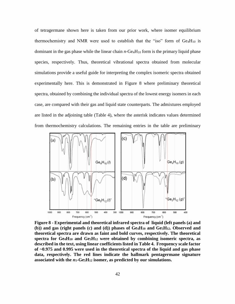
42
of tetragermane shown here is taken from our prior work, where isomer equilibrium
thermochemistry and NMR were used to establish that the “iso” form of Ge4H10 is
dominant in the gas phase while the linear chain n-Ge4H10 form is the primary liquid phase
species, respectively. Thus, theoretical vibrational spectra obtained from molecular
simulations provide a useful guide for interpreting the complex isomeric spectra obtained
experimentally here. This is demonstrated in Figure 8 where preliminary theoretical
spectra, obtained by combining the individual spectra of the lowest energy isomers in each
case, are compared with their gas and liquid state counterparts. The admixtures employed
are listed in the adjoining table (Table 4), where the asterisk indicates values determined
from thermochemistry calculations. The remaining entries in the table are preliminary
Figure 8 - Experimental and theoretical infrared spectra of liquid (left panels (a) and
(b)) and gas (right panels (c) and (d)) phases of Ge4H10 and Ge5H12. Observed and
theoretical spectra are drawn as faint and bold curves, respectively. The theoretical
spectra for Ge4H10 and Ge5H12 were obtained by combining isomeric spectra, as
described in the text, using linear coefficients listed in Table 4. Frequency scale factor
of ~0.975 and 0.995 were used in the theoretical spectra of the liquid and gas phase
data, respectively. The red lines indicate the hallmark pentagermane signature
associated with the n1-Ge5H12 isomer, as predicted by our simulations.

43
estimates based on fitting. Such simulations provide a useful guide for interpreting the
complex isomeric spectra obtained experimentally.
As can be seen from our comparisons, all of the main features of the gas and liquid phase
infrared spectra are reasonably accounted for using our thermochemistry simulations, and
are also qualitatively consistent with observations from earlier studies.113 In the latter,
pentagermanes were generated in very small amounts relative to lower order analogs using
silent discharge of monogermane. Chromatographic separation of the Ge5H12 then yielded
iso- and n- Ge5H12 conformers as dominant components in the mixture, while the neo-
analog fraction was found to be vanishingly small. These trends are in general agreement
with both our fit, and our proposed assignment of the observed peak intensities associated
with three isomers. In the case of our liquid phase comparisons the simulated spectra were
obtained using 50% i1-Ge5H12, 40% n1-Ge5H12 and 10% neo-Ge5H12. In this regard, the
high concentration of the iso- species in our liquid samples is consistent with our high-
Table 4 - Isomer admixtures used to generate the theoretical spectra shown in
Figure 8. The asterisk denotes values determined from thermochemistry
calculations reported in Ref 107. The remaining entries are obtained using a
simple linear combination fit.
Ge4H10
iso linear gauche
gaseous * 80 % 12 % 8 %
liquid 15 % 70 % 15 %
Ge5H12
neo linear (n1) iso (i1)
gaseous 10 % 50 % 40 %
liquid 15 % 70 % 15 %

44
resolution NMR analysis which clearly resolves both conformers. We note that the
corresponding NMR data reported in Ref. 113 lack the resolution needed to identify the
structure of individual isomers (e.g., n-Ge5H10 is shown as a single peak).
The most striking feature in both the liquid and gas phase comparisons is the unequivocal
presence of a unique peak near 555 cm-1 in the liquid spectrum, and 567 cm-1 in the gas
phase (indicated by the dotted red lines in the figure), which originates exclusively from
the n1-Ge5H12 isomer, having no counterpart in any of the other Ge5H12 or Ge4H10 isomers.
We emphasize that our fitting procedures are based on combining the spectra of only the
neo-, n- and i- species and that further improvements would result from the combination
of all isomeric spectra.
5. GenH2n+2 Yield Optimization
Finally, we used our equilibrium model to explore the dependence of the products on
temperature, and initial reactant concentrations. For example, increasing temperature
results in a moderate rise in pentagermane yield as the remaining Ge-hydride species are
consumed, as expected. In particular, digermane reacts to produce trigermane via Rx(3.1),
which then in turn reacts further to produce Ge4H10 and finally, Ge5H12. Thus, under the
equilibrium conditions considered here the thermodynamic “driving force” is the creation
of the latter two species.
The equilibrium model above may also provide a route to tuning the reactions conditions
as a function of initial reactant concentrations to favor the production of the desired
product. This is illustrated in Table 5, where a number of equilibrium results are
summarized at 600K (~327 oC), as a function of nG0, nD
0 and nT0. The table lists the extents

45
Tab
le 5
- D
epen
den
ce o
f eq
uil
ibri
um
Ge
nH
2n
+2
hyd
rid
e yie
lds
at
600 K
(~
327 o
C)
base
d o
n R
x(3
.1)-
Rx(3
.3),
as
a f
un
ctio
n
of
the
init
ial
mix
ture
of
GeH
4, G
e 2H
6 a
nd
Ge 3
H8 (
nG
0, n
D0 a
nd
nT
0 r
esp
ecti
vel
y).
Als
o l
iste
d a
re t
he
exte
nt
of
rea
ctio
n x
eq,
y eq,
z eq f
or
Rx(3
.1),
Rx(3
.2)
an
d R
x(3
.3),
res
pec
tivel
y,
an
d t
he
rati
o R
of
pen
tager
man
e to
tet
rager
man
e in
th
e fi
nal
pro
du
ct m
ixtu
re.
nG
0
nD
0
nT
0
xeq
y eq
z eq
% G
eH4
% G
e 2H
6
% G
e 3H
8
% G
e 4H
10
% G
e 5H
12
R
0.0
0
0.0
0
1.0
0
-0.4
257
0.4
911
0.3
521
41.7
0.8
8.3
13.9
35.2
2.5
32
0.0
0
0.5
0
0.5
0
-0.0
588
0.3
613
0.2
471
55.0
0.9
8.0
11.4
24.7
2.1
64
0.0
0
1.0
0
0.5
0
0.0
93
6
0.4
776
0.3
208
59.5
1.0
7.7
10.5
21.4
2.0
46
0.5
0
0.0
0
1.0
0
-0.4
064
0.4
776
0.3
208
59.5
1.0
7.7
10.5
21.4
2.0
46
0.0
0
1.0
0
0.0
0
0.1
51
6
0.1
168
0.0
752
68.7
1.0
7.0
8.3
15.0
1.8
07
0.5
0
0.2
5
0.2
5
0.2
71
1
0.2
710
0.1
762
75.8
1.0
6.1
6.5
10.5
1.6
14
1.0
0
0.0
0
0.5
0
-0.1
880
0.2
251
0.1
366
78.3
0.9
5.8
5.9
9.1
1.5
44
0.5
0
1.0
0
0.0
0
0.3
12
0
0.2
251
0.1
366
78.3
0.9
5.8
5.9
9.1
1.5
44
0.5
0
0.5
0
0.0
0
0.1
59
1
0.1
092
0.0
635
83.2
0.9
5.0
4.6
6.4
1.3
89
1.0
0
0.5
0
0.0
0
0.1
63
4
0.1
040
0.0
568
88.3
0.8
4.0
3.1
3.8
1.2
02

46
of reaction for the three primary reactions, the final equilibrium fractions of all GenH2n+2
species, and the ratio of pentagermane to tetragermane in the final composition. In general
we note that GeH4 is the dominant species followed by the higher order tetra- and penta-
germanes. These outcomes are consistent with the preliminary proof-of-principle
experiments carried out to date at slightly different conditions (~250 oC). An intriguing
aspect of the equilibrium thermodynamics is the mathematical equivalence (invariance)
obtained from a simple simultaneous shift of the initial conditions and the extent of
reaction. For example (see Table 5), the solutions obtained with nG0=½ and nT
0=1 are
identical to those obtained for nD0=1 and nT
0=½ where the extent of reaction for Rx(3.1) is
shifted by +0.5, yielding ~60% GeH4, ~1% Ge2H6, ~8% Ge3H8, ~11% Ge4H10 and ~21%
Ge5H12. The tuning of the equilibrium concentrations can also be achieved by incorporating
GeH4 into the initial reactant mixture, which reduces the overall yield of both tetra- and
penta-germane while reducing their ratio (R).
As mentioned Chapter 2, in the case of thermolysis reactions based on a continuous flow
of Ge2H6 at 250oC we typically observe the evolution of primarily gaseous GeH4, as
expected, but also obtain Ge3H8 as the other main product isolated in a flow trap. Clearly,
this is not an equilibrium process because Ge3H8 is constantly being removed from the
reaction zone thus diminishing the prospect for its complete reaction with Ge2H6 to form
Ge4H10 consistent with equilibrium expectations. Nevertheless the latter product is
recovered in small amounts which are presumably formed by incomplete reactions of
Ge2H6 with Ge3H8 whose residence time inside the thermolysis tube is sufficient to
maintain a quasi-equilibrium state. In the same manner some of the Ge4H10 produced in
the flow system also likely reacts with Ge2H6 to from Ge5H12 (see Rx(3.3)) in trace

47
amounts. Based on these observations we anticipate that the theoretical model above might
be useful in guiding the optimizing of flow reactions that systematically enhance the yield
of Ge3H8, Ge4H10 or Ge5H12, as desired. For example, flow reactions of Ge3H8 and Ge2H6
could be optimized to yield predominately Ge4H10 or Ge5H12 by tuning temperature,
pressure (retention time) and the co-reactant mixture.
6. Ge-on-Si Growth Studies via Pentagermane
Samples of Ge5H12 whose spectra were presented in Figure 8 were next used to undertake
simple proof-of-principle depositions of pure Ge on Si(100) wafers. Our only objective
here is to provide a demonstration that the pure compound represents a viable deposition
precursor in the extreme low temperature regime (T~ 350oC). Future studies will be
devoted to optimization of process conditions and yield, and the fabrication of rudimentary
device structures. Briefly, depositions of Ge films via pentagermane were conducted on 4
inch Si(100) p-type wafers using a gas-source molecular epitaxy reactor described in Ref.
77. Prior to growth the substrates were first wet-cleaned, dipped in HF and then heated
under ultrahigh vacuum on the sample stage at 550 oC for 5 minutes to obtain a clean
surface as evidenced by reflection high energy electron diffraction (RHEED). The Ge5H12
liquid source was kept in a glass ampule which was then attached to the injection manifold
and pumped to 10-8 Torr. The room temperature vapor pressure of the compound was
introduced into the chamber using a needle valve at 10-10 Torr base pressure. The
deposition pressure was then adjusted at 1×10⁻⁵ Torr and was maintained constant during
the course of the experiment via dynamic turbo pumping of the chamber ambient. The
wafer was heated by a graphite element enclosed within a cylindrical quartz jar that is
differentially pumped down to 10-10 Torr. The actual substrate temperature was estimated

48
to be in the vicinity of 360oC using a heater thermocouple located inside the enclosure, 3
mm removed from the backside of the wafer. We note that a standard pyrometer could not
be used to read the wafer surface temperature due to the low emissivity of Si in this IR
range. The time frame of a typical deposition was 15-20 minutes, producing films at
growth rates of up of ~27 nm/min, which is unprecedented under these
pressure/temperature conditions of 1×10⁻⁵ Torr/360oC. As a comparison, we obtained
negligible growth rates <0.5 nm/min using our previous state-of-the-art Ge2H6/H2
process,114 and 17 nm/minute using a newly developed approach involving Ge4H10/H2
depositions. The resultant pentagermane grown films exhibited a flat surfaces devoid of
defects and imperfections (atomic force microscopy root mean square roughness ~ 0.5 nm)
which is consistent with a layer-by-layer growth mechanism. Ellipsometry was used to
determine the thickness profile which was found to be 85 % across the 4 inch diameter of
the substrate under the initial conditions of our preliminary experiments.
Cross sectional transmission electron microscopy (XTEM) analysis revealed uniform films
grown on silicon with flat surfaces and low levels of threading defects as shown in Figure
9 (a)-(c). The latter displays both phase-contrast and Z-contrast micrographs obtained from
a 500 nm thick sample. High resolution images show misfit dislocations at the interface
plane accommodating the lattice strain, as expected due to the dissimilar lattice dimensions
of the two materials (Figure 9(c)). Corresponding Z-contrast data indicate a sharp and
abrupt interface with no discernible interdiffusion between the two materials. X-ray
diffraction (XRD) on-and off- axis measurements of the as-grown samples revealed a
relaxed strain state with a bulk lattice constant of 5.658 Å and a 0.17 degrees full width at
half maximum (FWHM) for the 004 rocking curve. The latter value indicates a high quality

49
crystal film in spite of the remarkably low deposition temperatures employed. Subsequent
rapid thermal annealing (RTA) at 700oC resulted in a significant narrowing of the FWHM
to a value of 0.06 degrees and produced a residual tensile strain of ~ 0.14% (Figure 9 (d)).
The latter is induced by the annealing of the intrinsic layer as a consequence of the
difference in thermal expansion with the Si substrate.
7. Conclusion
The search for chemical sources suitable for the fabrication of next generation Ge-based
semiconductor technologies prompted us to undertake a comprehensive exploratory study
Figure 9 - (a) XTEM bright field image of Ge on Si film showing the typical
microstructure observed within the field of view. (b) Corresponding Z-contrast
micrograph of the same sample. (c) High resolution image of the interface marked by
arrow. (d) XRD on and off axis plots of RTA processed sample indicating a significant
level of tensile strain as evidenced by the measured lattice constants (inset) and the
position of the 224 map relative to the relaxation line.

50
of Ge5H12 spanning molecular level simulation, molecular synthesis and proof-of-concept
germanium film growth. The structural, vibrational and thermochemical properties of
Ge5H12 isomers were simulated using first principles quantum chemistry methods to
elucidate the essential characteristics of this compound. Structural analogies between
Ge4H10 and Ge5H12 were used to interpret the vibrational spectrum of pentagermane and
identify its unique spectroscopic fingerprint as a band near 560-570 cm-1. Free-energies
estimated using rotor-corrected thermochemistry were then used to obtain equilibrium
constants, and solve the coupled reaction equilibrium equations among Ge-hydrides up to
Ge5H12. Germane is predicted to be the dominant species, followed by Ge4H10 and Ge5H12
in various ratios depending on temperature and initial reactant concentrations.
Our experimental reaction studies corroborate this behavior and yield the Ge5H12
compound in sufficient quantity and purity to enable deposition studies. Our work
demonstrates that the growth of Ge on Si via high reactivity large molecular weight Ge5H12
compounds represents a unique, reliable and reproducible low temperature route to
straightforward Ge integration on Si(100) at commercial scale growth rates. Beyond
simple demonstration this development represents a significant potential advance in crystal
growth of thick and fully crystalline films in which the majority of the film volume exhibits
bulk-like crystal behavior as required for applications in Si photonics including
photovoltaics.
In addition to Ge5H12, the high order Ge hydrides Ge3H8 and Ge4H10 produced in the series
of thermolysis reactions outlined above are of significant interest in the fabrication of
metastable Ge based materials. The latter compound, for which optimized procedures are

51
available for deposition of thick, atomically flat, highly crystalline Ge on Si epilayers will
be used extensively in subsequent chapters to produced virtual Ge substrates for use in
doping studies of Ge and fabrication of Ge1-ySny alloys. The principle Ge source used in
such studies is Ge3H8, which has suitable reactivity to allow deposition of Ge in the
temperature range 340°C-260°C. Furthermore, this compound has compatible reactivity
with P(GeH3)3, P(SiH3)3, As(GeH3)3, As(SiH3)3, SbD3, S(GeH3)2 and S(SiH3)2 precursors,
which allows the study of n-type doping of Ge with the above donor elements, as described
in the next chapter. These doping studies have important implications for the production of
Ge based field effect transistor (FET) and laser devices. In addition, Ge3H8 can be used in
conjunction with SnD4 for the deposition of direct gap Ge1-ySny alloys. Since these alloys
can also be n-type doped using P(GeH3)3, P(SiH3)3, As(SiH3)3, Sb(SiH3)3 and SbD3
precursors, and p-type doped using B2H6, pin and pn LEDs with GeSn active components
can be manufactured. This work, described in Chapters 5, 6 and 7, represent the first
experimental demonstration of direct gap group IV diodes, and therefore has implications
on fabrication of monolithically integrated lasers on Si.

52
CHAPTER FOUR
Epitaxial Ge on Si Films Degenerately n-type Doped with As, Sb and S through Low
Temperature Deposition Techniques Utilizing High Reactivity Precursors
Synopsis
This chapter presents investigations on the doping of Ge on Si films with As, Sb and S
donors with the aim of obtaining heavily doped material for field effect transistor and laser
applications. The doping strategy was to use As(GeH3)3, As(SiH3)3, SbD3, S(GeH3)2 and
S(SiH3)2 molecular precursors as the sources of donor atoms for in-situ doping. The low
temperature CVD of the above molecules in combination with Ge3H8 and Ge4H10 results
in high levels of donor incorporation while maintaining structural integrity, leading to films
with superior electrical properties.
Portions of this chapter were previously published in Xu, C.; Gallagher, J. D.; Wallace, P.
M.; Senaratne, C. L.; Sims, P.; Menéndez, J.; Kouvetakis, J. In situ low temperature As-
doping of Ge films using As(SiH3)3 and As(GeH3)3 : fundamental properties and device
prototypes. Semicond. Sci. Technol. 2015, 30 (10), 105028 © IOP Publishing. Reproduced
with permission. All rights reserved.
Portions of this chapter are reprinted with permission from Kouvetakis, J.; Favaro, R.;
Grzybowski, G. J.; Senaratne, C.; Menéndez, J.; Chizmeshya, A. V. G. Molecular strategies
for configurational sulfur doping of group IV semiconductors grown on Si (100) using
S(MH3)2 (M= Si, Ge) delivery sources: An experimental and theoretical inquiry. Chem.
Mater. 2014, 26 (15), 4447. Copyright 2014, American Chemical Society.

53
1. Introduction
The CMOS compatible growth methods for Ge on Si described in the previous chapter is
but one requirement for using Ge in place of Si in microelectronic and optoelectronic
applications. Another essential aspect is the synthesis of highly n-type doped materials for
implementation of Ge based FETs and lasers. The most popular method for n-type doping
is ion implantation, in which the difficulty in precisely controlling junction depth and donor
distribution is a major drawback. This has led to investigation of in-situ doping methods as
an alternative. Recent work has demonstrated the use of high order Ge hydrides together
with trisilylphosphine and trigermylphosphine donor sources in order to achieve this
purpose. The syntheses of these precursors were described in previous chapters. It was
possible to achieve carrier concentration up to 6×1019 cm-3 using this method, and near full
activation of the donors results in superior electrical properties compared to state of the art
in situ doping methods using germane and phosphine.115
However, further advances are necessary to achieve carrier levels >1020 cm-3 required for
nMOSFET applications. In this work, the analogous As compounds trisilylarsine and
trigermylarsine were pursued for As doping. The above donor was selected since it may
provide a way to incorporate higher donor concentrations due to the similarity of the atomic
sizes of As and Ge. In a series of experiments described below in Section 2, carrier
concentrations in the 1×10¹⁹-8×1019 cm-3 range were achieved with nearly full activation
of the donors. The latter carrier level is higher than what was observed for P. Furthermore
the resistivities of the films were comparable to bulk Ge:As. However, resistivities were
greater than what was observed for P. This trend had also been observed earlier by Spitzer,

54
Trumbore and Logan, who also found that doping using Sb results in lower resistivities for
a given donor concentration in comparison to As and P.116
Based on the above property, Sb is the ideal dopant for applications where lowest
resistivities are required. While the solubility of Sb in Ge is less than that of As, it was
hypothesized that low temperature deposition techniques may be capable of incorporating
levels of donors similar to the P and As cases above, leading to lower resistivities. The best
precursor for this purpose was found to be deuterated stibine. Although this hydride is
simple, it has not previously been used for in-situ doping. In an extensive series of
investigations described in Section 3 below, it was found that carrier levels up to 1.6×10²⁰
cm-3, which exceeds levels with P or As, were obtained in Ge:Sb. In addition, record low
resistivities down to 1.8×10⁻⁴ Ωcm were measured, which compare well with values
predicted for the above high donor levels based on trends observed in bulk Ge:Sb.
A possible route for further increasing carrier levels is through use of double donors such
as sulfur. Sulfur doped Si has been used in photovoltaics and detectors. Ge:S can be
expected to have similar applications at longer IR wavelengths, in addition to being of
possible use in laser and FET technologies. The doping was achieved by using
disilylsulfide and digermylsulfide sources. It was found that the depositions with
digermylsulfide incorporate S in the range 1×10¹⁷-4×1017 cm-3. Due to the double donor
nature of S, carrier concentrations as high as 7×1017 cm-3 were observed. Such full
ionization of double donors is an advantage of the molecular doping approach compared
with alternate methods reported in literature. However, increasing the carrier levels above
this threshold was not possible.

55
Based on this data, it can be concluded that Sb is the donor of choice when doping >1020
cm-3 with low resistivities, and the stibine based growth approach is the best method for
achieving such high doping. Taken as a whole, the above results lead to the conclusion that
the molecular sources described here are excellent agents for controlled doping of Ge on
Si films with degenerate carrier concentrations, superior electrical properties, and uniform
dopant profiles. In addition, the inherently low growth temperatures of this method are
ideal for doping of metastable GeSn alloys, leading to its use in forthcoming chapters for
emission enhancement and device fabrication purposes.
A detailed account of the above doping experiments and their outcomes are described in
detail below. The description of the As doping experiments is based on Reference 117, and
the details of S doping are reproduced from Reference 118. The results from the above
publications are reproduced herein with the permission of the co-authors.
2. In-Situ Low Temperature As Doping of Ge Films Using Trisilylarsine and
Trigermylarsine
2.1. Introduction
The possibility of using Ge as an alternative to Si in next-generation CMOS technologies,
combined with recent advances in Ge-based optoelectronics, have stimulated the
development of new and improved methods to dope Ge films with group-V donor atoms.
Ultra-high doping densities are required in the shallow junctions of Ge-based
NMOSFETs119 as well as in Ge-based laser devices.10,11 For straightforward compatibility
with CMOS processing, ion implantation is the most attractive doping technique, and for
this application phosphorus is the element of choice because it has a higher solubility and
lower diffusivity than As and Sb.120 In addition, the structural damage caused by P
56
implantation is less pronounced than in the case of As or Sb, making regrowth of the
crystalline lattice much more straightforward.121,122 However, P concentrations around
5×1019 cm-3 required for Ge based FETs are hard to achieve by implantation methods.122
Other drawbacks of this method include the necessity of high temperatures to activate the
dopants, and non-uniform composition profiles with ill-defined interfaces between the
doped and undoped regions of the structures.11,121–129 Therefore, in situ doping approaches
have been receiving increasing attention over the past few years.10,124,130–132 The rationale
is that low temperature growth could enable the incorporation of dopants even beyond the
solubility limit, while the elimination of recrystallization/activation anneals should
contribute to the fabrication of shallow junctions. Unfortunately, in situ doping based on
GeH4 and PH3 —the standard CVD sources for Ge and P— is not straightforward. The
simultaneous optimization of the level of P incorporation and the electrical and optical
properties of the grown films are hard to achieve,124,132 suggesting that the temperature
regimes for the two precursors are not perfectly compatible. Out-of-equilibrium
approaches such as delta-doping and atomic-layer doping have been
demonstrated,11,125,133,134 but these increase the processing complexity.
The search of alternative in situ routes that are fully compatible with CMOS processing
have very recently led to the development of radically new methods to dope Ge with P
using the specially designed single-source precursors P(MH3)3 (M=Si,Ge), whose
synthesis was described in Chapter 2.115,135 These compounds contain purely inorganic
SiH3 and GeH3 groups, making them both more reactive and less toxic than PH3. Their
high reactivity facilitates low-temperature decomposition via complete elimination of H2,
yielding crystalline systems with excellent structural, electrical, and optical properties. In

57
particular, systematic depositions via reactions of the compounds with Ge3H8 using UHV-
CVD have led to carrier concentrations up to ~ 6×1019 cm-3 and higher mobilities than those
found in films grown following the conventional GeH4/PH3 route.115,135
These promising results lead us to carry out a study of Ge doping using the analogous
single source compounds As(SiH3)3 and As(GeH3)3. While the atomic solubility of active
As in Ge is lower than that of P,120 this result may not be relevant for D(MH3)3 (M=Si,Ge,
D=P,As,Sb) compounds due to the possible incorporation of molecular fragments—as
opposed to isolated donors—and to the presence of Si. Indeed, it was found that Ge films
doped via As(SiH3) and As(GeH3)3 feature carrier concentrations as high as 8.4×1019 cm-3
- higher than those achieved using analogous P based compounds. As described in the
following sections, a systematic study of these As doped films reveal excellent crystallinity
and electrical properties identical to those of bulk As doped Ge.
In contrast with the substantial body of research into in situ doping of Ge with P, the
analogous in situ doping of Ge with As has not been investigated to any significant extent.
The near equal atomic sizes of As and Ge suggest that facile incorporation of the dopant
atoms into the host structure should be possible with minimal bond distortion using
judiciously designed reaction routes. Nevertheless, relatively fewer reports can be found in
the literature describing the use of AsH3 or alternative metalorganic compounds136 to
systematically dope Ge with ultra-high levels of As approaching 1020 cm-3. Most n-type Ge
studies using AsH3 seem to target low doping densities up to ~ 2×1019 cm-3.126,137 Proof-
of-concept experiments involving depositions of AsH3 with GeH4 show that As hinders Ge
growth, producing morphological defects through surface segregation of the excess

58
dopants.138 Similar obstruction of growth—attributed to surface poisoning—was reported
for Si1-xGex films doped using large AsH3 doses.130 Another issue is the formation of
symmetrical As-As dimers that cannot be directly incorporated into the layers as isolated
dopant atoms.130 Finally, the scant research activity in this area may also be attributed to
safety issues associated with the use of highly toxic AsH3, and in the case of metalorganics,
to the presence of carbon bearing ligands in the molecular structures, which make them
incompatible with group-IV deposition processes.
In contrast with AsH3, the results reported in this section based on As(SiH3)3 and
As(GeH3)3 doping demonstrate controlled dopant incorporation in the range of 1×10¹⁹-
8.4×10¹⁹ /cm3 facilitated by the ultra-low temperature deposition (330oC) of the precursors.
It was found that electrical and materials properties of films doped with either As(SiH3)3
or As(GeH3)3 are essentially indistinguishable. From a processing standpoint, a potential
advantage of As(SiH3)3 over As(GeH3)3 is its higher vapor pressure by one order of
magnitude, making the compound more practical and therefore attractive for commercial
scale-up. In the case of As(SiH3)3 a collateral incorporation of Si in the 1019 cm-3 range was
also observed, indicating that the reactions allow only impurity-level amounts of Si atoms
to be incorporated into lattice sites. The Si:As contents deviate from the expected 3:1 ratio
corresponding to the intact incorporation of the entire Si3As molecular core. This suggest
that the compound reacts via elimination of stable SiH4 byproducts that are subsequently
removed from the growth front and do not actively participate in film formation under the
low temperature conditions employed. The extraction of SiH4 limits the Si substitution to
minimal levels that typically do not affect the fundamental properties of the Ge films in
any meaningful manner.

59
These results will be described in detail in the subsections below in the following order:
First, the deposition procedures developed to produce the Ge:As films will be described.
Next, the structural properties of the films will be presented. This will be followed by a
study of donor activation in the Ge:As films, and finally, the electrical properties of these
films will be reported.
2.2. Deposition Procedure for Ge:As Films
The As doped n-type layers were grown on Ge-buffered Si platforms via reactions of the
dopant compounds and Ge3H8. The use of the latter was motivated by the excellent crystal
quality Ge films grown recently via low temperature dissociation of this compound.91 The
samples in this study were grown in two stages using two separate reactors. The undoped
Ge buffers were grown in a gas source molecular epitaxy (GSME) chamber using the
Ge4H10 precursor. The growth was conducted on p-type Si(100) wafers with 4” diameter
at substrate temperatures near 350oC and pressures of 1.1×10⁻⁴ Torr, producing layer
thicknesses ranging from 0.8 to 1 m. The Ge buffers were subjected to an annealing step
at 650 oC for 3 minutes in situ to reduce the dislocation densities. The wafers were then
removed from the chamber and cleaved into four quadrants. These were cleaned by dipping
them in a 5% aqueous HF to remove the surface oxide, rinsed with deionized water and
blow-dried in a stream of N2. They were then loaded into a separate UHV-CVD chamber
to deposit the n-epilayer. In all cases the growth was carried out at 330 oC and 0.2 Torr by
flowing into the chamber appropriate amounts of the Ge3H8 and As(SiH3)3 or As(GeH3)3
precursors intermixed with ultra-high purity H2. A typical precursor stock mixture was
prepared by combining 15 LTorr of Ge3H8, 750 LTorr of H2 and varying amounts of
As(SiH3)3 or As(GeH3)3 in the range of 0.03~0.45 LTorr depending on the target doping

60
concentration. The gaseous atomic ratios of As in the reaction mixtures were in the range
0.08-1.0% for As(SiH3)3 and 0.33-1.0% for As(GeH3)3. The gaseous mixtures were
introduced into the chamber under a background flow of H2. A typical deposition run lasted
for about 45-60 min yielding n-type layers with thicknesses of 140-250 nm containing
active carriers in the range of ~1 ×10¹⁹ to 8.3×1019 cm-3.
2.3. Determination of Structural Properties and Donor Incorporation Levels
Secondary ion mass spectrometry (SIMS) of representative As(SiH3)3-doped samples,
summarized in Table 6, reveals the presence of both As and Si in the doped layers. A
typical plot is shown in Figure 10, illustrating a uniform signal profile through the doped
Figure 10 - SIMS depth profile of n-Ge sample grown using As(SiH3)3. The plots show
uniform As and Si distributions throughout the n-type region of the structure. The
corresponding concentrations were determined to be 7.8×1019cm-3 and
5.7×1019 cm-3.

61
Tab
le 6
– G
row
th p
ara
met
ers
an
d c
om
posi
tion
s of
As
dop
ed G
e fi
lms
usi
ng A
s(S
iH3) 3
Ato
mic
%
As
in
mix
ture
Abso
lute
Si
by
SIM
S
(cm
-3)
Abso
lute
As
by
SIM
S
(cm
-3)
Car
rier
conce
ntr
atio
n
from
Hal
l
Car
rier
conce
ntr
atio
n
from
elli
pso
met
ry
Car
rier
acti
vat
ion
rati
o
Hal
l to
elli
pso
met
ry
rati
o
SIM
S
Si/
As
rati
o
0.0
8%
8.0
0×
10
18
1.4
5×
10
19
1.4
4×
10
19
1.6
9×
10
19
~100%
85.2
%
0.5
5
0.1
7%
1.7
8×
10
19
4.8
0×
10
19
3.3
7×
10
19
3.9
9×
10
19
83%
84.5
%
0.4
0
0.3
3%
6.5
9×
10
19
9.0
9×
10
19
6.1
1×
10
19
7.3
1×
10
19
80%
83.6
%
0.7
2
0.6
6%
5.6
8×
10
19
7.8
0×
10
19
5.5
8×
10
19
6.0
9×
10
19
78%
91.6
%
0.7
3
0.8
3%
7.2
5×
10
19
1.0
4×
10
20
6.2
7x
10
19
8.3
0×
10
19
80%
78.1
%
0.7
0
1.0
%
8.9
0×
10
19
1.3
0×
10
20
5.8
2×
10
19
7.4
7×
10
19
57%
77.9
%
0.6
8

62
layer and a sharp transition of the signals down to background levels at the interface with
the undoped Ge buffer layer. The SIMS data were analyzed using reference Ge standards
implanted with As and Si at 5×10¹⁹ atoms/cm3 and 1×10¹⁹ atoms/cm3, respectively. The
analysis yielded atomic concentrations spanning from 8×10¹⁸ - 8.9×1019 cm-3 for Si and
1.45×10¹⁹ - 1.3×1020 cm-3 for As, indicating that the incorporation increases roughly in
proportion with the amount of As(SiH3)3 in the reaction mixtures. The average Si content
is nearly half (1:2 ratio) of the corresponding As content within the error of the
measurement. This 1:2 ratio deviates from the expected 3:1 ideal limit assuming intact
incorporation of the entire AsSi3 molecular core of the As(SiH3)3 precursor. The lower-
than-expected amount of Si is likely due to gas-phase dissociation reactions eliminating
SiH4 or Si2H6 stable species that do not participate in the growth process under the
conditions employed in the experiments. The remaining As-Si-H fragments at the growth
front eventually incorporate As-Si bonding units into the films via desorption of H2. It is
possible that the presence of As-Si moieties at the growth front enhances the doping
process by suppressing the dimerization of As atoms and thereby promoting the
incorporation of isolated dopants in the films.
As seen in Table 6 the As concentration measured by SIMS is approximately proportional
to the As concentration in the reaction mixture. In fact, since the total amount of As in the
mixture is known, the incorporation efficiency of the gaseous As into the film can be
estimated, and we find that it spans the 30-60% range, indicating a highly efficient reaction.
For example a 1% As (atomic percent) mixture delivers 1.3×10²⁰ As atoms/cm3 into the
solid, which is 30% of the ideal 4.4×10²⁰ density expected from 1:1 gas to solid
incorporation into the Ge lattice. The incorporation rate of a 0.33% As mixture is higher

63
by a factor of two at 61%. These trends further validate the practical importance of the
As(SiH3)3 doping strategy. The compound represents a cost-effective and environmentally
safer alternative to AsH3, limiting the amount of waste typically generated in conventional
CVD reactions where only a small fraction of the gaseous reactant is converted into solid
product.
Figure 11 (a) shows an XTEM image taken from a sample comprising a 150 nm-thick n-
type layer with ~1×10²⁰/cm3 donors. In spite of the ultra-high As incorporation, the n-layer
is essentially defect-free. The surface is flat, the interface (marked by an arrow) is highly
uniform, and the bulk crystal is devoid of dislocations, as expected due to the low
concentration of inactive donors in the structure. The dark line in the direction of the arrow
Figure 11 - (a) XTEM micrograph of sample doped with As(SiH3)3 at 330 oC
showing the upper n-type portion of the film. The material appears to be defect
free within the field of view. (b) AFM image of same sample. The RMS roughness
from 20x20 m2 areas is 0.68 nm indicating that the surface is flat and mostly free
of defects and imperfections.

64
marks a sharp transition between the buffer and top layer. Figure 11 (b) shows an atomic
force microscopy (AFM) image of the same film confirming the flat surface morphology
of the material. The structure/morphology data in the figure demonstrates that the growth
proceeds seamlessly producing a smooth integration of the n-layer onto the underlying
buffer.
If As-Si-H molecular fragments play a significant role in the incorporation of As to the
growing film, as suggested above, the incorporation efficiency might change if instead of
the As(SiH3)3 precursor we use the As(GeH3)3 derivative as the source of As. Due to its
high reactivity, this compound has already been used to dope Ge1-ySny alloys grown at
temperatures as low as 350 °C.139 The higher reactivity of As(GeH3)3 is attributed to the
presence of weak Ge-H bonds which readily eliminate H2 byproducts much more
effectively than Si-H bonds, enabling the growth of crystalline products under highly
metastable non-equilibrium conditions.
We find that the growth rates obtained from deposition of As(GeH3)3 are nearly double
those of the As(SiH3)3 counterpart. The resultant films exhibit large thicknesses, flat
surfaces, low defectivity and relaxed strain states, as demonstrated by XTEM, AFM and
XRD characterizations. SIMS measurements, summarized in Table 7, revealed flat As
profiles throughout the n-region and a precipitous drop of the mass count at the interface
with the Ge buffer, indicating that no diffusion occurs across the junction under the ultra-
low temperature conditions employed. This is illustrated in Figure 12, which shows the
SIMS data for a sample with a donor density of 1.3×1020 cm-3. We notice that the As donor
concentrations from the SIMS data are in most cases higher when As(GeH3)3 is used

65
instead of As(SiH3)3, but the maximum carrier concentrations are about the same. These
similarities between As(GeH3)3 and As(SiH3)3 suggest that, to the extent that As-Si-H
fragments play a role in the As incorporation when using the As(SiH3)3 precursor, the
analogous As-Ge-H fragment should play a similar role when using As(GeH3)3.
High resolution X-ray diffraction (HRXRD) measurements of the Ge:As films show the
expected (004) reflection of the diamond cubic structure as illustrated in Figure 13. The
Figure 12 - SIMS depth profile of Ge structure grown by As(GeH3)3. The plot shows
uniform As distribution in the n-type material and a sharp decrease of the spectrum
intensity at the interface with Ge buffer. The As concentration is 1.3×1020 cm-3 which
is slightly larger than the active 8.44×1019 cm-3 amount measured by ellipsometry.
Table 7 – Growth parameters and compositions of As-doped Ge films using
As(GeH3)3
Atomic
As% in
mixture
Absolute As
by SIMS
(cm-3)
Carrier
concentration
by Hall
Carrier
concentration
by
ellipsometry
Carrier
activation
ratio
Hall to
ellipsometry
ratio
0.33% 2.52×10¹⁹ 2.27×10¹⁹ 2.48×10¹⁹ 98.4% 91.5%
0.66% 9.06×10¹⁹ 7.90×10¹⁹ 7.83×10¹⁹ 86.4% 100.9%
0.83% 1.30×10²⁰ 7.59×10¹⁹ 8.44×10¹⁹ 65.2% 90.0%
1.0% 2.14×10²⁰ 6.32×10¹⁹ 6.69×10¹⁹ 31.3% 94.5%

66
peak corresponds to combined contributions from the un-doped Ge buffer and the n-type
epilayer. Samples with low doping contents (<3×1019 cm-3) show a single and symmetrical
XRD peak indicating close correspondence between the n-layer and the buffer
contributions within the resolution of the measurement. However, samples with doping
concentrations above 3×1019 cm-3 show a distinct shoulder to the left side of the main Ge
peak attributed to the n-type material. This is illustrated in Figure 13, which compares the
XRD spectra of samples with As densities 2.5×1019 cm-3 and 7.8×1019 cm-3. The latter
exhibits a larger c-spacing due to the lattice expansion induced by the incorporation of As.
The observed lattice expansion under As incorporation is qualitatively consistent with
previous experimental and theoretical work.80,140 A quantitative treatment of this
Figure 13 - XRD (004) peaks for As doped Ge samples with doping levels of 2.5×10¹⁹
cm-3 (top) and 7.8×1019 cm-3 (bottom). The latter sample shows a clearly resolved
shoulder indicating a larger lattice parameter for the n- layer. The lower intensity
shoulders above background on both sides of the peak are interference fringes.
67
observation, taking into account similar observations in Ge:Sb films discussed in the
section below, is presented in Reference 141.
2.4. Donor Activation Studies
For the atomic As concentrations in Table 6 and Table 7, standard donor statistics predicts
that at room temperature the corresponding carrier concentrations should barely exceed
1×1019 cm-3. This is due to incomplete donor ionization as the Fermi level approaches and
exceeds the position of the donor level. We have measured the carrier concentrations in
our films using the Hall effect and infrared spectroscopic ellipsometry (IRSE). The Hall
measurements were performed on an Ecopia NMS 3000 measurement system at a magnetic
field of 0.53 T (as calibrated by the manufacturer) using In-Sn contacts. For IRSE, a J. A.
Woollam IR-VASE system was used. The measurements ran over an energy range
extending from 0.03 to 0.8 eV with a step size of 1 meV and an angle of incidence of 70°.
The measured infrared dielectric function was fit with a Drude model with the resistivity
and relaxation as adjustable parameters. Carrier concentrations were also derived from
ellipsometric data by assuming an effective mass of 0.12m, where m is the free electron
mass.135 The results are shown in the tables, and we see that carrier concentrations as high
as 8×1019 cm-3 are obtained. In the presence of incomplete ionization, such carrier
concentrations would require donor concentrations approaching 1×1021 cm-3. However, as
shown for the case of phosphorous doping, incomplete ionization is frustrated and the
donors are fully ionized at room temperature, even at the highest donor concentrations.135
Given the fact that both As and P are shallow donors with similar binding energies, we
expect the same frustration of incomplete ionization in As-doped materials, and in fact our
results seem to confirm this prediction. The ratio of the carrier concentration measured by

68
IRSE and the donor concentration measured by SIMS is shown in Table 6 and Table 7 as
the carrier activation ratio. We see that for donor concentrations below 1×1020 cm-3 the
activation ratio is above 80%. This is consistent with full activation if we take into account
possible measurement uncertainties. Moreover, these activation ratios are obtained from
as-grown samples, without any attempt to enhance donor activation via thermal anneals.
On the other hand, as the donor concentrations reach the highest levels above 1×1020 cm-3
we observe a clear drop in the activation ratio for both precursors. As a result of this drop,
the maximum carrier concentration achieved is remarkably similar, just above
8×1019 cm-3 in the two cases. This suggests that above this concentration any additional As
atoms furnished by the precursor will form inactive complexes that do not contribute to the
material’s conductivity.
It is interesting to compare the carrier concentrations from Hall measurements with those
deduced from IRSE data. The former were obtained by assuming a Hall factor γH =1,
whereas the IRSE carrier concentrations corresponds to a conductivity effective mass m*
= 0.12m, where m is the free electron mass. This value, discussed in Ref. 135, is the
independently determined effective mass.142 If we were to adjust the effective mass to
match the Hall data we would obtain m* ~ 0.10m, less than the known value. This is
opposite to the finding of Spitzer, Trumbore and Logan (STL) in their classic 1961 article,
where they report that an effective mass of about m* = 0.16m, is required to match optical
and Hall data.116 Since it is by no means obvious that the Hall factor in heavily doped n-
type Ge should be equal to unity, a discrepancy between Hall and optical measurements is
not surprising, but the different sign of the discrepancy between STL and our work is
puzzling. We point out, however, that our IRSE data processing involves a full fit of the

69
real and imaginary parts of the dielectric function, whereas STL seem to have obtained
their values using the method discussed by Cardona, et al.143 which avoids the use of non-
linear fitting methods by concentrating on the short-wavelength limit of the reflectivity.
2.5. Electrical Properties
Figure 14 shows the doped samples’ resistivities obtained directly from the IRSE fits. The
results from the two As sources show no significant difference, despite the fact that
As(SiH3)3-doped films contain Si. The solid line in the figure is a fit of the As-doped, bulk
Ge resistivities measured by STL using a Hilsum144 expression of the form
r = 1+ n / n
0( ) / m0ne( ). The fit parameters μ0 = 3,780 cm2/Vs and n0 = 1.47×1017 cm-3
give nearly perfect agreement with the bulk data. It is then apparent that the resistivities
measured in our films are in excellent agreement with bulk resistivities, confirming the
high quality of our samples. On the other hand, we notice that that the measured resistivities
are systematically higher and the relaxation times are systematically shorter than those
obtained in films doped with P. Combined with data for Sb-doped Ge as compiled by
Cuttriss,145 the results suggest an ordering r
Sb< r
P< r
Asat the same carrier concentration.
This peculiar behavior is not due to the specific precursor used or to the properties of Ge-
on-Si films but it is a bulk effect, as suggested by the excellent agreement between the
resistivities reported here and those measured by STL. In fact, such ordering was predicted
theoretically 40 years ago by Ralph, Simpson, and Elliott as a result of central cell
corrections to the Coulomb scattering potential of the donor. The same ordering is seen in
the binding energies of the donors.146 This observation is confirmed by the results obtained
from Ge:Sb films presented in the following section.

70
An important implication is that a lower resistivity of ρ = 4×10⁻⁴ Ωcm is observed in P-
doped films with the highest carrier concentrations,115,135 even though these concentrations
are 30% lower than those obtained in the As-doping experiments. Thus for CMOS
applications that seek the lowest possible sheet resistance, P-doping may be preferable. On
the other hand, for laser applications that require the highest possible doping level to
increase the population of the Γ-valley minimum in the conduction band, As-doping
appears to be the best choice. For example, in a Ge film at room temperature, if the total
carrier concentration increases from 6.0×1019 cm-3 to 8.4×1019 cm-3, the Γ-valley
population increases by a factor of 2.6.
The intriguing behavior of the resistivities, which are in accordance with the theoretical
prediction of r
Sb< r
P< r
As,146 suggest that Sb doped Ge films will perform better than
Figure 14 - Resistivity of Ge films doped with As using the As(MH3)3 (M = Si, Ge)
precursors. The solid line is a fit to the resistivity of bulk Ge doped with As. Squares
correspond to Ge films doped with P(MH3)3 (M = Si, Ge)

71
both P and As doped films, provided that the appropriate high concentration of active
donors can be introduced into the Ge lattice. The pursuit of high reactivity hydride
precursors that can achieve this purpose is described in the following section.
3. Antimony Doping of Ge Using SbD3
3.1. Introduction
For bulk doping of Ge, Sb is known to be superior to both P and As donors in terms of
obtaining highest mobilities () and lowest resistivities () for a given dopant
concentration, the latter of which is expected to follow the trend Sb < P < As, as described
in the previous section.116,146 However, epitaxial growth of Ge:Sb has proved difficult due
to the segregation of the dopant atoms to the surface when high concentrations of the Sb
donors are introduced.147 To circumvent this problem, MBE techniques which use growth
temperatures below 250°C were employed by Oehme et al. to produce Ge:Sb films with
active Sb levels up to 2×1020 cm-3.147 However, such low temperatures are not optimal for
growth of Ge, leading to a compromise between high donor levels and crystal quality.
Alternatively, laser annealing of ion implanted samples by Thareja et al. led to active Sb
concentrations greater than 1020 cm-3 required for Ge based nMOSFET applications.148 A
disadvantage of this method for Sb doping is the higher diffusivity of the donor in the Ge
lattice compared to P or As, which can make it difficult to precisely control junction
depths.120 Furthermore, the greater size of Sb inflicts more damage on the host lattice
during implantation, requiring more demanding recrystallization and donor activation
procedures. Finally, due to the novelty of both techniques, their applicability in an
industrial setting remains questionable.
72
Based on the successful application of P and As germyl and silyl compounds for in situ
doping of Ge to produce highly doped films with bulk-like resistivities,115,117 the notion of
applying the analogous Sb(GeH3)3 and Sb(SiH3)3 compounds to produce epitaxial Ge:Sb
seems promising. However, the extremely low vapor pressure (0.5 Torr at 23°C) of the
former compound precludes its use in practical CVD applications. Experiments carried out
using Sb(SiH3)3 did not produce Ge films with observable amounts of Sb incorporation.
An alternate Sb precursor for low temperature CVD presents itself in the form of the
reactive hydride SbH3. This is in contrast to PH3 and AsH3, where the strong M-H bonds
(M=P, As) require high temperatures for dopant incorporation to take place. Indeed, the
Sb-H bond is so unstable that the hydride rapidly decomposes at room temperature.97 Todd
et al. have found that the stability of the hydride can be increased by substituting the H
with D.97 The increased reduced mass results in a 30% reduction of the zero point energy
of the deuterated molecule. This is analogous to the higher stability of the SnD4 precursor
–whose use will be described in subsequent chapters- relative to SnH4. The synthesis of
SbD3 with semiconductor grade purity standards was described in Chapter 2, and it was
found that the compound was stable at room temperature when stored at pressures under
10 Torr, enabling its use as a CVD precursor. In addition, it has been found that use of
atomic H in MBE growths suppresses the Sb surface segregation.149 Therefore the presence
of H2 in a CVD environment may be expected to provide a similar benefit, facilitating the
growth of uniform, highly doped films.
Despite its potential, and numerous mentions in patent literature, no peer reviewed study
which has used SbD3 for the purpose of doping semiconductors was found. Indeed the only
CVD process where it has been used is the growth of III-V compound semiconductors such

73
as GaSb and InSb.150,151 Therefore, this study represents the first use of SbD3 in doping of
group IV semiconductors. The systematic depositions described below using Ge3H8 and
SbD3 produced Ge:Sb films with carrier densities n>1×1020 cm-3, and resistivities as low
as 1.8×10⁻⁴ cm, and thus validates the choice of this synthetic route.
3.2. Deposition Procedure
For the deposition of Sb doped Ge layers, two types of substrates were employed. The first
was Ge buffered Si (100) used in the doping studies discussed in the previous section. In
addition, Si(100) wafers with Ge0.95Si0.05 buffer layers were also used. Both types of buffer
layers were deposited on 4” Si wafers using GSME techniques described earlier for
fabricating buffers for As doping studies. The precursor used for the Ge buffers was
Ge4H10, and in the case of GeSi buffers, the addition of tetrasilane (Si4H10) to the precursor
mixture provided the Si. The GeSi buffers enabled the precise determination of the lattice
parameter of Sb doped Ge for donor concentrations Nd < 5×1019 cm-3, as described below.
For higher donor incorporations, the lattice constant of the doped films were high enough
to be distinguished even when the doped films were deposited on Ge/Si(100) substrates.
The depositions were conducted at 380°C, and the target buffer layer thickness was ≈1500
nm. Post-deposition in situ annealing of the buffer introduces a slight tensile strain of
≈0.1% in the buffers. No evidence of misorientation or epilayer tilt was observed in the
buffers, making them suitable platforms for growth of the doped layers.
The wafers were then cleaved into 45 mm × 45 mm quadrants and cleaned using aqueous
HF in order to remove the native oxide prior to being introduced into the UHV-CVD
reactor used for the doping experiments. This reactor format was chosen because it pre-
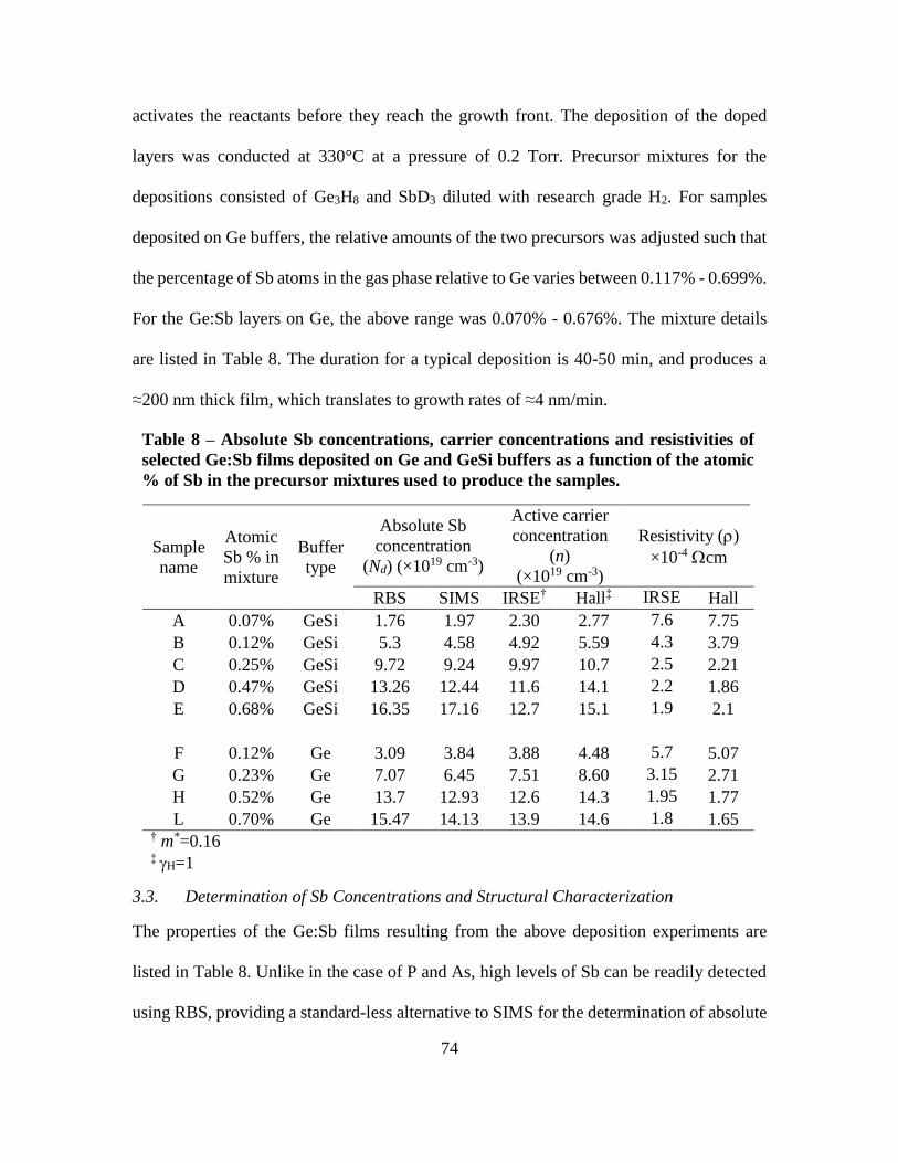
74
activates the reactants before they reach the growth front. The deposition of the doped
layers was conducted at 330°C at a pressure of 0.2 Torr. Precursor mixtures for the
depositions consisted of Ge3H8 and SbD3 diluted with research grade H2. For samples
deposited on Ge buffers, the relative amounts of the two precursors was adjusted such that
the percentage of Sb atoms in the gas phase relative to Ge varies between 0.117% - 0.699%.
For the Ge:Sb layers on Ge, the above range was 0.070% - 0.676%. The mixture details
are listed in Table 8. The duration for a typical deposition is 40-50 min, and produces a
≈200 nm thick film, which translates to growth rates of ≈4 nm/min.
3.3. Determination of Sb Concentrations and Structural Characterization
The properties of the Ge:Sb films resulting from the above deposition experiments are
listed in Table 8. Unlike in the case of P and As, high levels of Sb can be readily detected
using RBS, providing a standard-less alternative to SIMS for the determination of absolute
Table 8 – Absolute Sb concentrations, carrier concentrations and resistivities of
selected Ge:Sb films deposited on Ge and GeSi buffers as a function of the atomic
% of Sb in the precursor mixtures used to produce the samples.
Sample
name
Atomic
Sb % in
mixture
Buffer
type
Absolute Sb
concentration
(Nd) (×1019 cm-3)
Active carrier
concentration
(n)
(×1019 cm-3)
Resistivity ()
×10-4 cm
RBS SIMS IRSE† Hall‡ IRSE Hall
A 0.07% GeSi 1.76 1.97 2.30 2.77 7.6 7.75
B 0.12% GeSi 5.3 4.58 4.92 5.59 4.3 3.79
C 0.25% GeSi 9.72 9.24 9.97 10.7 2.5 2.21
D 0.47% GeSi 13.26 12.44 11.6 14.1 2.2 1.86
E 0.68% GeSi 16.35 17.16 12.7 15.1 1.9 2.1
F 0.12% Ge 3.09 3.84 3.88 4.48 5.7 5.07
G 0.23% Ge 7.07 6.45 7.51 8.60 3.15 2.71
H 0.52% Ge 13.7 12.93 12.6 14.3 1.95 1.77
L 0.70% Ge 15.47 14.13 13.9 14.6 1.8 1.65 † m*=0.16 ‡ H=1

75
Sb contents in the thin films when the concentrations are above 2×1019 cm-3. Furthermore,
RBS channeling experiments provide an insight to whether the incorporated Sb occupies
substitutional or interstitial positions in the lattice. It was observed that for films with near
full activation listed in Table 8, similar degree of channeling was observed for both Ge and
Sb signals. An example RBS spectrum for a sample which was measured to have 0.28%
(1.24×1020 cm-3) incorporated Sb in the film is shown in Figure 15. The inset of the figure
shows the clear Sb signal that allows the determination of atomic concentration based on
modelling. The ratio between channeled and random spectra (χmin) for these samples does
not exceed 15%. But in samples with very high levels of incorporated Sb (Nd > 1.6×10²⁰
cm-3, not shown in the table), de-channeling of the Sb signal is observed with respect to the
Figure 15 - RBS spectra and composition fit for a sample containing 9.2x1019 cm-3
carrier concentration. The random and channeled spectra are shown by the black
dashed and blue colored lines respectively, whereas model fit is depicted by the red
line. The Sb content is fitted to be 0.28%. Both Ge and Sb signals are showing
excellent channeling, indicating full substitution. The inset is a close-up of the Sb
peak.

76
Ge, and χmin increases (>25%). The active carrier concentrations of these samples are
substantially lower than the total Sb concentrations, indicating that incomplete activation
arises from the donor atoms occupying interstitial sites.
SIMS measurements were also carried out on the above films using a CAMECA IMS 6f
instrument using a Cs+ primary beam. This allows a more accurate quantification to be
carried out in samples with lower Sb concentrations. The Sb atom concentrations obtained
by comparison with a Ge standard implanted with 5×10¹⁹ atoms/cm3 of 121Sb are presented
in Table 8, and are in good agreement with the RBS results within error of measurement.
In addition to corroborating the RBS data, the SIMS elemental profiles also reveal
extremely uniform dopant distribution within the doped layer, and an abrupt decrease of
the dopant atoms at the interface with the undoped portion of the film. This indicates the
lack of any diffusion effects even at the highest Sb concentrations, and can be attributed to
the ultra-low temperature deposition conditions. Figure 16 (a) depicts a typical SIMS
elemental profile obtained for a sample with an absolute Sb concentration of
1.24×1020 cm-3 grown on Ge0.95Si0.05 substrate exhibiting abovementioned features. The
arrangement of the various layers in this structure is depicted in Figure 16 (b). The
concentration of Sb obtained using SIMS for this sample agrees well with the 1.33×10²⁰
cm-3 value obtained via RBS.
In addition to diffusion of Sb to the substrate, another factor that is essential for obtaining
uniform dopant profiles is the absence of Sb segregation to the surface. In order to verify
this property for the SbD3 doped Ge, a film was capped by an intrinsic Ge layer, as
schematically depicted in Figure 16 (d). This capping layer was deposited immediately

77
after the Ge:Sb layer without removing the wafer from the growth chamber or subjecting
the surface to any cleaning procedure. If any Sb segregation occurs, an increase in the Sb
concentration should be evident at the interface between the doped layer and undoped
capping layer. As seen from the SIMS profiles for the above sample presented in Figure 16
(c), the Sb counts drop sharply from the value in the doped film down to background levels
at the interface. This indicates that the incorporated Sb is distributed uniformly in the doped
film, with no enhancement of concentration at the surface.
The microstructure of the Ge:Sb films was analyzed using XTEM and AFM, as depicted
in Figure 17 (a) and (b), respectively. The former technique reveals a flat, defect free n-
Figure 16 – (a) SIMS elemental profiles for a sample grown on Ge0.95Si0.05 buffered
Si, the schematic for which is shown in (b). The absolute Sb level in the doped layer
is 1.24×1020 cm-3. (c) SIMS profile for a 170 nm thick layer with 1.75×1020 cm-3 donors
which is capped with a 40 nm thick intrinsic Ge layer, as shown schematically in (d).
The interface between the doped and undoped regions is sharp, indicating that no Sb
has segregated to the surface despite Sb incorporation above the solubility limit in the
doped layer.

78
type epilayer, indicating that the growth is fully commensurate with the buffer layer, and
the large Sb atoms does not disrupt crystal assembly. This is especially remarkable given
that the epilayer depicted in Figure 17 (a) has a donor atom concentration of
1.05×1020 cm-3, and a thickness of 200 nm. The flat surface is corroborated by AFM
measurements which give a RMS surface roughness of <1 nm. A typical AFM from a
sample with a carrier concentration of 8.8×1019 cm-3 is given in Figure 17 (b).
In order to gain additional insights into the Sb incorporation and donor activation, the
lattice parameters of the doped films were measured using HRXRD. As in the case of As
doped films described in Section 3, an expansion of the lattice is evident at high dopant
levels. Figure 18 shows a series of (004) -2 scans from a set of doped samples which
illustrate the increase of the out of plane lattice parameter with increasing dopant
concentration. All the layers are grown on Ge0.95Si0.05 buffers which facilitate the
Figure 17 – (a) XTEM image of a Ge:Sb film (Nd=1.05×1020 cm-3) on a Ge buffered Si
substrate, with the interface between the doped and undoped regions marked by an
arrow. The n-type layer is defect free within the field of view, with a flat surface (b)
AFM image of Sb doped Ge film with an active carrier concentration of 8.8×10¹⁹ /cm3.
The RMS surface roughness calculated from this image is 0.97 nm.

79
determination of the epilayer peak position due to minimal overlap with the buffer peak.
Furthermore, since the epilayers are pseudomorphic to the buffer layers, they have the same
in plane lattice parameter. Therefore the increase in the out of plane lattice constant
observed in the figure corresponds to an increase in the relaxed lattice constant. This was
further verified by obtaining (224) reciprocal space maps of the epilayer and buffer layer
peaks. The in-plane and out-of-plane lattice constants can be measured using the maps, and
by applying standard elasticity theory, it is possible to calculate the relaxed lattice
parameter. The (224) RSM also enable the calculation of strains. The larger lattice
parameters of the doped films will lead to compressive strain if deposited on bulk Ge, the
tensile strain present in the Ge buffer layers opposes this effect, leading to largely strain
relaxed films. The films deposited on GeSi buffer layers do exhibit compressive strain due
to the greater lattice parameter difference in comparison to the substrate. However, in all
Figure 18 - θ-2θ scans for the 004 reflection in several Sb-doped Ge films grown on
Ge0.95Si0.05. The peaks at high angles correspond to the buffer layers. Figure adapted
with permission from Xu, C. et al. Phys. Rev. B 2016, 93 (4), 041201. Copyrighted by
the American Physical Society

80
cases the (224) RSMs revealed that the strains are small, and are therefore not expected to
affect the measurement of optical and electrical properties given here.
As a result of the work described thus far in this chapter, Ge films which are highly doped
with two different group V donor atoms –namely As, and Sb– which exhibit nearly
complete activation are now available. As discussed above, it is evident that the dopant
incorporation has a significant effect on the lattice parameter of Ge. Combined with the
data for similarly P doped Ge films provided in Reference 115, a detailed analysis of the
differences in manifestation of this phenomenon among different group V dopant atoms
allows the identification of the correct theoretical framework required for its description.
Such an analysis is presented in Reference 141, and it was found that the lattice expansion
could be described as a sum of contributions arising from electronic and size effects as
described by the Cargill-Keyes theory. This can be expressed mathematically as:
Da0
a0
= bNd = bsize + be( )Nd =2
a**NGe
DR
R-
ac
3B
æ
èçö
ø÷Nd
(4.2)
In the above equation, a0 is the change in the lattice constant, a0 is the lattice constant of
the undoped material, and Nd is the dopant concentration. The coefficient of change in
lattice parameter is denoted as , which is separated in to the contribution from donor atom
size (size)and electronic effects (e). The physical parameters that determine these
contributions are the topological rigidity parameter (a**=0.7 for diamond and zinc blende
semiconductors),152,153 relative difference between the donor-Ge and Ge-Ge bond lengths
for an isolated donor (R/R, calculated to be 0.0674 for the Ge-Sb case by Chizmeshya et
al. in Ref. 80), the bulk modulus (B=4.682×10²³ eV/cm3=75.01 GPa from Ref. 154), the

81
atomic density of bulk Ge (NGe=4.418×1022 cm-3), and the absolute deformation potential
for the conduction band states (ac). The latter is calculated to be ac = -1.5 eV by Van de
Walle,155 which compares well with the values given in References 156 and 157.
Figure 19 compares the lattice paramters calculated using Equation 4.2 with the
experimantal lattice parametrs observed for samples with 1.0×1019 cm-3 < Nd < 1.6×10²⁰
cm-3. As noted earlier, these samples show excellent channeling of the RBS Sb signal
which indicates substitutional incorporation of the donor atoms in the lattice. The fact that
the experimental lattice parameters agree well with the theoretical predictions for Ge:Sb
with full substitutional donor incorporation further validates the above conclusion, which
can be used to explain the electrical properties of these films, presented below.
Figure 19 – Plot of the experimental relaxed lattice parameter determined from (224)
RSMs vs. the total Sb content determined from RBS. The solid line is the calculated
lattice parameter based on Cargill-Keyes theory as described in Equation 4.2. The
light and dark shaded areas respectively represent the size and electronic
contributions to the lattice expansion.

82
3.4. Electrical Properties of Ge:Sb Films – Carrier Concentration
The active carrier concentrations of the films listed in Table 8 were determined using both
IRSE and Hall measurements. The former were conducted on a J. A. Woollam IR-VASE
ellipsometer, while the latter measurements were made using an Ecopia 3000 Hall system.
It can be seen that when the customary Hall factor of H=1 is used, carrier concentrations
are found to be greater than donor concentrations, which is unphysical. This discrepancy
is resolved if a Hall factor H=0.87 is used, which is obtained by assuming Nd = n for
concentrations up to 1.0×1020 cm-3. This assumption can be validated by the Altermatt
model for frustrated incomplete donor ionization as applied for the Ge case in Reference
135, and the Hall factor agrees well with the theoretical estimate of H=0.83.158,159 Best
agreement of the Hall and ellipsometry results can be obtained when the effective mass
value of m*=0.16m is used. This is in contrast to the m*=0.120m value used for the Ge:As
films earlier. Such systematic differences may indicate a donor-dependent Hall factor or
effective mass.
The carrier concentrations obtained from this analysis is plotted in Figure 20, and it can be
seen that for high donor concentration in the 1.2×1020 cm-3 > Nd > 1.6×1020 cm-3 range, the
carrier concentrations deviate from the complete ionization predicted by the Altermatt
model. While it is possible to incorporated more Sb up to concentrations of 1.2% (5.3×10²⁰
cm-3), this does not result in a further increase in the active carrier concentrations. However,
below the 1.6×1020 cm-3 limit, structural data presented earlier suggests that full
substitutional donor incorporation occurs. This trend is in agreement with the electrical
properties of the films, will be discussed in greater detail in the context of resistivity values
presented below.

83
3.5. Electrical Properties of Ge:Sb Films – Resistivity
The resistivity values given in Table 8 are plotted with respect to active carrier
concentrations in Figure 21. The solid line in Figure 21 is a fit to the bulk Ge:Sb data
compiled by Cuttriss, shown as black circles in the plot. The fit is of the form
𝜌 =1+(
𝑛
𝑛0)𝛼
𝜇𝐿𝑛𝑒 (4.1)
Where n0 and are adjustable parameters and L=3800 cm2/Vs is the lattice contribution
to the electron mobility. This expression was proposed by Hilsum,144 and was used earlier
in a similar fit of the date obtained for Ge:As films in the previous section. In that instance,
it was found that =0.5. However, for Ge:Sb films, the fit parameters =0.39 and
n0=9.21×1016 cm-3 provides the best fit shown in the figure. The resistivity values obtained
from ellipsometry and Hall measurements for the films doped using SbD3 are shown as
Figure 20 - Experimental carrier concentrations n as a function of the measured
donor concentrations Nd in Ge:Sb films. The solid line is a prediction based on
Altermatt’s model of incomplete ionization.

84
dark and light squares respectively in the same plot. For consistency with the literature
data, a Hall factor of H=1 is used in the comparison, and it can be seen that the resistivity
values are in good agreement with the extrapolation from bulk values to the much higher
carrier concentrations in the SbD3 doped samples.
The resistivity values are compared to those reported by Oehme et al. and Thareja et al. for
similar carrier concentrations. The trends show that only prior study that reports film
resistivity comparable to bulk Ge is that by Thareja et al.,148 in which Sb implanted samples
were produced and laser annealed at the melting point. In this case carrier densities up to
2x10²⁰ /cm3 were measured but the corresponding resistivity is higher than expected from
our observations as shown in the figure. Collectively the results above indicate that the
Ge:Sb films doped with SbD3 have superior structural properties that result in record low
Figure 21 – The resistivity values (dark and light squares denote values obtained
from ellipsometry and Hall measurements, respectively) from Ge:Sb films doped
with SbD3 compared with bulk data compiled by Cuttriss (solid circles).145 The solid
line is a Hilsum144 fit to the Cuttriss data. Literature values from Oehme et al.147 and
Thareja et al.148 are also included for comparison.

85
resistivities. Indeed, the lowest resistivity value of 1.8×10⁻⁴ Ωcm is the best reported thus
far in literature. It is interesting to note that the lowest resistivities are observed in the
highest doped samples in the 1.4×1020 cm-3 < Nd < 1.6×1020 cm-3 range, for which it appears
not all donors are fully active. However, RBS channeling experiments indicate that the Sb
atoms in these samples occupy substitutional positions. As mentioned earlier, for Nd >
1.6×1020 cm-3, the active carrier concentrations decrease and this is accompanied by an
increase in the channeling yield (χmin) in the RBS spectra. Donor-vacancy clusters, which
have been shown to form preferentially in Ge:As and Ge:Sb, may be the cause of this donor
deactivation.160,161
3.6. Doping Efficiency
The measurement of absolute Sb concentrations reveal that the incorporation of Sb via
SbD3 is highly efficient, with the Sb/Ge ratios of the precursor mixtures being equal to the
Sb/Ge ratios of the deposited films at low doping levels. Even at high doping
concentrations, the latter value is ≈50% of the former, as seen from the precursor and film
Sb concentrations given in Table 8. This observation also supports the conclusion that all
of the incorporated Sb is active, since no extra Sb is available to be in an inactive form.
This is in contrast to the As(SiH3)3 and As(GeH3)3 precursors described earlier, where a
greater portion of the dopant precursor does not contribute to dopant incorporation in the
film. Indeed, SbD3 has higher incorporation ratio compared to the molecules in the
D(MH3)3 family (D=P, As; M=Si, Ge). This comparison is justified due to the essentially
identical methods used for the deposition of the doped films using various precursors. In
addition, a saturation point of donor activation is reached at ≈0.6% donor atoms in the
precursor mixture for all precursors, beyond which further increase in carrier

86
concentrations is not reached. These trends are illustrated in Figure 22. The more efficient
behavior SbD3/Ge3H8 combination is reminiscent of the SnD4/Ge3H8 precursor system
used for deposition of GeSn alloys. As discussed in Chapter 5, the compatible reactivity of
the two precursors allows depositions in which the film and precursor mixture element
stoichiometries are nearly equal. Overall, the plots presented above can be used as a guide
for incorporating target donor levels of P, As and Sb using novel low temperature
precursors discussed above. It must be noted that even though donor incorporation
efficiency of the D(MH3)3 molecules is less than SbD3, they are nevertheless superior to
the traditional PH3 and AsH3 sources. In addition, all of the abovementioned molecules
present an opportunity to develop environmentally safer alternatives to traditional in-situ
doping methods that utilize extremely toxic gaseous precursors.
Figure 22 – Efficiency of doping for P, As, and Sb doped Ge films synthesized using
single source CVD, which reveals SbD3 has higher incorporation efficiencies than
D(MH3)3 molecules.

87
From the donor activation and resistivity results presented above, it can be concluded that
the novel chemical approaches to doping Ge with group V donors described above not only
gave rise to technologically relevant highly doped semiconductor material, but also
contributed to expanding the understanding of the fundamental properties of doped Ge. To
extend this line of inquiry further, the properties of the double donor S in Ge was
investigated next.
4. Sulfur doping of Ge using Disilylsulfide and Digermylsulfide
4.1. Introduction
Due to the success of using molecules with pre-formed bonds between group IV and group
V atoms for the doping of Ge, this approach was next applied to the introduction of group
VI doping atoms into the Ge matrix. This was made possible by the S(SiH3)2 and S(GeH3)2
precursor molecules introduced in Chapter 2. The motivation for pursuing this research
avenue is the success obtained in doping Si to high levels with the group VI element S.
This produces the material known as ‘black silicon’ which has been used to demonstrate
prototype detector and solar cell devices.162–166 The achievement of high carrier
concentrations in this case is facilitated by the double donor nature of S. Similar
applications at longer IR wavelengths can be envisioned for S doped Ge, where the first
and second ionization energies are 0.28 eV and 0.59 eV respectively.118,167
The most common doping approaches for S doped Si to date include gas-phase diffusion
of elemental sulfur, traditional implantation followed by laser annealing of the wafers and
laser irradiations in an SF6 ambient.162,168–171 Most recently laser induced incorporation of
S via overpressures of gaseous SF6 has been reported to produce reasonably high amounts
of S (5x1019 cm-3) although the degree of their activation is limited to 1%.172 A common
88
issue in conventional synthesis techniques is the inability to precisely control the spatial
and depth distribution of the S atoms and the inherent compositional non-uniformity with
respect to the substitution of single S atoms or S2 dimers in the target lattice.167,170,171 In
spite of this limitation intriguing optical physics have emerged from the pioneering work
in this nascent semiconductor material arena including combinations of deep impurity as
well as shallow donor levels. These fundamental discoveries have demonstrated potential
for the design and development of possible device structures based on black silicon.
In the case of Ge, S doping has also been achieved by physical methods, including
diffusion173 and implantation.174–176 An important area of application is the modulation of
Schottky barrier heights at metal-Ge interfaces. In addition, since Ge is the material of
choice for near-IR photodetector in the flourishing area of Si photonics, this S doping
approach may also represent a direct and reproducible route to crystalline n-type Ge-on-Si
layers for applications in a wide range of new device platforms, including Ge based
lasers.10 Several related reports also emerged of S doping in structurally compatible III-V
systems, such as InP and GaAs, although these studies appear to be of a preliminary nature.
Finally, and presumably because of its possible analogy to black silicon, S doped Ge has
been mentioned in the patent arena, but without disclosure of specific methodologies for
producing such materials.177
For actual device application the processing of doping semiconductors typically requires
control of both uniformity of composition and amount of dopant that is incorporated into
the growing film. In the case of sulfur in Si this is difficult to attain using most obvious
sources such as H2S and metal-organic analogs since these require growth and processing

89
at high temperature which precludes a substantial degree of dopant atom activation.
Another issue is the propensity of introducing undesirable contaminants impacting the
quality of the final material. To circumvent some of these issues here we propose an
entirely new approach to achieve in situ doping during growth of group IV heterostructures
using purposely designed molecular sources such as S(SiH3)2 and S(GeH3)2 that exhibit
the required reactivity and structural compatibility with the parent diamond lattice. In the
case of both of these molecules the S atom is pre-bonded to group IV atoms terminating
with easily removable hydrogen ligands which can be readily eliminated as highly stable
H2 leaving behind SSi2 and SGe2 core structures with bonding properties akin to those
present within the bulk group IV crystal. The bonding arrangements of the incorporated
cores also strongly promote “automatic” activation of substitutional S atoms by virtue of
the near tetrahedral electron domain geometry of their S central atoms. In addition these
configurations are expected to suppress S-S near neighbor bond formation further
increasing the electronic homogeneity of the active site distribution in the crystal.
Although, to our knowledge, this strategy has not been implemented in S doped Si it has
the potential to circumvent the deleterious effects that the diffusion and implantation may
have on the crystalline properties of the final product. Since Ge is the material of choice
for near IR photodetector in the flourishing area of Si photonics, this S doping approach
may also represent a direct and reproducible route to crystalline n-type Ge-on-Si layers for
applications in a wide range of new device platforms including Ge-based lasers.
To test the viability of our approach using S(SiH3)2 and S(GeH3)2 as sulfur delivery agents
we adopted Ge films grown on Si as the candidate host material for our studies. The
molecular cores of these compounds are structurally compatible with bond lengths in

90
germanium, making this lattice an ideal test bed, as corroborated by ab initio
calculations.118
4.2. Growth of Ge:S layers on Si(100) using Digermylsulfide and Tetragermane
As a feasibility experiment we attempted minimally doping Ge films with S atoms in the
1018 target range which still represents a sufficient number of atoms to ensure full
activation. The films were grown on 4 inch Si(100) high resistivity wafers via reactions
of S(GeH3)2 and Ge4H10 using a single wafer gas source MBE reactor described
elsewhere.77 The substrates were first dipped in HF to remove the native oxide layer and
then heated on the sample stage at 550 oC for 5 minutes under ultra-high vacuum to desorb
residual impurities and generate an epitaxy-ready surface as evidenced by in situ RHEED
analysis. Crystal growth was commenced by inserting the gaseous mixture into the
chamber through a nozzle terminating with a showerhead which was positioned at a
distance of 3” from the substrate surface. The gas flow was controlled by a high precision
needle valve and the growth pressure was maintained constant at 10-4 Torr via dynamic
turbo-pumping. The wafer-heater temperature was kept constant at approximately 380 oC
for all experiments while the reaction times varied from 25-40 minutes from sample to
sample. The corresponding average growth rates were found to be in the range of 10 to
12.5 nm/min presumably due to slight deviations in S(GeH3)2 flux concentration. It is
interesting to note that under similar conditions the Ge4H10 compound has been previously
shown to produce device quality Ge-on-Si films with large thicknesses of several microns
and beyond using a comparable low temperature range of 380-400oC yielding
commercially viable growth rates approaching 30 nm/min. We see that the latter rates are

91
2-3 times higher than those obtained in this study indicating that the presence of S(GeH3)2
at the growth front significantly reduces the reaction kinetics for the Ge:S films.
Table 9 contains a summary of the Ge:S film parameters including thickness, active carrier
concentrations and mobility values determined by Hall and the absolute amount of S
incorporated in the film as measured by SIMS. The thicknesses was determined by
spectroscopic ellipsometry and corroborated by RBS which was also used to show that the
samples were fully commensurate to the substrate by measuring the ratio of the channeled
and random signals in the spectra (connoted as min). The RBS analysis yielded min values
as low as 5-10 % indicating a high level of film-crystal alignment with the wafer. High
resolution XRD confirmed the single crystal character of the layers and indicated that they
typically possessed residual compressive strains on the order of 0.15 % which were readily
relieved by rapid thermal annealing at 600-700oC. Further characterizations by XTEM
revealed uniform mono-crystalline films possessing epitaxial hetero-interfaces and
atomically flat surfaces indicating that the incorporation of sulfur does not significantly
disrupt the high microstructural quality of the Ge layers as shown in Figure 23.
Table 9 - Summary of S-doped Ge film parameters produced using S(GeH3)2 . The
data includes thickness, SIMS and Hall concentrations as well as mobility values
of the post-annealed samples.
No.
RBS
thickness
(nm)
As-grown
Hall (cm-3)
Annealed
Hall (cm-3)
SIMS conc.
(cm-3)
Post-anneal
mobility
(cm2/(Vs))
001 300 3×10¹⁷ 4×10¹⁷ 1×10¹⁷ 530
003 400 8×10¹⁷ 7×10¹⁷ 4×10¹⁷ 750
007 400 3×10¹⁷ 3.3×10¹⁷ 2×10¹⁷ 830
008 500 3×10¹⁷ 3×10¹⁷ 1×10¹⁷ 960

92
All of the samples described in Table 9 were grown using one liter gaseous reaction
mixtures comprising room temperature vapor pressure of Ge4H10 (1.6 Torr) and varying
amounts of the S(GeH3)2 co-reactant ranging from 0.50 Torr (sample 001) to 1.8 Torr
(sample 003, 007 and 008) diluted with high purity H2. Samples 003, 007, and 008 were
all grown at 380oC within a time frame of 40 minutes. However, the flux concentration of
008 was slightly higher than that of 003 or 007 thus increasing the growth rate and yielding
a thicker corresponding film, as expected. We find that among these samples 003 contains
8x10¹⁷/cm3 active donor carriers while a similar but slightly lower value of ~ 3x10¹⁷/cm3
is found for sample 007 and 008 as determined by the Hall method. It is interesting to note
that the average amount of active S incorporated in these three samples after annealing is
~ 4 x 10¹⁷as measured by Hall with inherent variations that may arise due to slight
fluctuation of the growth conditions during deposition. For example we find that the
threshold temperature for reaction of the dominant Ge4H10 source is within the narrow
Figure 23 - XTEM micrograph of S doped Ge layer grown upon Si(100) at 380oC via
reactions of S(GeH3)2 and Ge4H10. Inset shows a high-resolution image of the
interface marked by the arrow.

93
range of 380 to 390 oC leading to a sharp rise in deposition rates within this temperature
window. In this context the slightly reduced S incorporation in sample 008 relative to 003
and 007 may then be explained by a the inherent decomposition of the Ge4H10 at the above
temperature combined with the higher concentration of the reactants (lower dilution)
employed for this sample. Sample 001 was grown using a significantly shorter deposition
time or 25 minutes which accounts for the reduced thickness of the films. Interestingly in
spite of the decrease in concentration of the S(GeH3)2 co-reactant in the growth flux of 001
the degree of S incorporation is comparable to the average of the other samples as
determined by Hall.
The amounts determined by Hall represent the activated values of the dopant and has
important implication for device applications. From a sample preparation perspective
using a new protocol it is crucial to establish the actual amount of S contained in the film.
For this purpose we conducted SIMS analysis using an implanted 300 nm thick sample
containing 1x10¹⁹ S atoms/cm3 as a standard. Compositional profiles were acquired using
a Cameca-6F SIMS instrument and the data showed a uniform distribution of both S and
Ge atoms throughout the bulk films listed in the table. In all cases the absolute S amounts
measured by SIMS are found to be consistently smaller by a factor of 2-3 compared to the
activated concentrations obtained from Hall. Given that our pure reference Ge films grown
under the same conditions are p-type with 5x1016 cm-3 acceptor levels, the n-type character
of our doped films provides strong evidence that S atoms must be both incorporated and
activated. Although their concentration is small and may in some cases (samples 001 and
008) approach the detection limit of the instrument, the consistency in the procedures used
makes the doubling of the ratio in the samples significant even though the absolute values

94
have large uncertainties. In fact Hall measurements on films 003 and 008 yield values of
~8 x10¹⁷/cm3 and ~3 x10¹⁷/cm3 whose ratio of ~2 is similar to that found in our SIMS
concentrations. Since sulfur can be viewed as double donor the lower value of the atomic
SIMS concentrations are expected to be lower by a factors of 2 as observed in the table, as
can be expected for fully ionized double donors. These initial results are encouraging and
indicate that S can be incorporated into Ge and hopefully these levels can be controlled by
adjusting the process conditions. Finally we note that the above data were obtained from
samples annealed via rapid thermal methods (RTA), which essentially showed no
significant change in active levels and SIMS contents compared to those of the as-grown
counterparts. However, as expected, the annealing essentially doubles the mobility from
sample to sample, which is consistent with the improvements in crystallinity afforded by
the RTA step and evidenced by XTEM and XRD characterizations. This is corroborated
by the observation that the highest mobilities are observed in the thickest samples, which
is consistent with increasing the volume fraction of defect-free material in the film (e.g.,
portion of the film not influenced by the highly dislocated interface region).
In spite of changes in concentration of S(GeH3)2, disparities in the ratio of co-reactants
used, and growth rates obtained, the resultant films have very similar doping properties
including comparable amounts of activated and incorporated S atoms. Thus the
concentrations listed on Table 9 can be viewed as the upper bound for fully substitutional
S for this family of samples. Therefore it appears that the reaction of S(GeH3)2 rejects the
additional sulfur supplied by greater reactant flux, which desorbs as some form of volatile
hydride, and ultimately results in a film devoid of undesirable interstitials or segregated
impurities. Collectively, the strategy developed here for the systematic incorporation
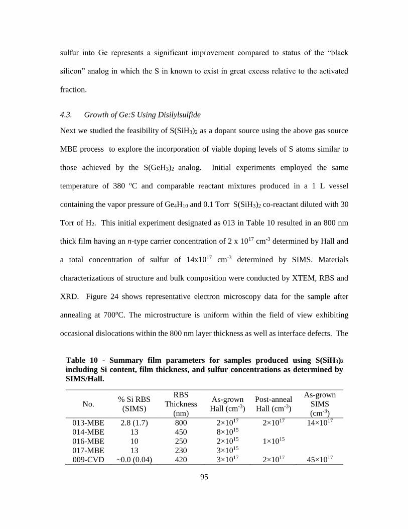
95
sulfur into Ge represents a significant improvement compared to status of the “black
silicon” analog in which the S in known to exist in great excess relative to the activated
fraction.
4.3. Growth of Ge:S Using Disilylsulfide
Next we studied the feasibility of S(SiH3)2 as a dopant source using the above gas source
MBE process to explore the incorporation of viable doping levels of S atoms similar to
those achieved by the S(GeH3)2 analog. Initial experiments employed the same
temperature of 380 oC and comparable reactant mixtures produced in a 1 L vessel
containing the vapor pressure of Ge4H10 and 0.1 Torr S(SiH3)2 co-reactant diluted with 30
Torr of H2. This initial experiment designated as 013 in Table 10 resulted in an 800 nm
thick film having an n-type carrier concentration of 2 x 1017 cm-3 determined by Hall and
a total concentration of sulfur of 14x1017 cm-3 determined by SIMS. Materials
characterizations of structure and bulk composition were conducted by XTEM, RBS and
XRD. Figure 24 shows representative electron microscopy data for the sample after
annealing at 700oC. The microstructure is uniform within the field of view exhibiting
occasional dislocations within the 800 nm layer thickness as well as interface defects. The
Table 10 - Summary film parameters for samples produced using S(SiH3)2
including Si content, film thickness, and sulfur concentrations as determined by
SIMS/Hall.
No. % Si RBS
(SIMS)
RBS
Thickness
(nm)
As-grown
Hall (cm-3)
Post-anneal
Hall (cm-3)
As-grown
SIMS
(cm-3)
013-MBE 2.8 (1.7) 800 2×10¹⁷ 2×10¹⁷ 14×1017
014-MBE 13 450 8×10¹⁵
016-MBE 10 250 2×10¹⁵ 1×10¹⁵
017-MBE 13 230 3×10¹⁵
009-CVD ~0.0 (0.04) 420 3×10¹⁷ 2×10¹⁷ 45×1017

96
free surface shows roughness undulations presumably originating from the initially high
sulfur levels incorporated in the as-grown material as shown in Table 10. This is in contrast
to pure Ge films grown under similar conditions which are found to possess planar
morphologies in all cases. The RBS spectra reveal small amounts of substitutional Si on
the order of ~ 2-3 % which is consistent with the 2.8 % value obtained by XRD
measurements of the lattice constant in conjunction with Vegrad’s Law. The XRD/RBS
plots also show that layers are largely devoid of epitaxial strains and are
crystallographically aligned with the underlying substrate (see Figure 24).
Figure 24 - (top left) XTEM micrograph of 800 nm thick Ge/Si(100) sample doped
with S. The Ge layer contains sporadic dislocations scattered across the film and
exhibits surface undulations. (top right) Corresponding random RBS spectra show
the main Ge peak and a very low intensity shoulder corresponding to Si (marked by
arrow). The channeled spectrum (red trace) indicates a high degree of epitaxial
alignment. (Bottom right) HRXRD plots of the 004 peaks and 224 reciprocal space
maps indicate that the layer is monocrystalline and virtually strain free. The
measured lattice constant is used to estimate the Si content at 2.8 % following
Vegard’s Law.

97
The S and Si content for sample 013 were measured by SIMS to be 14x1017 cm-3 and
7.6x1020 cm-3 (1.7%), respectively. The latter value is in reasonable agreement with the
XRD/RBS estimates given the large uncertainty with these techniques. The SIMS
concentration in this sample were obtained using implanted reference standards and
elemental profiles as shown in Figure 25 which also illustrates that the Si, and S atoms
furnished by the S(SiH3)2 compound are evenly distributed across the 800 nm thick layer.
In view of the order of magnitude discrepancy between the activated Hall value (2x10¹⁷
cm-3) and absolute (14x1017 cm-3) amounts of S in this sample determined by SIMS, we
attempted to increase the charge carriers via RTA processing of the samples up to ~ 700oC
for 5 seconds 3 times. In this case the number of carriers measured by Hall remained
essentially unchanged at 2x1017 cm-3. However, SIMS elemental profiles showed that the
total sulfur concentration after annealing was highly uniform and with a nominal level of
6.1x1017 cm-3 which is a factor of 2 lower than the corresponding as-grown value
(14x1017cm-3). Perhaps more importantly the above data shows that the Si content relative
to that of S in the sample is ~ 102 times higher than the 2:1 ratio inherent to the molecular
S(SiH3)2 delivery source. This indicates that under these conditions the precursor likely
disproportionates to give volatile H2S or HS(SiH3) species, which desorb and therefore do
not participate in the growth, and highly reactive SiH2 radicals that remain at the growth
front and eventually incorporate Si into the film as shown by the equations:
S(SiH3)2 SH(SiH3) + SiH2 H2S + 2 SiH2 (4.3)
SiH2 Si + H2 (4.4)

98
To mitigate the aforementioned process depicted by equations (4.3) and (4.4) we next
systematically lowered the deposition temperatures to 370, 360 and 350 oC to produce
samples 014, 017 and 016, respectively. However, in all three experiments we found that
the active carrier concentrations were in fact further reduced to levels below the SIMS
detection threshold in the range of 1015 cm-3 measured by Hall. The latter value is opposite
in sign and lower in magnitude than the intrinsic 5x1016 cm-3 p-type level of reference Ge
grown using the same Ge4H10 precursor indicating that the dopant has overcompensated to
yield n-type material further supporting our assertion that sulfur is being incorporated even
under the foregoing reactions conditions. In contrast to the lowering of the S substitution
under the above conditions we find that the Si content in the materials increases
dramatically to the 10-13 at % range as measured by RBS and XRD. These films therefore
represent true Si1-xGex alloys containing only trace amounts of sulfur as further evidenced
by the anomalously large mobility (>1200 cm2/Vs) measured in the as grown samples. The
unexpected outcome of experiments 014, 016 and 017 suggest that the reactivity of
S(SiH3)2 is significantly higher than that of the dominant Ge4H10 source within this lower
Figure 25 - SIMS elemental profile of the as-grown sample 013 showing uniform
distributions of Si and S atoms throughout. The corresponding concentrations are
measured to be 7.6x10²⁰ and 1.4x1018 cm-3 using implanted standards.

99
temperature window (350-380oC). This is manifested by a five-fold increase in growth
rate observed for sample 013 (15 nm/min at 380oC) compared to samples 016 (3 nm/min
at 350oC). A concomitant increase in the incorporation of Si in the films by a similar factor
of ~5 is obtained for the lower rate film, as expected. This lends support to the
decomposition mechanism proposed above (see equations) to explain the high Si content
relative to that of S for the 380oC deposition.
In view of this issue with the single-wafer MBE viability of the S(SiH3)2 doping process
we also explored an alternative UHV-CVD strategy which may provide a more rigorous
composition control of the Si and S co-dopant atoms using the same S(SiH3)2 reactant. The
process involves preheating the chemical sources to promote the activation and gas phase
interactions among the co-reactants thereby increasing the likelihood of intact
incorporation of the corresponding molecular Si2S cores into the target material. Here we
adopted previously described UHV-CVD protocols which are known to produce device
quality Ge layers by adding a small flux of SnD4 into the reaction stream to yield Ge film
doped with Sn in the range of 1019-1020 cm-3. The role of Sn is to promote layer-by-layer
assembly of highly crystalline films with low dislocation densities and flat surfaces by
suppressing the classic Stranski-Krastanov growth mode in which the crystal is formed by
island coalescence. We note that the isovalent Sn dopant levels do not change key materials
characteristics including lattice parameters, electronic structure and electrical properties.
A series Ge film was grown using one-liter mixtures of SnD4 (0.12 Torr), S(SiH3)2 (0.73
Torr) and 54 Torr of Ge2H6 diluted by 600 Torr of H2 (a representative material referred to
here as sample 009 is listed as the last entry in Table 10). The reaction temperature was

100
390oC and the working pressure was 0.300 Torr. Under these conditions high quality Ge
on Si layers were produced with thickness of 400-450 nm as evidenced by RBS, XRD.
SIMS profiles showed uniform distributions of S and Si with concentrations of 4.5x10¹⁸
cm-3 and 1.7x10¹⁹ (0.04 % Si), respectively, corresponding to a 1:3.5 atomic ratio. The
latter is within error of the expected factor of 2 based the SSi2 content of the molecular
cores indicating that they may be largely incorporated intact into the lattice thus providing
a good level of compositional control as anticipated. Hall measurements gave n-type
carrier concentrations of 2.5x1017 cm-3 in the as grown films which remained essentially
unchanged upon annealing at 600-700oC for 10s 3 times. When the samples were annealed
at 700oC, Hall measurements showed a p-type carrier concentrations similar to that of
intrinsic levels in Ge reference layer grown under same protocols indicating that the S
atoms no longer occupied substitutional lattice sites. In light of this result it is instructive
to compare this CVD sample (009) and the previously discussed MBE sample (013) which
were both found to have similar active S contents ~ 2x1017 cm-3 by Hall and one order of
magnitude higher via SIMS. The most striking difference between these two samples is
that the Si content is several orders of magnitude greater in the MBE sample 013 than in
the CVD sample 009. Since the latter CVD samples lose virtually all S donors and switch
from n- to p-type when annealed at 700oC while the S composition and dopant type of the
corresponding MBE films remained unchanged up to at least 800oC, our finding suggests
that excess Si in sample 013 may be responsible for the apparent stability of the S sites in
a Ge lattice.
The apparent stabilizing effect of Si with respect to S dopants and the consistency of
incorporated S levels in the S(GeH3)2 grown samples are intriguing results which are best
101
explored from a theoretical perspective. Accordingly, density functional theory (DFT)
calculations were carried out with the main goal of investigating the mutual defect
interactions among S atoms, Ge vacancies and substitutional Si atoms on the Ge crystal.
The results of these studies are presented in Reference 118, and reveal that doping using
S(GeH3)2 results in the formation of both substitutional and non-substitutional S defect
clusters, allowing the high level of activation observed in these samples. In contrast, doping
using S(SiH3)2 leads to near substitutional defect clusters that act as deep donors and result
in lower levels of activation.
The above results demonstrate the feasibility of using S(GeH3)2 and S(SiH3)2 sources for
S doping of Ge, and explore fundamental aspects of donor incorporation and activation
using these precursors. However, it must be noted that this preliminary study did not
encompass the growth of doped Ge films on Ge buffered Si substrates under UHV-CVD
conditions using Ge3H8 as the Ge source. The latter deposition method was used
successfully in combination with As(GeH3)3, As(SiH3)3 and SbD3 donor sources to produce
doped Ge films, as described in previous sections. Future studies employing this technique
to produce S doped Ge films may be able to achieve higher levels of active S incorporation
than is reported here.
5. Conclusion
In this chapter, fabrication of n-type doped Ge thin films was described. The target was to
achieve heavily doped films with active carrier concentrations >5×1019 cm-3 as required
for Ge based FET and laser applications. For As donors, the synthetic approach utilized for
incorporation of the target atoms was to use As(GeH3)3 molecules which have been

102
previously investigated for doping of GeSn alloys. The high reactivity of this compound
allows depositions to be conducted at low temperatures which results in incorporation of
donors at high concentrations of 8×1019 cm-3. In addition, the analogous silyl compound
As(SiH3)3 was also investigated as a dopant source. This compound were found to have
comparable behavior to the germyl analog, and the films doped using it have similar
electrical and structural properties. This data, in conjunction with the minimal degree of Si
incorporation as indicated by SIMS, indicates that using the silyl analogs does not have a
detrimental effect on the doped Ge films. Therefore As(SiH3)3 present a favorable
alternative for As(GeH3)3 in an industrial setting, due to its superior thermal stability and
greater volatility. Comparing the active carriers with the elemental donor concentrations in
the films, it is found that great majority of the atoms are active, and therefore the resultant
electrical properties are similar to what is observed in bulk doped Ge.
For doping of Ge with Sb, the reactive hydride SbD3 was employed to conduct low
temperature, non-equilibrium doping. This allowed the deposition of films with ultra-high
levels of active donors up to 1.6×1020 cm-3, and resistivities as low as 1.8×10⁻⁴ cm. The
latter resistivity values are the lowest reported thus far for n-type Ge, and agree well with
extrapolation of resistivity values of bulk Ge:Sb to high carrier concentration observed
here. The low resistivity values for Sb agree with the order of ρSb < ρP <ρAs observed for
bulk Ge by Spitzer, Trumbore, and Logan,116 and also with theoretical predictions by Ralph
et al.146
The Ge films produced in this work was also used to elucidate certain fundamental physical
properties of heavily doped Ge. This includes confirmation of the Cargill-Keyes model for

103
the effect of donors on the lattice parameter of Si and Ge (see Reference 141). The donor
activation studies of As and Sb also confirm the frustrated donor ionization first observed
in P.135
Finally, the concept of using precursors with pre-formed donor-host atom bonds to enable
low temperature doping was extended to include S doped Ge. In these experiments, the
molecular sources S(GeH3)2 and S(SiH3)2 were employed for the fabrication of Ge:S films
for the first time. Films with carrier concentrations in the 1015 – 1018 cm-3 range were
experimentally demonstrated.
The techniques developed in this chapter present an important and novel pathway for
fabricating heavily doped Ge films with controlled dopant profiles and junction depths as
required for NMOSFET and optical applications. They underscore the importance of
selecting compatible precursor combinations when preparing semiconductor films with
extreme properties using CVD methods. Further optimization of the protocols developed
in this work can potentially improve the levels of doping observed here, paving the way
for new application areas.

104
CHAPTER FIVE
Growth of Germanium-tin Alloys on Ge Buffered Si Substrates
Synopsis
In this chapter, the deposition of Ge1-ySny alloys in the y=0.01-0.11 composition range on
Ge buffered Si substrates is described. For y≤0.06, Ge2H6 and SnD4 were used as the
precursors, and for y>0.06, Ge3H8 was used in combination with SnD4. Thick (~1 μm),
largely relaxed films with low dislocation densities were produced. The microstructure and
strain relaxation properties of GeSn alloys on this novel platform were studied.
Portions of this chapter were reprinted from Senaratne, C. L.; Gallagher, J. D.; Jiang, L.;
Aoki, T.; Menéndez, J.; Kouvetakis, J. Ge1-ySny (y=0.01-0.10) alloys on Ge-buffered Si:
Synthesis, microstructure, and optical properties. J. Appl. Phys. 2014, 116 (13), 133509
with the permission of AIP Publishing.
1. Introduction
The range of hydride precursors outlined in Chapter 2 contain compounds that can supply
Ge and Sn atoms and serve as the basis from which the GeSn alloys can be synthesized, as
well as other species enabling the extension of the electrical and optical properties of this
semiconductor system. In this chapter, the focus will be on how the germanium precursors
Ge2H6 and Ge3H8, which together with the Sn source SnD4, were used for the fabrication
of Ge1-ySny alloys in a wide range of compositions y=0-0.11 on Ge buffered Si platforms.
As described in Chapter 1, the Ge2H6 and SnD4 were first utilized for the growth of
GeSn alloys by Bauer et al.,50 whereas the Ge3H8/SnD4 combination was first investigated
by Grzybowski et al.91,94 A major milestone achieved by using high-order Ge hydrides

105
together with SnD4 was the demonstration of the first LED devices employing Ge1-ySny,
which had active layer Sn contents up to y=0.02.21 Also of note is the first observation of
PL from GeSn thin films.74
All of the above results were obtained using GeSn alloys deposited directly on Si(100)
substrates. The deposition of GeSn on Si must overcome the difficulties posed by the 4%
(and higher) lattice mismatch between film and substrate. To avoid island formation,
growth must be initiated at very low temperatures, which introduces a very high density of
defects. In the case of Ge on Si, substantial improvements in film quality can be obtained
by ramping up the growth temperatures and by applying high-temperature post-growth
thermal annealings.103,104,178–180 Unfortunately, these solutions are of limited value for the
GeSn system. Increases in growth temperature lead to lower Sn incorporation, and the
temperature range for post-growth annealing is reduced by the possibility of Sn
segregation.51,181 These limitations reduce the ultimate film thickness that can be achieved
and preclude the optimal elimination of defects, with considerable impact on the optical
properties. In particular, optical emission can be strongly suppressed in thin, highly
defected films. In Ge-like materials such as GeSn, film thickness is a particularly important
consideration because the diffusion length of electron-hole pairs can be as high as 0.4
mm,182,183 so that the non-radiative recombination velocity at the film/Si interface will
affect the overall emission intensity. These considerations suggest that there is significant
room for improvement of these signals if the materials issues can be properly addressed.
Therefore in this chapter Ge buffered Si was explored as a platform on which strain relaxed,
device quality, low defectivity GeSn alloys could be fabricated using the Ge2H6/SnD4 and

106
Ge3H8/SnD4 precursor combinations. This chapter will describe the protocols developed
for this purpose, and will also present results from investigation of the microstructure and
strain relaxation of the resultant materials. In the following chapter, their superior optical
properties are also discussed, which provide the motivation for fabrication of LED devices
on virtual Ge substrates, as described in Chapter 7.
2. Ge buffered Si Substrates – Significance and Fabrication Methods
Germanium provides a facile platform for the growth of GeSn alloys due to the relatively
small lattice mismatch between the substrate and the alloy epilayer. Therefore it has been
used as a substrate material from the early days of research on GeSn.28,30 Furthermore, the
band alignment between Ge and GeSn is known to be type I, which promotes carrier
confinement in the alloy layer. However, using Ge wafers for this purpose has the obvious
disadvantage that it excludes the possibility of integration of GeSn based materials on to
Si platforms for microelectronic and photonic applications. In order to circumvent this
issue while still retaining the advantage of a substrate material with low lattice mismatch
for the growth of GeSn alloys, Ge buffered Si substrates -also known as virtual Ge
substrates- were recently investigated by Vincent et al.51 Further work on GeSn alloys
deposited on Ge/Si has led to the successful fabrication of LED devices by several
groups.45,71,184 Despite these advances, several areas were identified as requiring further
development in order to fabricate functional direct gap light emitting devices. Firstly, the
alloys of the devices grown on Ge/Si platforms exhibit significant compressive strain. This
is detrimental to achieving direct gap behavior in this alloy system, and is a major concern
in all reported LED structures grown by MBE methods.45,71 However, a relatively high
degree of strain relaxation was observed in CVD grown samples.76 Despite the importance

107
of this strain behavior for the development of direct gap alloys, a systematic study of strain
relaxation of GeSn alloys on Ge/Si substrates was lacking. Therefore a phenomenological
model was developed to describe strain relaxation behavior, and will be discussed later in
this chapter. Furthermore, it will be shown that Ge1-ySny/Ge/Si materials are excellent
candidates for investigation of the direct and indirect bandgaps using PL techniques, which
offers a straightforward route for determining the indirect-direct crossover composition for
this alloy system, as described in Chapter 6. Finally, high quality direct gap GeSn alloys
grown on virtual Ge substrates had not been fully explored in device applications in the
direct gap composition regime. The methodologies described in this chapter were found to
be readily applicable for this purpose, as shown in Chapter 7.
The first requirement for growing low defectivity GeSn materials is a low defectivity
substrate. The procedure used for making virtual Ge substrates suitable for this purpose
was that developed by Xu et al.,77 which makes use of the Ge4H10 precursor. While methods
for preparing similar buffer layers using the Ge5H12 precursor was introduced in Chapter
3, the Ge4H10 route represents a more mature technology in which all process parameters
have been thoroughly explored in order to obtain the maximum crystal quality in the
buffers. Furthermore, the greater volatility of Ge4H10 facilitates its concomitant use with
other precursors such as P(GeH3)3 used for doping purposes. Such doped epilayers were
used extensively in device fabrication, as described in Chapter 7. For growth of alloys
described here, a layer of Ge approximately 1 µm thick was deposited on RCA cleaned 4”
Si(100) wafers at temperatures in the 350°C-390°C range using a GSME reactor.
Thereafter, this Ge layer is subjected to a 3 min long annealing at 680°C-730°C. This
annealing step is crucial in order to obtain buffer layers with low defectivities, since it leads

108
to the elimination of threading dislocations present in the film. Subsequently, these wafers
were characterized using HRXRD, spectroscopic ellipsometry and Nomarski optical
microscopy to ensure that they meet the standards of crystal quality, thickness uniformity
and flat surface morphology required for use as substrates for the growth of GeSn alloys.
The defect levels in these buffers are found to be in the 106-107 /cm3 regime, where the
higher values are found closer to the Ge/Si interface. As will be discussed below, these
buffer layers have a unique ability of absorbing misfit strains, resulting in largely relaxed
epilayers.
3. Growth of GeSn Alloys Using Ge2H6 and SnD4 Precursors
The 4” Ge/Si(100) wafers described above were subsequently cleaved into 45 mm × 45
mm segments for use in the CVD reactors employed for the growth of Ge1-ySny alloys. The
native oxide on the surface was then removed by dipping in a 5% HF solution for 2 min,
followed by a distilled water rinse for 5 min.
The growth of Ge1-ySny alloys using Ge2H6/SnD4 mixtures was conducted in a hot wall
UHV-CVD deposition chamber. It is equipped with a load lock for introducing wafers into
the chamber, which can be pumped down to a pressure of 1×10⁻⁷ Torr using a
turbomolecular pump. This is connected to the main chamber section, which has a base
pressure of 3×10⁻⁹ Torr, which is achieved using a combination of turbomolecular and
cryogenic pumps. The growth section of the chamber consists of a quartz tube ≈70 cm in
length and 7.6 cm in diameter, which is connected to the manifold containing the mass
flow controllers (MFC) used to regulate the gas flow into the system, and a separate
turbomolecular pump used as the process pump. The pumping rate in this case can be

109
controlled by a manual throttle valve. The heating of the growth chamber is done using a
resistance furnace with three independently adjustable zones.
The growths were conducted with the substrate wafers placed in the central zone of the
furnace, which was held at temperatures from 350°C to 295°C depending on the target Sn
composition of the epilayer. The zone nearest to the gas inlet was kept at a temperature
20°C-25°C below this. In a typical experiment, the substrates were introduced into this
growth chamber under flow of H2. Then the temperature was allowed to equilibrate for a
period of 2 min. Before starting the growth, a final cleaning step was carried out by flowing
Ge2H6 through the chamber at a pressure of 50 mTorr for 5 min. This ‘digermane clean’
was first described by Moslehi,185 and helps to ensure a clean substrate surface.
The precursor gases used for the depositions were combined to form a homogeneous
mixture prior to the deposition process. This was done by combining ≈300 Torr of 10%
Ge2H6 with 0.4-2 Torr of SnD4 in a 3 L container. The Ge2H6 was used as purchased from
Voltaix (now Air Liquide Advanced Materials), whereas the SnD4 was synthesized using
the method described in Chapter 2. The variation of the amounts of SnD4 used for different
growths were due to the different target compositions of the epilayers. By changing the
atomic Sn/Ge ratios in the precursor mixtures between 0.006-0.03, it was possible to obtain
films with compositions of y=0.01-0.07. The precise precursor mixtures used to obtain each
target composition is described in detail in Appendix A.
Typically, a two-fold-excess of Ge2H6 relative to SnD4 was found necessary to obtain the
target alloy compositions. A possible mechanism that can account for the observation that

110
only half of the Ge2H6 atoms delivered by the reaction mixture are being incorporated in
the crystal is the dissociation reaction
Ge2H6 GeH2 + GeH4 (5.1)
This dissociation produces highly reactive GeH2 intermediates which then insert into the
layer to deposit Ge via complete desorption of H2 byproducts. The reaction also produces
an equal amount of GeH4 molecules that are essentially unreactive at our low growth
temperatures, and are pumped away in the course of the experiment.
The pressure used for the depositions was kept at 300 mTorr for all the experiments. Under
these conditions, it was possible to obtain films with final thicknesses of 1000-450 nm at
growth rates of 9-5 nm/min in the abovementioned alloy composition range.
The thicknesses of the samples were determined using RBS, which also enabled the
determination of the Sn contents of the alloys films. The spectra were obtained at an energy
of 2 MeV, and were modelled using the program RUMP186 in order to obtain the relevant
film parameters. Channeling experiments were also carried out, which show that the
epitaxial layer consists of mono-crystalline, single phase materials exhibiting a high degree
of epitaxial alignment with the substrate. The excellent channeling of both the Ge and Sn
signals is indicative of fully substitutional Sn incorporation. Representative random and
channeled RBS spectra for a Ge0.97Sn0.03 sample is shown in Figure 26 a).
Further evidence of the crystal quality and single phase nature of the materials was obtained
using HRXRD θ-2θ scans of the (004) reflection, which show a single, sharp, symmetric
peak for the epilayer material. In addition, 224 reciprocal space maps (RSM) were obtained

111
for the alloys, and were used to determine the strain states and the relaxed cubic lattice
parameters of the materials. It is worth noting here that the relaxed lattice constant can also
be used as a parameter for determining the amount of substitutional Sn present in the alloy,
using the relationship given in Reference 14. The Sn contents obtained by this method for
the samples discussed here are in excellent agreement with those obtained from the RBS
measurements, indicating the substitutional nature of the Sn atoms within the Ge lattice.
Representative (004) and (224) RSM scans for a Ge0.97Sn0.03 sample are shown in Figure
26 b).
Figure 26 – a) 2 MeV RBS random (black) and channeling (red) spectra for a 540 nm
thick Ge0.97Sn0.03 film grown on Ge/Si(100) substrate using Ge2H6 and SnD4
precursors. b) A RSM from a (224) asymmetric HRXRD scan (left) and an on-axis
(004) -2scan (right) from the Ge0.97Sn0.03 sample.
112
For alloys with compositions beyond y=0.06, the low temperatures (<320°C) that become
necessary in order to prevent Sn segregation make the growth of thick films using Ge2H6
and SnD4 challenging. As a solution to this problem, the Ge3H8 and SnD4 precursor
combination had been used by Grzybowski et al. for Ge1-ySny alloys grown on Si.94
Therefore the use of these precursors was investigated in this study for growth Ge1-ySny
alloys with y>0.06 on virtual Ge substrates.
4. Growth of GeSn Alloys Using Ge3H8 and SnD4 Precursors
The growths using Ge3H8 were also conducted using a hot wall UHV-CVD chamber. The
design of this chamber is similar to that used for the Ge2H6/SnD4 experiments, with the
exception that the growth chamber in this case is heated using a single zone furnace. The
initial composition range explored was y=0.05-0.09, which requires temperatures of
320°C-295°C. The pressure in the chamber was kept at 200 mTorr during growth by
controlling the pumping rate. In common with earlier procedures, the precursors were
mixed in a single container in order to get a homogeneous gas phase mixture, which
enabled precise controlling of the target epilayer compositions. The mixtures consisted of
35-40 LTorr of Ge3H8 in a 3 L glass bulb, together with 5-8 LTorr of SnD4. The increasing
amounts of SnD4 in the mixture parallel increasing Sn contents of the target alloy. This
mixture was then diluted with 1800-1900 LTorr of research grade H2, which results in a
constant concentration of ~2% Ge3H8. More information on growth parameters are given
in Appendix A.
The films obtained from these experiments were initially characterized using RBS and
HRXRD. A representative RBS data showing random and aligned RBS spectra for a

113
Ge0.93Sn0.07 sample is given in Figure 27 a). The alloy film in this case is modelled as being
610 nm thick exemplifying the suitability of the Ge3H8/SnD4 system for obtaining thick
bulk-like films of higher Sn alloys than can be achieved with Ge2H6/SnD4. The growth rate
for the sample was 4.9 nm/min, despite the low growth temperature of 310°C, and can be
attributed to the higher reactivity of Ge3H8. The HRXRD results give relaxed lattice
Figure 27 – a) RBS random and aligned spectra for a Ge0.93Sn0.07/Ge/Si(100) sample.
The plots show distinct Ge and Sn peaks corresponding to the buffer and the epilayer
indicating a high degree of epitaxial alignment with the Si wafer. 𝛘𝒎𝒊𝒏𝑮𝒆 (𝑮𝒆𝑺𝒏)
=
𝟔. 𝟐%, 𝛘𝒎𝒊𝒏𝑺𝒏 = 𝟒. 𝟗%. Thickness = 615 nm. b) XRD reciprocal space maps near the off-
axis 224 reflection for samples G0.93Sn0.07 and Ge0.97Sn0.03. In both cases the position
of the Ge peak is located above the cubic relaxation line indicating that the buffer
exhibits a slight tensile strain (~0.15 %) induced by the thermal expansion mismatch
with the underlying Si platform.

114
parameters in excellent agreement with the values expected from RBS Sn compositions.
The 224 RSM for the same Ge0.93Sn0.07 sample is compared in Figure 27 b) with the
corresponding map for a Ge0.91Sn0.09 sample, and the increase of lattice parameter with
increase of Sn content can clearly be observed. Furthermore, the XRD data indicate that
the alloy films show a significant degree of strain relaxation. This can be attributed to their
large thicknesses, which are significantly above the critical thickness of strain relaxation,
as will be discussed in detail in later sections.
An additional factor that helps in attaining high growth rates at low temperatures using the
current precursor system if the catalytic effect of SnD4. The plot in Figure 28 shows the
change in growth rate with the Ge/Sn atomic ratio in the precursor mixture at different
deposition temperatures. The trend shows that the inclusion of more SnD4 in the growth
mixture tends to increase the growth rate. This is analogous to the increase in growth rate
caused by GeH4 during CVD of Si1-xGex alloys using SiH4 and GeH4. This effect has been
attributed to the increased hydrogen desorption from the growth surface in the presence of
Ge, which forms a weaker bond with H than Si does. This in turn increases the probability
of adsorption of precursor species.187 Due to the weakness of the Sn-D bond in comparison
to the Ge-H bond, it is probable that a similar phenomenon is responsible for the growth
rate increase observed in the SnD4/Ge3H8 precursor system.
For compositions of y>0.08, which entail growth temperatures below 300°C, it was found
that the concentrations of the precursor mixtures could be reduced without adversely
affecting the growth rate, leading to a reduction in process cost. The plot in Figure 29
summarizes growth rates obtained from a series of depositions done at 295°C with mixtures

115
with approximately constant Sn/Ge ratios in the mixtures. The variable factor is the dilution
of the precursor mixtures, which is represented by the molar ratio of Ge3H8 to H2. It is
found that for mixtures where the Ge3H8 concentration is only 1%, the growth rates are
comparable, if not greater than for the mixtures with a Ge3H8 concentration is 2%. This
translates to an increase in efficiency by allowing the growth of thicker films with the same
amount of precursors. Therefore, lower concentrations were used for growths which
explored the alloy Sn composition range beyond 9%. The maximum composition achieved
using these techniques was y=0.11.
In addition to providing a method to explore the highly metastable Ge1-ySny composition
range reported above, the Ge3H8/SnD4 system has the added advantage of more efficient
Figure 28 – Growth rates observed for varying Sn/Ge atomic ratios in the
precursor mixtures at temperatures of 305°C (circles), 295°C (squares) and 290°C
(crosses). The solid, dashed and dashed-dotted lines represent the linear fits to the
data at each respective growth temperature. It can be seen that a general increase
in growth rate is observed at all temperatures when the amount of Sn in the
mixture is increased (by increasing the amount if SnD4). The symbols are color-
coded to represent the Sn composition of the resultant films.

116
Ge incorporation compared to the Ge2H6/SnD4 system. The efficiency can be defined
as𝐾 =𝑟𝑔𝑎𝑠
𝑟𝑓𝑖𝑙𝑚, whre 𝑟𝑔𝑎𝑠 and 𝑟𝑓𝑖𝑙𝑚 represent the Sn/Ge atomic ratios of the precursor mixture
and the epilayer respectively. The atomic ratios of the precursor mixtures and films from a
series of growths spanning the composition range y=0.05-0.11 explored by using Ge3H8 as
the Ge source is plotted in Figure 30. The average 𝐾 value obtained in 1.27, which indicates
that only a 27% excess of Ge atoms in the growth mixture is required for obtaining the
target alloy composition. This is in contrast to the twofold excess Ge required for growths
using the Ge2H6/SnD4 combination.
5. Microstructure of GeSn Alloys Grown on Ge/Si Substrates
The RBS and HRXRD characterization techniques described in the previous section
provide a good outline of the macroscopic properties of the Ge1-ySny alloys produced in
this study. However, a detailed knowledge of the microstructure of these thin films is
Figure 29 – Growth rates obtained at 295°C using mixtures with varying
concentrations of Ge3H8. The points are color coded according to the Sn/Ge ratio
mixtures to show that the observed trend in growth rates is independent of the growth
rate increase observed at high Sn/Ge atomic ratios as was illustrated in Figure 28.

117
necessary in order to understand their potential in optical applications. Therefore electron
microscopy techniques were utilized in order to study structural properties of alloys with
several different Sn contents.
Figure 31 shows an XTEM micrograph of a Ge0.91Sn0.09 film obtained with a JEM-4000EX
high-resolution electron microscope operated at 400 keV with a resolution of 1.7 Å.
Inspection of the Ge/Ge0.91Sn0.09 interface reveals occasional 60° dislocations and widely
spaced short stacking faults penetrating down into the buffer layer rather than propagating
through the bulk crystal. Despite these defects, the greater portion of the interface displays
full commensuration of the lattice planes, as seen in the high resolution image in the inset.
Figure 30 – rfilm vs. rgas for samples grown using Ge3H8 and SnD4 spanning the y=0.05-
0.11 composition range. The dashed line represents the rfilm=rgas positions. The actual
points lie above this line, hence a 27% excess of Ge atoms are present in the mixture
with respect to the film, reflecting the slightly higher reactivity of SnD4 relative to
Ge3H8. The dotted line is the best linear fit to the data points, which passes (within
error) through the origin. This observation supports the conclusion that a constant
percentage of excess Ge is present in the gas phase for all compositions.

118
The bulk crystal is seen to be mostly devoid of threading defects and other types of
structural imperfections arising from the high concentration of mismatched Sn atoms
embedded in the parent Ge lattice.
An essential requirement when using these samples to probe the optical properties of Ge1-
ySny is that they are homogeneous with respect to the Ge and Sn atomic distributions within
the layer. In other words, no Sn rich regions or precipitates should be present within the
alloy film, and no Sn diffusion should occur at the Ge1-ySny/Ge interface. The interface
sharpness was characterized using Electron Energy Loss Spectroscopy (EELS) with a
probe size of 1.3 Å in scanning transmission electron microscopy (STEM) high angle
annular dark field (HAADF) mode. Typical elemental maps were generated over large
areas across the films encompassing a significant segment of the interface region. In all
Figure 31 – XTEM micrograph of a 550 nm thick Ge0.91Sn0.09 film grown on Ge
buffered Si. The image was obtained using a JEM-4000EX high-resolution electron
microscope operated at 400 keV. The inset is a high-resolution image of the interface
showing full commensuration of the lattice planes over an extended field of view.

119
cases the Ge and Sn maps showed that both elements appeared together in every atomic-
scale region probed, without any indication of segregation of the individual constituents.
Figure 32 shows the characteristic EELS map of Sn acquired from a Ge0.96Sn0.04/Ge thin
specimen. The average Sn concentration profile obtained from a crystal with dimensions
of 1.6 nm ×1.6 nm × 60 nm, in [110] projection, is indicated in a red-black scale. The
dark area thus corresponds to the Ge buffer layer, where no measurable amounts of Sn
above background levels are detected. The Sn map shows a sharp and well-defined
transition of the atomic profile along the interface, indicating that no discernible Sn
diffusion into the buffer has taken place. The above elemental map was then used to
compute a series of line scans across the interface and average them over an area of 70nm
Figure 32 - STEM/EELS elemental map and concentration plots of a Ge0.96Sn0.04/Ge
sample. The left panel shows Sn mapping profiles over a large film region across the
interface. The red color denotes the presence of significant Sn concentrations whereas
the black indicates only background levels of the atom. The right panel illustrates a
quantitative composition profile indicating an approximate 4 % Sn content in the
sample, as expected. The latter profile was measured from a 70 nm × 100 nm area
marked by the green box. The plot/map in this case show highly uniform distributions
of Sn atoms and a sharp, well-defined transition of Sn composition at the interface
with the Ge buffer.

120
×100 nm marked by the green box. This process generated a profile of the Sn content as a
function of vertical distance, plotted on the right panel of Figure 32 for the Ge0.96Sn0.04 film.
The fluctuations seen in the Ge region of the plot are characteristic of the data processing
methods used to average the individual EELS spectra, and represent the typical background
noise level intrinsic to the technique. Assuming that the interface is Gaussian-broadened,
with a standard deviation σ, the predicted composition profile has the lineshape of a
complementary error function. A fit with such a profile is shown as a solid line. It gives a
broadening value σ = 6.7 nm and a step size of 3.87± 0.10, in very good agreement with
the Sn concentration determined from RBS. The unique aspect of this type of analysis is
that it incorporates an average of 50 or more lines scans across the interface (an individual
line scan covers a 1.5 nm swath of material) and provides a more representative estimate
of the lateral concentration average parallel to the interface plane. The sharp and abrupt
transition in the composition profile across the GeSn/Ge boundary indicates that the
interface plane is atomically smooth over a large area across the film.
Elemental maps of the atomic columns were acquired along the [110] projection using
element-selective EELS and STEM (see Figure 33) in order to investigate the Sn and Ge
distribution and gain insights into the local bonding configurations at the atomic scale.
These experiments were performed on a JEOL 200 F ARM equipped with a GATAN
Enfinium spectrometer. The EELS spectra were collected from 2x2 nm2 areas with spatial
resolution of 0.12 nm and beam penetration distance of 60 nm. In all cases the EELS scans
revealed well defined ionization edges of Ge (L) and Sn (M) at 483 eV and 1217 eV,
respectively. The spectra were then used to create atomic resolution maps of the lattice
shown in Figure 33 b) and c) which illustrates the Ge and Sn contributions with green and

121
red color, respectively. The maps show the characteristic dumbbell-shaped dimers in the
[110] projection for both elements, corroborating the notion that the Sn constituents are
evenly distributed throughout the parent Ge lattice and occupy random substitutional sites.
Panel (c) is an overlay image of the Sn and Ge maps indicating a close alignment of the
crystal columns, as evidenced by the uniform distribution of the red and green features
within individual columns throughout the crystal pattern. In addition we see no diffraction
intensity above the background between the projected columns, indicating that the material
is a pure, single-phase alloy devoid of precipitates and interstitials.
To further investigate the local microstructure at the interface and identify the type and
distribution of the dislocations generated under our reaction conditions we conducted
atomic resolution experiments using a JEOL ARM 200 F microscope equipped with a
Figure 33 - EELS and STEM images of Ge0.96Sn0.04 film (a) high-resolution image
showing the area of the crystal analyzed by EELS. (b-c) individual EELS maps of
Ge (green) and Sn (red) constituent atoms (d) composite map of Sn plus Ge
illustrating a uniform distribution of the green and red features indicating that Sn
and Ge atoms occupy the same lattice.
(a) (b)
(c) (d)

122
STEM aberration corrector. STEM bright field (BF) images of the samples were acquired
using a large collection angle (22 mrad), which enables atomic resolution as well as high
contrast of interfaces and defects. Representative data are presented in Figure 34 for a
Ge0.96Sn0.04/Ge sample. Figure 34(a) reveals the presence of a smooth, uniform and
crystalline film exhibiting sharp and well-defined hetero-interfaces. The dark contrast areas
in panel Figure 34(b) show the location of a stacking fault originating at the interface and
Figure 34 - XTEM high-resolution micrographs of a 700 nm thick Ge0.94Sn0.04layer
grown upon Si using a 1500 nm thick Ge buffer layer. (a) Image of the entire film
structure showing good quality crystal morphology throughout. (b) STEM BF image
of the interface marked by arrow showing a magnified view of a single stacking fault
site penetrating downward into the Ge buffer. These defects appear as dark contrast
areas on the images at the film buffer-boundary on panel (c) and are well separated
from one another by 42 nm. Typical Lomer dislocation accommodating the misfit
strain is shown on panel (d). This features are identified by subjecting selected {111}
planes to inverse FFT to generated the graphics on panels (e) and (f).
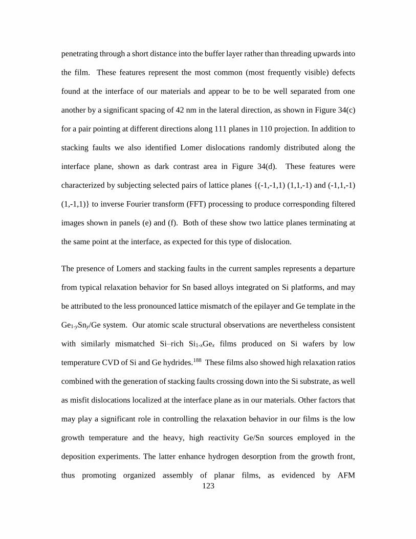
123
penetrating through a short distance into the buffer layer rather than threading upwards into
the film. These features represent the most common (most frequently visible) defects
found at the interface of our materials and appear to be to be well separated from one
another by a significant spacing of 42 nm in the lateral direction, as shown in Figure 34(c)
for a pair pointing at different directions along 111 planes in 110 projection. In addition to
stacking faults we also identified Lomer dislocations randomly distributed along the
interface plane, shown as dark contrast area in Figure 34(d). These features were
characterized by subjecting selected pairs of lattice planes {(-1,-1,1) (1,1,-1) and (-1,1,-1)
(1,-1,1)} to inverse Fourier transform (FFT) processing to produce corresponding filtered
images shown in panels (e) and (f). Both of these show two lattice planes terminating at
the same point at the interface, as expected for this type of dislocation.
The presence of Lomers and stacking faults in the current samples represents a departure
from typical relaxation behavior for Sn based alloys integrated on Si platforms, and may
be attributed to the less pronounced lattice mismatch of the epilayer and Ge template in the
Ge1-ySny/Ge system. Our atomic scale structural observations are nevertheless consistent
with similarly mismatched Si–rich Si1-xGex films produced on Si wafers by low
temperature CVD of Si and Ge hydrides.188 These films also showed high relaxation ratios
combined with the generation of stacking faults crossing down into the Si substrate, as well
as misfit dislocations localized at the interface plane as in our materials. Other factors that
may play a significant role in controlling the relaxation behavior in our films is the low
growth temperature and the heavy, high reactivity Ge/Sn sources employed in the
deposition experiments. The latter enhance hydrogen desorption from the growth front,
thus promoting organized assembly of planar films, as evidenced by AFM

124
characterizations which showed low RMS roughness in the 1-3 nm range for large areas of
20m × 20m throughout the surface. AFM also revealed cross-hatch patterns presumably
generated by dislocations penetrating to the surface or residual strain fields.
6. Quantification of Defect Density and Modeling Strain Relaxation Behavior of
Ge1-ySny/Ge Alloys
The defect formation at the interface described in the previous section has an adverse effect
on the crystalline quality of the GeSn thin films. On the other hand, relaxation of
compressive strain in the epilayers which accompanies the defect formation has a
beneficial effect on achieving direct gap behavior in GeSn alloys. The lowering of the
epilayer-substrate lattice mismatch by use of Ge/Si as a substrate rather than Si has a
significant advantage in this regard. It allows a greater degree of strain relaxation to occur
while minimizing the number of interfacial defects required for the process. The XRD
patterns of samples across the entire composition range produced in this study indicate that
the crystallinity is superior to that of similar films grown directly on Si. The FWHM of the
on axis (004) rocking curves is typically at least 3–4 times lower than observed for GeSn/Si.
For example the FWHM of ~4.5–5% Sn alloys is approximately 0.15°, which should be
compared with 0.7° for Si analogs. Furthermore, the peak profiles of the reciprocal space
maps are markedly sharper and narrower due to reduction in mosaic spread with increasing
thickness and crystallographic alignment. Moreover, the crystallinity of the samples grown
on Ge buffers is comparable across the 3–9% Sn concentration range, while in the case of
GeSn/Si the structural quality degrades significantly with increasing Sn incorporation.
In order to quantify the defect density, the samples were further characterized by
transmission electron microscopy in plan-view geometry to study the local microstructure
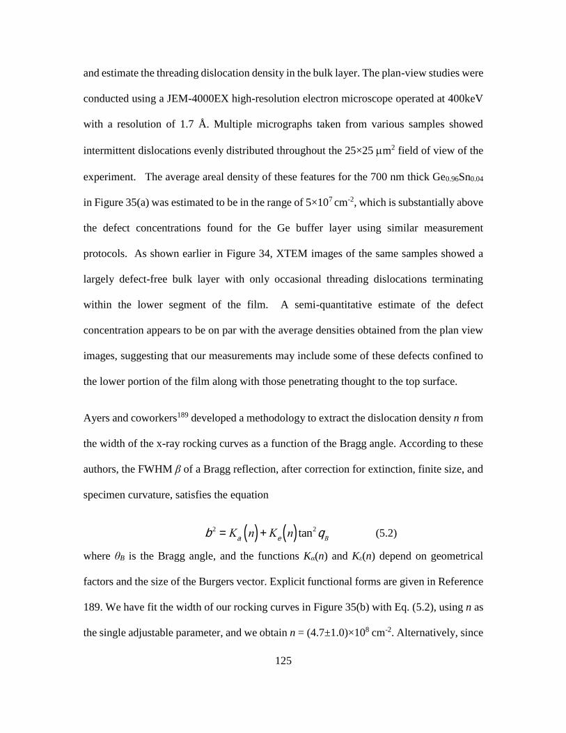
125
and estimate the threading dislocation density in the bulk layer. The plan-view studies were
conducted using a JEM-4000EX high-resolution electron microscope operated at 400keV
with a resolution of 1.7 Å. Multiple micrographs taken from various samples showed
intermittent dislocations evenly distributed throughout the 25×25 m2 field of view of the
experiment. The average areal density of these features for the 700 nm thick Ge0.96Sn0.04
in Figure 35(a) was estimated to be in the range of 5×107 cm-2, which is substantially above
the defect concentrations found for the Ge buffer layer using similar measurement
protocols. As shown earlier in Figure 34, XTEM images of the same samples showed a
largely defect-free bulk layer with only occasional threading dislocations terminating
within the lower segment of the film. A semi-quantitative estimate of the defect
concentration appears to be on par with the average densities obtained from the plan view
images, suggesting that our measurements may include some of these defects confined to
the lower portion of the film along with those penetrating thought to the top surface.
Ayers and coworkers189 developed a methodology to extract the dislocation density n from
the width of the x-ray rocking curves as a function of the Bragg angle. According to these
authors, the FWHM β of a Bragg reflection, after correction for extinction, finite size, and
specimen curvature, satisfies the equation
b 2 = K
an( )+ K
en( ) tan2q
B (5.2)
where θB is the Bragg angle, and the functions Kα(n) and Kε(n) depend on geometrical
factors and the size of the Burgers vector. Explicit functional forms are given in Reference
189. We have fit the width of our rocking curves in Figure 35(b) with Eq. (5.2), using n as
the single adjustable parameter, and we obtain n = (4.7±1.0)×108 cm-2. Alternatively, since

126
the determination of Kε(n) is affected by a large error due to the small range of Bragg angles
in our experiments, we can equate Kα(n) to the square of the width of the (111) reflection,
which has the smallest Bragg angle. Using this approach, we obtain n = 1.5×108 cm-2.
Given the fact that only order-of-magnitude estimates can be expected from the x-ray
method, as well as from the direct counting approach from the plan-view electron
micrographs, the agreement between the two methods can be considered to be satisfactory.
Next, a systematic study of the strain relaxation behavior of the Ge1-ySny/Ge/Si samples
was carried out with the hope of gaining insights that will allow the growth of fully strain
relaxed films in the direct gap composition regime. HRXRD was used to determine the
Figure 35 - (a) Plan view TEM image shows dislocations (examples marked by
arrows) with an estimated density of 5×107 cm-2. (b) Corrected FWHM of several
Bragg reflections for a Ge0.96Sn0.4 sample. The solid line is a fit with Eq. (1), in which
the dislocation density is the only adjustable parameter. The fit value is n =
(4.7±1.0)×108 cm-2.

127
strain state and relaxed cubic lattice parameters of the films, an example for which was
given earlier in Figure 27. We define the fraction of strain relaxation as R = 1-ε/εmax, where
εmax = (aGe – a0)/ a0. This fraction is shown in Figure 36, and we see that the strain in the
as-grown samples is largely relaxed. The residual compressive strain can be further reduced
or eliminated by subjecting the samples to rapid thermal annealing (RTA) treatments. For
example, the 7% Sn sample in Figure 27 possessed an as-grown strain ε= -0.10 %,
corresponding to a relaxation fraction R = 0.88. After three 2s-RTA cycles between 550oC-
600 oC, the strain was reduced down to ε= -0.05 %, which implies R =0.94, without any
indication of phase segregation or roughening of the surface. In other samples, the
relaxation after RTA exceeds 100%, indicating the appearance of tensile strain due to
thermal-expansion mismatch.
Figure 36 - Relaxation fraction R for as-grown Ge1-ySny films on Ge-buffered Si.

128
To understand the high-level of relaxation, we computed the critical thickness for growth
of GeSn/Ge using standard Mathews-Blakeslee theory.190 Starting from the effective stress
expressions proposed by Houghton,191,192 we obtain the solid black curve in Figure 37. The
elastic parameters needed for the calculation were obtained by performing Voigt
averages193,194 of the elastic constants of Ge (Ref. 154) and α-Sn (Ref. 195). From these
averages we obtain for Ge a shear modulus μ = 56.1 GPa, and a Poisson ratio ν = 0.200,
whereas for α-Sn we compute μ = 29.7 GPa, and ν = 0.217.
It is apparent from Figure 37 that all of our samples exceed the critical thickness by at least
one order of magnitude. However, since the growth temperatures are extremely low, the
possibility of significant kinetic barriers to strain relaxation cannot be ruled out. In fact,
Gencarelli et al. recently showed that fully strained Ge1-ySny/Ge samples can be fabricated
with thicknesses that far exceed the Mathews-Blakeslee prediction.76 These are shown as
black squares in Figure 37. The empty squares correspond to slightly thicker films—grown
by the same authors—that show evidence of strain relaxation. Samples grown by MBE on
Ge substrates are also found to be fully strained at thicknesses well in excess of the
Mathews-Blakeslee curve.196
A phenomenological strain relaxation model was proposed by Hull et al.197 and
systematically developed by Houghton to study Ge1-xSix alloys grown on Si.191 The model
assumes that the strain relaxation is proportional to the density of dislocation threading
segments times the dislocation velocity, while threading dislocations are created at a rate
that is proportional to an initial density n0 of incipient dislocation nuclei. A detailed account
of the model, including the effect of dislocation pinning, is given in Reference 192. We

129
have applied the same model to strain relaxation in Ge1-ySny/Ge. Houghton proposed
Arrhenius expressions for the dislocation velocity and the rate of dislocation creation, with
parameters adjusted to his own experiments in the Ge1-xSix system near the Si-rich end.191
Figure 37 - Ge1-ySny film thicknesses (empty white circles) compared with calculations
of critical thickness for strain relaxation. The solid black line is a Mathews-Blakeslee
calculation. Black squares correspond to fully strained samples reported by
Gencarelli et al. (Ref. 76), and empty squares are the thicknesses of partially relaxed
layers by the same authors. The dotted line corresponds to |εdis| =10-5 according to
Houghton’s kinetic relaxation model (Ref. 191). The parameters of the theory were
adjusted to obtain a line between Gencarelli’s fully strained and relaxed samples.
When the same parameters are used to compute the thickness at which |εdis|=10-5 for
the empty circle samples, the solid gray line is obtained. The gray area thus indicates
the region of strain “metastability”. All samples studied here are beyond this region,
which explains their high level of strain relaxation. The inset shows the annealing-
induced strain relaxation measured by Li et al. (Ref. 181)and the prediction from our
model using the same parameters as in the simulation of strain relaxation during
growth.

130
For pure Ge, detailed measurements of dislocation velocities were carried out by Yonenaga
et al. (Ref. 198), and the resulting expressions are somewhat different from those proposed
by Houghton. Since our samples are closer to pure Ge, we use the Yonenaga et al. results
in our simulations. The dislocation generation mechanism is the least known aspect of the
relaxation process, but recent results on Ge1-xSix layers on Si (Ref. 199) confirm the
importance of heterogeneous nucleation, as proposed by Houghton.191 We assume that the
expressions derived by Houghton for dislocation nucleation are valid for the Ge1-ySny
system, so that the only adjustable parameter in our model is the density n0 of incipient
dislocation nuclei. The strain relaxation produced by dislocations is defined as
εdis = εmax - ε. The fit is carried out by computing the film thickness at which this strain
relaxation reaches a value |εdis| =10-5, which is close to the limit of detectability using x-ray
methods. The dotted line in Figure 37, which gives this threshold thickness, was obtained
using n0 = 7.3×1011 cm-2 and the experimental growth rates from Gencarelli et al.(Ref.
200). Returning to our samples, we use the value of n0 obtained from the fit to the samples
in Ref. 76, combined with our growth rates and temperatures, to compute the thickness that
satisfies the |εdis| =10-5 condition. This gives the solid grey line in Figure 37. To obtain a
smooth curve, we adjusted a linear function of composition to the growth temperatures and
growth rates, which gives a good empirical account of the data for all samples in Figure
37. We see that the calculated line is well below the actual sample thicknesses, so that we
predict an observable strain relaxation level for all of our samples, as found experimentally.
In principle, the calculations can be continued beyond the solid line in Figure 37 to predict
the observed strain relaxation εdis at the actual sample thicknesses, but the values obtained
are typically lower in magnitude than those observed. This is not surprising, since the

131
model neglects dislocation multiplication, and therefore it can only be expected to be
accurate at the initial stages of strain relaxation.
The value n0 = 7.3×1011 cm-2 for the initial density of dislocation nuclei is orders of
magnitude larger than the value found by Houghton (n0 = 5×103 cm-2) for growth of Ge1-
xSix alloys on Si wafers at temperatures close to 500°C, but comparable to the values found
for Ge1-xSix films grown at temperatures near 300°C, (Ref. 192) which are much closer to
the growth temperatures of our Ge1-ySny layers. One factor that may contribute to the large
value of n0 is the use of a Ge buffer grown on Si, since the unavoidable defects in the buffer
layer may act as dislocation seeds in the Ge1-ySny layers.
To test this hypothesis we grew Ge1-ySny films directly on Ge substrates, and we find that
films with thicknesses close to 500 nm and Sn concentrations around y=0.05-0.06, well
above the metastable relaxation line in Figure 37, are still fully strained. This implies
n0 < 3×109 cm-2. A representative (224) RSM of such a fully strained sample is given in
Figure 38. It has a composition of y=0.06, and was grown at a temperature of 315°C, and
the thickness is 485 nm. The lack of strain relaxation in these films suggest that these films
should be devoid of the defects observed in the Ge1-ySny/Ge/Si films. The resultant superior
crystallinity was corroborated by examining the films using XTEM. Figure 39 a) shows a
typical cross section of the film, which has large areas of defect free crystal. In contrast to
the defected Ge1-ySny/Ge interfaces observed in the films grown on Ge buffered Si, the
interfaces of the alloys grown directly on Ge are virtually defect-free. Figure 39 b) shows
a portion of the interface which contains one of the occasional defects.

132
The lack of defects within the film is also evident when the surface of the sample is studied
using AFM. Whereas the samples grown on Ge/Si show a regular array of crosshatch
patterns on the surface, such features are absent in the films on Ge. This also results in a
smoother surface on these films with the RMS surface roughness being 0.3 nm. A
representative image is shown in Figure 40. While defect free crystals are desirable for
optical applications, the high degree of compressive strain negates this advantage by
rendering the band structure less direct gap, despite the high level of Sn incorporation.
Therefore the possibility of relaxing the films was investigated. The method chosen was
subjecting them to RTA. For the y=0.06 sample discussed earlier, it was possible to reduce
the strain to from -0.80% to -0.18% by three RTA cycles of 2 s duration at 550°C. However,
this was accompanied by a significant degradation of the crystal quality, with the FWHM
of the (004) RC increasing to 0.248° from an earlier value of 0.096°. The formation of
Figure 38 – (224) RSM of a 500 nm thick Ge0.94Sn0.06 alloy film deposited on Ge(100)
substrate. The epilayer is fully strained to the substrate, in contrast to Ge1-ySny films
deposited on Ge buffered Si substrates under similar conditions. The dashed line
emphasizes the equal in-plane lattice parameters in the substrate and epilayer.

133
threading dislocations in the film was also manifest in AFM images. As shown in Figure
40 b), crosshatch patterns generated by dislocations propagating to the surface are evident
after the annealing step. From these results, it can be concluded that using Ge as a substrate
is unsuitable for obtaining direct gap GeSn alloys, and that Ge-buffers on Si are a preferred
platform if the goal is to obtain strain-relaxed GeSn films.
7. Conclusion
GeSn films were grown on Ge-buffered Si, and their structural properties were studied in
detail. Our low temperature synthesis approach combined with the use of highly reactive
Figure 39 – a) XTEM micrograph of a Ge0.94Sn0.06 film fully strained to the Ge
substrate. b) Magnified view of the GeSn/Ge interface region exhibiting markedly
fewer defects compared to GeSn/Ge/Si samples.

134
Ge2H6/Ge3H8 and SnD4 sources provides access to material with compositions near the
direct gap threshold. Substantially lower defect levels are seen in these films compared
with films deposited directly on Si substrates, which make it possible to easily achieve
thicknesses up to 1 μm prior to the onset of epitaxy breakdown. At these thicknesses, we
find very high levels of strain relaxation, as expected from theoretical simulations of the
strain relaxation process.
In the next chapter, it will be shown how the elimination of compressive strains and the
lower defect levels leads to dramatic improvement in the intensity of optical emission. This
suggests that relaxed GeSn films on Ge-buffered Si substrates are the most promising
pathway to GeSn lasers on Si, which are the ultimate aim of this field of inquiry. The
synthetic procedures developed for fabrication of such devices is described in Chapter 7.
These methods are developed based on the procedures described in this chapter, but include
Figure 40 – a) AFM image of a 5m×5m area of an as-deposited, fully strained
Ge0.94Sn0.06/Ge film exhibiting atomically flat surface with a RMS roughness of 0.3
nm. b) The surface of the same film after strain relaxation induced by thermal
processing, exhibiting crosshatch patterns arising from propagation of dislocations to
the surface. The RMS roughness increases to 1.1 nm in this case.

135
improvements that support the deposition of thick, low defectivity alloy films with
compositions y>0.11. They include the growth of Ge refreshing layers that help mitigate
defect formation, and temperature programmed growth approaches that allow increased
growth rates at ultra-low temperatures <300°C. A detailed description of these procedures
is provided in Chapter 7, and specific details on sample growth are also given in Appendix
A.

136
CHAPTER SIX
Photoluminescence Studies of GeSn Alloys and Emission Enhancement via
n-Type Doping
Synopsis
In this chapter, PL characterization of undoped and doped GeSn alloys is described. The
intense, well resolved PL spectra from the former allowed the determination of the indirect-
direct crossover composition for the GeSn alloy system. The doped samples were mainly
synthesized using P(GeH3)3, P(SiH3)3, and As(SiH3)3 precursors at low temperatures
compatible with GeSn alloy growth near the indirect-direct crossover composition of ≈9%
Sn. The donors introduced by this method are fully activated, and carrier concentrations as
high as 7×1019 cm-3 could be achieved, resulting in an order-of magnitude and greater
enhancement in PL intensity in the doped samples compared to intrinsic counterparts.
Portions of this chapter were adapted with permission from Senaratne, C. L.; Gallagher, J.
D.; Aoki, T.; Kouvetakis, J.; Menéndez, J. Advances in light emission from group-IV
alloys via lattice engineering and n-type doping based on custom-designed chemistries.
Chem. Mater. 2014, 26 (20), 6033. Copyright 2014 American Chemical Society.
1. Introduction
Elemental Ge exhibits significant direct gap light emission in spite of the indirect character
of its fundamental band gap. This is due to the sizable population of photoexcited electrons
in the valley of the conduction band at the Brillouin zone (BZ) center, resulting from the
small energy difference between the minimum of this valley and the lowest-energy valley
in the conduction band near the L point in the Brillouin zone. As mentioned above, alloys

137
of Ge and Sn were recently introduced as a means of extending the optical capabilities of
Ge in the group IV photonics arena.9,20,51,68,69,201,202 In Ge1-ySny the separation between the
and L valleys of the Ge-like band structure is further reduced as Sn is incorporated into
the Ge lattice.36,39,41 This causes an increase in the carrier concentration in the valley,
thereby inducing more radiative transitions and thus significantly enhancing light emission
relative to pure Ge.20,38
Ge1-ySny alloys are purported to undergo an indirect to direct gap cross-over for y~ 0.06-
0.10, indicating widespread applications in future generations of light emitting devices
compatible with existing silicon technologies.36,40,41 In spite of recent advances in mapping
the electronic structure of these materials, the unambiguous determination of the cross over
composition point is very challenging.27,33–35,39,42–44,203,204 This is because it is difficult to
separate the individual contributions from two very close optical transitions if—as is the
case in GeSn —one of them (the direct gap) has an oscillator strength about two orders of
magnitude larger, and in addition the two transitions are broadened due to the alloy
potential. The only technique in which the direct and indirect gaps produce comparable
signals is room temperature photoluminescence spectroscopy, and even in this case,
measurements of the indirect gap are only possible for y ≤ 0.06. A complete and accurate
mapping of the two transitions over a broader range of compositions may require a
combination of PL with direct absorption measurements in very thick films and/or
measurements of the electrical characteristics of intrinsic and doped samples as a function
of temperature. A key requirement to accomplish this goal is the availability alloy films of
comparable quality and thickness over the entire y < 0.1 range of compositions. The

138
synthesis of such a series of films was described in the previous chapter. In this chapter,
room-temperature PL is of these alloys is measured.
The initial observation of tunable PL was obtained from sample prototypes grown directly
on Si substrates by CVD reactions Ge2H6 with SnD4.51 In this case indirect and direct gap
PL was only observed from layers with up to 3 % Sn, while the corresponding signals from
more concentrated analogs degraded significantly with increasing Sn content. This was
likely due to the increased defectivity associated with the progressively lower growth
temperatures needed to achieve higher Sn concentrations. The introduction of higher
reactivity Ge3H8 in place of Ge2H6 enabled the growth of thicker layers on silicon with Sn
contents up to 10 % Sn, spanning the direct gap composition crossover.106 These samples
were found to possess a significant volume fraction of optical quality material away for the
defective interface region, leading to sizable PL emission over the entire range of the
samples. The latter optical data were sufficient to allow an initial determination of the
compositional dependence of the direct gaps vs. Sn content. However the quality of the
PL signal was insufficient to unambiguously resolve both the direct and indirect signals
needed to determine the crossover composition and establish the nature of the fundamental
band gap. Furthermore, from a device perspective the low intensity and suboptimal quality
of the PL signal for high Sn content alloys (4-10 % Sn) indicated that the materials, as
grown on Si wafers, are not suitable for the fabrication of laser diodes.
In contrast, the GeSn alloys deposited on Ge buffered Si substrates described in the
previous chapter exhibit exceptionally strong PL signals in which it is possible to clearly
distinguish the contributions from the direct and indirect edges, as described below. This

139
stems from the fact that the virtual substrates allow the formation of thick and largely
relaxed epilayers with interface microstructures engineered to significantly reduce non-
radiative recombination velocities relative to samples grown directly on Si. Spectra from a
series of samples reveal diminishing separation between the indirect and direct band gaps,
together with dramatically increasing PL intensity with higher incorporation of Sn in the
alloys. These results, described in detail in Section 2, lead to the conclusion that the
indirect-direct crossover for the GeSn alloy system occurs in the range of 8-10 % Sn.
The PL intensity of Ge1-ySny alloys with compositions near the direct gap threshold
(y=0.05-0.09) is further enhanced by populating the -valley in the band structure with
electrons through heavy doping with P atoms at levels up to 3x10¹⁹ atoms cm-3 using the
single sources P(GeH3)3 and P(SiH3)3 whose synthesis was described in Chapter 2. In
Section 5, it is shown that show that the PL intensities of the doped films are approximately
10 times those of the intrinsic counterparts with similar thicknesses possessing the same
Sn concentration. Experiments using the As(SiH3)3 compound yielded higher carrier
densities of 7x10¹⁹/cm3 allowing additional performance gains in the PL response. The
results suggest desirable direct gap conditions for possible laser applications can be
achieved in n-type materials at relatively modest Sn contents below the direct gap
threshold.
2. Determination of Indirect-Direct Crossover in Intrinsic GeSn Alloys
PL measurements were carried out with the samples held at room temperature and
illuminated with 400 mW of radiation generated from a continuous wave (CW) 980 nm
laser focused to a 100 μm spot. The emitted light was collected by an f =140 mm Horiba

140
MicroHR spectrometer equipped with a 600 grooves/mm blazed at 2 μm. The spectrometer
is fitted with a liquid nitrogen (LN2) cooled extended InGaAs detector with a detection
range of 1300-2300 nm. A 1400 nm long pass filter is employed to remove possible
emission of visible radiation from the Si substrate. In spite of this filter, a clear 2nd order
laser signal at 1960 nm is seen in all raw spectra and is subtracted from the data by fitting
the laser peak with a Gaussian. The raw spectrum is further corrected to account for filter
transmission and spectrometer response using calibration curves obtained from
measurements of a tungsten lamp.
Figure 41 shows corrected PL spectra from selected Ge1-ySny/Ge/Si samples compared with
Ge1-ySny /Si analogs with similar Sn concentrations and thickness, collected under identical
conditions. The most striking feature in the spectra is the much stronger PL intensity from
the samples grown on Ge-buffer layers. The intensity enhancements average one order of
magnitude, and are assigned to reduced non-radiative recombination rates in the Ge1-
ySny/Ge/Si films. There are two main sources of non-radiative recombination in Ge1-ySny
films: bulk-like defects, such as threading dislocations, and defects localized at the
interface with Si, which are responsible for a very high recombination velocity at this
interface.205 Both sources of non-radiative recombination are suppressed in our Ge1-
ySny/Ge/Si films: the bulk-like defect concentration is lower, as evidenced by the reduced
widths of the XRD rocking curves, and the carriers are likely confined to the Ge1-ySny layer,
away from the Ge/Si interface, because the valence and conduction band offsets between
Ge1-ySny and Ge are of type I.206 The separation between the two contributions will require

141
systematic measurements and modeling of the PL intensity as a function of layer thickness
for a fixed Sn concentration.
Figure 41 - Photoluminescence spectra from a Ge1-ySny/Ge/Si and a Ge1-ySny/Si
counterpart with similar Sn-concentration and thickness.

142
The increased intensity of the PL signal makes it far easier to study the detailed structure
of the PL spectra, including the contributions from the direct and indirect edges. Unlike
most semiconductors, in which PL arises from the lowest band gap, whether direct or
indirect, in Ge one sees evidence for both direct and indirect gap emission.207–209 This
unique property reflects Germanium’s peculiar band structure, in which the direct band gap
is only 140 meV above the indirect edge. Even for very small thermal occupation of the
conduction band minimum associated with the direct gap, the much higher oscillator
strength of the direct optical transition leads to a signal that is comparable to the indirect
gap emission, and in fact stronger if reabsorption effects are corrected for or eliminated, as
in thin films. Figure 42 shows two examples of samples in which the direct and indirect
edge are clearly visible. As discussed in prior work,209,210 the indirect emission is fit with a
simple Gaussian and the direct gap emission is fit with an Exponentially Modified Gaussian
(EMG) function that accounts from the observed and expected asymmetry of the emission
profile. The fit with these functions is indicated as dotted (direct gap) and dash-dotted
Figure 42 - Circles and squares show photoluminescence from two selected
Ge1-ySny/Ge/Si samples. The solid line adjusted to the spectra is a fit with a
combination of a Gaussian for the indirect gap emission and an EMG for the direct
gap emissions from the Ge1-ySny top layer and the Ge buffer. The dotted and dash-
dotted lines show the three components of the fit for the two samples.

143
(indirect gap) lines in the figure. From such fits one can extract the energies of the direct
and indirect band gaps in Ge1-ySny alloys and study their compositional dependence, as
discussed below. Notice, however, that the separation between the direct and indirect
emission decreases, and the direct gap emission intensity increases, as the Sn concentration
is raised from 3% to 4.5%, approaching concentration for which the material transitions
from indirect to direct-gap semiconductor.
Figure 43 shows PL spectra from representative alloys with a common thickness of ~600
nm and varying Sn contents from 0.3 % to 9 % Sn. The PL plots for y = 0.003-0.05 show
Figure 43 - Room temperature PL plots vs. Sn fraction for Ge1-ySny (y = 0.003- 0.09).
Main peak is due to direct recombination (E0) and the weak shoulder is attributed
to indirect emission (Eind). Peak energies redshift and intensities increase as a
function of Sn content. Inset is a schematic of Ge1-ySny band structure showing the
two transitions measured in the PL spectra and the band gap narrowing in relation
to elemental Ge.

144
a strong main peak corresponding to direct gap emission and a weak lower energy shoulder
which is assigned to indirect transitions from the L minimum of the conduction band. The
two peaks appear to merge into a single broad peak in the spectra of the more concentrated
samples (y > 0.06) due to the decreasing separation of the direct and indirect edges with
increasing Sn content. The trends here illustrate a shift of the PL maximum to lower
energies as a function of Sn content and a sharp increase in the signal intensity as the
indirect-direct crossover point is approached. The direct and indirect gap energies are
extracted by fitting the PL peaks using methods described above. The same techniques
have been utilized in prior work for extracting the band gaps of (Si)GeSn analogs, as
discussed in in References 210, 211, and 212. The fitting procedure corrects for strain
effects (which are rather small due to the large strain relaxation) and yields the band gap
values corresponding to unstrained films.
The band gap energies determined using these procedures for intrinsic samples with
compositions y=0-0.11 were then fit according to quadratic expressions of the following
forms:
𝐸0(𝑦) = 𝐸0𝐺𝑒(1 − 𝑦) + 𝐸0
𝑆𝑛𝑦 − 𝑏0𝑦(1 − 𝑦) (6.1)
𝐸𝑖𝑛𝑑(𝑦) = 𝐸𝑖𝑛𝑑𝐺𝑒 (1 − 𝑦) + 𝐸𝑖𝑛𝑑
𝑆𝑛 𝑦 − 𝑏𝑖𝑛𝑑𝑦(1 − 𝑦) (6.2)
In the above expressions the E0 and Eind for y = 0 and y = 1 are taken as equal to those of
elemental Ge and α-Sn, corrected for temperature dependence. The fitting function then
contains the bowing coefficients b0 and bind as its only adjustable parameters. Using E
0
Ge
= 0.796 eV, = -0.413 eV, = 0.655 eV, and = -0.035 eV (Ref. 211), we obtain E
0
Sn
E
ind
Ge
E
ind
Sn

145
bowing parameters b0 = 2.26±0.03 eV and bind = 1.06±0.09 eV. These bowing parameters
represent a cross over point composition yc from indirect to direct gap semiconductor for
bulk like Ge1-ySny in the vicinity of 8-9%, as illustrated in Figure 44. This range is
significantly lower than predicted using virtual crystal approximation theory (yc = 0.2) but
much closer to recent calculations using supercells to simulate the alloy (4.5-6%). A more
detailed treatment of the determination of yc is given in Reference 213, which takes into
account the compositional dependence of the bowing parameters. This yields a crossover
composition of yc=0.087.
3. Growth of n-doped Ge1-ySny Alloys (y=0.04-0.09) Using P(GeH3)3 as the Doping
Agent
As noted in the introduction, the PL intensity of GeSn alloys near the indirect-direct
crossover composition can be further enhanced by n-type doping. The initial investigations
on doping was done by using P(GeH3)3 as the doping agent. The conditions used for the
growth experiments replicate the parameters used for intrinsic Ge1-ySny alloys. The growths
Figure 44 - Energies of direct gaps (circles) and indirect gaps (squares) vs. Sn
concentration for Ge1-ySny alloys with 0<y<0.11. The solid lines are the quadratic fits
of the data. The intersection near 9 % Sn denotes the onset of the crossover from
indirect to direct gap semiconductor. The gray area marks the uncertainty in cross
over composition

146
were conducted on Ge buffered Si substrates, which were cleaned before epitaxy using the
HF and Ge2H6 cleans described in Chapter 5. The growths were conducted in a hot wall
UHV-CVD reactor heated by a single zone furnace, with Ge3H8 and SnD4 as the other
precursors. The amounts of Ge3H8 used were 40-25 LTorr, with the lower amounts being
used for the higher Sn samples, for which the mixtures were diluted to 1% Ge3H8 using H2,
in contrast to the lower Sn samples, for which the concentration of Ge3H8 was 2%. The
amount of SnD4 was chosen such that the atomic percentage of Sn in the mixtures was 3-
8%, which results in the 4-9% epilayer compositions. The target doping level was ~2-
3×1019 cm-3, which was achieved by adding 0.15-0.30 LTorr of P(GeH3)3 into the precursor
mixture. The higher amounts of P(GeH3)3 were required for the samples with higher Sn
contents, presumably because of the lower growth temperatures and lower precursor
concentrations in the mixtures. The temperatures utilized for the growths were in the range
325-295°C. Specific growth parameters for representative samples are given in Appendix
A.
4. Materials Properties of P Doped GeSn Samples
Rutherford backscattering was used to determine the thickness and Sn content of the doped
samples. Channeling experiments were also carried out, the results of which demonstrate
a high degree of epitaxial alignment of the epilayers, as well as the complete
substitutionality of the Sn atoms within the Ge lattice. The RBS results are further
corroborated by high-resolution X-ray diffraction experiments. The (004) ω rocking curves
show FWHM values in the order of 0.18° for alloys in the 5-7% Sn and slightly higher for
the 8-9% materials depending on the final thickness. Such data indicate that the crystal
quality of the doped alloys is comparable to the intrinsic samples described in Chapter 5.

147
Measurement of the (224) reciprocal space maps indicated a high degree of lattice
relaxation in the as grown films in spite of the mismatch induced by increasing the Sn
content, as shown in Figure 45 a). Residual compressive strains of 0.13% corresponding
to 80% relaxation were found which can be further reduced by rapid thermal annealing.
The cubic lattice constants were obtained and the Sn contents were determined from them
using the compositional dependence relationship from Ref. 14.
The compositions derived from HRXRD data are in excellent agreement with the values
obtained from RBS analysis. The active carrier concentrations in the alloys were
determined using spectroscopic IR ellipsometry yielding values of 8×10¹⁸-3×1019 cm-3 in
all of the samples produced in this study. Nomarski optical microscopy and AFM were
used to determine the surface topology. In common with intrinsic Ge1-ySny/Ge/Si epilayers,
the doped samples exhibit cross-hatch patterns on the surface arising from the defects
generated at the interface (see Figure 45 b)). The RMS roughness as determined by AFM
was ~3-4 nm.
Further structural characterizations were performed by cross sectional transmission
electron microscopy using a JEM -4000 EX microscope operated at 400 kV. The low
magnification images revealed single phase mono-crystalline epilayers with uniform
morphologies and planar surfaces. Figure 46 shows representative micrographs of a
Ge0.936Sn0.064 film (t= 580 nm) grown upon a Ge buffer layer (t=780 nm) at 315 oC. The
STEM bright field image shows signs of defects and strain fields confined to the interface
region. The bulk film exhibits a uniform phase contrast with no threading defects visible
within the field of view of several microns in the lateral direction. This observation

148
indicates that the dislocation densities propagating through the film are relatively low and
that the misfit strain is mostly compensated at the interface. Hence we conducted a detailed
high resolution analysis to identify the type and distribution of dislocations generated under
the low temperature process conditions used in this study. The experiments were performed
on JEOL ARM 200F microscope equipped with probe aberration corrector. STEM bright
field images were acquired using large collections angles up to 22 mrad and representative
data are shown in the Figure 46 and Figure 47. The top panel in the latter illustrates an
extended view of the interface region indicating the location of stacking faults shown as
dark contrast lines along the growth direction. The features are separated from one another
by distances ranging from 42 to 15 nm as illustrated in the high resolution image in the
inset of Figure 46. These defects are randomly distributed at the GeSn/Ge interface and
they penetrate down a short distance into the buffer layers. An enlarged view of an
Figure 45 – a) 224 reciprocal space maps of a Ge0.94Sn0.06/Ge sample. The in plane
and vertical lattice parameters are determined to be 5.6984 Å and 5.7113 Å,
respectively indicating compressive strain of 0.1292%. The buffer layer exhibits a
slight tensile strain of 0.1291 % due to the thermal expansion mismatch with the Si
wafer. b) AFM image of the same film exhibits cross hatch patterns arising from
dislocation patterns near the interface penetrating through to the free surface.

149
individual stacking fault (panel (b)) shows that the disruption of the stacking sequence of
the 111 planes is caused by rotation of the dimer columns in [110] projection. This
imperfection is likely spawned by localized strain fields found in the vicinity of these
defects as a means of minimizing the residual stress induced by the lattice mismatch. In
addition to stacking faults, the STEM images also reveal 60o dislocations randomly
arranged throughout the hetero-junction. The dark contrast in panel (c) indicates the
location of such a defect which was identified by first calculating Fourier Transform of
the STEM image, and second, applying masks to only two specific {111} reflections, for
example, -1 11 and 1-1-1, filtering out everything else, and finally calculating reverse
Fourier transform of a masked FFT. The process was repeated to another set of {111}
Figure 46 - XTEM micrograph of n-type Ge0.936Sn0.064 film grown upon a Ge buffered
Si substrate at 315 oC. Inset is a high resolution STEM bright field image of the
film/buffer interface region showing the position of the interface marked by arrow
and the location of a pair of stacking faults separated by 15 nm. The doping
concentration in this sample is 3x10¹⁹/cm3 as determined by spectroscopic
ellipsometry.

150
reflections (1-11 and -11-1) and then their reverse FFT was calculated. The two reverse
FFT images are displayed in panels (d) and (e) and show that only one of them (e) contains
an extra (111) plane terminated at a point marked by the red circle indicating the presence
of a 60 degree perfect dislocation.
Finally the Ge0.936Sn0.064 sample was characterized by “element-selective” mapping using
STEM and EELS to investigate the distribution of the constituent atoms in the lattice at the
sub-nanometer scale. The atomic arrangements in these materials are of particular
relevance to the PL studies that will be described in subsequent sections, since deviations
Figure 47 - STEM images of the n-type Ge0.936Sn0.064 film grown on Ge showing defects
present in this sample. (a) Enlarged bright field view of the interface showing
stacking fault patterns commonly found in this class of materials. (b) An individual
defect is highlighted by red box illustrating rotated dimer column along {111}
direction. (c) Dark contrast in the center of the image indicates the location of the 60o
partial dislocation. (d, e) Inverse FFT images of selected {111} lattice planes in the
vicinity of the 60o dislocation is used to identify in this case the defect type denoted by
the red circle.

151
from alloy randomness may have significant implications on the electronic structure of the
crystals. The EELS spectra were collected with spot size 0.13nm in aberration corrected
STEM HAADF mode using a GATAN Enfinium spectrometer. Figure 48 (a) is a high
resolution STEM-HAADF image showing projections of atomic columns displayed as
bright spots. These correspond to dimers or dumbbells comprising Ge and Sn aligned along
the growth direction. The region of the sample analyzed by EELS is identified by the
square box with dimensions of 3x3 nm2 in the lateral direction. The thickness of the
specimen is 40 nm as determined by the low loss spectra. The EELS spectra in all cases
shows peaks corresponding to Ge (L) and Sn (M) ionization edges at 1217 eV and 483 eV,
respectively. These were then used to generate atomic maps for the Ge (green) and Sn (red)
columns as shown in Figure 48 (b) and (c) respectively. The Ge map shows distinct Ge-
Figure 48 - STEM and element selective EELS mapping show random Sn substitution
in diamond lattice. (a) STEM image of n-type Ge0.936Sn0.064 film identifying the region
analyzed by EELS; (b) Ge map created from the L edge showing dimer columns in
110 projection; (c) Sn map generated from the M edge; (d) hybrid Ge and Sn map.

152
Ge dimer rows of the host lattice. The Sn maps exhibit similar features corresponding to
projected bonding sites. The color overlay in Figure 48 (d) of the Ge and Sn maps
illustrates a uniform distribution of the green and red spots down each column indicating
that both atoms occupy the same lattice and that they are randomly located along [110]
projected columns. Collectively the XTEM and EELS analysis results support the notion
that the Ge buffers provide a structurally compatible low energy platform that serve as
compliant templates to reduce the initial lattice mismatch with Si wafers making it possible
to integrate highly concentrated alloys with large thickness, low concentrations of
threading defects and random alloy structures devoid of interstitials and precipitates as
required for meaningful investigation of the optical properties.
5. Photoluminescence Measurements and Band Gap Determination of n-type doped
films
As indicated above, heavy n-type doping of GeSn alloys by introducing group V donor
atoms leads to significant enhancement of PL emission. Figure 49 compares the spectrum
of an n-type 6 % Sn alloy containing 3x10¹⁹/cm3 carriers grown and characterized as
described in the previous sections. This sample exhibits an order of magnitude higher PL
intensity (dotted curve) relative to that of the corresponding intrinsic specimen (gray
curve), which has a similar Sn content and thickness. This increase in thickness arises from
the higher population of electrons in the valley of the doped sample, which increases the
radiative recombination probability. In addition there is a slight redshift of the doped
sample peak maximum due to the renormalization of the band gap induced by the
significant doping level.

153
Figure 50 shows PL peaks of several n-type alloys containing 4.5%, 7% and 9 % Sn and
doped with P atoms at ~ 3x1019 cm-3 active carrier concentrations. The maxima of all curves
have been normalized to facilitate comparison between films with different thicknesses.
The peaks are distinct, well-resolved and by far more intense relative to intrinsic analogs
(not shown) that were measured using the same protocols. These observations further
validate the point that n-type GeSn alloys possess enhanced emission capabilities and these
materials are uniquely suited to be employed as requisite active components for the
manufacturing of light emitters based on GeSn. The band gap energies from n-type Ge1-
ySny samples are extracted from PL spectra measured using both the InGaAs and PbS
Figure 49 - PL plots of intrinsic and phosphorus doped 6 % Sn alloy showing the
optimized the emission intensity in the doped Ge0.94Sn0.06 alloy. The intensity of
the in the n-type material is ~10 times higher than that for the as grown intrinsic
counterpart representing a significant improvement in sample performance.

154
detectors (the latter detector was employed for measuring emission in the 2300-2700 nm
spectral range) following the fitting procedure applied previously for the intrinsic analogs.
The direct and indirect gaps (circles and squares, respectively) are plotted in Figure 51 and
compared with the corresponding gaps of the intrinsic samples. The compositions of all
films described in the plots straddle the range for practical band gap engineering beyond
Ge into the mid IR from 0.8 eV down to 0.45 eV at 11 % Sn. The active carrier
concentrations are found to be in range of 0.8-3 x 10¹⁹/cm3 as indicated by the color coded
bar in the inset of the Figure 51. It is apparent from the plots that both the direct and
indirect band gap energies are lower than those of intrinsic alloys with the same Sn content.
This renormalization effect is due to the incorporation of phosphorous donor atoms in the
lattice.211 As expected there is significant noise in the indirect gap values, however in the
Figure 50 - Normalized PL spectra of n-type Ge1-ySny (n~1-3x1019 cm-3) samples with
y= 0.04, 0.07 and 0.09 recorded at room temperature using a PbS detector. The latter
enables full spectral resolution of the PL peaks at this range of Sn compositions and
P doping levels allowing an unambiguous determination of the band gap energies.
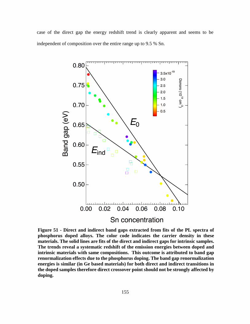
155
case of the direct gap the energy redshift trend is clearly apparent and seems to be
independent of composition over the entire range up to 9.5 % Sn.
Figure 51 - Direct and indirect band gaps extracted from fits of the PL spectra of
phosphorus doped alloys. The color code indicates the carrier density in these
materials. The solid lines are fits of the direct and indirect gaps for intrinsic samples.
The trends reveal a systematic redshift of the emission energies between doped and
intrinsic materials with same compositions. This outcome is attributed to band gap
renormalization effects due to the phosphorus doping. The band gap renormalization
energies is similar (in Ge based materials) for both direct and indirect transitions in
the doped samples therefore direct crossover point should not be strongly affected by
doping.

156
6. Group V Silyl Compounds for Doping of GeSn Alloys
In this study we expanded the single source doping strategy beyond P(GeH3)3 to examine
the use of the analogous -SiH3 precursors P(SiH3)3 and As(SiH3)3 as low-temperature high-
efficiency delivery agents of donor atoms into the group IV lattice.
6.1. Trisilylphosphine Source
The P(SiH3)3 compound is potentially a more practical CVD source than P(GeH3)3 for
scalable semiconductor processing due to its superior volatility (22 Torr vs. 2 Torr at 22
oC) and enhanced thermal stability in comparison to (PGeH3)3. With regards to the latter
we see no indication of decomposition or degradation of the molecule when it is stored
under inert conditions for several months at room temperature.
The viability of using P(SiH3)3 as a doping agent was initially investigated producing
samples in the same composition range as for the P(GeH3)3 case (i.e. y ≈ 0.04-0.08). The
growths were conducted using precursor mixtures with compositions similar to those
described earlier. These samples show maximum doping concentration of 3x10¹⁹/cm3,
indicating that the P(SiH3)3 compound does not show a decrease in efficiency as a dopant
delivery agent when compared to P(GeH3)3. Furthermore, the PL energies and emission
intensities of the corresponding samples were measured to be similar within the uncertainty
of the technique to those found in films produced via P(GeH3)3 indicating the presence of
-SiH3 or -GeH3 functionalities in the dopant compound does not significantly influence the
course of the growth process or the properties of the final product. For example samples
with composition Ge0.96Sn0.04 produced using P(GeH3)3 and P(SiH3)3 exhibited nearly
identical direct band gap energies at ~ 0.62 eV and similar PL intensities in the range of ~
1400-1600 V. The film morphology, crystal quality and final thicknesses were also

157
comparable in all films obtained using these approaches. The absolute P and Si
concentration in films grown by P(SiH3)3 were measured by SIMS using reference
standards and were found to be essentially equal at ~ 2-3 x10¹⁹. This value is consistent
with the above mentioned donor carrier densities measured by ellipsometry (3x10¹⁹/cm3)
indicating that the P atoms in the material are fully activated. The dopant profile obtained
by SIMS for P within the samples proves to be flat, in common with the samples obtained
using the germyl analog. An example of elemental profiles obtained from SIMS is given
in Figure 52. From these results, it can be concluded that the P(SiH3)3 is a viable substitute
for doping of GeSn alloys at low temperatures.
Figure 52 – Elemental profiles of Ge, P, Si and Sn obtained from a 400 nm thick
Ge0.95Sn0.05 alloy film deposited on Ge/Si(100). The absolute amounts of P and Si
obtained by comparison with an implant standard are 1.5×1019 cm-3 and
2.0×1019 cm-3 respectively. The former is within error equal to the carrier
concentration of 2.0×10¹⁹ obtained from IRSE.

158
6.2. Trisilylarsine Source
For applications such as n-channel MOSFETs, higher active carrier concentrations than
can be achieved with either P compound are required. As a potential solution for this
requirement, we were able to obtain Ge0.96Sn0.04 samples doped by As(SiH3)3 that exhibit
significantly higher active carrier densities of 7x10¹⁹ /cm3 compared to the P analogs with
similar thickness. These densities were determined by the Hall method and corroborated
using spectroscopic ellipsometry modeling of the dielectric function. The SIMS
measurements of these samples indicated that the absolute As content is fully activated
within the error of the analysis as in the case of the P(SiH3)3 doped materials above.
In the case of the As(SiH3)3 doped films the PL spectra showed significantly higher peak
intensities than those of the P(SiH3)3/P(GeH3)3 doped analogs as expected due to the two
fold increase of the free carriers. This is illustrated in Figure 53 which compares the
spectra of two representative samples with the same average Ge0.96Si0.04 composition
containing 3x10¹⁹/cm3 P and 7x10¹⁹/cm3 As donor atoms. The peak intensity of the latter
is nearly double to that of the former while the corresponding peak emission energies are
very similar. Since band filling effects push this maximum to higher energies, the result
implies a larger band gap renormalization for the n =7x10¹⁹/cm3 sample, as expected. The
ability of the As(SiH3)3 to introduce larger amounts of dopant atoms in the GeSn lattice
may be attributed to the higher reactivity of the delivery compound. Another factor may
be the larger size of the As atom which is similar to that of the bulk Ge constituents,
allowing a more facile incorporation into substitutional positions relative to the smaller P
counterpart.214 As mentioned in Chapter 4, similar behavior was observed when doping Ge
with As compared to P, where higher active carrier concentrations could be obtained using

159
the former donor. Lastly it is worth noting that the As(SiH3)3 molecule possesses
comparable volatility to P(GeH3)3 but significantly enhanced thermal stability making it
more viable for widespread CVD use. Again in this case liquid bulk samples do not
decompose when kept under inert conditions at room temperature for prolonged time
periods. These results indicate that both P(SiH3)3 and As(SiH3)3 may offer significant
advantages over P(GeH3)3 for activation of Ge based semiconductors. In this regard, it is
important to note that the co-doping with Si atoms furnished by the highly reactive -SiH3
ligands remains low for both precursors. As in the case of P descried in the previous section,
SIMS measurements were used to verify the Si contents in the As doped films, and the
concentrations are found to be close to that of the donor atom.
To account for the fact that the P/Si and As/Si ratios are nearly unity (within error) in all
doped alloys we propose that the M(SiH3)3 (M=As,P) precursors decompose under the
Figure 53 - Room temperature PL spectra of n-type Ge0.96Si0.04 grown by P(GeH3)3
and As(SiH3)3. The plots show a significant enhancement in the emission intensity with
increasing carrier concentration.

160
deposition conditions to eliminate volatile and relatively stable SiH4 or Si2H6 molecules,
which are then pumped away and therefore do not participate in the growth, and highly
reactive As-Si-H intermediates that remain adsorb on the growth surface and eventually
incorporate intact M-Si units into the films as shown by the equations below.
M(SiH3)3 Si2H6 + M-Si + 3/2H2 (6.3)
M(SiH3)3 2SiH4 + M-Si +1/2 H2 (6.4)
Due to the low level of co-doping, the basic properties of the parent lattice do not change
in any significant fashion with the incorporation of Si. This is especially important in direct
gap alloys, where incorporation of large amounts (several percent) of Si will increase the
indirect-direct crossover composition.210
For doping of Ge described in Chapter 4, Sb proved a superior donor to both P and As in
terms of achieving high carrier concentration and record low resistivities. Therefore
preliminary investigations were conducted in order to determine the possibility of using Sb
as a donor for doping GeSn in order to achieve similar advantages. It was found that
Sb(SiH3)3 source could be used as a doping agent to incorporate active Sb donors up to
levels of 5×1018 cm-3. However, when attempting to achieve higher carrier concentrations,
segregation of the Sb to the surface of the alloy film was observed in the RBS spectra of
the resultant films. While it is possible that this phenomenon can be circumvented by using
growth conditions more compatible with Sb incorporation such as lower temperatures,
from earlier investigations on doping of Ge it is evident that the SbD3 precursor provides a
more facile route for incorporating Sb into the Ge lattice. It was found that donor levels of
2×1019 cm-3 can be readily incorporated without any process optimization using the latter

161
precursor. In addition, the deposition was conducted at 273°C, and the Sn content of the
resultant epilayer was 12.5%. Therefore it can be concluded that SbD3 presents a viable
doping agent for high Sn content alloys deposited at ultra-low temperatures. Further
investigations are necessary to optimize the deposition methods involved, but based current
results the prospects for obtaining heavily Sb doped GeSn alloys with direct gap
compositions suitable for laser applications is promising.
7. Summary and Conclusions
The large thickness, low dislocation density and largely relaxed microstructure of GeSn
alloys deposited on virtual Ge substrates make them ideal candidates for band gap
determination via PL studies. This is due to the strong emission signal from such alloys
where contributions from both direct and indirect gap recombinations are present in the
same spectrum, and can be easily resolved. In the work described in this chapter, factors
leading to the enhanced emission intensity were identified, and the direct and indirect
bandgaps were measured for alloys with a wide range of compositions. This data was used
for determination of the indirect-direct crossover composition of the Ge1-ySny alloy system.
Furthermore, the work described in this chapter presents n-type doping of Ge1-ySny alloys,
which can further enhance emission intensity. The doping was carried out using both
established doping agents such as P(GeH3)3, as well as novel precursors such as M(SiH3)3
(M=P, As, Sb) and SbD3, to obtain carrier concentrations of up to 7×1019 cm-3. The heavy
n-type doping results in an order of magnitude or greater enhancement in PL intensity in
the doped samples compared to intrinsic analogs. This presents a pathway for obtaining
direct gap behavior in Ge1-ySny alloys at modest Sn contents below the indirect-direct

162
crossover composition. Indeed, stimulated emission has been observed in optically pumped
waveguides fabricated using n-type doped material described in this chapter in experiments
conducted at the University of Dayton.81 While such preliminary results are encouraging,
future work focused at identifying the optimum precursor for doping Ge1-ySny alloys at
target direct-gap compositions can be expected yield further improvement in optical
performance.
The Si containing doping agents were found to incorporate only doping levels of Si into
the GeSn alloy. This prevents the indirect-direct crossover occurring at higher Sn contents,
as has been observed for GeSiSn alloys with high silicon concentrations.210 Therefore they
represent a commercially viable option for n-type doping GeSn at low temperatures, due
to their higher thermal stability and greater volatility than previously used group V germyl
compounds.139
Finally, the excellent crystal quality of the doped alloys produced above paves the way to
their being used as platforms for further depositions. In Chapter 7, a series of pin diodes
were fabricated in which all the device components are made up of GeSn alloys. The n-
type doped bottom contact layers in these devices were fabricated using the methods
outlined above. In addition, temperature programmed growth techniques developed in
Chapter 7 for fabrication of thick (~500 nm) Ge1-ySny alloys with compositions y>0.10
were used in conjunction with the P(SiH3)3 doping agent introduced here to synthesize pn
junction diodes with direct gap compositions. These results, described in greater detail in
Chapter 7, prove the practical utility of the synthetic methods developed above.

163
CHAPTER SEVEN
Growth of GeSn Based Diode Structures and Enhancing Device Performance by
Regulation of Microstructure
Synopsis
In order to employ GeSn in optoelectronic applications, electrically injected light emission
devices must be produced. Strong PL observed from GeSn alloys deposited on Ge buffered
Si indicate that the optical properties of this platform should be suitable for developing
GeSn based LEDs. The deposition methods based on SnD4 and high order Ge hydrides was
used to produce diodes of an n-Ge/i-Ge1-ySny/p-Ge1-zSnz design which exhibit strong,
tunable EL over the wavelength range 1550 - 2700 nm and beyond. Correlation of the
microstructure of these devices with their respective EL intensities led to an optimized n-
Ge1-xSnx/i-Ge1-ySny/p-Ge1-zSnz design which exhibits enhanced emission efficiency by
eliminating interface defects. Finally, GeSn diodes with a pn junction design that acts as
the fundamental component of an electrically injected GeSn laser were fabricated, in order
to practically demonstrate the light emission capability of such devices.
Portions of this chapter were reprinted from Gallagher, J. D.; Senaratne, C. L.; Xu, C.;
Sims, P.; Aoki, T.; Smith, D. J.; Menéndez, J.; Kouvetakis, J. Non-radiative Recombination
in Ge1-ySny Light Emitting Diodes: The Role of Strain Relaxation in Tuned Heterostructure
Designs. J. Appl. Phys. 2015, 117 (24), 245704 with the permission of AIP Publishing.
Portions of this chapter have been reproduced with permission from Senaratne, C. L.;
Gallagher, J. D.; Xu, C.; Sims, P.; Menendez, J.; Kouvetakis, J. Doping of Direct Gap

164
Ge1-ySny Alloys to Attain Electroluminescence and Enhanced Photoluminescence. ECS
Trans. 2015, 69 (14), 157. Copyright 2015, The Electrochemical Society.
1. Introduction
The design and fabrication of electrically injected devices on Si platforms has attracted
considerable research attention in recent years due to potential applications in monolithic
integration of group IV photonics with Si electronics at CMOS-compatible conditions.
Recently, the lasing viability of a pseudo direct Ge-on-Si system was demonstrated.10,11 In
this case the Ge active layer was driven toward direct-gap conditions via application of
tensile strain and heavy (n > 1019 cm3) n-type doping. The main limitation of this device
type is the free-carrier absorption associated with the dopants. Furthermore, attaining high
levels of tensile strain in Ge requires high growth/annealing temperatures, which may be
incompatible with CMOS processing. An attractive alternative to overcome the limitations
of pure Ge methods is the GeSn alloy system, in which the direct-indirect band gap
difference in the material can be adjusted via compositional tuning, thus reducing and or
eliminating the need for n-type doping and tensile strain.26,215 As described in the previous
chapter, an indirect-to-direct transition occurs at ~9% Sn in the GeSn alloy system.213 This
crossover threshold is lower than early predictions, raising hopes for laser devices with
emission at wavelengths of 2400 nm and beyond.213,216 These expectations are further
supported by the recent demonstration of lasing in optically pumped GeSn devices.23
The first step to an electrically injected device using GeSn alloys is the creation of working
photodiodes. Prototype pin structures in heterostructure geometry were initially introduced
by Mathews et al. in 2009 using Ge0.98Sn0.02 active layers grown directly on p-type

165
Si(100).20 These devices were shown to exhibit enhanced responsivities, tunable
absorption edges and an extended IR coverage beyond that of Ge into the mid IR. A direct-
gap EL signal was also reported, clearly demonstrating the laser potential of this class of
materials.68 A key to the successful fabrication of such GeSn/Si devices was the substantial
progress achieved in suppressing the island-like growth of Ge-like materials on Si
substrates. However, the resulting Ge(Sn)-Si interface is still severely defected and
represents a primary concern for the operation of light-emitting devices due to its extremely
high recombination velocity approaching 1 km/s, as shown by recent studies.217
A route to achieving improved emission is via the use of a Ge buffer layer. This introduces
a separation between the active device component containing the carriers and the defected
Ge/Si interface due to the type I band alignment between Ge and GeSn. The effectiveness
of this method is clearly demonstrated in the studies described in the previous chapter,
where GeSn alloys deposited on Ge/Si substrates display an order of magnitude
enhancement in PL intensity compared to analogous material deposited directly on Si. The
same concept underlies the development of new generations of GeSn diodes exhibiting
EL.69,71,73 These devices were fabricated in pin or pn geometries grown fully-strained on
Ge or Ge-buffered Si substrates by MBE methods. The Sn concentrations of the active
regions varied between studies from 2% to 8%, while the layer thickness in all cases were
kept below 300 nm. Similar results were presented more recently based on commercially-
grown CVD samples containing 6 and 8% Sn.72 In this case the synthetic procedures were
not disclosed and pertinent film parameters including strain and microstructure were not
made available or applied to interpret the outcomes. Nevertheless, these prior studies are

166
highly encouraging and indicate that the fabrication of practical light emitting diodes with
tunable response in the mid IR is within reach.
The compressive stress in fully-strained GeSn layers on relaxed Ge buffers raises the
crossover concentration from indirect to direct gap material to yc ~ 0.2, (Ref. 211) which
is undesirable from a device perspective. On the other hand, the emission efficiency
improvement –in the form of PL– in Ge1-ySny/Ge structures relative to Ge1-ySny/Si analogs
is observed even when substantial strain relaxation has taken place at the Ge1-ySny/Ge
interface, as described in the previous chapter. This initially suggests that the defects
associated with such relaxation which are observed at the Ge1-ySny/Ge interface have a
relatively benign impact on the emission properties, so that the use of Ge buffer layers
might represent an acceptable compromise to achieve good quality emission from relaxed
GeSn layers. In contrast to the single defected interface in the above stacks, strain relaxed
GeSn devices reported in literature which employ Ge cladding layers as p- and n- type
contacts contain two defected Ge/GeSn interfaces. The increased defectivity of such a
structure may compromise the optical performance of when used for fabrication of LEDs.
In view of this, the growth of a novel n-Ge/i-Ge1-ySny/p-Ge1-zSnz (as depicted in Figure 54)
design was pursued here, in which the composition of the top p-type contact layer (z) is
tuned such that it grows pseudomorphic to the intrinsic layer, thereby creating a device
stack with only one defected interface. The growth of these diode structures, which span
the concentration range y=0.02-0.137, is described in Sections 2.1 – 2.3 of this chapter.
Given that the indirect-direct crossover composition was determined to be yc=0.087 using
PL measurements,213 these represent the first report of GeSn diodes with direct gap
compositions.

167
The microstructure of these n-Ge/i-Ge1-ySny/p-Ge1-zSnz devices (described in Section 2.5),
can be correlated to the electroluminescence efficiency, as presented in Reference 82. It
was observed that when strain relaxation defects are present at the GeSn/Ge interface, the
EL efficiency of the diodes decreases relative to devices with the same architecture but
with a non-defected GeSn/Ge interface. This analysis leads to the conclusion that even a
single defected interface has a detrimental effect on emission by increasing the non-
radiative recombination rates. A possible solution to this issue is the use of n-type doped
GeSn layers as the bottom contact. The experimental methods required for the deposition
of thick, strain relaxed, n-type GeSn alloys suitable for this purpose was described in the
previous chapter. In an n-Ge1-xSnx/i-Ge1-ySny/p-Ge1-zSnz diode structure (shown in Figure
55), tuning the bottom contact layer composition (x) to closely match the active layer
composition (y) can minimize the lattice mismatch between the two layers and prevents
strain relaxation. This additional design flexibility allows for the fabrication of fully
pseudomorphic, low strain structures even at high Sn concentrations, and can be used to
Figure 54 – Schematic of n-Ge/i-Ge1-ySny/p-Ge1-zSnz device depicting the active layer
deposited on n-doped Ge and capped by a p-type doped GeSn layer

168
carry out a detailed and systematic study of the effect of the interface defects on the
emission properties of the diodes. The growth procedures for producing devices for this
purpose are described in Section 3, together with the properties of the resultant device
stacks. It was found that the mitigation of strain relaxation between the n, i and p device
components and the resultant elimination of misfit defects substantially enhances EL
performance. Furthermore, the injection-current dependence of the electroluminescence
signal in these devices was studied, which yields the recombination lifetimes for all
structures and provides compelling evidence that eliminating strain relaxation at the device
interfaces is critical to achieving high-efficiency GeSn light-emitting diodes.
The ultimate aim of research into GeSn light emitters is the fabrication of an electrically
pumped laser diode monolithically integrated with Si. Based on the work described thus
far in this thesis, it was possible to develop deposition methods for thick, strain relaxed
GeSn films with Sn compositions above the indirect-direct crossover suitable for this
Figure 55 – Device schematic for the n-Ge1-xSnx/i-Ge1-ySny/p-Ge1-zSnz architecture

169
purpose. In addition, the doping techniques were developed that can provide degenerate n-
and p-type doping which is essential for achieving population inversion via electrical
pumping.24 A laser diode based on GeSn has several fundamental advantages. First, the
true direct gap nature of a GeSn alloy can reduce or eliminate the requirement for heavy n-
type doping, minimizing free carrier absorption seen in aforementioned Ge lasers. Second,
tensile strain is not necessary in order to obtain direct gap conditions, thereby removing
the CMOS incompatible annealing procedure from the fabrication process. As an
additional advantage GeSn alloys offer the ability to tune the wavelength into the mid-IR,
allowing access to wavelengths that cannot be reached with pure Ge. In Section 6 of this
chapter, the growth techniques developed thus far are combined to produce prototype pn
junction devices spanning the indirect-direct crossover composition regime. A schematic
of such a device is shown in Figure 56. These LEDs exhibit EL, demonstrating the emission
viability of this class of devices for the first time, and can be considered as a prelude to
fabricating an electrically injected laser using GeSn. In Reference 84 an analysis of the EL
from the various pn heterostructures described here is presented. The ability to precisely
tune the doping and composition of the device components allows the study of EL for
devices with a wide variety of parameters in the p and n device components. This work
serves to expand the fundamental understanding of factors affecting the emission
performance of quasi-direct light emitting devices.
The remainder of this chapter is organized as follows. In Section 2, the growth and
properties of diodes with the n-Ge/i-Ge1-ySny/p-Ge1-zSnz design is described. Section 3
describes the n-Ge1-xSnx/i-Ge1-ySny/p-Ge1-zSnz diode architecture, whereas Section 4
presents the study of n-Ge1-ySny/p-Ge1-zSnz diodes. Section 5 contains concluding remarks.

170
2. Device Design: n-Ge/i-Ge1-ySny/p-Ge1-zSnz Diodes
In the initial experiments, diode structures with the n-Ge/i-Ge1-ySny/p-Ge1-zSnz architecture
were produced with active layers ranging from y=0-0.137. The intrinsic GeSn alloys of the
devices were deposited on Ge buffered Si substrates. The Ge buffer layer was n-type doped,
and also used as the bottom contact of the diodes. The devices were completed by
depositing a layer of p-doped Ge1-zSnz on top of the intrinsic layer. For active layer
compositions of y<0.05, the top layer composition (z) was the approximately equal to the
active layer. For later devices with y=0.07-0.137, the devices were optimized by
maximizing carrier confinement in the active layer which increases the external quantum
efficiency. This was achieved by choosing the top layer composition to be z<y, which has
the additional advantage of minimizing the reabsorption of the light emitted from the active
area of the device.
Figure 56 – Schematic of p-Ge1-zSnz/n-Ge1-ySny LED

171
2.1. Buffer Layer Growth
The Ge buffer layers were produced by following the methods first described by Xu et al,
which were also used for the growth of Ge buffered Si substrates employed in Chapters 5
and 6.77 In brief, a mixture of Ge4H10 and P(GeH3)3 with H2 as carrier gas was used to
deposit micron thick layers of Ge on Si(100) substrates using a GSME reactor.
Commercially purchased 4-inch Si wafers were subjected to RCA cleaning prior to use as
substrates. In addition, the surface was treated with a HF/Methanol solution immediately
before loading the wafers into the growth chamber. As a final cleaning step, the wafer was
flashed at 800°C at a pressure of 10-9 Torr.
During the deposition, a 1:50 ratio of P:Ge atoms in the gaseous precursor mixture yields
films with active carrier concentrations of ~2×1019 cm-3. After deposition, which was
conducted at ~350°C under a pressure of 10-4 Torr, the Ge layers were annealed at 650°C
for three cycles each of 1 min duration. This significantly improves the crystallinity and
minimizes the threading dislocation density, thereby producing more suitable virtual
substrates on which further growth can be conducted. Therefore the final doped Ge buffer
layers, which have thicknesses of 800-1500 nm, have the same high degree of crystalline
quality as the intrinsic Ge buffer layers used for the depositions described in Chapters 5
and 6. The annealing step also introduces tensile strain in the Ge as a result of the thermal
expansion mismatch between Ge and Si. This is advantageous in that it allows alloys with
larger lattice parameters than Ge to be grown on these buffer layers, while avoiding strain
relaxation in the heterostructure design. The resultant microstructure and its effect on diode
performance will be described in detail in later sections.

172
2.2. Growth of Active Ge1-ySny Layers (y=0.02-0.137)
In the PL studies described in the previous chapters, it was found that alloy films with
thicknesses of 300 nm or greater are best suited in order to successfully obtain strong
emission with clearly resolved direct and indirect band edges. This is due to the large
volume fraction of material away from the defected interface in thicker films. The same
principle applies to electroluminescence measurements. The methods described in Chapter
5 to grow films with compositions up to y=0.11 proved a starting point for the growth of
similar thick films for the purpose of fabricating devices. Since these procedures were
described in detail earlier, only a brief description will be provided here. However, further
refinements that were necessary in order to improve the materials quality to the high
standards required to produce functional diodes will be emphasized.
For deposition of the intrinsic layers, the n-type doped virtual Ge substrates described
above were cleaved into quadrants and cleaned with HF/H2O. In addition, the surfaces were
subjected to an additional in-situ cleaning step by flowing 5% Ge2H6/H2 at a pressure of
30 mTorr prior to growth. For the device containing the y=0.02 active layer, growth was
conducted using a Ge2H6 and SnD4 precursor mixture. The deposition temperature was
335°C. When pursuing higher Sn alloys for device fabrication purposes, the use of Ge3H8
in place of Ge2H6 proved beneficial in obtaining thick films at low temperatures by
enhancing the growth rates. The y=0.05-0.07 range of compositions were achieved using
Ge3H8/SnD4 mixtures under temperatures of 315-305°C. The target Sn compositions in the
films was achieved by tuning the Ge3H8/SnD4 ratio in the precursor mixture.

173
When depositing films with higher Sn concentrations, it was found that the structural
quality of the stack could be further improved by growing a Ge ‘spacer’ layer on the wafer
surface using Ge3H8. This refreshing layer deposition was conducted at 340°C for ~25 min.
Thereafter continuous flow of Ge3H8 was maintained while the chamber cooled to the low
temperatures required for GeSn deposition. This procedure yields Ge spacers ~150 nm
thick.
The deposition of the active layer alloys with higher Sn contents was conducted at
temperatures from 295°C for y=0.085, down to 283°C for y=0.11. The precursor mixtures
were made with 22-27 LTorr of Ge3H8, and the amount of SnD4 added was varied between
5-7 LTorr. Glass containers with a volume of 3 L was used for this purpose, and the
precursors were finally diluted with of research grade H2 to a pressure of ~750 Torr to
complete the mixtures. Specific precursor amounts used for each composition are listed in
Appendix A.
At temperatures near 280°C required for the growth of alloys with compositions y>0.10,
the growth rates obtained could be further improved by following a two-stage temperature
programmed approach. This method is in contrast to the single growth temperature used
for the depositions reported thus far, and allows the growth of films with the necessary
thickness to obtain strong emission. In this new procedure, the Ge1-ySny layer deposition
was initiated at a temperature known to be conducive for the growth of Ge1-ySny layers of
the target composition. For epilayers in the y=0.11-0.137 range, this corresponds to
initiation temperatures from 280°C-270°C. Growth was allowed to proceed at this
temperature for a period of ~50 min. This procedure is expected to create a strain relaxed

174
seed layer of Ge1-ySny of the target composition, which provides a more facile template on
which further growth can proceed. The low growth temperature ensures full
substitutionality of the Sn atoms in this seed layer. Subsequently, the temperature was
slowly increased by 5°C-10°C, which increases the growth rate. The growth was then
allowed to complete at this higher temperature. A complete deposition requires ~150 min.
By following this procedure, it was possible to obtain films of Ge1-ySny in the target
composition range (y=0.12 – 0.137), whilst preventing Sn surface segregation that
accompanies Ge1-ySny growth at high temperatures. The precise temperature ranges used
are given in Appendix A, together with additional growth parameters.
In conclusion, the deposition protocols described above are capable of producing thick
(>300 nm), strain relaxed, intrinsic Ge1-ySny active layers that span the composition range
y=0.02-0.137. This broad range allows the tuning of the emission of Ge1-ySny alloys to be
tuned beyond the 1550 nm of Ge to mid-IR wavelengths of 2700 nm and beyond. Also, it
is possible to study the properties of the GeSn alloy system as an emitter material in
practical LEDs from near Ge to compositions well above the indirect-direct crossover.
These results are discussed in Section 2.7.
2.3. Growth of p-type Doped Ge1-zSnz Capping Layers
The deposition of the p-type top contact layer of the devices was carried out as a separate
deposition after growing the intrinsic layer. Before completing the top layer, the n-i stacks
resulting from the two previous steps were characterized using HRXRD and IRSE in order
to confirm that the intrinsic layer had the required thickness and composition for an active
layer of a pin diode. Prior to growth of the top contacts on the samples chosen based on

175
these criteria, the surfaces were cleaned using aqueous HF cleaning solution following a
procedure identical to that used for the Ge buffer layers in the previous stage. Thereafter
they were introduced into the growth chamber, and an additional surface clean was
performed by flowing Ge2H6 over the surface. The chamber used for the p-layer
depositions was a hot-wall CVD reactor which was heated using a three zone furnace, and
therefore had a temperature profile suitable for pre-activating the doping precursor B2H6.
The starting materials for depositing the Ge1-zSnz epilayer was provided by a Ge2H6 and
SnD4 precursor mixture. This mixture is fed into the growth chamber concomitantly with
the B2H6/H2 mixture used for doping using separate MFCs. The separation of the two
mixtures prevents reaction between the different compounds prior to entry into the growth
chamber. By adjusting the SnD4/Ge2H6 ratios and the B2H6 concentrations, p-type layers
with Sn contents z=0.02-0.10 which are doped in the 1019 cm-3 range were produced. The
temperature range used was 345°C-295°C, and the resultant epilayers have thicknesses of
80-275 nm. These properties were elucidated by studying the completed pin device stacks
via RBS, HRXRD and IRSE.
2.4. Materials Properties of n-Ge/i-Ge1-ySny/p-Ge1-zSnz Device Stacks
A representative RBS spectrum for a n-Ge/i-Ge0.863Sn0.137/p-Ge0.92Sn0.08 device stack is
given in Figure 57. The RBS random spectrum, shown in the black trace, is modelled such
that the contributions from the p, i, and n layers can be separated, giving the respective
thicknesses and Sn contents. Furthermore, channeling experiments (red trace) indicate a
high degree of crystalline alignment in the separate layers.

176
The device stacks were also subjected to HRXRD analysis. From (224) RSMs, the Sn
contents of each layer can be corroborated by calculating the relaxed lattice parameter and
determining the corresponding Sn content based on the relationship given in Reference 14.
Figure 58 shows a sample HRXRD RSM for a n-Ge/i-Ge0.87Sn0.13/p-Ge0.90Sn0.10 device
stack. The intrinsic layer exhibits a compressive strain of -0.522%, and is therefore 67%
relaxed with respect to the n-Ge buffer. This strain relaxation is enabled by the formation
of defects at the Ge1-ySny/Ge interface. A detailed account of the defect microstructure is
presented in Section 2.5. The compressive strain on the top p-contact layer, however, is
only -0.167%, which is a result of the growth of the latter on the intrinsic layer with a large
in-plane lattice constant. The pseudomorphic nature of the p-type layer growth can be seen
Figure 57 – RBS spectrum of a n-Ge/i-Ge0.863Sn0.137/p-Ge0.92Sn0.08 device.
Contributions from the three device components in the random spectrum (black
trace) can be separated based on the differences in Sn content. The Sn profiles also
indicate uniform Sn distribution within the layers. The excellent channeling (red
trace) indicates a high degree of crystalline perfection despite the high Sn content.

177
from the vertical alignment of the two peaks and the close correspondence of the in-plane
lattice parameters of the two layers (5.724 Å for the p-type layer and 5.725 Å for the
intrinsic). The relative lack of stain relaxation between the intrinsic and p-type layers is the
result of choosing the compositions such that z is close enough to y to allow lattice matched
growth. This results in a microstructure where the top i-p interface is defect free. The strain
features described above are common for all n-Ge/i-Ge1-ySny/p-Ge1-zSnz diodes fabricated
in this study.
Finally, it must be noted that the n-Ge/i-Ge0.87Sn0.13/p-Ge0.90Sn0.10 and n-Ge/i-
Ge0.863Sn0.137/p-Ge0.92Sn0.08 device stacks described in Figure 57 and Figure 58 above were
deposited using the variable temperature growth method. The uniform Sn profiles in seen
in the RBS spectra and the sharp, symmetric peaks obtained from HRXRD measurements
Figure 58 – The (224) RSM of a n-Ge/i-Ge0.87Sn0.13/p-Ge0.90Sn0.10 device structure
exhibiting the strain relaxation of the active layer relative to the Ge buffer and the
pseudomorphic growth of the top contact layer on the intrinsic layer.

178
provide evidence that this novel approach does not result in any compositional
inhomogeneity.
2.5. Microstructure of n-Ge/i-Ge1-ySny/p-Ge1-zSnz Device Stacks
As mentioned above, device structures produced using the deposition procedures described
above have active layers which span in composition from near Ge up to GeSn alloys with
direct gap Sn contents. Therefore they allow the study of the effect of increasing direct gap
behavior on EL, as will be discussed in Section 4. However, another factor which must be
considered together with the direct nature of the material when seeking to explain trends
in EL is the defect microstructure of the material, which has a direct impact on non-
radiative recombination processes. In this respect, the devices produced here have
specimens ranging from samples where n, i, and p layers are fully pseudomorphic to each
other, to samples where there is a large lattice mismatch between substrate and epilayer
resulting in strain relaxation with concomitant defect formation.
Figure 59 presents the XTEM micrograph and (224) RSM of a device of the former
category. Both intrinsic and p-type layers of the device have a composition of 2.0% Sn.
Figure 59 - (a) XTEM image of Ge/ Ge0.98Sn0.02 film. Inset contains a rare edge
dislocation marked by a white circle. Reprinted with modification from Reference 83.
(b) 224 XRD RSM for a Ge0.98Sn0.02 device showing that in this case all layers are fully
coherent. Reprinted with modification from Reference 82.

179
Due to the fact that the n-Ge virtual substrates are under tensile strain, the in plane lattice
parameter is larger than that of Ge. Therefore it is possible to grow a y=0.02 GeSn alloy
which is essentially strain relaxed and lattice matched on this substrate. By using intrinsic
and p-type doped alloys to complete a device structure of this composition, it is possible to
avoid forming interfacial defects between the different device components. The XTEM
micrograph in Figure 59 (a) was obtained from a JEOL 4000 EX microscope and illustrates
the virtually defect free interface Ge buffer layer and the GeSn alloy obtained for the above
device stack. The inset depicts a rare edge dislocation visible at the Ge/GeSn interface. The
lack of strain relaxation is corroborated by the (224) RSM given in Figure 59 (b), in which
the vertical alignment of the peaks indicate that the in-plane lattice parameters of the Ge
and GeSn layers are nearly perfectly matched. Furthermore, the proximity of the GeSn
peak to the relaxation line indicates that the epilayer is stain relaxed.
However, when the active layer contains larger amounts of Sn, the lattice mismatch
becomes greater, and strain relaxation of the epilayer ensues, as seen in the (224) RSM of
the n-Ge/i-Ge0.87Sn0.13/p-Ge0.90Sn0.10 stack given in Figure 58. The strain relaxation is
accompanied by the formation of defects at the n-Ge/i-Ge1-ySny interface. A detailed TEM
analysis of different samples was carried out in order to fully characterize the types of
defects that result from strain relaxation of the active layer. Common types of defect visible
at the interface are short stacking faults originating at the Ge1-ySny/Ge interface and
propagating into the buffer layer, and 60-degree dislocations. Figure 60 shows high
resolution STEM bright field (BF) images of defected n-Ge/i-Ge1-ySny interfaces that
exhibit both type of defects. The dark contrast areas seen in Figure 60 (a) are short stacking
faults that extend along the [111] direction and extend a short distance into the Ge buffer.

180
A similar feature seen on the left hand side of Figure 60 (b), but the defect on the right
hand side marked by a dashed circle is a 60° dislocation. These images were obtained from
n-Ge/i-Ge0.895Sn0.105 and n-Ge/i-Ge0.915Sn0.085 interfaces respectively. Another feature
observed at the n-i interface is the intersection of the stacking faults within the Ge buffer.
Such a feature is shown in Figure 61. Panel (a) of the figure shows the presence of an
intersecting pair of stacking faults together with other edge type dislocations. Panel (b) is
a close-up high resolution BF STEM micrograph of the above defect structure. The same
type of behavior was observed in GeSn alloys grown on Ge buffered Si reported in Chapter
5, and also in the growth of SiGe on Si or Ge substrates.188,218 The penetration of the defect
into the buffer rather than the active layer is beneficial for optical performance of the
device.
In contrast, the p-type top contact layer grows pseudomorphic to the active Ge1-ySny layer,
as mentioned earlier. Therefore no defect formation is observed at the i-p interface. This
5nm
Ge0.950Sn0.050
Ge0.895Sn0.105
(c)
(b)
(a)
Figure 60 – High resolution STEM BF images of defected Ge/i-Ge0.895Sn0.105 and Ge/i-
Ge0.915Sn0.085 interfaces are shown in panels (a) and (b), respectively. The images were
acquired in an aberration-corrected JEOL ARM 200F microscope. The common
defects in both cases are short stacking faults and 60o dislocations (dashed white
circle) compensating the misfit strain between the bottom contact and the intrinsic
layer of the devices. Reproduced with modification from Reference 82.

181
feature is seen in the XSTEM micrograph given in Figure 62, which was obtained from a
p-Ge0.92Sn0.08/i-Ge0.863Sn0.137/n-Ge device. The micrograph was collected using a JEOL
ARM 200F microscope. Figure 62 a) shows the entire n-i-p device stack. The top surface
is flat, and the medium angle annular dark field (MAADF) image allows the three device
components to be identified based on contrast difference dependent on Sn content and
strain differences in the constituent layers. The interfaces between the different layers are
marked by arrows. Figure 62 b) and c) are high resolution bright field (BF) images of the
top i-p interface and the bottom n-i interfaces, respectively. Typical 60° dislocations arising
due to strain relaxation can be seen at the bottom interface, while the defect free nature of
the top interface is also evident.
Figure 61 - XTEM images of the interface microstructure of a Ge0.93Sn0.07 device. (a)
Micrograph of bottom n-i interface showing edge dislocations and short stacking
faults appearing as dark contrast areas along the heterojunction. (c) Enlarged view
of two stacking faults crossing down into the Ge buffer along distinct [111] directions.
Reproduced with modification from Reference 83.

182
As mentioned earlier strain relaxation and concomitant defect generation are unavoidable
in Ge1-ySny alloys near the direct gap composition regime that have thicknesses far above
the metastable strain relaxation limits determined in Chapter 5. Indeed minimization of
compressive strain is essential to obtain direct gap behavior.211 However, the presence of
defects has a significant effect on EL performance, as described below in Section 2.7.
2.6. Device Fabrication and Diode Behavior
The pin device stacks produced using the methods outlined above were fabricated into
diodes using standard microelectronic processing procedures described in Reference 21.
The room temperature IV curves for the devices in the 0-13.7% composition regime are
plotted in Figure 63. The diodes show excellent rectifying behavior. The reverse bias dark
currents for the devices with Sn contents in the 5.5% - 8.5% regime, shown in Figure 63
(a), are comparable to devices with similar Sn contents reported in literature. However,
Figure 62 – a) XSTEM MAADF image of a p-i-n heterostructure device comprised of
an n-Ge bottom contact, i-Ge0.863Sn0.137 active layer and p-Ge0.92Sn0.08 top contact.
b) High resolution BF image of the p-GeSn/i-GeSn interface. The absence of defects
is due to pseudomorphic growth. c) High resolution BF image of defects at the
n-Ge/i-GeSn interface (marked by arrows). Reproduced with permission from
Senaratne, C. L. et al. ECS Trans. 2015, 69 (14), 157.

183
currents at forward bias for the same devices are an order of magnitude higher. This
indicates that our device fabrication procedures lead to devices with better ideality factors,
which for the 0-10.5% Sn devices shown in Figure 63 (a) range from 1.10 – 1.55. In
addition, it is also possible that our devices have lower parasitic series resistance. It was
found that by improving the device processing procedures, the dark currents which were
obtained could be lowered substantially, as shown in Figure 63 (b) for devices in the
composition range 12.0% - 13.7%. In these devices, the dark currents obtained are ~ 1
Figure 63 – IV plots of n-Ge/i-Ge1-ySny/p-Ge1-zSnz devices (a) in the 0 – 11% Sn regime,
reproduced with modification from Reference 82. (b) in the 12 – 13.7% Sn regime,
where improved device processing procedures result in an approximately order of
magnitude lowering of the dark currents.

184
A/cm2, which is an order of magnitude lower than the highest dark currents observed for
devices in the 0% – 11% range depicted in Figure 63 (a). This indicates that the materials
quality of the device stacks is not a limiting factor to obtaining further performance
improvements by employing optimized device processing procedures.
The dark currents depicted in Figure 63 (a) exhibit a compositional dependence, with
higher values being observed for samples with higher Sn contents. This behavior can be
understood by studying the temperature dependence of the dark current, as described in
Reference 82. The activation energies obtained from these measurements exceed Eg/2 for
the lower Sn samples (y<0.085), where Eg is the fundamental band gap. This indicates a
significant diffusion contribution to the dark current, as expected for devices with low
defect densities. However, for higher Sn samples (y=0.085 – 0.11), the activation energies
approach Eg/2, indicating a Shockley-Reed-Hall generation mechanism. Therefore it is
Figure 64 – Activation energies of dark currents at 0.2 V for devices with y=0-0.11,
plotted vs. Sn content and compared with the fundamental band gap and half its
value. Reproduced with modification from Reference 82.
185
evident that the higher defect densities of the higher Sn samples play a role in the dark
current increase. The activation energies for the above devices are plotted as a function of
Sn content in Figure 64.
2.7. Electroluminescence Performance of n-Ge/i-Ge1-ySny/p-Ge1-zSnz Devices
The EL of the above devices were measured at room temperature. A Keithley 2602A source
was used, and the emitted light was passed through a grating spectrometer before being
detected. For the wavelength range 1300-2300 nm, a liquid nitrogen cooled InGaAs
detector was used for this purpose. For larger wavelengths in the 1500-2700 nm range, a
thermoelectrically cooled PbS detector was necessary.
Figure 65 shows the EL spectra obtained from devices with 2.0% Sn and 7.0% Sn active
layers. The solid traces indicate the dependence of EL intensity on the injection current.
The dashed lines are the PL spectra, which in the case of Figure 65 (a) is obtained from a
single layer reference sample grown under identical conditions containing the same Sn
percentage. For of Figure 65 (b), the spectrum is from the pin device stack for which the
EL is depicted. Both PL spectra are normalized to the highest EL intensity. For the 2.0%
device, clear signals corresponding to the both direct and indirect band recombinations are
observed, whereas in the 7.0% device, the only a single peak corresponding to the direct
gap emission is seen. This is commensurate with the reduction of the separation of the
direct and indirect gaps at higher Sn concentrations elucidated from PL studies described
in the previous chapter, and indicates transition towards a direct band gap material. The
higher energy shoulder observed in the PL spectrum of the 7.0% sample is attributed to the
lower Sn p-type layer and Ge buffer that completes the device stack. The excellent

186
agreement between the PL and EL spectra indicate that the same modelling procedures
used for the former can be applied to the latter. These techniques are described in detail in
References 213 and 211, and were applied in determining the band gap values from PL
spectra as described in Chapter 6. In the above work, it was found that the line shape of the
direct gap emission can be described well by an EMG, while the indirect gap emission can
be modelled as a Gaussian function. These fits are used for comparing the EL spectra from
various devices below.
Figure 66 shows EMG fits to the direct gap from EL spectra obtained from a series of
devices with compositions y=0.0-0.12, normalized to layer thickness of the active layers.
Figure 65 – Current dependence of the EL spectra in the 0.1 – 0.5 A range for devices
with 2.0% Sn (a) and 7.0% Sn (b) active layer Sn compositions are depicted by the
solid black lines. For the 2.0% Sn device, the EL spectrum is compared with a PL
from a reference sample (dashed line) with the same Sn composition grown under the
same conditions. Good agreements between the direct and indirect gap emission from
the two experiments can be observed. For the 7.0% Sn device, the EL spectrum is
compared with the PL spectrum obtained from the entire device stack. Contributions
from the lower Sn p-GeSn layer and the Ge buffer can be seen in the latter, but good
agreement is observed in the direct gap emission from the active layer in both
experiments. The PL spectra are normalized to the EL spectra at 0.5 A in both cases.
The spectra are reproduced with modification from References 83 and 82
respectively.

187
For devices in the range y=0-0.09, the EL spectra were obtained using the LN cooled
InGaAs detector, and for the y=0.105 and y=0.12 the PbS detector was employed. The
EMG fits to the experimental data allows the comparison of intensities between the spectra
collected by different methods. The peak maxima span the range 1570-2640 nm which
demonstrates the tuning of Ge emission into the mid-IR via Sn incorporation. This series
of devices also provides the first experimental evidence that high Sn contents above the
indirect-direct crossover composition in active layers does not have a detrimental effect on
LED performance.
At room temperature, the emission intensity is expected to monotonically increase across
the composition range. Such an increase occurs as the separation between the direct and
indirect gaps is reduced with increasing Sn incorporation, resulting in greater proportion
Figure 66 – EMG fits to EL spectra obtained from a series of devices with active layers
in the composition range y=0-0.12.

188
of carrier recombinations occurring radiatively from the valley. Such an intensity
increase is observed when comparing the y=0.02 device with the Ge (y=0) device, as well
as the series of devices from y=0.055-0.12. However, the decrease in intensity between the
y=0.02 and y=0.055 devices runs contrary to this trend.
In order to explain this observation, the details of the microstructure of these devices
outlined in Section 2.5 must be considered. By limiting the defect formation to a single
interface (between the n-type and intrinsic layers), the current device design simplifies the
study of the effect of defected interfaces on optical device performance.
For both the Ge and y=0.02 devices, all three p, i and n layers are pseudomorphic. In
contrast, for the devices with y≥0.05, the intrinsic active layer is strain relaxed with respect
to the n-Ge bottom contact layer due to their large thicknesses. The resultant change in
microstructure where interfacial defect formation has taken place can be used to explain
the decrease in intensity between the y=0.02 and y=0.055 devices. The defect formation
increases the non-radiative recombination in these devices compared to the pseudomorphic
devices which lack such defects. Therefore, the EL intensity obtained from the y=0.055
device is less than that observed for the y=0.02 device, despite the active layer of the latter
being more direct in nature. The recombination lifetimes extracted from the EL spectra
given in Figure 66 are described in Reference 82, and the trend observed is a drastic
reduction of these lifetimes by approximately a factor of 2 when the n-i interface becomes
defected between the y=0.02 and y=0.055 samples. At higher Sn contents, the lifetimes
remain essentially constant, since for all devices contain defected interfaces. This allows
the decreasing separation between the direct and indirect gaps to be the dominant factor

189
determining the EL intensity. Therefore the intensities again increase in the range y=0.055-
0.12.
Based on the above results, it was identified that interfacial defect formation reduces the
emission efficiency of a device. Therefore an improved device design was developed in
which emission from relaxed alloys near the indirect-direct crossover composition could
be obtained while minimizing defect dependent non-radiative recombination. This was
achieved through Sn alloying of the buffer layer to produce devices with an n-GeSn bottom
contact, which reduces the lattice mismatch and prevents strain relaxation as described
below.
3. Eliminating Interface Defects: n-Ge1-xSnx/i-Ge1-ySny/p-Ge1-zSnz Diodes
The key to minimizing the formation of interfacial defects is reducing the lattice mismatch
between the p, i and n components of a diode. This is evident when considering the i-p
interfaces of the above devices, where due to the small difference in the lattice parameters
the p-layer growth is pseudomorphic to the i-layer. Using an n-type Ge buffer layer is no
longer a suitable option if lower lattice mismatch is to be achieved, since in the composition
range of interest strain relaxation between Ge and GeSn is unavoidable, as discussed in
Chapter 5.
A suitable alternative material that can act as an n-type contact layer and also possesses
large lattice constant is GeSn itself. As described in Chapter 6, it is possible to n-type dope
GeSn alloys to high levels using group V silyl and germyl precursors. These procedures
were now utilized in order to produce the bottom contacts of n-Ge1-xSnx/i-Ge1-ySny/p-Ge1-
zSnz device stacks.

190
The first device produced according to this design contained Sn contents of x=0.06 in the
n-layer, y=0.07 in the intrinsic layer and z=0.06 in the p-layer. The n-layer was deposited
on an intrinsic Ge virtual substrate similar to those described in Chapter 5, grown using the
methods described by Xu et al. The growth was conducted in a single zone UHV-CVD
reactor using procedures described in Chapters 5 and 6. The thickness of the layer was 410
nm, and it was doped to a level of 2.8×1019 cm-3 using P(SiH3)3. The above doping agent
was mixed together with Ge3H8 and SnD4 to make the precursor mixture for the n-layer.
After completing the growth of the n-layer, the chamber was flushed with H2 in order to
remove any residual P containing molecules which may interfere with the growth of the
intrinsic active layer. Thereafter, the Ge3H8/SnD4 mixture used for the intrinsic layer
deposition was introduced into the chamber, and the second device component was also
completed without removing the wafer from the chamber. The thickness was 550 nm.
These two layers were characterized to get the thickness and composition data from IRSE
and HRXRD. In the next step, the wafer was cleaned using aqueous HF before growing
the p-type layer, which was deposited in a 3-zone UHV-CVD reactor using Ge2H6 and
SnD4, a procedure in common with the earlier pin devices. The doping, to a level of
~3×1019 cm-3, was achieved using B2H6. All depositions were done in the 305-315°C
temperature range, and further details are given in Appendix A.
The completed device structure, a schematic of which is shown in Figure 67 (a), was
subjected to characterization using RBS, HRXRD, SIMS and IRSE techniques. This
allowed the determination of compositions, thicknesses, strains and the doping levels of
the separate layers. The peak FWHM observed in XRD RC scans and channeling RBS data
indicate excellent crystal quality of the i-Ge1-ySny layer. The Ge, Sn and P elemental

191
profiles for the device stack obtained from SIMS is shown in Figure 67 (b). The SIMS
results obtained for this structure are not only useful in establishing that full dopant
activation has occurred, but also exemplify the use of low growth temperatures in order to
obtain sharp doping transitions. Despite the intrinsic layer being grown directly after the n-
doped layer in the same chamber without an intermediate passivation step, there is no
observable P atoms in the former. This indicates that all the P precursors were removed
Figure 67 - (a) Schematic of device prototypes comprising pin layers with no strain
relaxation at the device interfaces. (b) SIMS elemental profile of a Ge0.93Sn0.07
sample showing a uniform distribution of Ge and Sn atoms across the entire
sequence of device layers as expected. The P atom content is constant through the
n region and drops sharply down to levels representative of background noise
through the intrinsic layer precluding the possibility of inter-diffusion or cross
contamination from the reactor ambient. Reprinted from Gallagher, J. D. et al. J.
Appl. Phys. 2015, 117 (24), 245704, with the permission of AIP publishing.

192
from the chamber ambient by flushing with H2 after growth of the n-type layer, eliminating
any memory effects. Furthermore, the doping profile at the interface has a sharp decrease,
which indicates that the amount of dopant diffusion which takes place is negligible. It is
possible to conclude from these results that low temperature in-situ doping techniques
which makes use of high reactivity dopant delivery agents described in this work are
capable of controlling doping to the high standards of dopant activation and precise dopant
distribution required for state of the art applications.
Despite the more complicated growth process, the advantages offered by using designs
with defect free interfaces is evident when the EL obtained from the n-Ge0.94Sn0.06/i-
Ge0.93Sn0.07/p-Ge0.94Sn0.06 device is compared with the earlier, n-Ge/i-Ge1-ySny/p-Ge1-zSnz
series of devices. In Figure 68, the EMG fits to the direct gap emission peaks from the
series of devices shown in Figure 66 are compared to the EL from the improved design. It
can be clearly seen that its intensity is higher by a factor of four or more than any of the
previous devices. This is despite the fact that the emitting layers of many of the earlier
devices contain material which have higher Sn content, and therefore greater directness,
than the y=0.07 material used in the active layer of the new design. This supports the
conclusion that strain relaxation defects, and the resultant non-radiative recombination,
have a dramatic effect on the emission efficiency of GeSn devices. The role of
recombination lifetimes in each of the different structures that quantify this observation is
discussed in detail in Reference 83. These results provide valuable guidance for optimizing
future device designs.

193
As well as providing a route to enhanced electroluminescence, lattice engineering of the
bottom n-type contact allows the synthesis of higher Sn pin diodes than can be achieved
directly on Ge. This is because a larger lattice parameter template provided by the n-GeSn
layer allows the pseudomorphic growth of the active layer, preventing the formation of
strain relaxation defects that are detrimental to the growth of high Sn diodes directly on
Ge. As an example, a 275 nm thick n-doped GeSn layer with ~11% Sn was deposited on an
n-doped Ge wafer. This deposition was designed by combining the doping techniques
developed in Chapter 6 with the variable temperature growth techniques used to obtain
Figure 68 – Comparison of EL intensity of n-Ge0.94Sn0.06/i-Ge0.93Sn0.07/p-Ge0.94Sn0.06
diode design (black line) with intensities obtained from earlier n-Ge/i-Ge1-ySny/p-Ge1-
zSnz diodes (colored lines) where y=0-0.12, as shown in Figure 66.

194
thick layers of direct gap materials described earlier in this chapter. This allows the growth
of highly n-type doped, thick, strain relaxed GeSn alloys.
After characterizing the above film to ensure its suitability as a growth platform, the device
structure was completed by depositing both i and p layers on it in a single growth. This
procedure was used to produce diode structures with active layer compositions in the
y=0.15-0.16 range. The precursor mixture used to deposit the active layer consisted of 21.3
LTorr of Ge3H8 and 10.5 LTorr of SnD4, which corresponds to a Sn/Ge ratio of 14%. The
p-type top contact was produced by flowing a 17% mixture of B2H6/H2 during final phase
of the growth. Different Sn compositions (i.e. 15% and 16%) were obtained by placing the
substrates at different positions in the growth chamber. This also resulted in a thickness
difference in the active layers, with the 15% layer being 130 nm thick and the 16% 120 nm
thick. Further experimental details on the growth of these samples can be found in
Appendix A.
Due to the reduction of the lattice mismatch and the low growth temperatures (down to
260°C) used for these growths, the active layer growth is pseudomorphic to the n-
Ge0.89Sn0.11 layer. This was verified by analyzing the device structure with XTEM, shown
in Figure 69 (a). The figure depicts the n-Ge/n-Ge0.89Sn0.11/i-Ge0.85Sn0.15/p-Ge0.85Sn0.15
device stack and the n-Ge/n-Ge0.89Sn0.11 and n-Ge0.89Sn0.11/i-Ge0.85Sn0.15 interfaces are
marked by arrows. The former interface is defected, due to the relaxation of the n-GeSn
layer relative to the Ge buffer. However, the n-Ge0.89Sn0.11/i-Ge0.85Sn0.15 interface is defect
free, indicative of pseudomorphic growth of the intrinsic layer on the n-GeSn template.
The i-Ge0.85Sn0.15/p-Ge0.85Sn0.15 interface cannot be distinguished in the micrograph,
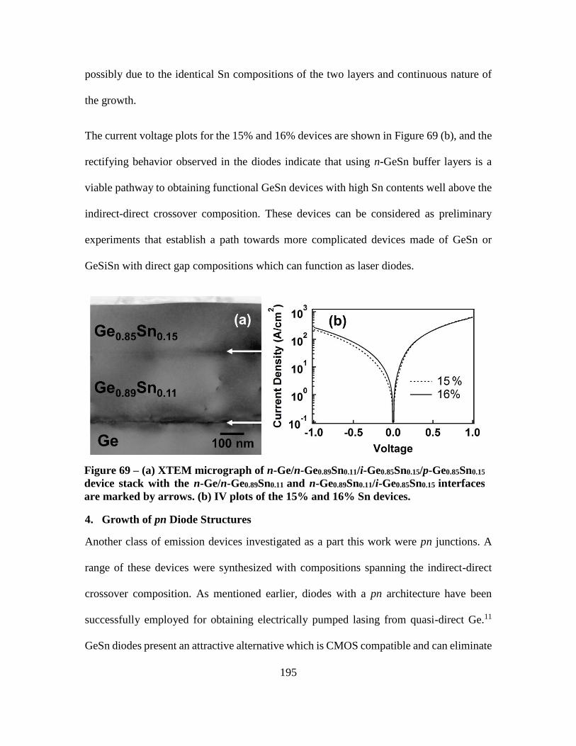
195
possibly due to the identical Sn compositions of the two layers and continuous nature of
the growth.
The current voltage plots for the 15% and 16% devices are shown in Figure 69 (b), and the
rectifying behavior observed in the diodes indicate that using n-GeSn buffer layers is a
viable pathway to obtaining functional GeSn devices with high Sn contents well above the
indirect-direct crossover composition. These devices can be considered as preliminary
experiments that establish a path towards more complicated devices made of GeSn or
GeSiSn with direct gap compositions which can function as laser diodes.
4. Growth of pn Diode Structures
Another class of emission devices investigated as a part this work were pn junctions. A
range of these devices were synthesized with compositions spanning the indirect-direct
crossover composition. As mentioned earlier, diodes with a pn architecture have been
successfully employed for obtaining electrically pumped lasing from quasi-direct Ge.11
GeSn diodes present an attractive alternative which is CMOS compatible and can eliminate
Figure 69 – (a) XTEM micrograph of n-Ge/n-Ge0.89Sn0.11/i-Ge0.85Sn0.15/p-Ge0.85Sn0.15
device stack with the n-Ge/n-Ge0.89Sn0.11 and n-Ge0.89Sn0.11/i-Ge0.85Sn0.15 interfaces
are marked by arrows. (b) IV plots of the 15% and 16% Sn devices.

196
the disadvantages of free carrier absorption and lack of wavelength tunability seen in Ge
devices.
A key factor in the successful growth of these structures were the techniques developed
earlier which allows the growth of thick, n-doped GeSn alloy films at low temperature on
Ge buffered Si substrates, which have high Sn contents that make them direct gap
semiconductors. These layers formed the bottom contact layer of the pn junctions. The
mixtures used for the n-Ge1-ySny layer growths consisted of ~27 LTorr of Ge3H8 and 4.3-
8.8 LTorr of SnD4. The resultant film compositions were y=0.065-0.123. The lower
compositions were grown at a constant temperature of 305°C, while for the high Sn content
films the initial temperature was 280°C, which was increased to 287°C during growth. The
n-type doping was achieved by adding 0.14-0.40 LTorr of P(SiH3)3 to the aforementioned
Ge3H8/SnD4 growth mixture. The ensuing active carrier concentrations were 5×1018 cm-3
– 2.5×1019 cm-3. The above reactants were combined in 3 L glass containers, and were
diluted with ~750 LTorr of H2. Specific deposition parameters for representative samples
are listed in Appendix A.
The properties of the n-type layers mentioned above were measured using HRXRD, RBS
and IRSE prior to the growth of the p-type layers which completes the device. Thereafter
the surfaces were cleaned using procedures outlined above. The top contact layers were
grown in a separate reactor using Ge2H6 and SnD4 precursors, using the same procedures
used to for the final layers of the n-Ge/i-Ge1-ySny/p-Ge1-zSnz devices. The composition
range chosen was 3.5% to 12%, and these layers were doped to levels of 1.2×1020 cm-3 –

197
1×1019 cm-3. The temperature range used for the depositions was 305°C - 285°C, and
resulted in p-type doped layers with thicknesses up to 300 nm.
An important feature of these devices in terms of obtaining efficient EL is that regardless
of whether the Sn contents of the two layers are equal or not, the growth of the top layer is
pseudomorphic to the bottom layer. This results in a defect-free p-n junction, which is
especially important in this device design, since the emission occurs from the depletion
region at the interface of the two layers. The presence of defects would result in increased
non-radiative recombination processes, degrading light emission. An example of the
microstructure is shown in the XSTEM image in Figure 70 a). The device in this case has
a n-Ge0.907Sn0.093/p-Ge0.914Sn0.086 structure where the n-type layer is 71% relaxed with
respect to the Ge buffer. The top contact layer is pseudomorphic to the latter, as seen in the
(224) RSM given in Figure 70 b).
Figure 70 – a) XSTEM BF image of n-Ge0.907Sn0.093/p-Ge0.914Sn0.086 diode structure
deposited on Ge/Si(100) substrate. The buffer-diode interface is marked by the arrow.
The top segment of the p-layer in the device is partially etched by ion milling the thin
TEM specimen. Reprinted with modification from Reference 84. b) (224) RSM of the
device structure in a).

198
Another notable feature of the interface region is the sharp transitions of the dopant profiles
at the interfaces. The elemental distribution in the different layers was obtained from SIMS,
and a representative plot for a p-Ge0.88Sn0.12/n-Ge0.88Sn0.12 device is shown in Figure 71.
The measurements were conducted using a CAMECA IMS 6f instrument, and the B profile
was obtained using an O2+ primary beam. For the heavier elements a more suitable Cs+
primary beam was used, with high mass resolution setting to prevent interference to the 31P
signal arising from the 30Si1H molecular ion. The profiles obtained from the two
measurements are combined in the figure to facilitate comparison. The absolute B and P
levels agree well with the carrier concentrations determined by ellipsometry, which are
≈2×1019 cm-3 for both layers. Most significantly, the transition from p- to n-type region is
sharp, resulting in a well-defined depletion region. Low temperature growth (≈285°C for
Figure 71 – Elemental profiles of Ge, Sn, B, P and Si obtained from SIMS for a
n-Ge0.88Sn0.12/p-Ge0.88Sn0.12 diode structure.

199
both layers) eliminate dopant diffusion which can mar the sharpness of the interfaces. The
novel dopant delivery agents discussed in Chapter 2 are the enabling factor for doping at
such conditions. Also of note is the flat and uniform Sn profile which corroborates RBS
and HRXRD results indicating homogeneous composition throughput the layers.
Properties of representative device stacks produced in this study are listed in Table 11,
which describes the Sn content, thickness and doping for p and n layers of each stack. As
can be seen from the data, the compositions and doping of the two layers was chosen in
such a way that several variants of pn junctions were produced.
In the first series of devices, the dopant level of the n-doped layer was kept low, while the
top layer was heavily doped. Furthermore, the Sn content of the top layer was chosen to be
less than that of the n-layer. In this design, the emission occurs predominantly from the
bottom layer, since the depletion region, and hence carrier recombination occurs
predominantly from the n-type layer. An example is shown in Figure 72 (a), which is
depicts the current dependent EL spectra obtained from sample A, and is reproduced with
modification from Reference 84. Due to the significant difference of Sn content between
the two device components (6.5% and 3.5% for n and p layers respectively), emission
occurring from both would result in two separate, clearly resolvable peaks. The presence
Table 11 – Thickness, composition and doping of the n and p layers of
representative n-Ge1-ySny/p-Ge1-zSnz diode stacks.
Sample Composition Thickness (nm) Doping (/cm3)
y z y z y z
A 0.064 0.033 400 100 1.3×10¹⁹ 1.2×10²⁰
B 0.123 0.077 535 100 5.6×10¹⁸ 3.0×10¹⁹
C 0.105 0.085 360 125 1.8×10¹⁹ 1.0×10¹⁹
D 0.093 0.086 525 300 4.8×10¹⁸ 2.4×10¹⁹

200
of only a single emission peak with an energy in agreement with the 6.5% Sn n-type
epilayer clearly demonstrates that the carrier recombination occurs in this region. In
addition, the current dependence of the EL intensity of the device is observed to be super-
linear, a feature in common with the pin devices described above. In sample B, the above
device design was extended to GeSn material with direct gap compositions. As shown in
Figure 72 (b), this device also exhibits clear EL arising from only the bottom n-type doped
layer, which has a composition of 12.3% Sn. Based on the composition and strain, the
emitting alloy is expected to be direct gap based on work described in Chapter 6. Peak
emission for this device is expected to be at ~2860 nm, which is beyond the cutoff point of
our detectors, and explains the observation of only the tail of the emission peak. However,
demonstration light emission from a direct gap pn junction device is an important step on
the road to an electrically injected GeSn laser.
Figure 72 – (a) Room temperature EL spectra from sample A exhibiting superlinear
current dependence. (b) Room temperature EL spectrum of sample B. Emission from
both devices occur from the n-type layer, and were collected using a LN cooled
InGaAs detector. Figure reproduced with modification from Reference 84.

201
Next, by keeping the high/low Sn contents in the bottom/top layers, but by adjusting the
doping levels to be approximately equal in both layers, it was possible to obtain two color
emission, arising from the different band gaps of the two layers. An example is sample C,
in which the n and p layer compositions are 10.5% and 8.5% Sn respectively, but doping
of both layers is comparable at 1-2×1019 cm-3. In Figure 73 (reproduced from Reference
84), the EL spectrum obtained from this sample is shown. The contributions from both p
and n layers are clearly visible, as can be expected from the more symmetric depletion
Figure 73 – Schematic and EL spectrum (grey line) of a pn diode with different Sn
contents in the two layers but with similar doping levels. The device possesses a
symmetric depletion region where carrier recombination occurs in both layers,
resulting in two color emission, fit by EMGs depicted by the dashed lines. Reprinted
with permission from Gallagher, J. D. et al. Appl. Phys. Lett. 2015, 107 (12), 123507.
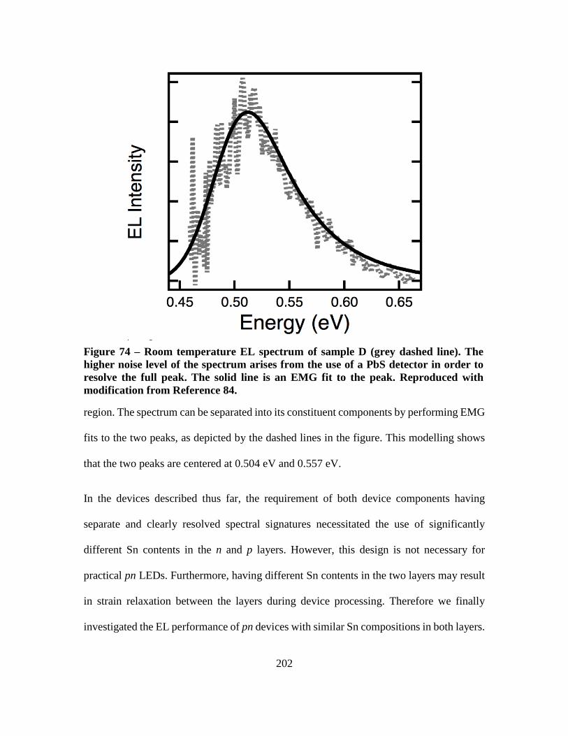
202
region. The spectrum can be separated into its constituent components by performing EMG
fits to the two peaks, as depicted by the dashed lines in the figure. This modelling shows
that the two peaks are centered at 0.504 eV and 0.557 eV.
In the devices described thus far, the requirement of both device components having
separate and clearly resolved spectral signatures necessitated the use of significantly
different Sn contents in the n and p layers. However, this design is not necessary for
practical pn LEDs. Furthermore, having different Sn contents in the two layers may result
in strain relaxation between the layers during device processing. Therefore we finally
investigated the EL performance of pn devices with similar Sn compositions in both layers.
Figure 74 – Room temperature EL spectrum of sample D (grey dashed line). The
higher noise level of the spectrum arises from the use of a PbS detector in order to
resolve the full peak. The solid line is an EMG fit to the peak. Reproduced with
modification from Reference 84.

203
An example is sample D, where the n and p layers have similar Sn contents of 9.3% and
8.6% respectively. The EL spectrum of the device is given in Figure 74, and is a single
peak centered at 0.512 eV. The emission is attributed to the n-type layer. This is due to the
fact lighter doping of the latter should result in emission predominantly confined in the n
region of the diode, similar to samples A and B described above. The results from these
EL studies are presented in greater detail in Reference 84.
The current-voltage data for samples A, B and D are given in Figure 75. The plots depict
differential current vs. applied bias, and all devices show a conductance minimum at
forward bias values of 0 - 0.2 V. Such minima are associated with Esaki-type diodes which
show negative differential resistance. In the diodes shown in Figure 75, only sample D has
a truly negative differential resistance. This may be a result of the lower strain between the
Figure 75 – Differential current vs. applied bias for samples A, B and D. Reproduced
with modification from Reference 84.

204
two components of this device, which minimizes excess currents originating from
interfacial defects.219
Overall the work described here demonstrate that GeSn pn junctions with direct gap
compositions can exhibit electrically injected light emission, and that the emission
properties of such devices can be finely tuned. Therefore these results can be considered a
strarting point for designing GeSn pn laser diodes.
5. Conclusion
In this chapter, the growth and materials characterization of GeSn diode designs were
described. The GeSn active materials of the diodes were deposited using either Ge2H6 or
Ge3H8 as the source of Ge and SnD4 as the source of Sn. The substrate chosen for the first
group of diodes was n-type doped Ge/Si(100). These provide a facile substrate for
deposition of intrinsic Ge1-ySny alloys with compositions up to y=0.14, and also act as
bottom contact layers. Therefore, by depositing p-type doped Ge1-zSnz capping layers, it is
possible to obtain diodes with an n-Ge/i-Ge1-ySny/p-Ge1-zSnz design. The diodes fabricated
in this work were the first report of electrically induced light emission from GeSn alloys
with compositions above the indirect-direct crossover point. Furthermore, the influence of
defects induced by strain relaxation at the Ge/GeSn interface on EL intensity was
investigated. This was made possible by the broad range of compositions present in the
fabricated diodes, which leads to varying degrees of strain relaxation. Based on the results
of this study, a new diode design of the n-Ge1-xSnx/i-Ge1-ySny/p-Ge1-zSnz type which
eliminates interface defects was proposed and fabricated, and was shown to have enhanced
light emission capabilities. Such designs which minimize defect densities are an essential

205
step in fabricating electrically injected GeSn lasers. Furthermore, the new design was also
found to be beneficial for further increasing the Sn content of the active layers of the diodes
(up to y=0.16) by minimizing the lattice mismatch between the layer and its immediate
substrate. Finally, diodes with a pn architecture were also fabricated. It was found that the
region of the diode contributing to light emission could be precisely controlled by adjusting
the Sn composition and doping level of the two layers. Such designs are important for
obtaining light emission from n-type doped GeSn, which has greater directness in emission
compared to intrinsic material. Therefore such devices represent viable candidates for
obtaining electrically pumped lasing from GeSn alloys at room temperature. It must be
noted that these devices are preliminary prototypes, and in future work, more complicated
architectures incorporating additional GeSn or GeSiSn components can further enhance
performance by ensuring carrier confinement in the active material while maintaining
defect-free interfaces.

206
REFERENCES
(1) Moore, G. E. Electronics 1965, 38 (8), 114.
(2) Moore, G. E. 1975 Int. Electron Devices Meet. 1975, 21, 11.
(3) Ghani, T.; Armstrong, M.; Auth, C.; Bost, M.; Charvat, P.; Glass, G.; Hoffmann, T.;
Johnson, K.; Kenyon, C.; Klaus, J.; McIntyre, B.; Mistry, K.; Murthy, A.; Sandford,
J.; Silberstein, M.; Sivakumar, S.; Smith, P.; Zawadzki, K.; Thompson, S.; Bohr, M.
In IEEE International Electron Devices Meeting 2003; IEEE, 2003; Vol. M, pp
11.6.1–11.6.3.
(4) Mistry, K.; Allen, C.; Auth, C.; Beattie, B.; Bergstrom, D.; Bost, M.; Brazier, M.;
Buehler, M.; Cappellani, A.; Chau, R.; Choi, C.-H.; Ding, G.; Fischer, K.; Ghani,
T.; Grover, R.; Han, W.; Hanken, D.; Hattendorf, M.; He, J.; Hicks, J.; Huessner,
R.; Ingerly, D.; Jain, P.; James, R.; Jong, L.; Joshi, S.; Kenyon, C.; Kuhn, K.; Lee,
K.; Liu, H.; Maiz, J.; McIntyre, B.; Moon, P.; Neirynck, J.; Pae, S.; Parker, C.;
Parsons, D.; Prasad, C.; Pipes, L.; Prince, M.; Ranade, P.; Reynolds, T.; Sandford,
J.; Shifren, L.; Sebastian, J.; Seiple, J.; Simon, D.; Sivakumar, S.; Smith, P.; Thomas,
C.; Troeger, T.; Vandervoorn, P.; Williams, S.; Zawadzki, K. In 2007 IEEE
International Electron Devices Meeting; IEEE, 2007; pp 247–250.
(5) Pillarisetty, R. Nature 2011, 479 (7373), 324.
(6) Weiner, C. IEEE Spectr. 1973, 10 (1), 24.
(7) Wolff, M. F. IEEE Spectr. 1976, 13 (8), 45.
(8) Michel, J.; Liu, J.; Kimerling, L. C. Nat. Photonics 2010, 4 (8), 527.
(9) Soref, R. Nat. Photonics 2010, 4 (8), 495.
(10) Liu, J.; Sun, X.; Camacho-Aguilera, R.; Kimerling, L. C.; Michel, J. Opt. Lett. 2010,
35 (5), 679.
(11) Camacho-aguilera, R. E.; Cai, Y.; Patel, N.; Bessette, J. T.; Romagnoli, M.;
Kimerling, L. C.; Michel, J. 2012, 20 (10), 11316.
(12) Olesinski, R. W.; Abbaschian, G. J. Bull. Alloy Phase Diagrams 1984, 5 (3), 265.
(13) Thewlis, J.; Davey, A. R. Nature 1954, 174 (4439), 1011.
(14) Beeler, R.; Roucka, R.; Chizmeshya, A. V. G.; Kouvetakis, J.; Menéndez, J. Phys.
Rev. B 2011, 84 (3), 035204.

207
(15) Takagi, S. In Advanced Gate Stacks for High-Mobility Semiconductors SE - 1;
Dimoulas, A., Gusev, E., McIntyre, P., Heyns, M., Eds.; Advanced
Microelectronics; Springer Berlin Heidelberg, 2007; Vol. 27, pp 1–19.
(16) Sau, J. D.; Cohen, M. L. Phys. Rev. B 2007, 75 (4), 045208.
(17) Liu, L.; Liang, R.; Wang, J.; Xu, J. J. Appl. Phys. 2015, 117 (18), 184501.
(18) Vincent, B.; Shimura, Y.; Takeuchi, S.; Nishimura, T.; Eneman, G.; Firrincieli, A.;
Demeulemeester, J.; Vantomme, A.; Clarysse, T.; Nakatsuka, O.; Zaima, S.;
Dekoster, J.; Caymax, M.; Loo, R. Microelectron. Eng. 2011, 88 (4), 342.
(19) Kotlyar, R.; Avci, U. E.; Cea, S.; Rios, R.; Linton, T. D.; Kuhn, K. J.; Young, I. A.
Appl. Phys. Lett. 2013, 102 (11), 113106.
(20) Mathews, J.; Roucka, R.; Xie, J.; Yu, S.-Q.; Menendez, J.; Kouvetakis, J. Appl.
Phys. Lett. 2009, 95 (13), 133506.
(21) Roucka, R.; Mathews, J.; Beeler, R. T.; Tolle, J.; Kouvetakis, J.; Menendez, J. Appl.
Phys. Lett. 2011, 98 (6), 061109.
(22) Soref, R. In Proceedings of SPIE; Kubby, J., Reed, G. T., Eds.; 2013; Vol. 8629, pp
862902–1.
(23) Wirths, S.; Geiger, R.; von den Driesch, N.; Mussler, G.; Stoica, T.; Mantl, S.;
Ikonic, Z.; Luysberg, M.; Chiussi, S.; Hartmann, J. M.; Sigg, H.; Faist, J.; Buca, D.;
Grützmacher, D. Nat. Photonics 2015, 9 (2), 88.
(24) Homewood, K. P.; Lourenço, M. A. Nat. Photonics 2015, 9 (2), 78.
(25) Farrow, R. F. C.; Robertson, D. S.; Williams, G. M.; Cullis, A. G.; Jones, G. R.;
Young, I. M.; Dennis, P. N. J. J. Cryst. Growth 1981, 54 (3), 507.
(26) Goodman, C. H. L. IEE Proc. I Solid State Electron Devices 1982, 129 (5), 189.
(27) Jenkins, D. W.; Dow, J. D. Phys. Rev. B 1987, 36 (15), 7994.
(28) Shah, S. I.; Greene, J. E.; Abels, L. L.; Yao, Q.; Raccah, P. M. J. Cryst. Growth
1987, 83 (1), 3.
(29) Asom, M. T.; Fitzgerald, E. A.; Kortan, A. R.; Spear, B.; Kimerling, L. C. Appl.
Phys. Lett. 1989, 55 (6), 578.

208
(30) Pukite, P. R.; Harwit, A.; Iyer, S. S. Appl. Phys. Lett. 1989, 54 (21), 2142.
(31) Bowman Jr., R. C.; Adams, P. M.; Engelhart, M. A.; Hochst, H. J. Vac. Sci. Technol.
A Vacuum, Surfaces, Film. 1990, 8 (3), 1577.
(32) Piao, J.; Beresford, R.; Licata, T.; Wang, W. I.; Homma, H. J. Vac. Sci. Technol. B
Microelectron. Nanom. Struct. 1990, 8 (2), 221.
(33) He, G.; Atwater, H. Phys. Rev. Lett. 1997, 79 (10), 1937.
(34) Ladron de Guevara, H. P.; Rodrıguez, A. G.; Navarro-Contreras, H.; Vidal, M. A.
Appl. Phys. Lett. 2004, 84 (22), 4532.
(35) Pérez Ladrón de Guevara, H.; Rodríguez, A. G.; Navarro-Contreras, H.; Vidal, M.
a. Appl. Phys. Lett. 2007, 91 (2007), 161909.
(36) D’Costa, V.; Cook, C.; Birdwell, A.; Littler, C.; Canonico, M.; Zollner, S.;
Kouvetakis, J.; Menéndez, J. Phys. Rev. B 2006, 73 (12), 125207.
(37) Lin, H.; Chen, R.; Lu, W.; Huo, Y.; Kamins, T. I.; Harris, J. S. Appl. Phys. Lett.
2012, 100 (10).
(38) Chen, R.; Lin, H.; Huo, Y.; Hitzman, C.; Kamins, T. I.; Harris, J. S. Appl. Phys. Lett.
2011, 99 (18), 181125.
(39) Tonkikh, A. A.; Eisenschmidt, C.; Talalaev, V. G.; Zakharov, N. D.; Schilling, J.;
Schmidt, G.; Werner, P. Appl. Phys. Lett. 2013, 103 (3), 032106.
(40) Wirths, S.; Ikonic, Z.; Tiedemann, A. T.; Hollander, B.; Stoica, T.; Mussler, G.;
Breuer, U.; Hartmann, J. M.; Benedetti, A.; Chiussi, S.; Grutzmacher, D.; Mantl, S.;
Buca, D. Appl. Phys. Lett. 2013, 103 (19), 192110.
(41) Yin, W.-J.; Gong, X.-G.; Wei, S.-H. Phys. Rev. B 2008, 78 (16), 161203.
(42) Chibane, Y.; Ferhat, M. J. Appl. Phys. 2010, 107 (5), 0.
(43) Lu Low, K.; Yang, Y.; Han, G.; Fan, W.; Yeo, Y.-C. J. Appl. Phys. 2012, 112 (10),
103715.
(44) Gupta, S.; Magyari-Kope, B.; Nishi, Y.; Saraswat, K. C. J. Appl. Phys. 2013, 113
(7), 073707.
(45) Oehme, M.; Werner, J.; Gollhofer, M.; Schmid, M.; Kaschel, M.; Kasper, E.;
Schulze, J. IEEE Photonics Technol. Lett. 2011, 23 (23), 1751.

209
(46) Shimura, Y.; Tsutsui, N.; Nakatsuka, O.; Sakai, A.; Zaima, S. Thin Solid Films 2010,
518 (6), S2.
(47) He, G.; Atwater, H. A. Nucl. Instruments Methods Phys. Res. Sect. B Beam Interact.
with Mater. Atoms 1995, 106 (1-4), 126.
(48) Tseng, H. H.; Li, H.; Mashanov, V.; Yang, Y. J.; Cheng, H. H.; Chang, G. E.; Soref,
R. A.; Sun, G. Appl. Phys. Lett. 2013, 103 (23), 231907.
(49) Taraci, J.; Tolle, J.; Kouvetakis, J.; McCartney, M. R.; Smith, D. J.; Menendez, J.;
Santana, M. A. Appl. Phys. Lett. 2001, 78 (23), 3607.
(50) Bauer, M.; Taraci, J.; Tolle, J.; Chizmeshya, A. V. G.; Zollner, S.; Smith, D. J.;
Menendez, J.; Hu, C.; Kouvetakis, J. Appl. Phys. Lett. 2002, 81 (16), 2992.
(51) Vincent, B.; Gencarelli, F.; Bender, H.; Merckling, C.; Douhard, B.; Petersen, D.
H.; Hansen, O.; Henrichsen, H. H.; Meersschaut, J.; Vandervorst, W.; Heyns, M.;
Loo, R.; Caymax, M. Appl. Phys. Lett. 2011, 99 (15), 14.
(52) Wirths, S.; Buca, D.; Mussler, G.; Tiedemann, A. T.; Holländer, B.; Bernardy, P.;
Stoica, T.; Grützmacher, D.; Mantl, S. ECS J. Solid State Sci. Technol. 2013, 2 (5),
N99.
(53) Margetis, J.; Ghetmiri, S. A.; Du, W.; Conley, B. R.; Mosleh, A.; Soref, R.; Sun, G.;
Domulevicz, L.; Naseem, H. A.; Yu, S.-Q.; Tolle, J. ECS Trans. 2014, 64 (6), 711.
(54) Suda, K.; Ishihara, S.; Sawamoto, N.; Machida, H.; Ishikawa, M.; Sudoh, H.;
Ohshita, Y.; Ogura, A. Jpn. J. Appl. Phys. 2014, 53 (11), 110301.
(55) Zaima, S.; Nakatsuka, O.; Taoka, N.; Kurosawa, M.; Takeuchi, W.; Sakashita, M.
Sci. Technol. Adv. Mater. 2015, 16 (4), 43502.
(56) Wirths, S.; Buca, D.; Mantl, S. Prog. Cryst. Growth Charact. Mater. 2016, 62 (1),
1.
(57) Taylor, M. E.; He, G.; Atwater, H. A.; Polman, A. J. Appl. Phys. 1996, 80 (8), 4384.
(58) Zheng, J.; Wang, S.; Liu, Z.; Cong, H.; Xue, C.; Li, C.; Zuo, Y.; Cheng, B.; Wang,
Q. Appl. Phys. Lett. 2016, 108 (3), 033503.
(59) Loo, R.; Vincent, B.; Gencarelli, F.; Merckling, C.; Kumar, A.; Eneman, G.; Witters,
L.; Vandervorst, W.; Caymax, M.; Heyns, M.; Thean, A. ECS J. Solid State Sci.
Technol. 2013, 2 (1), N35.

210
(60) Ike, S.; Moriyama, Y.; Kurosawa, M.; Taoka, N.; Nakatsuka, O.; Imai, Y.; Kimura,
S.; Tezuka, T.; Zaima, S. Thin Solid Films 2013, 557, 1.
(61) Gupta, S.; Chen, R.; Vincent, B.; Lin, D.; Magyari-köpe, B. ECS Trans. 2012, 50
(9), 937.
(62) Schulze, J.; Blech, A.; Datta, A.; Fischer, I. A.; Hähnel, D.; Naasz, S.; Rolseth, E.;
Tropper, E.-M. Solid. State. Electron. 2015, 110, 59.
(63) Wang, H.; Liu, Y.; Liu, M.; Zhang, Q.; Zhang, C.; Ma, X.; Zhang, J.; Hao, Y.; Han,
G. Superlattices Microstruct. 2015, 83, 401.
(64) Wirths, S.; Tiedemann, A. T.; Ikonic, Z.; Harrison, P.; Holländer, B.; Stoica, T.;
Mussler, G.; Myronov, M.; Hartmann, J. M.; Grützmacher, D.; Buca, D.; Mantl, S.
Appl. Phys. Lett. 2013, 102 (19), 10.
(65) Lei, D.; Wang, W.; Zhang, Z.; Pan, J.; Gong, X.; Liang, G.; Tok, E.; Yeo, Y.-C. J.
Appl. Phys. 2016, 119 (2), 024502.
(66) Gupta, S.; Vincent, B.; Yang, B.; Lin, D.; Gencarelli, F.; Lin, J.-Y. J.; Chen, R.;
Richard, O.; Bender, H.; Magyari-Kope, B.; Caymax, M.; Dekoster, J.; Nishi, Y.;
Saraswat, K. C. In 2012 International Electron Devices Meeting; IEEE, 2012; pp
16.2.1–16.2.4.
(67) Nishimura, T.; Nakatsuka, O.; Shimura, Y.; Takeuchi, S.; Vincent, B.; Vantomme,
A.; Dekoster, J.; Caymax, M.; Loo, R.; Zaima, S. Solid. State. Electron. 2011, 60
(1), 46.
(68) Roucka, R.; Mathews, J.; Weng, C.; Beeler, R.; Tolle, J.; Menendez, J.; Kouvetakis,
J. IEEE J. Quantum Electron. 2011, 47 (2), 213.
(69) Oehme, M.; Kasper, E.; Schulze, J. ECS J. Solid State Sci. Technol. 2013, 2 (4),
R76.
(70) Oehme, M.; Kostecki, K.; Arguirov, T.; Mussler, G.; Ye, K.; Gollhofer, M.; Schmid,
M.; Kaschel, M.; Korner, R. A.; Kittler, M.; Buca, D.; Kasper, E.; Schulze, J. IEEE
Photonics Technol. Lett. 2014, 26 (2), 187.
(71) Tseng, H. H.; Wu, K. Y.; Li, H.; Mashanov, V.; Cheng, H. H.; Sun, G.; Soref, R. A.
Appl. Phys. Lett. 2013, 102 (18), 182106.
(72) Du, W.; Zhou, Y.; Ghetmiri, S. A.; Mosleh, A.; Conley, B. R.; Nazzal, A.; Soref, R.
A.; Sun, G.; Tolle, J.; Margetis, J.; Naseem, H. A.; Yu, S.-Q. Appl. Phys. Lett. 2014,
104 (24), 241110.

211
(73) Gupta, J. P.; Bhargava, N.; Kim, S.; Adam, T.; Kolodzey, J. Appl. Phys. Lett. 2013,
102 (25), 251117.
(74) Mathews, J.; Beeler, R. T.; Tolle, J.; Xu, C.; Roucka, R.; Kouvetakis, J.; Menendez,
J. Appl. Phys. Lett. 2010, 97 (22), 221912.
(75) Grzybowski, G.; Chizmeshya, A. V. G.; Senaratne, C.; Menendez, J.; Kouvetakis,
J. J. Mater. Chem. C 2013, 1 (34), 5223.
(76) Gencarelli, F.; Vincent, B.; Demeulemeester, J.; Vantomme, A.; Moussa, A.;
Franquet, A.; Kumar, A.; Bender, H.; Meersschaut, J.; Vandervorst, W.; Loo, R.;
Caymax, M.; Temst, K.; Heyns, M. ECS J. Solid State Sci. Technol. 2013, 2 (4),
P134.
(77) Xu, C.; Beeler, R. T.; Jiang, L.; Grzybowski, G.; Chizmeshya, A. V. G.; Menéndez,
J.; Kouvetakis, J. Semicond. Sci. Technol. 2013, 28 (10), 105001.
(78) Cook, C. S. Growth and optical properties of novel doped and undoped group IV
materials based on silicon, germanium, and tin, Arizona State University, 2006.
(79) Bauer, M. R. Synthesis of new tin-germanium-silicon semiconductors with tunable
direct band gaps, Arizona State University, 2003.
(80) Chizmeshya, A. V. G.; Ritter, C.; Tolle, J.; Cook, C.; Menéndez, J.; Kouvetakis, J.
Chem. Mater. 2006, 18 (26), 6266.
(81) Li, Z. Room Temperature Lasing in GeSn Alloys, University of Dayton, 2015.
(82) Gallagher, J. D.; Senaratne, C. L.; Sims, P.; Aoki, T.; Menéndez, J.; Kouvetakis, J.
Appl. Phys. Lett. 2015, 106 (9), 091103.
(83) Gallagher, J. D.; Senaratne, C. L.; Xu, C.; Sims, P.; Aoki, T.; Smith, D. J.;
Menéndez, J.; Kouvetakis, J. J. Appl. Phys. 2015, 117 (24), 245704.
(84) Gallagher, J. D.; Senaratne, C. L.; Wallace, P. M.; Menéndez, J.; Kouvetakis, J.
Appl. Phys. Lett. 2015, 107 (12), 123507.
(85) Al-Kabi, S.; Ghetmiri, S. A.; Margetis, J.; Du, W.; Mosleh, A.; Alher, M.; Dou, W.;
Grant, J. M.; Sun, G.; Soref, R. A.; Tolle, J.; Li, B.; Mortazavi, M.; Naseem, H. A.;
Yu, S.-Q. J. Electron. Mater. 2015, 1.
(86) Stange, D.; Wirths, S.; von den Driesch, N.; Mussler, G.; Stoica, T.; Ikonic, Z.;
Hartmann, J. M.; Mantl, S.; Grützmacher, D.; Buca, D. ACS Photonics 2015, 2 (11),
1539.

212
(87) Yu, S. Q.; Ghetmiri, S. A.; Du, W.; Margetis, J.; Zhou, Y.; Mosleh, A.; Al-Kabi, S.;
Nazzal, A.; Sun, G.; Soref, R. A.; Tolle, J.; Li, B.; Naseem, H. A. In Proc. SPIE
9367, Silicon Photonics X; Reed, G. T., Watts, M. R., Eds.; 2015; Vol. 9367, p
93670R.
(88) Pham, T.; Du, W.; Tran, H.; Margetis, J.; Tolle, J.; Sun, G.; Soref, R. A.; Naseem,
H. A.; Li, B.; Yu, S.-Q. Opt. Express 2016, 24 (5), 4519.
(89) Stange, D.; von den Driesch, N.; Rainko, D.; Schulte-Braucks, C.; Wirths, S.;
Mussler, G.; Tiedemann, A. T.; Stoica, T.; Hartmann, J. M.; Ikonic, Z.; Mantl, S.;
Grützmacher, D.; Buca, D. Opt. Express 2016, 24 (2), 1358.
(90) Schulte-Braucks, C.; Stange, D.; von den Driesch, N.; Blaeser, S.; Ikonic, Z.;
Hartmann, J. M.; Mantl, S.; Buca, D. Appl. Phys. Lett. 2015, 107 (4), 042101.
(91) Grzybowski, G.; Jiang, L.; Beeler, R. T.; Watkins, T.; Chizmeshya, A. V. G.; Xu,
C.; Menéndez, J.; Kouvetakis, J. Chem. Mater. 2012, 24 (9), 1619.
(92) Norman, A. D.; Webster, J. R.; Jolly, W. L.; Gorse, R. A.; Bornhorst, W. R.; Ring,
M. A. Inorg. Synth. 1968, 11, 170.
(93) D’Costa, V. R.; Fang, Y.; Mathews, J.; Roucka, R.; Tolle, J.; Menéndez, J.;
Kouvetakis, J. Semicond. Sci. Technol. 2009, 24 (11), 115006.
(94) Grzybowski, G.; Beeler, R. T.; Jiang, L.; Smith, D. J.; Kouvetakis, J.; Menéndez, J.
Appl. Phys. Lett. 2012, 101 (7), 072105.
(95) Finholt, A. E.; Bond, A. C.; Schlesinger, H. I. J. Am. Chem. Soc. 1947, 69 (5), 1199.
(96) Grzybowski, G. Epitaxy of group IV optical materials and synthesis of IV/III-V
semiconductor analogs by designer hydride chemistries., Arizona State University,
Tempe, AZ, 2013.
(97) Todd, M. A.; Bandari, G.; Baum, T. H. Chem. Mater. 1999, 11 (3), 547.
(98) Drake, J. E.; Glavincevski, B. M.; Hemmings, R. T.; Henderson, H. E.; Ebsworth,
E. A. V; Henderson, S. G. D. Inorg. Synth. 1979, 19, 274.
(99) Goldfarb, T. D.; Sujishi, S. J. Am. Chem. Soc. 1964, 86 (9), 1679.
(100) Bentham, J. E.; Cradock, S.; Ebsworth, E. A. V. Inorg. Nucl. Chem. Lett. 1971, 7
(11), 1077.
(101) Norman, A. D.; Jolly, W. L.; Saturnino, D.; Shore, S. G. Inorg. Synth. 1968, 11, 15.

213
(102) Luryi, S.; Kastalsky, A.; Bean, J. C. IEEE Trans. Electron Devices 1984, 31 (9),
1135.
(103) Baribeau, J. M.; Jackman, T. E.; Houghton, D. C.; Maigné, P.; Denhoff, M. W. J.
Appl. Phys. 1988, 63 (100), 5738.
(104) Colace, L.; Masini, G.; Galluzzi, F.; Assanto, G.; Capellini, G.; Di Gaspare, L.;
Palange, E.; Evangelisti, F. Appl. Phys. Lett. 1998, 72 (24), 3175.
(105) Luan, H.-C.; Lim, D. R.; Lee, K. K.; Chen, K. M.; Sandland, J. G.; Wada, K.;
Kimerling, L. C. Appl. Phys. Lett. 1999, 75, 2909.
(106) Grzybowski, G.; Beeler, R. T.; Jiang, L.; Smith, D. J.; Kouvetakis, J.; Menéndez, J.
Appl. Phys. Lett. 2012, 101 (100), 0.
(107) Xu, C.; Beeler, R. T.; Grzybowski, G. J.; Chizmeshya, A. V. G.; Smith, D. J.;
Menéndez, J.; Kouvetakis, J. J. Am. Chem. Soc. 2012, 134 (51), 20756.
(108) Shimoda, T.; Matsuki, Y.; Furusawa, M.; Aoki, T.; Yudasaka, I.; Tanaka, H.;
Iwasawa, H.; Wang, D.; Miyasaka, M.; Takeuchi, Y. Nature 2006, 440 (7085), 783.
(109) Han, S.; Dai, X.; Loy, P.; Lovaasen, J.; Huether, J.; Hoey, J. M.; Wagner, A.;
Sandstrom, J.; Bunzow, D.; Swenson, O. F.; Akhatov, I. S.; Schulz, D. L. J. Non.
Cryst. Solids 2008, 354 (19-25), 2623.
(110) Kim, S.; Han, T.-H.; Jung, H.; Oh, Y.-S.; Pu, L.; Lee, P.-C.; Nam, J.-D. J. Mater.
Chem. 2011, 21 (9), 3025.
(111) Frisch, M. J.; Trucks, G. W.; Schlegel, H. B.; Scuseria, G. E.; Robb, M. A.;
Cheeseman, J. R.; Montgomery Jr., J. A.; Vreven, T.; Kudin, K. N.; Burant, J. C.;
Millam, J. M.; Iyengar, S. S.; Tomasi, J.; Barone, V.; Mennucci, B.; Cossi, M.;
Scalmani, G.; Rega, N.; Petersson, G. A.; Nakatsuji, H.; Hada, M.; Ehara, M.;
Toyota, K.; Fukuda, R.; Hasegawa, J.; Ishida, M.; Nakajima, T.; Honda, Y.; Kitao,
O.; Nakai, H.; Klene, M.; Li, X.; Knox, J. E.; Hratchian, H. P.; Cross, J. B.; Bakken,
V.; Adamo, C.; Jaramillo, J.; Gomperts, R.; Stratmann, R. E.; Yazyev, O.; Austin,
A. J.; Cammi, R.; Pomelli, C.; Ochterski, J. W.; Ayala, P. Y.; Morokuma, K.; Voth,
G. A.; Salvador, P.; Dannenberg, J. J.; Zakrzewski, V. G.; Dapprich, S.; Daniels, A.
D.; Strain, M. C.; Farkas, O.; Malick, D. K.; Rabuck, A. D.; Raghavachari, K.;
Foresman, J. B.; Ortiz, J. V.; Cui, Q.; Baboul, A. G.; Clifford, S.; Cioslowski, J.;
Stefanov, B. B.; Liu, G.; Liashenko, A.; Piskorz, I.; Komaromi, P.; Martin, R. L.;
Fox, D. J.; Keith, T.; Al-Laham, M. A.; Peng, C. Y.; Nanayakkara, A.; Challacombe,
M.; Gill, P. M. W.; Johnson, B.; Chen, W.; Wong, M. W.; Gonzalez, C.; Pople, J.
A. Gaussian03, Revision C.; Gaussian, Inc.: Wellingford, CT, 2004.
(112) Pitzer, K. S.; Gwinn, W. D. J. Chem. Phys. 1942, 10 (7), 428.

214
(113) Mackay, K. M.; Sutton, K. J. J. Chem. Soc. A Inorganic, Phys. Theor. 1968, No.
2312, 2312.
(114) Wistey, M. A.; Fang, Y.-Y.; Tolle, J.; Chizmeshya, A. V. G.; Kouvetakis, J. Appl.
Phys. Lett. 2007, 90 (8), 082108.
(115) Xu, C.; Gallagher, J. D.; Sims, P.; Smith, D. J.; Menéndez, J.; Kouvetakis, J.
Semicond. Sci. Technol. 2015, 30 (4), 045007.
(116) Spitzer, W. G.; Trumbore, F. A.; Logan, R. A. J. Appl. Phys. 1961, 32 (10), 1822.
(117) Xu, C.; Gallagher, J. D.; Wallace, P. M.; Senaratne, C. L.; Sims, P.; Menéndez, J.;
Kouvetakis, J. Semicond. Sci. Technol. 2015, 30 (10), 105028.
(118) Kouvetakis, J.; Favaro, R.; Grzybowski, G. J.; Senaratne, C.; Menéndez, J.;
Chizmeshya, A. V. G. Chem. Mater. 2014, 26 (15), 4447.
(119) Claeys, C.; Simoen, E. Germanium-based technologies: from materials to devices;
Elsevier, 2011.
(120) Vanhellemont, J.; Simoen, E. Mater. Sci. Semicond. Process. 2012, 15 (6), 642.
(121) Chui, C. O.; Kulig, L.; Moran, J.; Tsai, W.; Saraswat, K. C. Appl. Phys. Lett. 2005,
87 (9), 091909.
(122) Simoen, E.; Satta, A.; D’Amore, A.; Janssens, T.; Clarysse, T.; Martens, K.; De
Jaeger, B.; Benedetti, A.; Hoflijk, I.; Brijs, B.; Meuris, M.; Vandervorst, W. Mater.
Sci. Semicond. Process. 2006, 9 (4-5 SPEC. ISS.), 634.
(123) Tsouroutas, P.; Tsoukalas, D.; Zergioti, I.; Cherkashin, N.; Claverie, A. Mater. Sci.
Semicond. Process. 2008, 11 (5), 372.
(124) Dilliway, G.; Van Den Boom, R.; Van Daele, B.; Leys, F. E.; Clarysse, T.;
Parmentier, B.; Moussa, A.; Defranoux, C.; Benedetti, A.; Richard, O.; Bender, H.;
Simoen, E.; Meuris, M. M. ECS Trans. 2006, 3 (7), 599.
(125) Yamamoto, Y.; Kurps, R.; Mai, C.; Costina, I.; Murota, J.; Tillack, B. Solid. State.
Electron. 2013, 83, 25.
(126) Yu, H.-Y.; Battal, E.; Okyay, A. K.; Shim, J.; Park, J.-H.; Baek, J. W.; Saraswat, K.
C. Curr. Appl. Phys. 2013, 13 (6), 1060.
(127) Poon, C. H.; Tan, L. S.; Cho, B. J.; Du, A. Y. J. Electrochem. Soc. 2005, 152 (12),
G895.

215
(128) Moriyama, Y.; Kamimuta, Y.; Kamata, Y.; Ikeda, K.; Sakai, A.; Tezuka, T. Appl.
Phys. Express 2014, 7 (10), 106501.
(129) Satta, A.; Simoen, E.; Duffy, R.; Janssens, T.; Clarysse, T.; Benedetti, A.; Meuris,
M.; Vandervorst, W. Appl. Phys. Lett. 2006, 88 (16), 5.
(130) Jang, S.-M.; Liao, K.; Reif, R. J. Electrochem. Soc. 1995, 142 (10), 3520.
(131) Tutuc, E.; Chu, J. O.; Ott, J. A.; Guha, S. Appl. Phys. Lett. 2006, 89 (26), 7.
(132) Hartmann, J. M.; Barnes, J. P.; Veillerot, M.; Fédéli, J. M.; Benoit A La Guillaume,
Q.; Calvo, V. J. Cryst. Growth 2012, 347 (1), 37.
(133) Scappucci, G.; Capellini, G.; Klesse, W. M.; Simmons, M. Y. Nanoscale 2013, 5
(7), 2600.
(134) Scappucci, G.; Capellini, G.; Lee, W. C. T.; Simmons, M. Y. Appl. Phys. Lett. 2009,
94 (16), 162106.
(135) Xu, C.; Senaratne, C. L.; Kouvetakis, J.; Menéndez, J. Appl. Phys. Lett. 2014, 105
(23), 232103.
(136) Takenaka, M.; Morii, K.; Sugiyama, M.; Nakano, Y.; Takagi, S. Jpn. J. Appl. Phys.
2011, 50 (1).
(137) Jakomin, R.; De Kersauson, M.; El Kurdi, M.; Largeau, L.; Mauguin, O.; Beaudoin,
G.; Sauvage, S.; Ossikovski, R.; Ndong, G.; Chaigneau, M.; Sagnes, I.; Boucaud, P.
Appl. Phys. Lett. 2011, 98 (9), 2.
(138) Jakomin, R.; Beaudoin, G.; Gogneau, N.; Lamare, B.; Sagnes, I. Proceeding XIII
Eur. Work. pn Met. Vap. Phase Ep. Conf. 2009, C.21, 7.
(139) Xie, J.; Tolle, J.; D’Costa, V. R.; Weng, C.; Chizmeshya, A. V. G.; Menendez, J.;
Kouvetakis, J. Solid. State. Electron. 2009, 53 (8), 816.
(140) Isherwood, B. J.; Wallace, C. A. J. Appl. Crystallogr. 1970, 3 (2), 66.
(141) Xu, C.; Senaratne, C. L.; Kouvetakis, J.; Menéndez, J. Phys. Rev. B 2016, 93 (4),
041201.
(142) Dresselhaus, G.; Kip, A. F.; Kittel, C. Phys. Rev. 1955, 98 (2), 368.
(143) Cardona, M.; Paul, W.; Brooks, H. Helv. Phys. Acta 1960, 329.
(144) Hilsum, C. Electron. Lett. 1974, 10 (13), 259.

216
(145) Cuttriss, D. B. Bell Syst. Tech. J. 1961, 40 (2), 509.
(146) Ralph, H. I.; Simpson, G.; Elliott, R. J. Phys. Rev. B 1975, 11 (8), 2948.
(147) Oehme, M.; Werner, J.; Kasper, E. J. Cryst. Growth 2008, 310, 4531.
(148) Thareja, G.; Chopra, S.; Adams, B.; Kim, Y.; Moffatt, S.; Saraswat, K.; Nishi, Y.
IEEE Electron Device Lett. 2011, 32 (7), 838.
(149) Thompson, P.; Silvestre, C.; Twigg, M.; Jernigan, G.; Simons, D. . Thin Solid Films
1998, 321 (1-2), 120.
(150) Foord, J. .; Howard, F. .; McGrady, G. .; Davies, G. . J. Cryst. Growth 1998, 188 (1-
4), 144.
(151) Menna, R. J.; Capewell, D. R.; Martinelli, R. U.; Ayers, W.; Moulton, R.; Palmer,
J.; Olsen, G. J. Cryst. Growth 1994, 141 (1-2), 310.
(152) Cai, Y.; Thorpe, M. F. Phys. Rev. B 1992, 46 (24), 15872.
(153) Martins, J. L.; Zunger, A. Phys. Rev. B 1984, 30 (10), 6217.
(154) McSkimin, H. J.; Andreatch, P. J. Appl. Phys. 1964, 35 (11), 3312.
(155) Van de Walle, C. G. Phys. Rev. B 1989, 39 (3), 1871.
(156) Ahmad, C. N.; Adams, A. R. Phys. Rev. B 1986, 34 (4), 2319.
(157) Teherani, J. T.; Chern, W.; Antoniadis, D. A.; Hoyt, J. L.; Ruiz, L.; Poweleit, C. D.;
Menéndez, J. Phys. Rev. B 2012, 85 (20), 205308.
(158) Ito, R. J. Phys. Soc. Japan 1963, 18 (11), 1604.
(159) Furukawa, Y. J. Phys. Soc. Japan 1962, 17 (4), 630.
(160) Chroneos, A. J. Appl. Phys. 2010, 107 (7), 076102.
(161) Chroneos, A. Mater. Sci. Semicond. Process. 2012, 15 (6), 691.
(162) Pan, S. H.; Recht, D.; Charnvanichborikarn, S.; Williams, J. S.; Aziz, M. J. Appl.
Phys. Lett. 2011, 98 (12), 14.
(163) Wu, C.; Crouch, C. H.; Zhao, L.; Carey, J. E.; Younkin, R.; Levinson, J. A.; Mazur,
E.; Farrell, R. M.; Gothoskar, P.; Karger, A. Appl. Phys. Lett. 2001, 78 (13), 1850.
217
(164) Baumann, A. L.; Guenther, K. M.; Saring, P.; Gimpel, T.; Kontermann, S.; Seibt,
M.; Schade, W. Energy Procedia 2012, 27, 480.
(165) Bao, X.; Liu, F.; Zhou, X. Optik (Stuttg). 2012, 123 (16), 1474.
(166) Guenther, K. M.; Baumann, A. L.; Gimpel, T.; Kontermann, S.; Schade, W. Energy
Procedia 2012, 27, 555.
(167) Janzén, E.; Stedman, R.; Grossmann, G.; Grimmeiss, H. G. Phys. Rev. B 1984, 29
(4), 1907.
(168) Kim, T. G.; Warrender, J. M.; Aziz, M. J. Appl. Phys. Lett. 2006, 88 (24), 98.
(169) Liu, K.; Qu, S.; Zhang, X.; Tan, F.; Bi, Y.; Lu, S.; Wang, Z. Appl. Phys. A Mater.
Sci. Process. 2014, 114 (3), 765.
(170) Brotherton, S. D.; King, M. J.; Parker, G. J. J. Appl. Phys. 1981, 52 (7), 4649.
(171) Astrov, Y. A.; Portsel, L. M.; Lodygin, A. N.; Shuman, V. B. Semicond. Sci.
Technol. 2011, 26 (5), 055021.
(172) Guenther, K. M.; Gimpel, T.; Kontermann, S.; Schade, W. Appl. Phys. Lett. 2013,
102 (20), 16.
(173) Grimmeiss, H. G.; Montelius, L.; Larsson, K. Phys. Rev. B 1988, 37 (12), 6916.
(174) Ikeda, K.; Yamashita, Y.; Sugiyama, N.; Taoka, N.; Takagi, S. I. Appl. Phys. Lett.
2006, 88 (15), 16.
(175) Koike, M.; Kamimuta, Y.; Tezuka, T. Appl. Phys. Express 2011, 4 (2), 2.
(176) Koike, M.; Kamimuta, Y.; Tezuka, T. Appl. Phys. Lett. 2013, 102 (3).
(177) Tohyama, S. Protection Circuit for Semiconductor Device. US 5,684,323, 1997.
(178) Zhou, Z.; Li, C.; Lai, H.; Chen, S.; Yu, J. J. Cryst. Growth 2008, 310 (10), 2508.
(179) Shin, K. W.; Kim, H. W.; Kim, J.; Yang, C.; Lee, S.; Yoon, E. Thin Solid Films
2010, 518 (22), 6496.
(180) Yamamoto, Y.; Zaumseil, P.; Arguirov, T.; Kittler, M.; Tillack, B. Solid. State.
Electron. 2011, 60 (1), 2.
(181) Li, H.; Cui, Y. X.; Wu, K. Y.; Tseng, W. K.; Cheng, H. H.; Chen, H. Appl. Phys.
Lett. 2013, 102 (25), 251907.

218
(182) Gaubas, E.; Vanhellemont, J. Appl. Phys. Lett. 2006, 89 (14), 14.
(183) Smirl, A. L.; Moss, S. C.; Lindle, J. R. Phys. Rev. B 1982, 25 (4), 2645.
(184) Du, W.; Ghetmiri, S. A.; Conley, B. R.; Mosleh, A.; Nazzal, A.; Soref, R. A.; Sun,
G.; Tolle, J.; Margetis, J.; Naseem, H. A.; Yu, S.-Q. Appl. Phys. Lett. 2014, 105 (5),
051104.
(185) Moslehi, M. M. Low-temperature in-situ dry cleaning process for semiconductor
wafer. US 5,403,434, April 4, 1995.
(186) Doolittle, L. R. Nucl. Instruments Methods Phys. Res. B 1985, 9 (3), 344.
(187) Meyerson, B. S.; Uram, K. J.; LeGoues, F. K. Appl. Phys. Lett. 1988, 53 (1988),
2555.
(188) Faleev, N.; Sustersic, N.; Bhargava, N.; Kolodzey, J.; Magonov, S.; Smith, D. J.;
Honsberg, C. J. Cryst. Growth 2013, 365, 35.
(189) Ayers, J. E. E. J. Cryst. Growth 1994, 135, 71.
(190) Matthews, J. W.; Blakeslee, A. E. J. Cryst. Growth 1974, 27, 118.
(191) Houghton, D. C. J. Appl. Phys. 1991, 70 (4), 2136.
(192) Menendez, J. J. Appl. Phys. 2009, 105 (6), 063519.
(193) Hirth, J. P.; Lothe, J. Theory of Dislocations; McGraw-Hill: New York, 1968.
(194) Toonder, J. M. J. den; Dommelen, J. A. W. van; Baaijens, F. P. T. Model. Simul.
Mater. Sci. Eng. 1999, 7 (6), 909.
(195) Price, D. L.; Rowe, J. M.; Nicklow, R. M. Phys. Rev. B 1971, 3 (4), 1268.
(196) Bhargava, N.; Coppinger, M.; Prakash Gupta, J.; Wielunski, L.; Kolodzey, J. Appl.
Phys. Lett. 2013, 103 (4).
(197) Hull, R.; Bean, J. C.; Buescher, C. J. Appl. Phys. 1989, 66 (12), 5837.
(198) Yonenaga, I.; Werner, M.; Bartsch, M.; Messerschmidt, U.; Werner, E. R. Phys.
Status Solidi 1999, 171 (1), 35.
(199) Gosling, T. J.; Jain, S. C.; Harker, A. H. Phys. Status Solidi 1994, 146 (2), 713.

219
(200) Gencarelli, F. 2014, Private Communication, cited in Senaratne, C. L.; Gallagher, J.
D.; Jiang, L.; Aoki, T.; Menéndez, J.; Kouvetakis, J. J. Appl. Phys. 2014, 116 (13),
133509.
(201) Kouvetakis, J.; Menendez, J.; Chizmeshya, A. V. G. Annu. Rev. Mater. Res. 2006,
36 (1), 497.
(202) Sun, G.; Soref, R. A.; Cheng, H. H. J. Appl. Phys. 2010, 108 (3), 033107.
(203) Moontragoon, P.; Ikonić, Z.; Harrison, P. Semicond. Sci. Technol. 2007, 22 (7), 742.
(204) Eckhardt, C.; Hummer, K.; Kresse, G. Phys. Rev. B 2014, 89 (16), 165201.
(205) Trita, A.; Cristiani, I.; Degiorgio, V.; Chrastina, D.; Von Känel, H. Appl. Phys. Lett.
2007, 91 (4), 1.
(206) Menendez, J.; Kouvetakis, J. Appl. Phys. Lett. 2004, 85 (7), 1175.
(207) Haynes, J. R. Phys. Rev. 1955, 98 (6), 1866.
(208) Arguirov, T.; Kittler, M.; Abrosimov, N. V. J. Phys. Conf. Ser. 2011, 281, 012021.
(209) Grzybowski, G.; Roucka, R.; Mathews, J.; Jiang, L.; Beeler, R.; Kouvetakis, J.;
Menéndez, J. Phys. Rev. B 2011, 84, 1.
(210) Gallagher, J. D.; Xu, C.; Jiang, L.; Kouvetakis, J.; Menendez, J. Appl. Phys. Lett.
2013, 103 (20), 202104.
(211) Jiang, L.; Gallagher, J. D.; Senaratne, C. L.; Aoki, T.; Mathews, J.; Kouvetakis, J.;
Menéndez, J. Semicond. Sci. Technol. 2014, 29 (11), 115028.
(212) Jiang, L.; Xu, C.; Gallagher, J. D.; Favaro, R.; Aoki, T.; Menéndez, J.; Kouvetakis,
J. Chem. Mater. 2014, 26 (8), 2522.
(213) Gallagher, J. D.; Senaratne, C. L.; Kouvetakis, J.; Menéndez, J. Appl. Phys. Lett.
2014, 105, 142102.
(214) Kim, J.; Bedell, S. W.; Sadana, D. K. Appl. Phys. Lett. 2011, 98 (8), 082112.
(215) Dutt, B.; Lin, H.; Sukhdeo, D. S.; Vulovic, B. M.; Gupta, S.; Nam, D.; Saraswat, K.
C.; Harris, J. S. IEEE J. Sel. Top. Quantum Electron. 2013, 19 (5), 1502706.
(216) Senaratne, C. L.; Gallagher, J. D.; Aoki, T.; Kouvetakis, J.; Menéndez, J. Chem.
Mater. 2014, 26 (20), 6033.
220
(217) Geiger, R.; Frigerio, J.; Süess, M. J.; Chrastina, D.; Isella, G.; Spolenak, R.; Faist,
J.; Sigg, H. Appl. Phys. Lett. 2014, 104 (6), 062106.
(218) Chizmeshya, A. V. G.; Ritter, C. J.; Hu, C.; Tice, J. B.; Tolle, J.; Nieman, R. A.;
Tsong, I. S. T.; Kouvetakis, J. J. Am. Chem. Soc. 2006, 128 (21), 6919.
(219) Chynoweth, A. G.; Feldmann, W. L.; Logan, R. A. Phys. Rev. 1961, 121 (3), 684.

221
APPENDIX A
EXPERIMENTAL PARAMETERS FOR DEPOSITION OF GE1-YSNY ALLOYS ON
GE/SI SUBSTRATES

222
Introduction
This appendix describes the detailed procedures used for the deposition of GeSn alloys
described in chapters 5, 6 and 7. The first section describes the deposition of intrinsic alloys
with 0%-6% Sn composition range using Ge2H6/SnD4 precursor mixtures. The second
section describes the deposition of samples with compositions 5%-11% using Ge3H8 and
SnD4. These alloys films used in the studies described in Chapter 5. The next section
describes the growth of n-type doped GeSn alloys in the 4%-9% composition range
described in Chapter 6. The fourth section describes the deposition of intrinsic GeSn layers
on n-type doped Ge buffers in order to obtain the active components of n-Ge/i-Ge1-ySny/p-
Ge1-zSnz diodes. Techniques for optimizing epilayer quality such as growth of Ge spacer
layers using Ge3H8 and variable temperature growth are also described in this section. Next,
the growth of thick n-type doped GeSn films which act as the bottom contact layers of n-
Ge1-ySny/p-Ge1-zSnz diodes is described. In the fifth section, deposition of the p-type doped
GeSn layers, which complete the device stacks outlined in the previous sections, is
described. Finally, the synthesis methods for n-Ge1-xSnx/i-Ge1-ySny/p-Ge1-zSnz diodes is
described. Properties of all of the above diode structures were discussed in Chapter 7.
Growth of Intrinsic Ge1-ySny Alloys in the Three-Zone Hot Wall UHV CVD Reactor
The first series of GeSn alloys on Ge buffered Si substrates, with compositions from 1-6%
Sn, were produced using Ge2H6 and SnD4 precursors in a UHV-CVD chamber heated using
a three-zone clam shell resistance furnace which allows the pre-activation of the precursors
before reaching the growth front. The precursor mixtures were made by mixing ~100 LTorr
of Ge2H6 with varying amounts of SnD4 from 1.3 – 6.1 LTorr in 3 L glass containers. The

223
amounts of Ge2H6 and SnD4 used to produce representative samples in the given
composition range are listed in Table A: 1, which also contains additional growth
parameters, as discussed below. These precursor mixtures were also diluted with research
grade H2 such that the final concentration of Ge2H6 with respect to H2 was 10% (i.e. the
partial pressure of H2 is nine times that of Ge2H6). Therefore the final pressure of H2 in a
mixture container is ~300 Torr.
Before the growth, the 4” virtual Ge substrates were cleaved into 45 mm × 45 mm quarter
wafer segments to allow their placement in the wafer boat. Typically two wafers were used
per growth. The wafers were subjected to a pre-epi clean by dipping in a 5% aqueous HF
solution for 2 min in order to remove the native oxide. After the 2 min HF dip, the wafers
were rinsed in de-ionized water for 5 min, and then blow dried using ultra high purity N2.
Prior to introducing the wafers into the CVD chamber, it was passivated by a flow of SiH4
lasting for 5 min with the chamber temperature at 700°C, 725°C and 725°C in the first,
second and third zones respectively. The pressure used for passivation was 200 mTorr. For
this procedure, the required amount of SiH4 was collected in the gas manifold connected
to the deposition chamber. A pressure of 300 Torr in the manifold, which has a volume of
~100 mL, was found to be sufficient for a single passivation.
The cleaned wafers were first placed in a quartz wafer boat in the load lock, with one wafer
in the 4th slot (labelled A) and a second wafer in the 8th slot (labelled B). A schematic of
the wafer boat, indicating the slots in the frame used for placing the wafers, is given

224
Tab
le A
: 1 – G
row
th te
mp
era
ture
s an
d m
ixtu
re co
mp
osi
tion
s fo
r in
trin
sic
Ge 1
- yS
ny
all
oy fi
lms
dep
osi
ted
on
G
e/S
i
sub
stra
tes
usi
ng t
he
thre
e-z
on
e U
HV
-CV
D.
Sam
ple
Tem
per
ature
(°C
) A
mount
of
Ge 2
H6
(LT
orr
)
Am
ount
of
SnD
4
(LT
orr
)
Am
ount
of
H2
(LT
orr
)
Gro
wth
Tim
e
(min
)
Epil
ayer
Sn
conte
nt
(%)
Epil
ayer
Thic
knes
s
(nm
) Z
one
1
Zone
2
Zone
3
1
325
350
350
107.6
1.3
4
968
10
0
1
738
2
325
350
350
101.6
2.2
5
914
10
0
1.7
905
3
315
335
335
91.3
2.6
9
822
91
3
538
4
300
335
335
96.5
4.8
7
868
95
4
667
5
290
315
315
96.9
6.0
6
872
96
5.4
429

225
in Figure A: 1. The load lock was then pumped down to a pressure of 1.0×10⁻⁶ Torr. After
this pressure was reached, the boat was moved into the growth chamber under flow of H2.
The temperature of the wafers was allowed to equilibrate for 2 min, then an in-situ cleaning
step was performed by flowing Ge2H6 over the surface of the wafer. The Ge2H6 used had
a concentration of 30% (in H2) and flowed at a rate of 10% through a MFC with a maximum
flow of 50 sccm calibrated for SiH4 (MFC TZ-4). Together with the Ge2H6 flow, a flow of
pure H2 was maintained via a 200 sccm MFC calibrated for He operating at 10% flow
(MFC TZ-2). The pressure inside the chamber was maintained at 50 mTorr during this
‘digermane clean’, which lasted 5 min. At the end of this period, the Ge2H6/SnD4 mixture
prepared earlier was introduced into the chamber via MFC TZ-4 with a flow rate of 30%,
and the pressure was increased to 300 mTorr by controlling the gas flow out of the chamber
using a throttle valve. The growths were typically conducted until the pressure in the
precursor mixture bulb dropped to 40 Torr, at which point the MFCs are no longer capable
Figure A: 1 – Side-view schematic of quartz boat used to hold the wafers inside the
UHV-CVD chamber during deposition. The relative positions of the wafers which
are placed in slots #4 and #8 in this case is indicated, as is the direction of precursor
flow during growth.

226
of maintaining an even precursor flow. After this point is reached, the flow of the precursor
mixture is turned off, and the boat containing the wafers is removed to the load lock under
H2 flow.
The growth time for each sample is given in column eight of Table A: 1, which lists growth
parameters for representative samples deposited using techniques described above. The
second, third and fourth columns of the table give the temperatures set in the zones of the
furnace, with zone 1 being closest to the gas inlet. The next two columns give the amounts
of Ge2H6 and SnD4 precursors used for the respective growths. Column seven gives the
amount of H2 carrier gas used in each mixture. The final two columns give the Sn content
of the GeSn epilayer formed on the ‘A’ wafer as a result of the deposition, and thickness
of the film.
In order to get higher Sn contents, Ge3H8 was used for the growth of the next series of
samples. These were grown in a second UHV-CVD reactor which is heated using a single
zone clam shell furnace.
Growth of Intrinsic Ge1-ySny Alloys in the Single-Zone Hot Wall UHV CVD Reactor
The substrate preparation method for this reactor is similar to the earlier procedure, with
the Ge buffered Si wafers being cleaved into 45 mm × 45 mm quarters and then cleaned
using a 2 min HF/H2O dip. The wafers are then placed in the loading boat where they are
positioned in the third and sixth slots of the quartz boat (see Figure A: 1). The wafers are
labeled ‘A’ and ‘B’ respectively. After placing the wafers on the boat, the load lock is
evacuated using a turbomolecular pump to a pressure of 1.0×10⁻⁶ Torr, and the boat is
introduced into the chamber under hydrogen flow. The flow was conducted at a rate of

227
20% via a MFC calibrated with N2 which had a maximum flow of 90 sccm (MFC SZ-4).
The CVD chamber was passivated prior to growth by SiH4 at a temperature of 750°C and
a pressure of 200 mTorr for 5 min.
After positioning the wafers in the growth chamber, the temperature was allowed to
equilibrate for a period of 2 min. Thereafter, the wafers surfaces were subjected to further
cleaning by flowing 10% Ge2H6 in H2 mixture at a flow rate of 45% via a MFC calibrated
for GeH4 with a maximum flow of 20 sccm (MFC SZ-3). At the end of this step, the growth
mixture (described for each sample in Table A: 2) was introduced into the chamber via
MFC SZ-3, along with H2 from MFC SZ-4. The precursor mixtures used for a series of
representative samples are given in Table A: 2. The second column lists the temperature
used for the growths, while the next three columns list the amounts of Ge3H8, SnD4 and H2
used in each case. The amounts are given in liter-Torr, and since the mixtures are made in
3 L glass containers, the final pressure of a mixture is 390 Torr – 770 Torr. The mixture
flow was carried out using either MFC SZ-3 or a 100 sccm MFC calibrated for He (MFC
SZ-1). A flow rate of 64% from the former (used for samples 6 to 9) is equivalent to a flow
Table A: 2 – Growth temperatures and mixture compositions for intrinsic Ge1-ySny
alloy films deposited on Ge/Si substrates using the single-zone UHV-CVD.
Sample
Tempe-
rature
(°C)
Amount
of
Ge3H8
(LTorr)
Amount
of SnD4
(LTorr)
Amount
of H2
(LTorr)
Growth
Time
(min)
Epilayer
Sn
content
(%)
Epilayer
Thickness
(nm)
6 320 43.3 5.4 1962 117 4.9 739
7 315 42.1 6.4 1916 113 6 682
8 310 33.9 5.5 1170 115 7 568
9 305 34.8 6.4 1201 116 7.8 463
10 295 34.2 7.8 2318 148 9 549
11 285 21.5 6.0 2296 142 10.5 260

228
rate of 28% from the latter (used for samples 9 and 10), and no difference was seen when
using one MFC over the other. In both cases, a concomitant H2 flow was maintained
through MFC SZ-4 at a rate of 15.5%.
The above table also gives the growth times, layer thicknesses and Sn contents of the ‘A’
wafers in the final three columns. This data can be used as a guide for determining requisite
precursor ratios for growth of intrinsic GeSn alloys with target Sn compositions using
Ge3H8 and SnD4.
Growth of n-type Doped Ge1-ySny Alloys
The growth of n-doped Ge1-ySny layers described in Chapter 6 was conducted in the single
zone hot wall CVD system on intrinsic Ge buffered Si substrates. These were cleaned using
HF/H2O, and loaded into the chamber following the same procedures described above for
growth of intrinsic Ge1-ySny alloys. After introduction of wafers into the chamber, a further
cleaning step was carried out using Ge2H6 as described earlier. Thereafter, the growth
mixture was introduced into the chamber via MFC SZ-1 at a flow rate of 28%, together
with H2 via MFC SZ-4 at a flow rate of 15.5%. The depositions were conducted at a
pressure of 200 mTorr.
Several different donor sources were used for the above depositions. The samples doped
using P(GeH3)3 are listed in Table A: 3, which gives the growth temperatures, the amounts
of Ge3H8 , SnD4 and P(GeH3)3 precursors in the mixtures, the amount of H2 used to dilute
each mixture, and in the final column, the growth time. In addition to P(GeH3)3, the silyl
compounds P(SiH3)3, As(SiH3)3, and Sb(SiH3)3 were all used as donor delivery agents. The
corresponding growth temperature, mixture composition and growth time data for

229
depositions using these compounds are given in Table A: 4. For all of the above growths,
the mixtures were made in 3 L glass containers, resulting in final H2 pressures of 500 – 760
Torr within.
Table A: 5 gives the thicknesses, carrier concentrations and Sn contents of the ‘A’ wafers
of the growths listed in Tables A: 3 and A: 4. This data portrays the composition and doping
ranges which can be obtained using the methods described above.
Table A: 3 – Precursor mixtures, growth temperatures and times for Ge1-ySny
alloys n-type doped using P(GeH3)3.
Sample Temperature
(°C)
Amount of precursor (LTorr) Growth
time (min) Ge3H8 SnD4 P(GeH3)3 H2
12 325 41.51 3.83 0.247 1939 130
13 320 41.51 4.70 0.200 1945 129
14 315 41.99 6.36 0.220 1936 123
15 295 25.15 5.06 0.148 2281 150
Table A: 4 - Precursor mixtures, growth temperatures and times for Ge1-ySny
alloys n-type doped using M(SiH3)3 (M = P, As, Sb).
Sample Temperature
(°C)
Amount of precursor (LTorr) Growth
time (min) Ge3H8 SnD4 M(SiH3)3 H2
M=P
16 325 33.03 3.06 0.196 1554 102
17 305 27.93 4.35 0.138 2183 130
18 300 25.15 4.68 0.157 2319 150
M=As
19 325 33.03 3.08 0.202 1559 99
20 325 33.33 3.12 0.601 1578 101
M=Sb
21 325 33.94 2.55 0.334 1580 101

230
Growth of pin diodes with Ge bottom contact layers
The n-Ge/i-Ge1-ySny/p-Ge1-zSnz series of pin diode structures described in Chapter 7 were
deposited on n-type doped virtual Ge substrates, which acted as the bottom contact layers.
Prior to growth, these were subjected to surface cleaning using the same methods described
earlier for intrinsic Ge buffers. All the intrinsic GeSn epilayers described here were
deposited in the single zone hot wall CVD reactor described in the previous sections. The
growth chamber was passivated either using SiH4 at 750°C or Si3H8 at 650°C for a period
of 5-10 min prior to the deposition, following procedures identical to those described
earlier. For both passivations the chamber pressure was 200 mTorr.
The Ge1-ySny diode with the lowest active layer Sn content of y=0.02 (sample 22) was
deposited using a mixture of 55.6 LTorr Ge2H6 and 1.77 LTorr of SnD4, diluted with H2 so
that the concentration of Ge2H6 was 10%. This precursor mixture was introduced into the
chamber via MFC SZ-1 at flow rate of 13%, along with a concomitant H2 flow via MFC
Table A: 5 – Composition, thickness and active carrier concentrations of Ge1-ySny
alloys doped with P, As and Sb atoms.
Sample Dopant
atom
Thickness
(nm)
Carrier
concentration
(/cm3)
Composition
(Sn %)
12 P 625 3.7×10¹⁹ 4.4
13 P 625 1.2 ×10¹⁹ 5.3
14 P 580 2.8×10¹⁹ 6.2
15 P 375 1.0×10¹⁹ 8.7
16 P 575 2.5×10¹⁹ 4.6
17 P 400 1.3×10¹⁹ 6.4
18 P 475 1.0×10¹⁹ 8
19 As 620 1.0×10¹⁹ 4.2
20 As 475 6.9×10¹⁹ 3.8
21 Sb 500 5.7×10¹⁸ 3.2
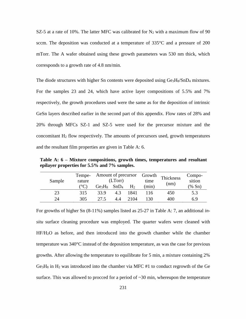
231
SZ-5 at a rate of 10%. The latter MFC was calibrated for N2 with a maximum flow of 90
sccm. The deposition was conducted at a temperature of 335°C and a pressure of 200
mTorr. The A wafer obtained using these growth parameters was 530 nm thick, which
corresponds to a growth rate of 4.8 nm/min.
The diode structures with higher Sn contents were deposited using Ge3H8/SnD4 mixtures.
For the samples 23 and 24, which have active layer compositions of 5.5% and 7%
respectively, the growth procedures used were the same as for the deposition of intrinsic
GeSn layers described earlier in the second part of this appendix. Flow rates of 28% and
20% through MFCs SZ-1 and SZ-5 were used for the precursor mixture and the
concomitant H2 flow respectively. The amounts of precursors used, growth temperatures
and the resultant film properties are given in Table A: 6.
For growths of higher Sn (8-11%) samples listed as 25-27 in Table A: 7, an additional in-
situ surface cleaning procedure was employed. The quarter wafers were cleaned with
HF/H2O as before, and then introduced into the growth chamber while the chamber
temperature was 340°C instead of the deposition temperature, as was the case for previous
growths. After allowing the temperature to equilibrate for 5 min, a mixture containing 2%
Ge3H8 in H2 was introduced into the chamber via MFC #1 to conduct regrowth of the Ge
surface. This was allowed to procced for a period of ~30 min, whereupon the temperature
Table A: 6 – Mixture compositions, growth times, temperatures and resultant
epilayer properties for 5.5% and 7% samples.
Sample
Tempe-
rature
(°C)
Amount of precursor
(LTorr) Growth
time
(min)
Thickness
(nm)
Compo-
sition
(% Sn) Ge3H8 SnD4 H2
23 315 33.9 4.3 1841 116 450 5.3
24 305 27.5 4.4 2104 130 400 6.9
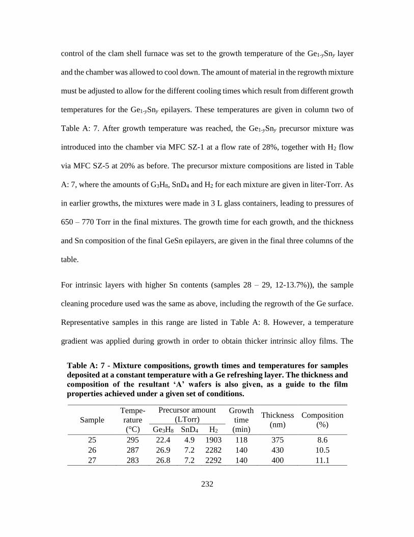
232
control of the clam shell furnace was set to the growth temperature of the Ge1-ySny layer
and the chamber was allowed to cool down. The amount of material in the regrowth mixture
must be adjusted to allow for the different cooling times which result from different growth
temperatures for the Ge1-ySny epilayers. These temperatures are given in column two of
Table A: 7. After growth temperature was reached, the Ge1-ySny precursor mixture was
introduced into the chamber via MFC SZ-1 at a flow rate of 28%, together with H2 flow
via MFC SZ-5 at 20% as before. The precursor mixture compositions are listed in Table
A: 7, where the amounts of G3H8, SnD4 and H2 for each mixture are given in liter-Torr. As
in earlier growths, the mixtures were made in 3 L glass containers, leading to pressures of
650 – 770 Torr in the final mixtures. The growth time for each growth, and the thickness
and Sn composition of the final GeSn epilayers, are given in the final three columns of the
table.
For intrinsic layers with higher Sn contents (samples 28 – 29, 12-13.7%)), the sample
cleaning procedure used was the same as above, including the regrowth of the Ge surface.
Representative samples in this range are listed in Table A: 8. However, a temperature
gradient was applied during growth in order to obtain thicker intrinsic alloy films. The
Table A: 7 - Mixture compositions, growth times and temperatures for samples
deposited at a constant temperature with a Ge refreshing layer. The thickness and
composition of the resultant ‘A’ wafers is also given, as a guide to the film
properties achieved under a given set of conditions.
Sample
Tempe-
rature
(°C)
Precursor amount
(LTorr) Growth
time
(min)
Thickness
(nm)
Composition
(%) Ge3H8 SnD4 H2
25 295 22.4 4.9 1903 118 375 8.6
26 287 26.9 7.2 2282 140 430 10.5
27 283 26.8 7.2 2292 140 400 11.1

233
growth of the intrinsic Ge1-ySny layer was initiated as above by introducing the precursor
mixture into the growth chamber at a suitable growth temperature. The growth was allowed
to proceed at this temperature for 45-60 min, with the aim of creating a strain relaxed seed
layer suitable for further growth. Thereafter, the chamber temperature was slowly increased
by 5-10°C over a period of 10-30 min. The growth was then allowed to proceed to
completion at the higher temperature. The chamber pressure during growth as maintained
at 200 mTorr. The thickness and composition properties of the films obtained following
this procedure are given in last two columns of Table A: 8. The second and third columns
of the same table lists the initial and final temperatures used in each growth. Columns 4-6
give the amounts of germanium and tin precursors and H2 carrier gas used in each mixture,
which was made in a 3 L container. The final mixture pressure is ~770 Torr, and it was fed
into the chamber via MFC SZ-1 at a flow rate of 28%. A concomitant H2 flow was also
maintained, as was the case in earlier growths.
In conclusion, this section outlines the growth parameters which can be used to synthesize
intrinsic GeSn alloys on n-type doped Ge/Si substrates which can be used as active layers
of n-Ge/i-Ge1-ySny/p-Ge1-zSnz diodes.
Table A: 8 – Mixture composition, growth time and thickness for device stack
intrinsic layers grown with the temperature ramp method. The thickness and
composition of the ‘A’ wafers are given as a guide to the achievable film
parameters.
Sample
Temperature
(°C)
Precursor amount
(LTorr) Growth
time
(min)
Thick-
ness
(nm)
Compo-
sition
(%) Initial Final Ge3H8 SnD4 H2
28 280 288 26.9 8.6 2330 143 360 12.0
29 270 280 26.4 10.0 2320 142 430 12.8
30 273 278 26.3 9.9 2326 142 335 13.7

234
Growth of n-type doped layers for pn junction diodes
By following the temperature gradient growth method described above for samples 28-30,
it was possible to obtain thick, strain relaxed films. Such films can be n-type doped as the
first step in the fabrication of pn junction diodes with compositions above indirect-direct
crossover. These films were deposited on intrinsic virtual Ge substrates which were
quartered and subjected to a HF clean as described earlier. Thereafter the wafers were
introduced into the single zone CVD reactor, where the Ge surface was subjected to
regrowth. The growth of the n-type doped epilayer was initiated by introducing the
precursor mixture consisting of Ge3H8, SnD4, P(SiH3)3 and H2 into the growth chamber via
MFC SZ-1 at a flow rate of 28%. Concomitant H2 flow was maintained at a rate of 20%
via MFC SZ-5. The procedure for temperature variation during growth was similar to that
describe earlier intrinsic Ge1-ySny epilayers. The temperature ranges used for the
representative samples is given in the second and third columns of Table A: 9, together
with amounts of precursors used for growth mixtures listed in the next three columns. The
final column of Table A: 9 gives the growth time for each epilayer.
The properties of the resultant films are listed in Table A: 10, which gives the film
thickness, Sn content and active donor concentration for the various epilayers. This data
Table A: 9 – Growth temperatures, times and mixture compositions for n-type
doped samples grown using the temperature gradient method.
Sample Temperature (°C) Mixture contents (LTorr) Growth
Time (min) Initial Final Ge3H8 SnD4 P(SiH3)3 H2
31 287 295 27.12 7.26 0.31 2310 145
32 280 287 26.76 7.81 0.39 2297 145
33 280 287 26.80 8.82 0.14 2323 147
34 280 287 26.81 8.83 0.40 2316 142

235
provides a guide to the various types of films which can be obtained using the above
procedures.
Growth of p-type doped top contact layers
The p-type doped top contact layers required to complete the above device stacks were
deposited in the three zone UHV-CVD reactor. The conditions used for depositing p-type
layers for samples listed earlier in Tables A: 7, A: 8 and A: 10 are given in Table A: 11.
Prior to deposition, the surface of the structures which consist of the n-type (for pn diodes)
and intrinsic (for pin diodes) layers deposited using the methods described thus far were
cleaned using aqueous HF. The wafer loading procedure was identical to the one used when
depositing intrinsic Ge1-ySny alloys using Ge2H6 in the three zone reactor, which was
described earlier. After loading, the surfaces were subjected to an in-situ cleaning step
using Ge2H6. The growth of the p-type layers was initiated after this cleaning step by
introducing the mixtures consisting of Ge2H6 and SnD4 in to the chamber via MFC TZ-4
at a flow rate of 30%. A flow of research grade H2 was maintained throughout the growth,
as well as a flow of B2H6 diluted with H2 in order to achieve doping. The flow rate for the
Table A: 10 – Thickness, composition and active carrier concentrations obtained
in the ‘A’ wafers using the growth parameters listed in Table A: 9.
Sample Thickness
(nm)
Composition
(% Sn)
Doping
(/cm-3)
31 525 9.3 4.8×10¹⁸
32 325 11.2 2.7×10¹⁹
33 535 12.0 5.7×10¹⁸
34 480 11.9 2.0×10¹⁹
236
former was 10% via MFC TZ-2. The amounts of precursors used for the Ge2H6/SnD4
mixtures are given in the fifth and sixth and seventh columns of Table A: 11. The containers
used for this purpose typically had a volume of 1 L. The B2H6 mixture flow rate via MFC-
TZ1 (5 sccm / H2 calibration) was varied between different growths, as given in column 8
of the table. The mixture compositions are listed in columns 9 and 10, and were typically
made in 250 mL containers. The pressure used for all the depositions was 300 mTorr. The
growth times are also given in the table. The resultant p-type film compositions,
thicknesses and doping are described in Table A: 12. These layers are the final components
which complete the pn and pin device structures whose initial components were described
in previous sections.
Growth of diodes with n, i and p components consisting of GeSn
The first growth of a Si/Ge/n-Ge1-xSnx/i-Ge1-ySny/p-Ge1-zSnz diode stack was conducted on
an intrinsic virtual Ge substrate, which was prepared for epitaxy using the same cleaning
procedures used earlier. After loading the wafers into the single zone UHV-CVD chamber
a Ge spacer layer was deposited using Ge3H8 in order to regenerate the surface. Then, an
n-type layer of suitable thickness to be used as the bottom contact was deposited using a
mixture consisting of 28.0 LTorr of Ge3H8 and 3.7 LTorr of SnD4. The dopant was
introduced by including 0.3 LTorr of P(SiH3)3 in this precursor mixture, which was finally
diluted with H2. The mixture was made in a 3 L container, and the addition of 2160 LTorr
of H2 gave a final pressure of 720 Torr. The growth was started at 310°C in order to
promote strain relaxation, and slowly cooled to 305°C, a temperature more suitable for the

237
Tab
le A
: 11 –
Gro
wth
para
met
ers
for
p-t
yp
e la
yer
s.
Sam
ple
T
emper
ature
(°C
) G
eSn m
ixtu
re
conte
nts
(L
Torr
) D
ibora
ne
mix
ture
flow
rat
e (%
)
Dib
ora
ne
mix
ture
conte
nts
(L
Torr
) G
row
th
tim
e (m
in)
Zone
1
Zone
2
Zone
3
Ge 2
H6
SnD
4
H2
B2H
6
H2
22
315
345
345
17.0
3
0.6
2
153
8
2.6
3
20
20
23
310
330
330
18.7
1
1.4
1
168
8
2.5
0
18
21
24
310
330
330
18.4
8
1.4
2
166
8
3.8
2
18
24
25
305
330
330
18.0
2
1.4
3
162
8
3.6
0
19
20
26
305
325
325
18.1
5
1.7
8
163
8
3.7
6
19
25
27
273
293
293
34.1
6
4.5
1
307
25
3.7
1
19
46
28
273
293
293
34.1
6
4.5
1
307
25
3.7
1
19
46
29
260
280
280
40.5
2
3.3
1
365
25
3.5
5
19
56
30
270
290
290
33.7
6
4.6
8
304
21
3.6
0
19
45
31
270
290
290
32.3
7
3.7
3
291
20
3.6
3
19
45
32
265
285
285
31.8
8
3.7
4
287
20
3.5
7
19
39
33
275
295
295
33.2
6
2.4
0
299
20
2.1
9
20
44
34
265
285
285
31.9
4
4.0
0
287
25
3.7
8
19
30

238
growth of the target active layer composition of y=0.07. Upon completion of the n-layer
deposition, the growth chamber was flushed with H2 for a period of 5 min prior to the
commencement of the intrinsic layer growth. For the growth of this second layer, a 27.7
LTorr Ge3H8 and 4.8 LTorr SnD4 mixture diluted with H2 was employed. The mixture
container was again 3 L in volume, and therefore the final H2 pressure was 700 Torr. The
chamber pressure used for the deposition was 200 mTorr. After the growth of this n-i stack,
the sample was removed from the CVD chamber and the top p-type contact layer was
grown in the three zone UHV-CVD chamber using the same procedure used for previous
pin diodes. By using a mixture of 18.7 LTorr of Ge2H6 and 1.8 LTorr of SnD4 at a
temperature of 315°C, it was possible to lattice match the final epilayer to the n-i stack.
Characterization of the final n-i-p stack showed that the n-type layer has an active carrier
concentration of 3×1019 cm-3, a thickness of 410 nm and a Sn content of 6.0%. The intrinsic
layer is thicker, with a thickness of 550 nm, and has a Sn incorporation of 7.0%. The top
Table A: 12 – Thickness, doping and Sn contents of p-type doped layers deposited
using parameters listed in Table A: 11.
Sample Thickness
(nm)
Composition
(% Sn)
Doping
(/cm-3)
22 150 1.9 1.4×10¹⁹
23 150 4 7.9×10¹⁸
24 200 4.1 2.7×10¹⁹
25 150 5 9.1×10¹⁹
26 135 4.4 1.6×10¹⁹
27 250 4.8 8.9×10¹⁹
28 275 6 6.6×10¹⁹
29 140 10 3.4×10¹⁹
30 140 8.4 4.0×10¹⁹
31 300 8.6 2.4×10¹⁹
32 150 10.4 3.1×10¹⁹
33 100 7.7 3.0×10¹⁹
34 120 11.9 1.8×10¹⁹
239
layer has a Sn concentration of 6.0%, and the dopant level as measured by ellipsometry is
3×1019 cm-3. The thickness of the layer is 120 nm.
It was possible to obtain diodes with higher active layer Sn contents by increasing the Sn
composition of the n-type doped Ge1-xSnx layer. The samples which prove this concept
were deposited on an n-type doped virtual Ge substrate, which was cleaned and loaded into
the growth chamber following the same methods described earlier. After re-growing the
Ge surface, the n-type doped Ge1-xSnx layer was deposited using a mixture of 26.9 LTorr
of Ge3H8, 8.66 LTorr of SnD4, 0.146 LTorr of P(SiH3)3 and 2308 LTorr of H2. The growth
temperature for this layer was initially 280°C, but was increased to 287°C during the
growth. Resultant epilayers had thicknesses of 275 nm and 215 nm (A and B wafers
respectively), and a composition of ≈11-12% Sn. The carrier concentration of the layers
was 9×1018 cm-3.
The wafers were then removed from the growth chamber for characterization. Prior to re-
introducing them into the growth chamber, the surfaces were cleaned using HF/H2O. The
active layers were deposited starting at an initial temperature of 260°C. The temperature
was increased to 265°C during the course of the deposition. After depositing the intrinsic
layer for 115 min, B2H6 was introduced into the chamber via MFC SZ-4.1 (5 sccm / N2) in
order to dope the top layer p-type. The B2H6 mixture used for this purpose consisted of 4.1
LTorr of B2H6 and 20.9 LTorr of H2. The growth time for the p-doped layer was 25 min.
The intrinsic layer of the A wafer obtained from this procedure was 130 nm thick with a
composition of 15.1% Sn, while the B wafer was 16% Sn with a thickness of 120 nm. The
p-type layers were 60 nm and 55 nm respectively, while both films had the same

240
composition as the active layer. The active carrier concentrations were measured to be
~5×1019 cm-3.
The properties of all the device stacks deposited using the above methods are given in
Chapter 7.

241
APPENDIX B
PERMISSIONS FOR REPRINTED MATERIALS

242
This appendix contains licensing agreements and permissions for reprinted material used
in this dissertation. For all papers which have been reprinted, permission has been obtained
from all co-authors for use of the articles.

243
Xu, C.; Gallagher, J. D.; Wallace, P. M.; Senaratne, C. L.; Sims, P.; Menéndez, J.;
Kouvetakis, J. Semicond. Sci. Technol. 2015, 30 (10), 105028.

244
Kouvetakis, J.; Favaro, R.; Grzybowski, G. J.; Senaratne, C.; Menéndez, J.; Chizmeshya,
A. V. G. Molecular strategies for configurational sulfur doping of group IV semiconductors
grown on Si (100) using S (MH3)2 (M= Si, Ge) delivery sources: An experimental and
theoretical inquiry. Chem. Mater. 2014, 26 (15), 4447.

245
Xu, C.; Senaratne, C. L.; Kouvetakis, J.; Menéndez, J. Experimental doping dependence
of the lattice parameter in n-type Ge: Identifying the correct theoretical framework by
comparison with Si. Phys. Rev. B 2016, 93 (4), 041201.
As the author of an APS-published article, may I include my article or a portion of my
article in my thesis or dissertation?
Yes, the author has the right to use the article or a portion of the article in a thesis or
dissertation without requesting permission from APS, provided the bibliographic citation
and the APS copyright credit line are given on the appropriate pages.
-https://journals.aps.org/copyrightFAQ.html#thesis
246
Senaratne, C. L.; Gallagher, J. D.; Jiang, L.; Aoki, T.; Menéndez, J.; Kouvetakis, J. Ge1-
ySny (y=0.01-0.10) alloys on Ge-buffered Si: Synthesis, microstructure, and optical
properties. J. Appl. Phys. 2014, 116 (13), 133509.

247

248
Senaratne, C. L.; Gallagher, J. D.; Aoki, T.; Kouvetakis, J.; Menéndez, J. Advances in light
emission from group-IV alloys via lattice engineering and n-type doping based on custom-
designed chemistries. Chem. Mater. 2014, 26 (20), 6033.

249
Senaratne, C. L.; Gallagher, J. D.; Xu, C.; Sims, P.; Menendez, J.; Kouvetakis, J. Doping
of Direct Gap Ge1-ySny Alloys to Attain Electroluminescence and Enhanced
Photoluminescence. ECS Trans. 2015, 69 (14), 157. Copyright 2015, The Electrochemical
Society.

250
Gallagher, J. D.; Senaratne, C. L.; Sims, P.; Aoki, T.; Menéndez, J.; Kouvetakis, J.
Electroluminescence from GeSn heterostructure pin diodes at the indirect to direct
transition. Appl. Phys. Lett. 2015, 106 (9), 091103.

251
Gallagher, J. D.; Senaratne, C. L.; Xu, C.; Sims, P.; Aoki, T.; Smith, D. J.; Menéndez, J.;
Kouvetakis, J. Non-radiative recombination in Ge1−ySny light emitting diodes: The role of
strain relaxation in tuned heterostructure designs. J. Appl. Phys. 2015, 117 (24), 245704.

252

253
Gallagher, J. D.; Senaratne, C. L.; Wallace, P. M.; Menéndez, J.; Kouvetakis, J.
Electroluminescence from Ge1−ySny diodes with degenerate pn junctions. Appl. Phys. Lett.
2015, 107 (12), 123507.