chemistem™ technology a revolution in edx...
TRANSCRIPT

Application Note
ChemiSTEM™ TechnologyA revolution in EDX analytics
Application Note ChemiSTEMTM Technology
Page 2
ChemiSTEM™ Technology: A revolution in X-ray analyticsInformation about chemical composition on the nanoscale is pivotal for an understanding of nanostructures and devices, and X-ray spectrometry is a well-established, robust and easy to use technique to obtain this information. Better yet, in the Scanning/Transmission Electron Microscope (S/TEM), X-ray analysis pairs microstructural information obtained from high-resolution imaging with accurate chemical composition information. But there has been an historical limitation with X-ray systems for the S/TEM: they collect only about 1% of all X-rays generated by the electron beam passing through the very thin sample. Recently, as the desired spatial resolution of chemical analysis has become progressively greater, the X-ray signal has decreased due to fewer atoms excited in smaller analytical volumes (a consequence of smaller electron beams and thinner samples). This results in low signal strength, bringing about low sensitivity and hence long analysis times – until now.
ChemiSTEM™ technology has been developed at FEI over a 5-year period with the express purpose of removing the old barriers in performance, bringing orders-of-magnitude improvement in many key metrics, such as sensitivity and speed. This reduces analysis times from hours to minutes, and sample features and elements that previously remained hidden can now be detected easily. With this new technology, we believe X-ray analytics in the S/TEM is poised to experience a renaissance based on this new capability to answer scientific questions that have until today remained unanswered. We begin with an explanation of how ChemiSTEM technology is able to provide such breakthrough capabilities.
Introduction to EDX analytics and ChemiSTEM TechnologyModern X-ray analysis on the S/TEM employs a well-established technology called X-ray energy dispersive spectroscopy (EDX), that operates in the following manner: The electron beam ejects atomic core-shell electrons in the sample, and recombination of a higher shell electron into the now empty core state creates X-rays imprinted with this atom’s characteristic energy. The X-rays created in the sample are absorbed in a nearby semiconductor detector and the deposited X-ray energy creates between a few hundred to a few thousand electron-hole pairs, which are immediately separated and collected by the detector as a charge pulse. The fast electronics to accurately detect these pulses are robust and reliable, meaning they produce highly-repeatable results that are easily calibrated in energy. The pulse-processing electronics measures the area under each pulse (which gives an energy) and then each pulse is “binned” into an energy spectrum. As incoming pulses (“X-ray counts”) are binned in energy, a spectrum of characteristic peaks is accumulated and can be automatically labeled by the computer. As noted, this technology is simple to use and reliable, but suffers from the very small analysis volume and poor ~1% total collection efficiency of X-rays described above. FEI analyzed this limitation and realized that in order to create a game changing new capability, it would be necessary to achieve an orders-of-magnitude boost in the net X-ray count rate. Total improvements of, say, 30%, or even a factor of 2-3 increase would simply not be revolutionary. This challenge set a high bar, requiring all avenues of potential improvement to be explored.
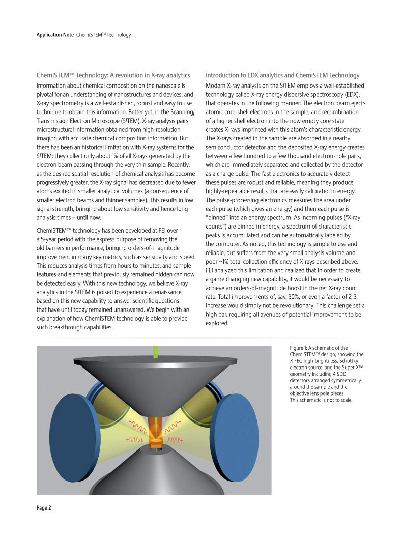
Figure 1: A schematic of theChemiSTEM™ design, showing theX-FEG high-brightness, Schottkyelectron source, and the Super-X™geometry including 4 SDD detectors arranged symmetrically around the sample and the objective lens pole pieces.This schematic is not to scale.
Application Note ChemiSTEMTM Technology
Page 3
It was clear a radically new X-ray detection system would be needed, but the FEI design team did not stop there. The net X-ray count rate depends on the count generation rate (set by the beam current), and the collection efficiency (set by the detector system). The ChemiSTEM system design is shown in Figure 1, and it addresses both needs: more beam current and more collection efficiency of X-rays. The higher beam current is provided by the proprietary X-FEG Schottky electron source. This FEI high-brightness gun can generate up to 5 times more beam current at a given spatial resolution compared to a conventional Schottky FEG source. The higher efficiency detection system is a radically new concept: it integrates 4 FEI-designed Silicon Drift Detectors (SDDs) very close to the sample area. These detectors are windowless to further boost collection efficiency and light element detection capability. This proprietary EDX design is called the Super-X™ system. Put in perspective, compared to conventional single-SDD, Schottky FEG systems, ChemiSTEM produces up to 5 times the X-ray generation with the X-FEG, and up to 10 times the X-ray collection with Super-X. Compared to conventional Si(Li) detector, Schottky FEG systems, there is another factor of several times speed enhancement due to the increased speed of the new SDD detectors. Figure 2 shows the results
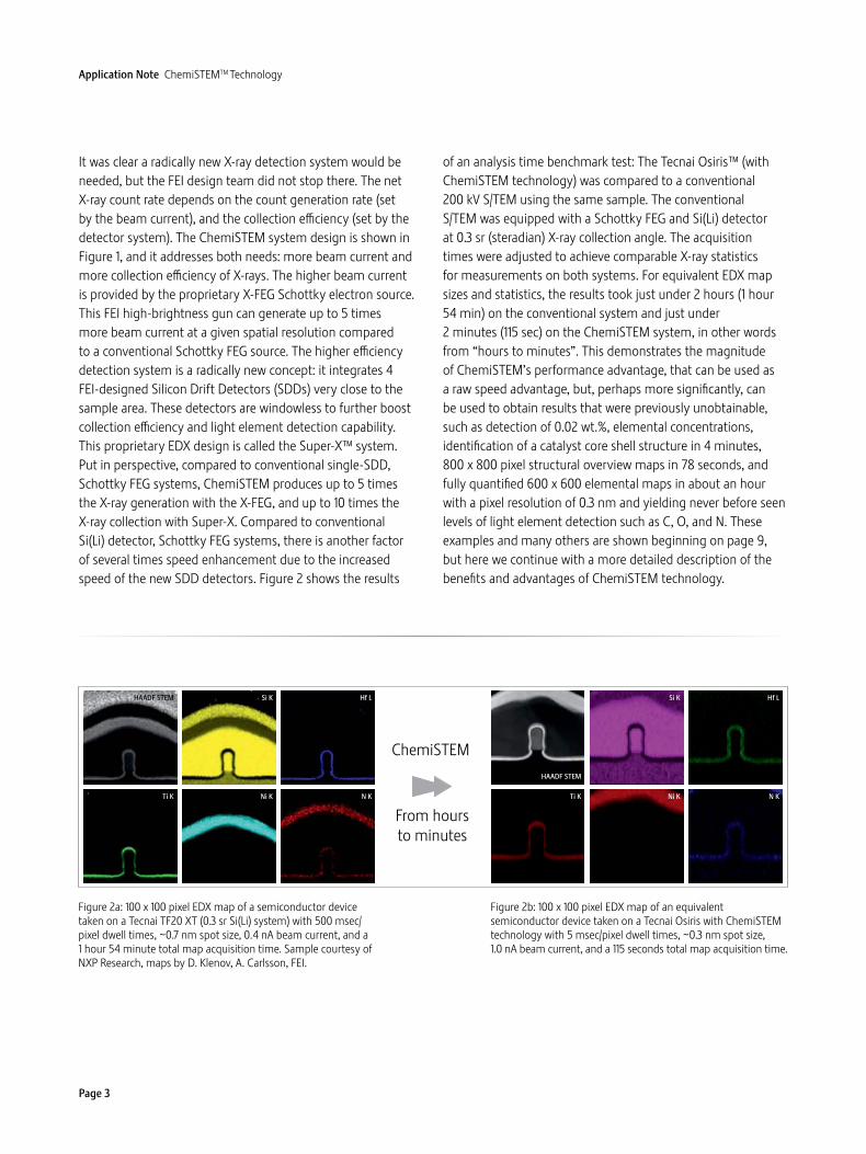
of an analysis time benchmark test: The Tecnai Osiris™ (with ChemiSTEM technology) was compared to a conventional 200 kV S/TEM using the same sample. The conventional S/TEM was equipped with a Schottky FEG and Si(Li) detector at 0.3 sr (steradian) X-ray collection angle. The acquisition times were adjusted to achieve comparable X-ray statistics for measurements on both systems. For equivalent EDX map sizes and statistics, the results took just under 2 hours (1 hour 54 min) on the conventional system and just under 2 minutes (115 sec) on the ChemiSTEM system, in other words from “hours to minutes”. This demonstrates the magnitude of ChemiSTEM’s performance advantage, that can be used as a raw speed advantage, but, perhaps more significantly, can be used to obtain results that were previously unobtainable, such as detection of 0.02 wt.%, elemental concentrations, identification of a catalyst core shell structure in 4 minutes, 800 x 800 pixel structural overview maps in 78 seconds, and fully quantified 600 x 600 elemental maps in about an hour with a pixel resolution of 0.3 nm and yielding never before seen levels of light element detection such as C, O, and N. These examples and many others are shown beginning on page 9, but here we continue with a more detailed description of the benefits and advantages of ChemiSTEM technology.
Figure 2a: 100 x 100 pixel EDX map of a semiconductor device taken on a Tecnai TF20 XT (0.3 sr Si(Li) system) with 500 msec/pixel dwell times, ~0.7 nm spot size, 0.4 nA beam current, and a 1 hour 54 minute total map acquisition time. Sample courtesy of NXP Research, maps by D. Klenov, A. Carlsson, FEI.
Figure 2b: 100 x 100 pixel EDX map of an equivalent semiconductor device taken on a Tecnai Osiris with ChemiSTEM technology with 5 msec/pixel dwell times, ~0.3 nm spot size, 1.0 nA beam current, and a 115 seconds total map acquisition time.
From hours to minutes
ChemiSTEM
HAADF STEM
Ti K
Si K
Ni K
Hf L
N K
HAADF STEM
Ti K
Si K
Ni K
Hf L
N K

Application Note ChemiSTEMTM Technology
Page 4
The Super-X advantage: Tilt responseA major advantage of the Super-X design comes from the large solid angle for X-ray collection provided by four SDD detectors symmetrically arranged around the specimen. But there is also an important advantage related to specimen tilting. Figure 3 compares measured X-ray count rates over a tilt range from –25° to +25°, for a Super-X system with 0.9 sr solid angle (red curve) and for a system with single Si(Li) detector with 0.3 sr solid angle (blue curve). The count rates were measured at 200 kV using standard commercially available NiOx test films with nominal thicknesses of 50 nm ± 10 nm and integrated over the entire energy range. The count rate is normalized to unity at the maximum response of the Super-X system, occurring at zero tilt angle. The Super-X response never drops below 80% of the maximum count rate over the entire tilt range. By contrast, the single detector system only achieves its maximum count rate when the sample is tilted strongly to +20° towards the single detector. At zero-tilt, the count rate is already reduced by 30% or more due to geometrical shadowing of the single detector by the sample holder, and at negative tilt angles, complete shadowing occurs at –10° where the response drops to zero. All one detector systems suffer from a similar undesirable tilt response, and
it occurs equally for SDD or Si(Li) detectors. The superior Super-X response occurs because at any tilt angle there are at least 2 detectors almost fully illuminated, and the 2 other detectors > 50% illuminated. Super-X response to beta tilt angles (not shown) is very similar to the response in Figure 3.
The ability to achieve high X-ray signal over a large portion of the S/TEM tilt space is a key performance improvement of the new system. Many studies in material science or chemistry require tilting to angles that cannot be easily controlled a priori due to the unknown orientation of nanoparticles or grain boundaries in poly-crystalline material. In these cases, the sample can be tilted to optimize imaging conditions and then does not need to be re-adjusted for optimum EDX analysis conditions. Conversely, for very many samples, an important crystal orientation to be observed is prepared to be very close to zero degrees tilt. For such samples, it is a key advantage to have the maximum X-ray response at zero tilt, as opposed to the ~30% reduction in response many systems experience due to detector shadowing at zero tilt. In these cases, it may not be feasible to tilt the sample towards the single detector to maximize response, due to the need to keep the beam parallel to a material interface (for an edge-on view).
-30 -20 -10 0
0.2
0.4
0.6
0.8
1.0
1.2
10 20 30Alpha tilt angle (degrees)
Nor
mal
ized
cou
nt ra
te
Super-X
Si(Li) 0.3 sr
-20 degreesbeam
Det. 3, 4 Det. 1, 2
Sample
-20 degrees
0 degrees
0 degrees
+20 degrees
+20 degrees
Figure 3: Comparison of relative EDX count rates of the Super-X system (on Tecnai Osiris with 0.9 sr collection angle) and a single Si(Li) detector system with 0.3 sr nominal solid angle. Both S/TEMs were operated at 200 kV with the same (constant) beam current. NiOx films were used as samples for both tilt series. Positive tilt angles represent specimen tilts towards the single detector for the Si(Li) system. Diagrams above the graph show the effects of detector shadowing for the 4 Super-X detectors, and diagrams below show shadowing effects for the single detector system.

Application Note ChemiSTEMTM Technology
Page 5
The Super-X advantage: Total response (1+1+1+1 > 4)
By simple logic, one expects the Super-X system with 4 detectors to be “4 times better” in response than a 1 detector system (i.e., “1+1+1+1 = 4”). However, this does not hold, because each individual Super-X SDD detector has significant design improvements in and of itself, compared to conventional individual SDD detector systems. So the response of each Super-X detector is “> 1”. How much greater is the question we now consider.
We now discuss two major design improvements of the individual detectors, leading to three distinct response improvement factors. First, as described earlier, since FEI designed the individual Super-X SDD detectors to be optimized for the FEI objective lens pole piece design (shape, size, geometry, etc.), we were able to completely eliminate the problem of detector shadowing at zero tilt angle. This means that the detector sits at a ‘take-off’ angle and location so that the detector is fully illuminated at zero tilt, with no shadowing loss. Achieving this required the design of a special sample holder, as well as optimized detector design.
Second, the Super-X detectors are windowless by design. The Super-X detectors instead have mechanical shutters that completely protect the detectors when they are not in live mode. This choice eliminates the need for ultra-thin polymer windows that are the source of two severe response losses for systems that do employ them. Figure 4 illustrates the effect of windows on X-ray collection efficiency, and there are two key effects to understand, which are illustrated by the diagram in Figure 4a. First, the polymer film itself is supported by a silicon support grid,
which blocks all X-rays hitting it and this results in a substantial X-ray response loss for all energies. Second, the polymer windows themselves, although transparent to X-rays >1 keV in energy, do have substantial absorption loss below 1 keV , particularly due to the carbon absorption edge around 300 eV, as seen in Figure 4b, which plots X-ray transmission efficiency for an SDD detector both with and without polymer windows. This figure shows that the efficiency loss due to windows (lower blue curve) is significant over the entire energy range, compared to a windowless system (upper red curve). The remaining loss in the windowless system below 1 keV is due to residual absorption by the thin Al electrode and Si dead layer at the front of the SDD detector. The windowless system has a factor of at least 2-3 greater efficiency at energies below 500 eV. This improvement in low energy X-ray collection efficiency has a huge impact on light element detection, as we will discuss in a later section.
We estimate that a typical conventional system has ~50% loss of its nominal solid angle response at zero tilt based on the several loss mechanisms we have discussed above. Thus, the expected zero-tilt efficiency increase of Super-X would be a factor of ~8: the 4 detectors plus an additional factor of ~2 to account for the 50% loss mechanisms above. This comparison assumes one detector of nominally equal solid angle to the individual Super-X detectors. Not included in this factor of 8 is the additional efficiency gained by Super-X at low energies below 1 keV, described above, due to the lack of polymer window absorption. Clearly, the exact efficiency enhancement over other systems depends on many factors of the detectors being compared and even the X-ray spectrum being measured (e.g. tilt angles employed, nominal solid angle differences, low energy enhancements, etc.).
0.1 102 3 4 5 6 7 2 3 4 5 2 3 4 56 671
Windowless SDD
SDD with ultra-thinpolymer window
0.4
0.2
0.8
1
0.6
X-ray Energy (keV)
Tran
smis
sion
Effi
cien
cy
Si grid bar
Window
Shadowing
Figure 4a: Schematic showing loss due to holder shadowing and detector window. Loss due to the window includes total absorption by the Si support grid bars (at all energies) and selective absorption by the polymer window (at energies below 1 keV). Figure 4b: X-ray transmission efficiency versus energy for a windowless SDD detector (red curve) and an SDD detector with thin polymer window (blue curve). Loss due to the both the Si grid bars and the polymer window contributes to the lower efficiency across all energies of the detector with window.
(a) (b)
Application Note ChemiSTEMTM Technology
Page 6
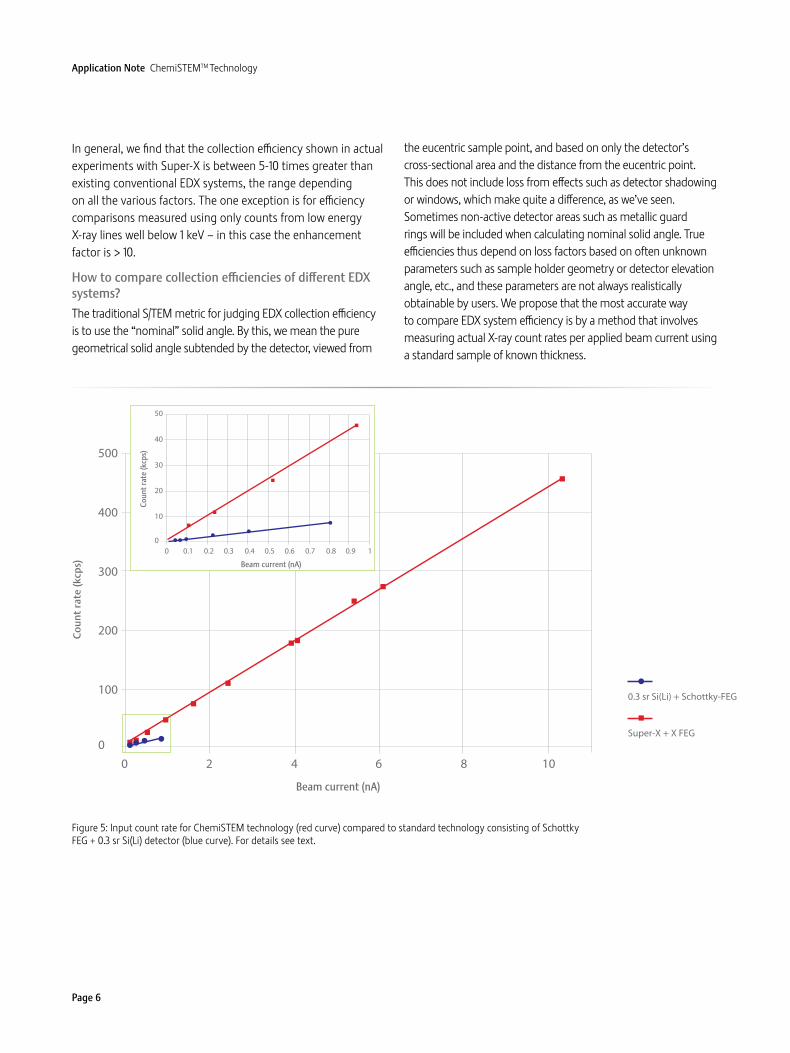
In general, we find that the collection efficiency shown in actual experiments with Super-X is between 5-10 times greater than existing conventional EDX systems, the range depending on all the various factors. The one exception is for efficiency comparisons measured using only counts from low energy X-ray lines well below 1 keV – in this case the enhancement factor is > 10.
How to compare collection efficiencies of different EDX systems? The traditional S/TEM metric for judging EDX collection efficiency is to use the “nominal” solid angle. By this, we mean the pure geometrical solid angle subtended by the detector, viewed from
the eucentric sample point, and based on only the detector’s cross-sectional area and the distance from the eucentric point. This does not include loss from effects such as detector shadowing or windows, which make quite a difference, as we’ve seen. Sometimes non-active detector areas such as metallic guard rings will be included when calculating nominal solid angle. True efficiencies thus depend on loss factors based on often unknown parameters such as sample holder geometry or detector elevation angle, etc., and these parameters are not always realistically obtainable by users. We propose that the most accurate way to compare EDX system efficiency is by a method that involves measuring actual X-ray count rates per applied beam current using a standard sample of known thickness.
0 2 4 6 8 10
0.3 sr Si(Li) + Schottky-FEG
Super-X + X FEG
200
100
0
400
500
300
Beam current (nA)
Cou
nt r
ate
(kcp
s)
0 0.1 0.2 0.3 0.4 0.5 0.6 0.7 0.8 0.9 1
0.3 sr Si(Li) + Schottky-FEG
Super-X + X FEG
20
10
0
40
50
30
Beam current (nA)
Coun
t rat
e (k
cps)
Figure 5: Input count rate for ChemiSTEM technology (red curve) compared to standard technology consisting of Schottky FEG + 0.3 sr Si(Li) detector (blue curve). For details see text.

Application Note ChemiSTEMTM Technology
Page 7
We have applied this comparison methodology and the results are shown in Figure 5. Input counts per second (cps) are plotted as a function of applied beam current for two S/TEM systems: A Tecnai Osiris with ChemiSTEM technology and a 200 kV S/TEM with Schottky FEG and Si(Li) detector of 0.3 sr nominal solid angle. The small inset shows the same data on a smaller scale closer to the origin. For both measurements, the same FIB-cut InP sample was measured and the X-ray counts were integrated over the full energy range. In order to be sure all measurements were taken on sites of the same thickness, EELS was employed to control sample thickness by measuring t/λ (thickness in relation to average mean free path). The first observation from this figure is that the ChemiSTEM system on Tecnai Osiris achieves more than 5 times the X-ray count rate per unit applied beam current than the conventional system, even though this system is an 0.3 sr nominal solid angle EDX system, which is considered at the high end of collection performance for conventional detectors. The second observation from Figure 5 is that more than 10 times higher beam currents can be applied for the ChemiSTEM system with the X-FEG gun, without saturation of the new Super-X detector system. At an applied beam current of 10 nA the input X-ray count rate is over 400,000 cps at approximately a 50% dead time of the Super-X detector system, meaning that the output X-ray count rate is over 200,000 cps at this value of applied current. The Super-X system has significantly higher input bandwidth for high count rates compared to systems with only one high-speed SDD detector, and thus the Super-X system can operate at 400,000 cps input count rate without significant degradation of energy resolution, which is not the case for systems with only one high-speed SDD detector.
The ChemiSTEM advantage: Light element sensitivityPoor detection of light elements (such as C, O, and N) has always been considered one of the big weaknesses of EDX as a technique, but ChemiSTEM technology removes this barrier to light element sensitivity. As shown in figure 4, the relative sensitivity of the windowless system for low energy X-rays in 500 eV or lower range is several times higher than systems with ultra-thin polymer windows. When this low-energy advantage is combined with the 5-10 times collection advantage of the Super-X system, it leads to an orders-of-magnitude boost in light element detection performance.
In Figure 6 we show measured data to demonstrate that the enhanced low energy performance shown Figure 4 is realized in the Super-X system. The figure shows a spectra from a NiOx film measured on the windowless Super-X system and a conventional EDX system with ultra-thin polymer windows. The count rates of both spectra have been normalized (set equal) at the Ni-K line at 7.4 keV in order to demonstrate only the relative differences in low energy efficiency. One can then see the advantage of the windowless system by noting the higher counts in the Ni-L, O-K, and C-K lines below 1 keV. The relative peak height is more than 2 times greater for oxygen at 528 eV and more than 3 times greater for carbon at 282 eV than for the system with polymer windows. We stress that this comparison does not include the primary Super-X collection efficiency increase (which is energy independent) since this has been removed in Figure 6 by the normalization. For a dramatic demonstration of the ChemiSTEM light element performance, see the C, N , and O maps shown in the PMOS transistor structure example found later in this note.
0 1 2 3 4 5 6 7 8
35,000
40,000
Windowless SDD
Si(Li) with ultra-thinpolymer window
30,000
25,000
20,000
15,000
10,000
5,000
0
Energy (keV)
Norm
alize
d co
unts
O
C
Ni-L
Ni-K
Figure 6: Comparison of a single windowless SDD with a standard Si(Li) detector with ultra-thin polymer window. The two spectra have been normalized to each other at the Ni-K line so that relative differences in the energy range below 1 keV are apparent.

Application Note ChemiSTEMTM Technology
Page 8
Ultimate sensitivity: Detection of low concentrationsThe improved performance of this new technology can be turned into a huge speed benefit (“hours to minutes”) as we have demonstrated, but the improved performance can also be used to achieve much higher sensitivities than were previously possible. This benefit is ultimately perhaps more important than speed, because it allows the detection of hidden features and elements that previously could not be seen. The ultimate test of EDX raw sensitivity is the ability to detect very low concentrations of elements, for example, well below 1 wt.% (weight %).
In Figure 7 we show the results of an experiment demonstrating the sensitivity limits of ChemiSTEM technology. This figure shows the EDX spectrum of a certified NIST steel standard (Standard Reference Material NBS No. 461). In bulk, this low-alloy steel has certified concentrations of the following elements: arsenic (0.028 wt.%), vanadium (0.024 wt.%), and tin (0.022 wt.%). Although this sample was prepared for TEM analysis using an FIB, it is expected that minimal changes have resulted in the composition. The full spectrum in Figure 7 was acquired in 600 seconds using a beam current of 1.7 nA while scanning a micron-sized area in order to average the composition over the microstructure of the steel.
The 3 smaller zoomed spectra at the bottom of Figure 7 show clear peaks from these 3 elements (V, As, and Sn) all of which have substantially good signal-to-noise ratio (Ga and Pt peaks visible are due to the FIB preparation process). This clearly demonstrates that the ChemiSTEM technology on Tecnai Osiris is capable of detecting low concentrations such as the ~0.02 wt.% concentrations in this certified NIST steel sample, obtained in a reasonable 10 minutes total acquisition time.
Whether your applications call for using the ultimate speed benefits of ChemiSTEM technology (mapping in “hours to minutes”, or huge area maps with unprecedented sensitivity in reasonable times), or the pursuit of ultimate sensitivity (pushing to detection of ultra-low concentrations or hidden sample features) we believe ChemiSTEM will give you the capability to answer many questions that were until now unresolved. In the following pages of this note, we show application data from the ChemiSTEM technology on Tecnai Osiris, covering many different types of material systems. We hope that this note has been a useful introduction to ChemiSTEM technology, and we invite you to contact us at FEI for further information on this new and exciting capability.
Figure 7: Super-X spectrum of NIST steel standard NBS No.461 (log scale), Bottom: zoomed spectra showing minor elements of vanadium (0.024 wt.%), arsenic (0.028 wt.%) and tin (0.022 wt.%). Ga and Pt peaks are due to FIB preparation.
Coun
tsCo
unts
Energy (keV)Energy (keV) Energy (keV)
Energy (keV)
Coun
ts
Coun
ts

Application Note ChemiSTEMTM Technology
Page 9
Fast acquisition of large mapsDue to the increased sensitivity of Super-X and the higher brightness of the X-FEG, it is has become possible to acquire large area maps with high spatial resolution. This allows users to adopt new and more efficient methods of sample examination. For example, instead of trying to understand elemental distribution from the images and then confirm it by point analysis or line profile acquisitions, it is now possible to acquire a large map with the speed of a STEM image and then proceed with a more careful analysis. This minimizes the
time needed to understand geometry of the sample, as well as allows for better understanding of the macroscopic structure of the sample. Another important advantage of high speed mapping is the minimization of the beam damage. Often samples will not be able to survive an exposure of the beam for longer than 100 μsec. Using fast iterative mapping prevents damage and allows for more accurate post acquisition analysis of the chemical composition.
Figure 8: These 800 x 800 pixel maps show the whole FIB lamellae and were mapped with ChemiSTEM in just 74 seconds using 100 μsec/pixel dwell time. This exposure is similar to just acquiring a couple of STEM images, and the resolution of the maps is actually equal or better than some of the HAADF STEM images. Note that even with such a short mapping time it is not only possible to identify distribution of the heavy elements like W, but also to see the distribution of elements like N and O - usually troublesome for EDX. This light element sensitivity is possible due to the windowless design of Super-X. Sample courtesy IME, Singapore.
HAADF STEM
Al-K
N-K
Si-K
O-K
W-L
2 mm

Application Note ChemiSTEMTM Technology
Page 10
45 nm PMOS transistor structure: Large Maps, All ElementsDevelopment of semiconductor devices requires measuring the distribution of all elements being present in the device structure in order to be able to monitor process success and quality. In that respect semiconductor devices are demanding since they contain heavy elements like tungsten (W), tantalum (Ta) and hafnium (Hf) as well as light elements down to nitrogen (N) and oxygen (O) and even sometimes carbon (C). This example of a 45 nm PMOS transistor structure demonstrates the advantages of ChemiSTEM technology. First, with its increased sensitivity for light elements, now virtually all elements of the periodic system can be detected in one EDX map acquisition. Second, these maps were acquired with an 0.3 nm pixel resolution, over a large field-of-view of about 190 nm in width. This high-resolution, high field-of-view combination is only possible due to the high-brightness of the X-FEG source. One can really appreciate the advantages of ChemiSTEM technology by looking at the unprecedented sensitivity and resolution seen in the light element maps, such as oxygen and nitrogen.
Figure 9: 600 x 600 pixel maps of a 45 nm PMOS transistor structure recorded with 50 μsec dwell time/pixel and 1 nA beam current. Drift correction was applied to acquire multiple frames in 100 minutes. The maps were fully quantified to eliminate contributions from overlapping peaks. Data courtesy by D. Klenov, FEI
50 nm

Application Note ChemiSTEMTM Technology
Page 11

Application Note ChemiSTEMTM Technology
Page 12
SuperconductorsNb3Sn superconducting cables are promising for applications in NMRs and Tokamak fusion reactors. Their use could provide higher current density at lower cost than current solutions. It is important, however, to know their chemical composition, since it impacts the superconducting properties.
Overview maps were taken from the cross section of the Nb3Sn superconducting multifilament cable (Figure 10). The Sn map clearly shows a variation in composition of the superconducting phase which influences the critical current densities. The compositional changes are caused by the initial interdiffusion of the Sn into the Nb filament from the bronze matrix. This allows direct identification of the areas of the best composition for the superconductivity.
The analysis also shows that Cu from the filament cladding interdiffuses into the Nb3Sn filament along the grain boundaries (see Figure 11). Although there is only a tiny amount of Cu (not soluble in Nb3Sn) at the grain boundary, it is possible to detect it. The map also shows the variation of the Sn and Nb composition in the grains.
Figure 11: 400 x 400 pixel maps recorded with 4 msec dwell time/pixel, 2.5 nA beam current and 1-1.3 nm spot size in 11 minutes. Maps show elements using integrated intesities. Sample courtesy: Marco Cantoni (EPFL Lausanne, Switzerland)
Figure 10: 400 x 400 pixel maps recorded with 4 msec dwell time/pixel, 2.5 nA beam current and 1-1.3 nm spot size in 11 minutes. Maps show elements using integrated intesities.Sample courtesy: Marco Cantoni (EPFL Lausanne, Switzerland)
Application Note ChemiSTEMTM Technology
Page 13
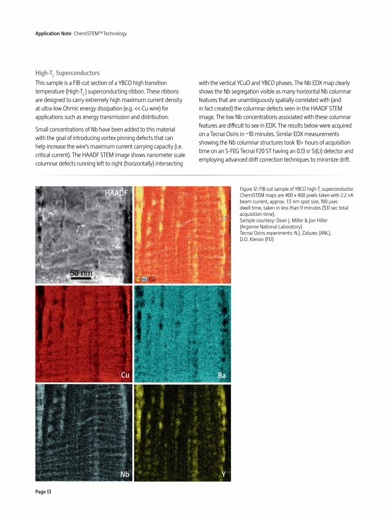
High-TC SuperconductorsThis sample is a FIB-cut section of a YBCO high transition temperature (High-TC) superconducting ribbon. These ribbons are designed to carry extremely high maximum current density at ultra-low Ohmic energy dissipation (e.g. << Cu wire) for applications such as energy transmission and distribution.
Small concentrations of Nb have been added to this material with the goal of introducing vortex pinning defects that can help increase the wire’s maximum current carrying capacity (i.e. critical current). The HAADF STEM image shows nanometer scale columnar defects running left to right (horizontally) intersecting
with the vertical YCuO and YBCO phases. The Nb EDX map clearly shows the Nb segregation visible as many horizontal Nb columnar features that are unambiguously spatially correlated with (and in fact created) the columnar defects seen in the HAADF STEM image. The low Nb concentrations associated with these columnar features are difficult to see in EDX. The results below were acquired on a Tecnai Osiris in ~10 minutes. Similar EDX measurements showing the Nb columnar structures took 10+ hours of acquisition time on an S-FEG Tecnai F20 ST having an 0.13 sr Si(Li) detector and employing advanced drift correction techniques to minimize drift.
Figure 12: FIB-cut sample of YBCO high-Tc superconductor. ChemiSTEM maps are 400 x 400 pixels taken with 2.2 nA beam current, approx. 1.5 nm spot size, 100 μsec dwell time, taken in less than 9 minutes (531 sec total acquisition time).Sample courtesy: Dean J. Miller & Jon Hiller (Argonne National Laboratory)Tecnai Osiris experiments: N.J. Zaluzec (ANL), D.O. Klenov (FEI)
HAADF
Cu
Y
Ba
Nb

Application Note ChemiSTEMTM Technology
Page 14
MetallurgyIn this example, the power of ChemSTEM is applied to study the chemical composition of metal alloys with phase segregation. With phase separation and intergrowth on the nanoscale the mechanical properties of alloys can be tuned in order to achieve desired macroscopic structural properties. In this example the intergrowth of WB into TiB2 improves the hardness of pure TiB2 dramatically. Intergrowth of orthorhombic WB in hexagonal TiB2 is enhanced by doping of CrB2 into the material. The chromium increases the mobility of the boron lattice to enable the intergrowth of the monoboride (WB) in the diboride matrix (TiB2). The WB is growing along the
prism planes of the hexagonal TiB2 matrix, creating a hexagonal pattern in the HAADF images in STEM. The HAADF images show the complexity of the intergrowth on the mesoscopic (Figure 13) and on the atomic level (Figure 14). The smallest WB layers are of the size of a unit cell of WB, which is around 0.8 nm. In the chemical maps the WB layers can clearly be resolved in the W and Ti map. The smallest lines correspond to a single unit cell of WB. The chromium map reveals the enrichment of the chromium around the WB. The concentration of the chromium is extremely low since only 5% of CrB2 was added macroscopically to the compound to stimulate the WB growth.
Figure 13: ChemiSTEM maps on WB/TiB2/CrB2 compound. HAADF image with chemical map of chromium, tungsten and titanium. All images are acquired simultaneously. Map size is 512 x 512 pixels acquired with 50 μsec dwell time/pixel, 20 min total mapping time, and 1 nm spot size. Structures as small as 0.8 nm are visible in the chemical maps.
Figure 14: HAADF STEM image demonstrating that the thinnest layers of WB are only one unit cell of the orthorhombic structure in width, which corresponds to 0.8 nm. Some of these 8 Angstrom structures are clearly visible in the chemical maps.
HAADF
Ti
Cr
W
1 mm

Application Note ChemiSTEMTM Technology
Page 15
Ceramics: Porous alumina/titania nanocompositeNanostructured titania is highly attractive for a number of current and potential chemical, optical, and biomedical applications. A proprietary fabrication process, under development by the School of Materials Science and Engineering, Georgia Institute of Technology, in collaboration with U.S. Air Force Research Laboratory, has been used to synthesize titania-coated porous alumina nanocomposite structures. The X-ray maps shown in these images, obtained by the Department of Materials Science and Engineering, The Ohio State University, with ChemiSTEM technology on the
Tecnai Osiris, reveal the controlled distribution of titanium, aluminum, oxygen, and phosphorus in the titania/alumina-based composites. Such high-resolution X-ray mapping provides a key capability for correlating processing changes to nanoscale structures and chemistries. This research is being conducted within the BIONIC (Bio-nano-enabled Inorganic/Organic Nanocomposites and Improved Cognition) Air Force Center of Excellence, which involved collaborators at the Georgia Institute of Technology, The Ohio State University, and the Air Force Research Laboratory.
Figure 15: 512 x 512 pixel maps recorded with 50 μsec dwell time/pixel, 1.4 nm spot size, and 2.2 nA beam current in less than 6 minutes (327 sec).Courtesy of the following cooperation: T. McLachlan, Y. Cai, and K. H. Sandhage (Georgia Tech), D. Huber, R. Williams, and H. Fraser (Ohio State), N.J. Zaluzec (ANL) and M. Durstock and R. Vaia (Air Force Research Lab)
HAADF
500 nm
P
O
Ti
Al
Al P Ti map

Application Note ChemiSTEMTM Technology
Page 16
Catalysis and NanoparticlesChemiSTEM technology enables monitoring nanoparticles as small as 1 nm in diameter. Therefore it can be used to check quality and repeatability of different routes to produce nanoparticles even if their size reaches down to the 1 nm level. Figure 16 shows Au particles on carbon substrate with particle sizes varying between 1 and 2 nm.
Mapping very small nanoparticles is an important application but sometimes it is necessary to distinguish nanoparticles or clusters of different composition. This can be achieved using HAADF STEM images since their contrast strongly depends on the atomic number Z of the elements. However, it is almost impossible to distinguish particles with different composition from HAADF STEM images when the elements’ atomic numbers are relatively close (as seen on the HAADF STEM image in Figure 17). In this case ChemiSTEM technology successfully identified the different metals (Au, Ag, Co, Pd, Pt) which are displayed in the RGB image.
Figure 17: Comparison of HAADF STEM imaging (left) with elemental mappings (RGB on the right) extracted from STEM-EDX experiments. Different metals can be clearly distinguished. Sample courtesy of P. Hozak, Institute of Molecular Genetics, Prague, Czech Republic.
Figure 16: Specimen courtesy of NANOGAP, Spain (http://www.nanogap.es) and the NANOMAG group (http://www.nanomag.org) of the University of Santiago de Compostela, Spain.
100 nm
HAADF
Application Note ChemiSTEMTM Technology
Page 17
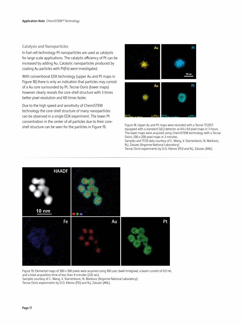
Catalysis and NanoparticlesIn fuel cell technology Pt nanoparticles are used as catalysts for large scale applications. The catalytic efficiency of Pt can be increased by adding Au. Catalytic nanoparticles produced by coating Au particles with Pt(Fe) were investigated.
With conventional EDX technology (upper Au and Pt maps in Figure 18) there is only an indication that particles may consist of a Au core surrounded by Pt. Tecnai Osiris (lower maps) however clearly reveals the core-shell structure with 3 times better pixel resolution and 60 times faster.
Due to the high speed and sensitivity of ChemiSTEM technology the core-shell structure of many nanoparticles can be observed in a single EDX experiment. The lower Pt concentration in the center of all particles due to their core-shell structure can be seen for the particles in Figure 19.
Figure 19: Elemental maps of 300 x 300 pixels were acquired using 100 μsec dwell time/pixel, a beam current of 0.9 nA, and a total acquisition time of less than 4 minutes (226 sec).Samples courtesy of C. Wang, V. Stamenkovic, N. Markovic (Argonne National Laboratory);Tecnai Osiris experiments by D.O. Klenov (FEI) and N.J. Zaluzec (ANL).
Figure 18: Upper Au and Pt maps were recorded with a Tecnai TF20ST equipped with a standard Si(Li) detector as 64 x 64 pixel maps in 3 hours. The lower maps were acquired using ChemiSTEM technology with a Tecnai Osiris: 200 x 200 pixel maps in 3 minutes. Samples and TF20 data courtesy of C. Wang, V. Stamenkovic, N. Markovic, N.J. Zaluzec (Argonne National Laboratory)Tecnai Osiris experiments by D.O. Klenov (FEI) and N.J. Zaluzec (ANL).
HAADF
Fe Au Pt

Application Note ChemiSTEMTM Technology
Page 18
Thin film / multilayer structures: Quantifying light elementsThe large improvement in chemical sensitivity allows better high-accuracy quantification of all elements for mapping and line profile analysis. One traditional challenge for EDX quantification is to distinguish elements with strong peak overlaps, as is the case in this example with Ti and N (Ti-L strongly overlaps with N-K). The maps in Figure 20 show a sample with Ti/TiN multilayers separating Al from SiO2. In this case using quantification the Ti and TiN layers are easily differentiated. Despite the large pixel count of such a map, note that each pixel has a fully recorded complete spectra with good statistics for quantification. This means that all elements can be quantified and displayed after the data is obtained. For example, it is possible to see that the non-uniformity in the Ti layer are cause by interdiffusion of the Al and the Ti (see red arrows in Ti and Al map). This would not be so straightforward to do with techniques like EFTEM.
Figure 20: Thin film structure with Ti/TiN multilayers separating SiO2 from Al. Map parameters: 400 x 400 pixels, 50 μsec/pixel dwell time, multiple frames, 11 min total acquisition time, beam current 2.3 nA. Sufficient X-ray spectra statistics for full quantification without binning. Sample courtesy IME, Singapore.
Figure 21: Line profile of the Ti/TiN multilayer with 0.5 sec dwell time per point and 1.5 nA beam current. Quantified profile shows that that the oxygen distribution in the area of Ti and Al interdiffusion is non-zero. Even for oxygen concentrations near 1% this effect is still seen, despite the heavy peak overlap of Ti, N, and O shown in the spectra (taken from the point marked by the cross). Despite the fact that light elements are considered the strength of EELS and usually a challenge for EDX, in this case EELS struggles to quantify the same oxygen concentration due to the complexity of background subtraction. Sample courtesy IME, Singapore.

Application Note ChemiSTEMTM Technology
Page 19
Compound Semiconductor / Quantum WellsInGaN quantum wells are widely used in light emitting devices, and the composition of the wells (in particular the In concentration) controls the frequency of the emitted light. Traditionally, the TEM could provide information about the geometry and atomic structure of the layers, however, the In concentrations were always difficult to measure due to high sensitivity of the material to electron damage. The high
detection sensitivity of the ChemiSTEM technology permits data acquisition allowing the In concentration to be quantified for this sample, due to orders of magnitude shorter required pixel dwell times for quantification. Nominal composition of In in the alternating layers was approximately 10%, 18%, and 26% with two sets of layers having this nominal composition.
Figure 23: Fast ChemiSTEM mapping used to show the elemental distribution around a surface defect in less than 5 minutes. Map size 525 x 230 pixels, 50 μsec dwell time, multiple frames (iterative mapping), 276 sec total acquisition time, 1.7 nA beam current. Integrated intensities used to show elemental distribution.
HAADF N O AI Ga In
Figure 22: EDX lineprofile across all layers with full quantificationperformed. 1000 points, 0.5 sec dwell time, 0.25 nA beam current.The differences in composition between different layers are clearly quantifiable.

World HeadquartersPhone: +1.503.726.7500
FEI Europe Phone: +31.40.23.56000
FEI Japan Phone: +81.3.3740.0970
FEI Asia Phone: +65.6272.0050
© 2010. We are constantly improving the performance of our products, so all specifications are subject to change without notice.Technai Osiris, ChemiSTEM, Super-X and the FEI logo are trademarks of FEI Company, and FEI is a registered trademark of FEI Company. All other trademarks belong to their respective owners.
See Beyond at FEI.com
AN0027 07-2010
Application Note ChemiSTEMTM Technology
ChemiSTEM™ technology is now introduced on Tecnai Osiris™
Main EDX-related Specifications:
r X-FEG Brightness
1.8 x 10⁹ A/cm2/sr (@200 kV)
r X-FEG probe current
0.4 nA in 0.31 nm spot (@200 kV)
1.5 nA in 1 nm spot (@200 kV)
r Fast mapping: dwell time/pixel down to 10 μs
r Output count rate: up to 200 kcps
r Solid angle: 0.9 sr
r Energy resolution
< 136 eV @ Mn-Kα and 10 kcps (output)
< 140 eV @ Mn-Kα and 100 kcps (output)
r High P/B ratio (Fiori number): > 4,000
r Excellent EDX in-hole performance
< 1% hole-counts
r Low system background in EDX
< 1% spurious peaks
For more details see Tecnai Osiris product data sheet