“cher ami” project
TRANSCRIPT

“Cher Ami” Project
Progress Report II of EE Group Team 3
Date: 16.12.2011
Authors:
Oğuzhan Avcı (HW Engineer)
Abdullah Başar Akbay (HW Engineer)
Version I

2
Table of Contents
1. Preliminary Design Explanation 3
1.1 Bluetooth Module SCC 001-002
3
1.2 FPGA Chip SCC 001-003 5
1.3 Power Supply SCC 001-004 6
2. Technology Demonstration Test Plan 8
3. Conclusion 10
4. References 13

3
1. Preliminary Design Explanations In Cher Ami hardware, there exist three sub modules which are defined in Preliminary
Report as Bluetooth Module, FPGA Chip and Power Supply. In Preliminary Design
Report, features of these sub modules and the relationships between these sub modules
are explained in detail. In this part of Progress Report II of EE Group, the logics behind
these designs are discussed.
1.1 Bluetooth Module SCC 001-002
Objective of the Bluetooth module is maintenance of the wireless Bluetooth
communication channel between FPGA Chip (SCC 001-003) and mobile phone. SCC 001-
002 Bluetooth Module consists of TI CC2540 2.4GHz Bluetooth Low Energy System-on-
Chip Solution and its application circuitry.
Main motivation behind the choice of TI CC2540 is that EE Group already has a TI
CC2540 mini development kit. Hardware group engineers are inexperienced in
Bluetooth telecommunication implementation; therefore, this development kit for
beginners is valuable for EE Engineers. TI CC2540 also satisfies the criteria determined
in the Product Specifications Document. It is small, light and consumes low energy. Its
design inside the chip include one 8051-Microcontroller, one 128 KB Programmable
Flash, one 8-KB SRAM and peripherals (Some examples from peripherals are 12-Bit
ADC, General-Purpose Timers, Two Powerful USARTs, AES Security Coprocessor.).
Furthermore, Texas Instruments provides all necessary documentations including a
User Guide for CC2540 System-on-Chip Solution for 2.4-GHz Bluetooth® Applications
which is a valuable document again for inexperienced engineers.
Circuit diagram of Bluetooth Module is displayed on page 6 of Subassembly
Specifications Report. It has been provided below again. This design is taken from the
Datasheet of the TICC2540 and provided by the producer. Therefore, this design is not a
result of a discussion. It has been exactly taken from the producer and will be
implemented accordingly.

4
Figure 1 – Circuit Diagram of CC2540 [1]
On the CC2511 USB Dongle, PCB Antenna TI AN043 has been implemented. Same
antenna has been chosen for the Bluetooth Module. It requires very small size.
Antenna choice can be revaluated in the future. Antenna selection guide of TI [3] and
application notes [4] are referenced.
Figure 2 – CC2511 USB Dongle [2]

5
1.2 FPGA Chip SCC001-003 It has been decided that the hardware implementation of the Public Key algorithm is
done on FPGA Chips. FPGAs offer two important advantages: Flexibility and Integration
[5]. With the same circuitry and connections, the implementation of different encryption
algorithms can be realised. This enables that without changing the hardware design of
the whole circuitry; simply configuring the FPGA Chip, we can develop the algorithm.
In this project, the cost of the FPGA Chip is an important constraint on hardware
designers. It has been experimented that RSA encryptions which can perform up to
1024-bit encryptions operations can be implemented on FPGA chips by using less than
14K logic elements at 17.77 MHz clock frequency and less than 1us [6]. In specifications,
it has been indicated that 128-bit RSA Encryption will be implemented. According to the
results, it is aimed to increase the key length up to 1024 bits. Different candidates for
FPGAs are given below [7]:
Altera:
EP1C3T100C8N – Number of LEs: 2910 and Cost is 10.70 US Dollars. EP1C6T144C8N - Number of LEs: 5980 and Cost is 17.50 US Dollars. EP1C12Q240C8N – Number of Les: 12060 and Cost is 35.50 US Dollars. EP1K10TC100-3 – Number of Les: 576 and Cost is 4.95 US Dollars.
XILINX:
XC2S50-5TQG144C - Number of Les: 1728 and Cost is 12.85US Dollars. XC2S100-5TQG144C - Number of Les: 2700 and Cost is 17.60US Dollars. XC3S500E-4PQG208C - Number of Les: 10476 and Cost is 27.60US Dollars. It has been discussed in the Preliminary Design Report that 128-bit RSA Keys are not
sufficient. Increasing the key length requires more powerful FPGA chips. In this FPGA
chip choice, 128-bit key lengths are considered. As a modest choice, ALTERA
EP1C3T100C8N has been chosen as the FPGA Chip of in this project. However, in the
future, advanced FPGA models with high number of logic elements can also be
considered.
In the first semester, it is targeted to implement the project on Spartan 3E Development
Kit since the hardware engineers already have it and are used to it. Spartan3E FPGAs are
superior to the FPGA chips which are presented above; however, they are more

6
expensive. According to the experiences gained in the first semester, the choice of the
FPGA Model can be reconsidered.
1.3 Power Supply In design of power supply circuitry, “Design Guide for Altera FPGA Power Management
Systems” [8] reference document is used. Altera Cyclone Series FPGA Chips core voltage
requirement is 1.5V and I/O Voltage is between 1.5 and 3.3 V. Optimum supply voltage
for output buffers depends on the voltage operation. Since output of EP1C3T100C8N is
the input of TI CC2540, min Logic – 1 input voltage requirement is needed to be
considered. This is given as 2.5 V in the datasheet of TI CC2540 [1, pg15]. Power supply
configuration is given below:
Figure 3 – Power Supply Circuit
VCC I/O Voltage is the output of the voltage regulator ST Microelectronics LF33CDT-TR
and VCC Core Voltage is the output of the voltage regulator ST Microelectronics LF15AB.
IC1 is STMICROELECTRONICS TS922 Series Rail to Rail High Output Current Dual
Operational Amplifier-SOIC-8. Q1 is ST Microelectronics SO2222 Small Signal NPN
Transistor. All of these integrated circuits are advised in the same document. The values
are of the resistors and capacitors will be determined in the next phases of the design.
7
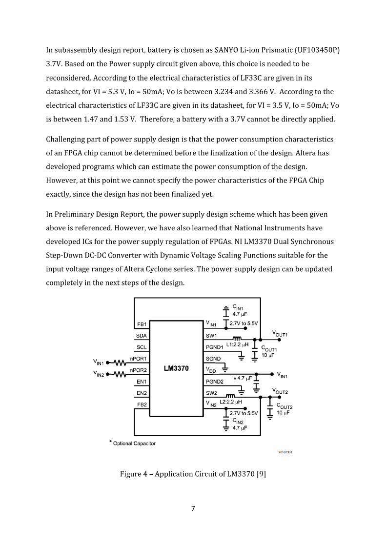
In subassembly design report, battery is chosen as SANYO Li-ion Prismatic (UF103450P)
3.7V. Based on the Power supply circuit given above, this choice is needed to be
reconsidered. According to the electrical characteristics of LF33C are given in its
datasheet, for VI = 5.3 V, Io = 50mA; Vo is between 3.234 and 3.366 V. According to the
electrical characteristics of LF33C are given in its datasheet, for VI = 3.5 V, Io = 50mA; Vo
is between 1.47 and 1.53 V. Therefore, a battery with a 3.7V cannot be directly applied.
Challenging part of power supply design is that the power consumption characteristics
of an FPGA chip cannot be determined before the finalization of the design. Altera has
developed programs which can estimate the power consumption of the design.
However, at this point we cannot specify the power characteristics of the FPGA Chip
exactly, since the design has not been finalized yet.
In Preliminary Design Report, the power supply design scheme which has been given
above is referenced. However, we have also learned that National Instruments have
developed ICs for the power supply regulation of FPGAs. NI LM3370 Dual Synchronous
Step-Down DC-DC Converter with Dynamic Voltage Scaling Functions suitable for the
input voltage ranges of Altera Cyclone series. The power supply design can be updated
completely in the next steps of the design.
Figure 4 – Application Circuit of LM3370 [9]

8
2. Technology Demonstration Test Plan
Hardware demonstration will have two main parts fist part will be establishing the
Bluetooth connection between computer and the Bluetooth device using Texas
Instruments’ CC2540 Mini Development Kit, second part will be the demonstration of
the decryption/encryption on D/E module, which will be the RSA public key encryption
implemented on Basys™2 Spartan-3E FPGA Board. Testing of the components will be
explained under Testing of the Prototype title.
3.1 Testing of the Prototype
For hardware part, we will test the Bluetooth connection and the D/E module which are
explained in detail as following:
3.1.1Testing the Bluetooth connection: We are using Texas Instruments’ CC2540 Mini
Development Kit, as we will use CC2540 Bluetooth chip in our original design. To test
the Bluetooth connection, we will connect the dongle (shown in Figure 2) to the
computer and establish a connection, between the computer and the Keyfob (Shown in
figure 5) which is the device that will be acting as the BLE Slave. Testing to see if the
Bluetooth connection is established or not will be carried out by pressing the buttons on
the keyfob and seeing the response on the computer. By the interview III, we will also
try to connect the Keyfob to the Basys 2 FPGA board, if we can do this, we will also show
the connection between the Bluetooth and FPGA modules.
3.1.2 Testing the D/E module: We are using Basys2 Spartan-3E FPGA Board from
Digilent Inc. (Shown in figure 6) to perform the encryption/decryption. Testing RSA
public key encryption implementation on FPGA will be very straightforward. We will
send a location data to FPGA boards input pins using the switches on the training board,
and after FPGA performs the encryption, it will show the encrypted data on its 7
segment display. To check whether the module operates correctly or not will be carried
out by a MATLAB code, which will also perform the same algorithm and return the
encrypted data for the same input as in the training board. The steps for checking
decryption on FPGA will be the same as encryption.

9
Figure 5 - Keyfob of TI’s CC2540 Mini Development Kit [8]
Figure 6: Basys™2 Spartan-3E FPGA Board

10
3. Conclusion 3.1 Current Position At the current stage, the project requirements and their technical corresponding
specifications are ready. In preliminary design report, top modules of the hardware
block have been defined. First version of the Development Plan will be finalized soon
accordingly. These documentations allowed us to see the whole picture. We have
divided into project two stages: development of VHDL Algorithms with communications
protocols and implementation of the design on the printed circuit board. It can be said
that mainly Power Supply SCC 001-004 and Bluetooth Module SCC 001-002 are related
with the implementation process. Their designs are not challenging. They are basically
taken from the related datasheets or reference papers. However, implementation
requires hard work. Design of FPGA Chip SCC 001-003 is the most important part of the
project. Its implementation is straightforward; however, configuring Altera chips still
require discussion. Details of the timeline will be given in the Development Plan.
3.2 Pitfalls & Risks
3.2.1 Insufficient RSA Key Length: The performance of the encryption has been
discussed extensively in the Preliminary Design Report and this report. 128-bit
RSA Encryption and Decryption is seen as the minimum requirement for the
success of this project. After this has been succeeded, HW Group started to
improve this algorithm in order to reach 1024-bit key lengths. However, as it has
been explained in the Preliminary Design Report, developments in the algorithm
may cause possible changes in the component choices. According to the
researches, EP1C3T100C8N will not be sufficient.
3.2.2 Changing FPGA Chip: As it has been summarized above, choice of FPGA Chip
may be changed due to algorithm developments. It is certain that a possible
change increases the cost of the product and cause update of the Business Plan.
Technically, FPGA Chip change requires the modification of the Power Supply
circuitry, since the power regulators are chosen according to the FPGA Chip
model. Two precautions can be considered to overcome the results of this risk:

11
Power supply circuitry is implemented with NI LM3370 Integrated Circuit and
other FPGA Chips are chosen again from ALTERA Cyclone family. NI LM3370 IC
power supply implementation is practical since it is compatible with the different
FPGA families [9]. ALTERA Cyclone FPGA Family Vcore and VI/O electrical
characteristics are same.
3.2.3 Battery Choice: Power supply issues are the pitfalls of FPGA Programming since
the power consumption characteristics are heavily dependent on the algorithm
implemented by the core. In the Subassembly Specifications Report, SANYO Li-
Ion Prismatic (UF103450P) battery has been chosen due to its high capacity
(2000mAh) as the safest choice to satisfy the technical specifications. This battery
will be altered since it is not compatible with the voltage input requirements of
the power supply circuitry. ALTERA’s PowerPlay early power estimator and the
Quartus II PowerPlay power analyzers are capable of estimating the power
consumption of the chip. However, these simulations can only be done after the
finalization of the algorithm. After the understanding of the power consumption
characteristics of the FPGA Chip, battery can be chosen more intelligently.
3.2.4 Configuration of the FPGA Chip: After the algorithm has been studied and
tested on Basys2 Development Kit, it is aimed to implement it on the industrial
Altera FPGA Chips. Configurations of the Altera Cyclone FPGAs are explained
extensively in the documentation of the producer [11]. This document offers
three different options and guides all steps in the implementation of these
configuration schemes. However, the critical point which is open to discussion is
that should HW group effort on the implementation of this configuration circuit
or try to obtain it from another source. In expenditure plan, HW group asked for a
serial configuration device Altera EPCS1 which is compatible with the Altera
Cyclone Series FPGAs in order to implement Active Serial Configuration scheme
drawn on Figure 7. This scheme is chosen since it has the simplest hardware
diagram. Other schemes require the usage of download cables which have very
high costs (more than 100 US Dollars). However, Hardware group is certainly
eager to obtain (or borrow) a readily prepared configuration scheme if it is
possible.

12
Figure 7 – Active Serial Configuration Scheme [11]
3.2.5 Bluetooth Module Application Circuit Implementation: As it can be seen on
Figure 1, TI CC2540 Bluetooth Module is connected to an external antenna with a
matching circuitry. Implementation of this Microwave frequency range
electronics component requires utmost care. It is expected that this would be a
great challenge if HW group tries to implement this circuitry by their own efforts.
It is certain that EE Engineers will advise the experts.
13
4. References [1] 2.4-GHz Bluetooth® low energy System-on-Chip Datasheet:
http://www.ti.com/lit/ds/swrs084c/swrs084c.pdf
[2] Small Size 2.4 GHz PCB antenna Application Note http://www.ti.com/lit/an/swra117d/swra117d.pdf [3]Antenna Selection Quick Guide http://www.ti.com/lit/an/swra351/swra351.pdf [4]Antenna Selection Guide Application Note AN058 http://www.ti.com/lit/an/swra161b/swra161b.pdf [5] “Three Reasons to Use FPGAs in Industrial Designs” Last Accessed on 18.11.2011 http://dkc1.digikey.com/us/en/tod/Altera/Reasons-To-Use-FPGAs_noaudio/Reasons-To-Use-FPGAs_noaudio.html [6] “FPGA Implementation of RSA Encryption Engine with Flexible Key Size” by Muhammad I. Ibrahimy, Mamun B.I. Reaz, Khandaker Asaduzzaman and Sazzad Hussain. [7] “Digi-Key Corporation” http://www.digikey.com/?curr=USD [8] “Design Guide for Altera FPGA Power Management Systems” http://www.digikey.com/Web%20Export/Supplier%20Content/STMicroelectronics_497/PDF/FPGA_Altera.pdf?redirected=1 [9] “LM3370 Dual Synchronous Step-Down DC-DC Converter with Dynamic Voltage Scaling Function” National Instruments Literature Number: SNVS406M [10]CC2540 Mini Development Kit http://www.ti.com/tool/cc2540dk-mini [11] “Configuring Cyclone FPGAs” ALTERA March 2003, ver1.1 Application Note 250