chunghwa picture tubes, ltd. technical · pdf filechunghwa picture tubes, ltd. technical...
TRANSCRIPT

CChhuunngghhwwaa PPiiccttuurree TTuubbeess,, LLttdd.. TTeecchhnniiccaall SSppeecciiffiiccaattiioonn
To : Date : 2009/05/04
CPT TFT-LCD CLAA 185WA 03
APPROVED BY CHECKED BY PREPARED BY
Product Planning
Management General Division
ACCEPTED BY:
CHUNGHWA PICTUER TUBES, LTD.
No. 1, Huaying Rd., Sanho Tsun, Lungtan Shiang, Taoyuan, Taiwan, 325, R.O.C. TEL: +886-3-4805678 FAX: +886-3-4800589
Doc. No: CLAA185WA03-SPEC-Ver.1-20090504 Issue Date: 2009/05/04
www.yslcd.com.tw
Studio
Technolo
gy Co.,
Ltd

CPT CHUNGHWA PICTURES TUBES, LTD.,
CPT Confidential 2/22 CLAA185WA03-SPEC-Ver.1-20090504
ʳ ʳ ʳ ʳ ʳ ʳ ʳ ʳ ʳ ʳ ʳ ʳ ʳ ʳ
1. OVERVIEW CLAA185WA03 is 18.51” color TFT-LCD (Thin Film Transistor Liquid Crystal Display) module composed of LCD panel, driver ICs, control circuit and backlight. By applying 6bit+Hi-FRC digital data, 1366*768, 16.7M-color images are displayed on the 18.51” diagonal screen. Input power voltage is 5.0V for LCD driving. Inverter for backlight is not included in this module. General specification are summarized in the following table:
ITEM SPECIFICATION Display Area(mm) 409.8(H)x230.4(V) Number of Pixels 1366(H)x768(V) Pixel Pitch(mm) 0.3(H)x0.3 (V) Color Pixel Arrangement RGB vertical stripe Display Mode normally white, TN Number of Colors 16.7M(6 Bit+Hi-FRC) Brightness(cd/m^2) 250 cd/m2(Typ.) (Center point, Lamp current=7.5 mA) Viewing Angle 170 / 160 Surface Treatment Anti-glare, Hard coating(3H) Power consumption(W) 14.5(typ) Module Size(mm) 430.37(W)x254.6(H)x16.5(D) Module Weight(g) 2000(typ) Backlight Unit CCFL, 2 tables, edge-light(top*1/bottom*1)
www.yslcd.com.tw
Studio
Technolo
gy Co.,
Ltd

CPT CHUNGHWA PICTURES TUBES, LTD.,
CPT Confidential 3/22 CLAA185WA03-SPEC-Ver.1-20090504
2. ABSOLUTE MAXIMUM RATINGS
ITEM SYMBOL MIN. MAX. UNIT REMARKPower Supply Voltage for LCD VCC 0 6 V
Lamp Voltage VL 620 830 Vrms
Lamp Current ILO 3 8 mArms *4). 7) Lamp Frequency FL 40 80 kHz
VESDt -200 200 V static electricity VESDc -8000 8000 V *5)
Operation Temperature Top 0 50 к *1). 2). 3). 6)Storage Temperature Tstg -20 60 к *1). 2). 3)
Delayed Discharge Time TD -- 1 sec *8) [Note]
1).The relative temperature and humidity range are as below sketch, 90%RHMax.(TaЉ40к). 2).The maximum wet bulb temperature 39 (TaЉ к Ї40 ) and without dewinк g. 3).If you use the product in a environment which over the definition of temperature and humidity
too long to effect the result of eye-aching. 4).The life time of the lamp is related to the current of the lamp, so please according to the
description of the “(b) backlight” on page 7. 5).Test Condition: IEC 1000-4-2
VESDt: Contact discharge to input connector; VESDC: Contact discharge to module 6).If you operate the product in normal temperature range, the center surface of panel should be
under 60к. 7).When lamp current is out of the absolute maximum range, the life will fall rapidly or shown
unusual sign. IL min 2mA only for test only, but we can’t guarantee the lifetime and performance.
8).Delay lighting testing needs the volt above start voltage Vrms. Before the procedure tube needs typical lighting for 1 minute and stay in the temperature 25±2к for 24 hours and then testing in the same condition in dark room.
ʳ ʳ ʳ ʳ ʳ ʳ ʳ ʳ ʳ ʳ ʳ ʳ ʳ ʳ www.yslcd.com.tw
Studio
Technolo
gy Co.,
Ltd

CPT CHUNGHWA PICTURES TUBES, LTD.,
CPT Confidential 4/22 CLAA185WA03-SPEC-Ver.1-20090504
3. ELECTRICAL CHARACTERISTICS
(1).TFT-LCD Ta=25к
ITEM SYMBOL MIN TYP MAX UNIT RemarkPower Supply Voltage for LCD Vcc 4.5 5.0 5.5 V *1) Power Supply Current for LCD Icc - 700 1000 mA *2) Permissive Input Ripple Voltage VRP - - 100 mVp-p Vcc=5.0VDifferential impedance Zm 90 100 110 ȍ
Common Mode Voltag VCM 1.125 1.25 1.375 V
Differential Input Voltage |VID| 250 350 450 mV
Threshold Voltage(High) VTH - - 100 mV
Logic input voltage LVDS:IN+ΔIN-
Threshold Voltage(Low) VTL -100 - - mV
*3)
LCD Inrush Current Inrush 3 A *4) Power consumption P 3.5 5.5 W *2)
[Note] 1).VCC-turn-on conditions:
0.5msЉt1Љ10ms 1 secЉt4 0Іt2Љ20ms 200msЉt5
0Іt3Љ50ms 200msЉt6
data
t1 t2 t3
4.5V4.5V
0.5V
Vin=5.0V
0.5V 0.5V
t4
LCD Power Supply
Logic Signal
t5 t6
Backlight Power Supply
VL
Data: RGB DATA, DCLK, DENA
ʳ ʳ ʳ ʳ ʳ ʳ ʳ ʳ ʳ ʳ ʳ ʳ ʳ ʳ www.yslcd.com.tw
Studio
Technolo
gy Co.,
Ltd

CPT CHUNGHWA PICTURES TUBES, LTD.,
CPT Confidential 5/22 CLAA185WA03-SPEC-Ver.1-20090504
VCC-dip conditions: (1) When 3.6VЉVcc(min)<4.5V: tdЉ10 ms (2) When Vcc <3.6 V, VCC-dip conditions should also follow the VCC-turn-on conditions.
2).Typical current situation: 256 gray scale level, VCC=5.0V, Fh=47.28KHz, Fv=60Hz, Fclk=67.1 MHz.
ʳ ʳ ˠ˴ʳ˶˸ʳ˼˴˼ˍʳ˖˦ʳˢ˸ʳ˶˴˿˸ʳ˿˸˸˿ʿʳ˩˖˖ːˈˁ˃˩ʿʳ˙˻ːˇˊˁ˅ˋ˞˛ʿʳ˙ːˉ˃˛ʿʳ˙˶˿˾ːˉˊˁ˄ʳ
ˠ˛ˁʳ
3).LVDS Signal definition:
VID = VIN+ – VIN- , VIN+ = Positive differential DATA & CLK Input
VIN- = Negative differential DATA & CLK InputϦVCM =ΨVCM+–VCM-Ψ, ϦVID =ΨVID+–VID-Ψ, VID+ =ΨVIH+–VIH-Ψ, VID- =ΨVIL+–VIL-Ψ, VCM =(VIN+ +VIN-)/2, VCM+ =(VIH+ +VIH-)/2, VCM- =(VIL+ +VIL-)/2,
4).Irush Measurement Condition
ʳ ʳ ʳ ʳ ʳ ʳ ʳ ʳ ʳ ʳ ʳ ʳ ʳ ʳ www.yslcd.com.tw
Studio
Technolo
gy Co.,
Ltd

CPT CHUNGHWA PICTURES TUBES, LTD.,
CPT Confidential 6/22 CLAA185WA03-SPEC-Ver.1-20090504
(2).Backlight 1. Electrical specification
ITEM SYMBOL MIN TYP MAX UNIT REMARK
B/L Voltage VL 657 740 803 Vrms IL=7.5mA Ta=25к
B/L Current IL 7 7.5 8 mArms *1) *3) Ta=25к B/L operating current ILO 3 7.5 8 mArms *1) *3 )Ta=25к
B/L power consumption WL Ё 11 Ё W IL=7.5mA Ta=25к
Inverter Frequency FI 40 50 60 kHz *2) Ta=25к Ё Ё 1700 Vrms *9)Ta=0к
Starting Lamp Voltage VS Ё Ё 1400 Vrms *9)Ta=25к
PWM Dimming Ratio Ё 20 - 100 % *4)
2. Lamp life time ITEM ILO at 3.0 mA ILO at 7.5 mA ILO at 8.0 mA UNIT REMARK
Lamp life Time Min. 50,000 Min. 40,000 Min. 30,000 hr Continuous Operation *3)
Rated time (turn on/off) Ё Min. 10,000 Ё time *4)
ʳ ʳ ʳ ʳ ʳ ʳ ʳ ʳ ʳ ʳ ʳ ʳ ʳ ʳ www.yslcd.com.tw
Studio
Technolo
gy Co.,
Ltd
CPT CHUNGHWA PICTURES TUBES, LTD.,
CPT Confidential 7/22 CLAA185WA03-SPEC-Ver.1-20090504
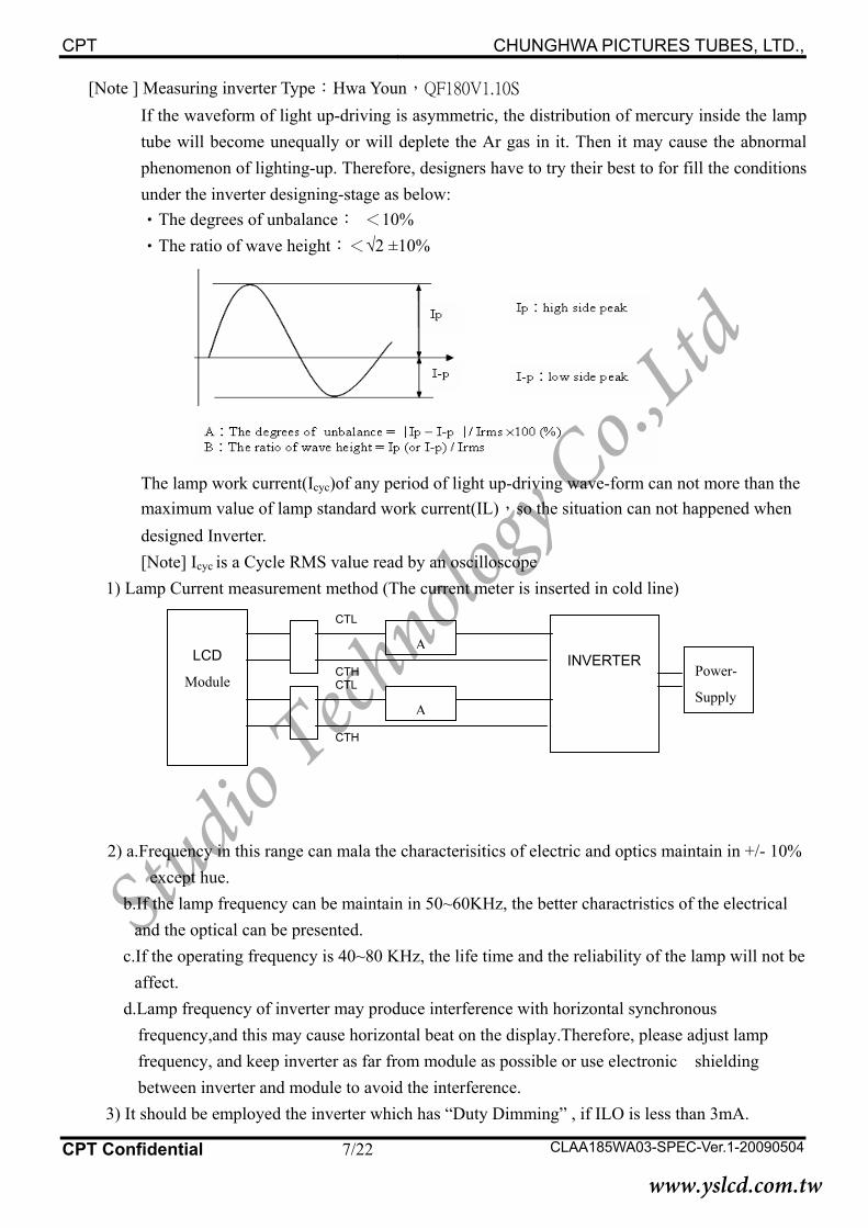
[Note ] Measuring inverter TypeΚHwa YounΔˤ˙˄ˋ˃˩˄ˁ˄˃˦ If the waveform of light up-driving is asymmetric, the distribution of mercury inside the lamp tube will become unequally or will deplete the Ar gas in it. Then it may cause the abnormal phenomenon of lighting-up. Therefore, designers have to try their best to for fill the conditions under the inverter designing-stage as below: ΘThe degrees of unbalanceΚ І10% ΘThe ratio of wave heightΚІ¥2 ±10%
The lamp work current(Icyc)of any period of light up-driving wave-form can not more than the maximum value of lamp standard work current(IL)Ǵso the situation can not happened when designed Inverter. [Note] Icyc is a Cycle RMS value read by an oscilloscope
1) Lamp Current measurement method (The current meter is inserted in cold line)
CTH
CTH
CTL
A
CTL
A
Power-
Supply
INVERTER
LCD
Module
2) a.Frequency in this range can mala the characterisitics of electric and optics maintain in +/- 10% except hue.
b.If the lamp frequency can be maintain in 50~60KHz, the better charactristics of the electrical and the optical can be presented.
c.If the operating frequency is 40~80 KHz, the life time and the reliability of the lamp will not be affect.
d.Lamp frequency of inverter may produce interference with horizontal synchronous frequency,and this may cause horizontal beat on the display.Therefore, please adjust lamp frequency, and keep inverter as far from module as possible or use electronic shielding between inverter and module to avoid the interference.
3) It should be employed the inverter which has “Duty Dimming” , if ILO is less than 3mA.
ʳ ʳ ʳ ʳ ʳ ʳ ʳ ʳ ʳ ʳ ʳ ʳ ʳ ʳ www.yslcd.com.tw
Studio
Technolo
gy Co.,
Ltd

CPT CHUNGHWA PICTURES TUBES, LTD.,
CPT Confidential 8/22 CLAA185WA03-SPEC-Ver.1-20090504
ʳ ʳ ʳ ʳ ʳ ʳ ʳ ʳ ʳ ʳ ʳ ʳ ʳ ʳ
4) The CCFL can work normally if the PWM Dimming Ratio range is from 20% to 100% and the lamp current is 7.5mA.
5) Definition of the lamp life timeΚ Luminance (L) under 50% of specification starting lamp voltage or starting lamp voltage is more than 130% of the initial value
6) The condition of Turn-on and Turn-off operation is as below: a. Lamp current is 7.5mA b. Frequency is 30 sec. (on)/30 sec. (off) c. Repeat it for 10 thousand times d. The result of eye-aching of the lamp hue is normal, and can switch the lamp.
It should not have motion fail when starting lamp voltage is lower than 130% of the initial value.
7) It is necessary to consider the maximal value when design inverterΔin order to assure lighting. 8) The equation of power consumption WL=IL x VL x 2.(IL=7.5mAΔTa=25к) 9) The voltage above VS should be applied to the lamps for more than 1 second for start-up.
(Inverter open voltage must be more than lamp starting voltage.)
www.yslcd.com.tw
Studio
Technolo
gy Co.,
Ltd

CPT CHUNGHWA PICTURES TUBES, LTD.,
CPT Confidential 9/22 CLAA185WA03-SPEC-Ver.1-20090504
ʳ ʳ ʳ ʳ ʳ ʳ ʳ ʳ ʳ ʳ ʳ ʳ ʳ ʳ
4. INTERFACE PIN CONNECTION
(1) CN1 (Data Signal and Power Supply) Used connector: 093G30-B2001A (STARCONN) or compatible.
PIN NO. SYMOBL FUNCTION ˄ʳ NC NC ˅ʳ NC NC ˆʳ NC NC ˇʳ GND Power ground ˈʳ RXIN0- Negative LVDS differential data input(0) ˉʳ RXIN0+ Positive LVDS differential data input(0) ˊʳ GND Power ground ˋʳ RXIN1- Negative LVDS differential data input(1) ˌʳ RXIN1+ Positive LVDS differential data input(1) ˄˃ʳ GND Power ground ˄˄ʳ RXIN2- Negative LVDS differential data input(2) ˄˅ʳ RXIN2+ Positive LVDS differential data input(2) ˄ˆʳ GND Power ground ˄ˇʳ RXCLKIN- Negative LVDS differential clock input(clock) ˄ˈʳ RXCLKIN+ Positive LVDS differential clock input(clock) ˄ˉʳ GND Power ground ˄ˊʳ RXIN3- Negative LVDS differential data input(3) ˄ˋʳ RXIN3+ Positive LVDS differential data input(3) ˄ˌʳ GND Power ground ˅˃ʳ NC NC ˅˄ʳ NC NC ˅˅ʳ NC NC ˅ˆʳ GND Power ground ˅ˇʳ GND Power ground ˅ˈʳ GND Power ground ˅ˉʳ VCC Power supply input voltage(5.0 V) ˅ˊʳ VCC Power supply input voltage(5.0 V) ˅ˋʳ VCC Power supply input voltage(5.0 V) ˅ˌʳ VCC Power supply input voltage(5.0 V) ˆ˃ʳ VCC Power supply input voltage(5.0 V)
(2) CN2, 3 (BACKLIGHT)
Backlight-side connector: CP0502SL090 )CVILUX) or compatible!xInverter-side connector: CP0502P1ML0-LF )CVILUX) or compatible!
Pin No. Symbol Function 1 CTH Power for CCFL 2 CTL Power return for CCFL
www.yslcd.com.tw
Studio
Technolo
gy Co.,
Ltd

CPT CHUNGHWA PICTURES TUBES, LTD.,
CPT Confidential 10/22 CLAA185WA03-SPEC-Ver.1-20090504
5. INTERFACE TIMING
(1) Timing Specifications ITEM SYMBOL MIN TYP MAX UNIT Frequency fCLK ˈˇˁˈʳ ˉˊˁ˄ʳ ˋˌˁ˃ʳ MHz DCLK Period tCLK ˄ˋˁˇʳ ˄ˇˁˌʳ ˄˄ˁˌʳ ns Horizontal Active Time tHA ˄ˆˉˉʳ ˄ˆˉˉʳ ˄ˆˉˉʳ tCLK
Horizontal Blank Time tHB ˆˇʳ ˈˇʳ ˊˇʳ tCLK
Horizontal Total Time tH ˄ˇ˃ˉʳ ˄ˇ˅˃ʳ ˄ˇˉ˃ʳ tCLK
Vertical Active Time tVA ˊˉˋʳ ˊˉˋʳ ˊˉˋʳ tH
Vertical Blank Time tVB ˋʳ ˅˃ʳ ˆ˅ʳ tH
Vertical Total Time tV ˊˊˉʳ ˊˋˋʳ ˋ˅˃ʳ tH
LCD Timing
DENA
Vertical Frame Rate Hz Fr ˈ˃ʳ ˉ˃ʳ ˊˈʳ
[Note] 1) DENA should always be positive polarity as shown in the timing specification. 2) CLK INshould appear during all blanking period,
(2) Timing Chart
a. Horizontal Timing
(R, G, B) tHB
Invalid Data
EDML
First Data
2 3!EBUB!
1 1365 1366 Invalid Data
Last Data
tHAEFOA
tCLK
b. Vertical Timing
DENA
tVA
LINE DATA Invalid Data
Invalid Data 1 2 767 768 3
tV
ʳ ʳ ʳ ʳ ʳ ʳ ʳ ʳ ʳ ʳ ʳ ʳ ʳ ʳ www.yslcd.com.tw
Studio
Technolo
gy Co.,
Ltd

CPT CHUNGHWA PICTURES TUBES, LTD.,
CPT Confidential 11/22 CLAA185WA03-SPEC-Ver.1-20090504
(3) LVDS DATA (a) Timing Chart
RXIN0
RXIN1
RXIN2
RXIN3
(b) Data mapping
*)ΚDS90C383MTD
ʳ ʳ ʳ ʳ ʳ ʳ ʳ ʳ ʳ ʳ ʳ ʳ ʳ ʳ www.yslcd.com.tw
Studio
Technolo
gy Co.,
Ltd

CPT CHUNGHWA PICTURES TUBES, LTD.,
CPT Confidential 12/22 CLAA185WA03-SPEC-Ver.1-20090504
ʳ ʳ ʳ ʳ ʳ ʳ ʳ ʳ ʳ ʳ ʳ ʳ ʳ ʳ
(4) Color Data Assignment R DATA G DATA B DATA
R7 R6 R5 R4 R3 R2 R1 R0 G7 G6 G5 G4 G3 G2 G1 G0 B7 B6 B5 B4 B3 B2 B1 B0COLOR INPUT DATA MSB LSB MSB LSB MSB LSB
BLACK 0 0 0 0 0 0 0 0 0 0 0 0 0 0 0 0 0 0 0 0 0 0 0 0RED(255) 1 1 1 1 1 1 1 1 0 0 0 0 0 0 0 0 0 0 0 0 0 0 0 0GREEN(255) 0 0 0 0 0 0 0 0 1 1 1 1 1 1 1 1 0 0 0 0 0 0 0 0BLUE(255) 0 0 0 0 0 0 0 0 0 0 0 0 0 0 0 0 1 1 1 1 1 1 1 1CYAN 0 0 0 0 0 0 0 0 1 1 1 1 1 1 1 1 1 1 1 1 1 1 1 1MAGENTA 1 1 1 1 1 1 1 1 0 0 0 0 0 0 0 0 1 1 1 1 1 1 1 1YELLOW 1 1 1 1 1 1 1 1 1 1 1 1 1 1 1 1 0 0 0 0 0 0 0 0
BASIC COLOR
WHITE 1 1 1 1 1 1 1 1 1 1 1 1 1 1 1 1 1 1 1 1 1 1 1 1RED(0) 0 0 0 0 0 0 0 0 0 0 0 0 0 0 0 0 0 0 0 0 0 0 0 0
RED(1) 0 0 0 0 0 0 0 1 0 0 0 0 0 0 0 0 0 0 0 0 0 0 0 0RED(2) 0 0 0 0 0 0 1 0 0 0 0 0 0 0 0 0 0 0 0 0 0 0 0 0 RED(254) 1 1 1 1 1 1 1 0 0 0 0 0 0 0 0 0 0 0 0 0 0 0 0 0
RED
RED(255) 1 1 1 1 1 1 1 1 0 0 0 0 0 0 0 0 0 0 0 0 0 0 0 0GREEN(0) 0 0 0 0 0 0 0 0 0 0 0 0 0 0 0 0 0 0 0 0 0 0 0 0
GREEN(1) 0 0 0 0 0 0 0 0 0 0 0 0 0 0 0 1 0 0 0 0 0 0 0 0GREEN(2) 0 0 0 0 0 0 0 0 0 0 0 0 0 0 1 0 0 0 0 0 0 0 0 0 GREEN(254) 0 0 0 0 0 0 0 0 1 1 1 1 1 1 1 0 0 0 0 0 0 0 0 0
GREEN
GREEN(255) 0 0 0 0 0 0 0 0 1 1 1 1 1 1 1 1 0 0 0 0 0 0 0 0BLUE(0) 0 0 0 0 0 0 0 0 0 0 0 0 0 0 0 0 0 0 0 0 0 0 0 0
BLUE(1) 0 0 0 0 0 0 0 0 0 0 0 0 0 0 0 0 0 0 0 0 0 0 0 1BLUE(2) 0 0 0 0 0 0 0 0 0 0 0 0 0 0 0 0 0 0 0 0 0 0 1 0 BLUE(254) 0 0 0 0 0 0 0 0 0 0 0 0 0 0 0 0 1 1 1 1 1 1 1 0
BLUE
BLUE(255) 0 0 0 0 0 0 0 0 0 0 0 0 0 0 0 0 1 1 1 1 1 1 1 1
[Note] 1) Definition of gray scale: Color (n): n indicates gray scale level. Higher n means brighter level. 2) Data: 1-High, 0-Low. 3) This assignment is applied to both odd and even data.
(5) Color Data Assignment
D(1,1) D(2,1) -- D(X,1) -- D(1365,1) D(1366,1) D(1,2) D(2,2) -- D(X,2) -- D(1365,2) D(1366,2)
| | + .. + | |
D(1,Y) D(2,Y) -- D(X,Y) -- D(1365,Y) D(1366,Y)
| | + .. + | |
D(1,767) D(2, 767) -- D(X, 767) -- D(1365,767) D(1366,767)
D(1,768) D(2, 768) -- D(X, 768) -- D(1365,768) D(1366,768)
www.yslcd.com.tw
Studio
Technolo
gy Co.,
Ltd

CPT CHUNGHWA PICTURES TUBES, LTD.,
CPT Confidential 13/22 CLAA185WA03-SPEC-Ver.1-20090504
6. BLOCK DIAGRAM
LVDS receiver 1ch
Timing Controller
Lamp Unit in Backlight
Source Driver
LCD Panel
1366 X 3 X 768 Gat
e D
river
Power Supply Circuit
CN2
TFT-LCD Module
Lamp Uint in Backlight
CCFL
1
2
CN2
CN
1 I/F
Con
nect
or
CN3Lamp Unit in Backlight
1
2
CN3
CCFL
ʳ ʳ ʳ ʳ ʳ ʳ ʳ ʳ ʳ ʳ ʳ ʳ ʳ ʳ www.yslcd.com.tw
Studio
Technolo
gy Co.,
Ltd

CPT CHUNGHWA PICTURES TUBES, LTD.,
CPT Confidential 14/22 CLAA185WA03-SPEC-Ver.1-20090504
7. MECHANICAL SPECIFICATION
(1) Front side (Tolerance is ±0.5mm unless noted) Unit: mm
ʳ ʳ ʳ ʳ ʳ ʳ ʳ ʳ ʳ ʳ ʳ ʳ ʳ ʳ www.yslcd.com.tw
Studio
Technolo
gy Co.,
Ltd

CPT CHUNGHWA PICTURES TUBES, LTD.,
CPT Confidential 15/22 CLAA185WA03-SPEC-Ver.1-20090504
(2) Rear side (Tolerance is ±0.5mm unless noted) Unit: mm
ʳ ʳ ʳ ʳ ʳ ʳ ʳ ʳ ʳ ʳ ʳ ʳ ʳ ʳ www.yslcd.com.tw
Studio
Technolo
gy Co.,
Ltd

CPT CHUNGHWA PICTURES TUBES, LTD.,
CPT Confidential 16/22 CLAA185WA03-SPEC-Ver.1-20090504
8. OPTICAL CHARACTERISTICS Ta=25кΔVCC=5.0V
ITEM SYMBOL CONDITION min typ max UNIT REMARK
T=ȥГ0° Contrast Ratio CR 700 1000 -- -- *1) 2)
ʳ ʳ ʳ ʳ ʳ ʳ ʳ ʳ ʳ ʳ ʳ ʳ ʳ ʳ
Luminance(CEN) L T=ȥГ0° 200 250 -- cd/m2 *1) 3) 9P Uniformity 75 -- -- *1) 3) T=ȥГ0° 'L �
T=ȥГ0° Tr -- ms Response Time 5 8 *5)
T=ȥГ0° Tf -- ms -- Crosstalk CT 0 1 % *6) T=ȥГ0°
Horizontal Ȍ(L/R) *4) 150 170 -- Viewing Angle CR 10Њ *3)
Vertical T(U/D) 140 160 -- X 0.283 0.313 0.343 White Y 0.299 0.329 0.359 X 0.620 0.650 0.680 Red Y 0.305 0.335 0.365
Green X Y
0.252 0.586
0.282 0.616
0.312 0.646
Color Coordinates T=ȥГ0° *3) *2)
X 0.116 0.146 0.176 Blue Y 0.055 0.085 0.115
Gamma Ȗ VESA 2.0 2.2 2.4 -- *7) [Note]
1)All optical specification condition: (1) Equipment: Color coordinate and color gamut are measured by CS-1000, and all the other items
are measured by BM-5A (TOPCON). (2) Condition: IL=7.5 (each lamp) mA, Inverter: Hwa YounΔˤ˙˄ˋ˃˩˄ˁ˄˃˦, Frequency=50 kHz. (3)The LCD module should be turn-on to a stable luminance level to be reached. The measurement
should be executed after lighting Backlight for 20 minutes and in a dark room.
2).Definition of Contrast Ratio: CR=ON (White) Luminance/OFF (Black) Luminance
www.yslcd.com.tw
Studio
Technolo
gy Co.,
Ltd

CPT CHUNGHWA PICTURES TUBES, LTD.,
CPT Confidential 17/22 CLAA185WA03-SPEC-Ver.1-20090504
3).Definition of Luminance and Luminance uniformity: Center Luminance: measuring the luminance of the point no. 5 Average Luminance: measuring average luminance of points no.1-no.9
Uniformity: ǻL= [L (Min)/L (Max)] ×100 %
4).Definition of Viewing Angle (ș,ȥ):
ӽUpper
Right
Lower
Left
Ӱ
5) Definition of Response Time:
Luminan
White
Black
90 % 90 %
10 % 10 % tf tr
ʳ ʳ ʳ ʳ ʳ ʳ ʳ ʳ ʳ ʳ ʳ ʳ ʳ ʳ www.yslcd.com.tw
Studio
Technolo
gy Co.,
Ltd

CPT CHUNGHWA PICTURES TUBES, LTD.,
CPT Confidential 18/22 CLAA185WA03-SPEC-Ver.1-20090504
6) Definition of crosstalk: 6) Definition of crosstalk: CT= YЮ -Y
ʳ ʳ ʳ ʳ ʳ ʳ ʳ ʳ ʳ ʳ ʳ ʳ ʳ ʳ
ʳːӫˀ˾
ᔕ
৫
L
O
ၸᓳLOG Gray level (LOG)
T%
B A /YЮ A X 100 (%) CT= YЮ -YYA: The luminance of measured position at pattern A YYB: The luminance of measured position at pattern B with Gray level 0 Y
B A /YЮ A X 100 (%) A: The luminance of measured position at pattern A B: The luminance of measured position at pattern B with Gray level 0
Pattern A Pattern B 7) Definition of Gamma (Ȗ), follow VESA standard sampling every 16 gray level (0, 16, 32,…..224,240,255)
www.yslcd.com.tw
Studio
Technolo
gy Co.,
Ltd

CPT CHUNGHWA PICTURES TUBES, LTD.,
CPT Confidential 19/22 CLAA185WA03-SPEC-Ver.1-20090504
9. RELIABILITY TEST CONDITIONS
(1) Temperature and Humidity TEST ITEMS CONDITIONS
HIGH TEMPERATURE 50 ; 90%RH; 240hк HIGH HUMIDITY OPERATION (No condensation) HIGH TEMPERATURE 60 ; 90%RH;48hк HIGH HUMIDITY STORAGE (No condensation) HIGH TEMPERATURE OPERATION 50 ; 240hк HIGH TEMPERATURE STORAGE 60 ; 240hк LOW TEMPERATURE OPERATION 0 ; 240hк LOW TEMPERATURE STORAGE -20 ; 240hк
BETWEEN -20 (1hr)AND 60 (1hr); 100 к кCYCLES THERMAL SHOCK
(2) Shock & Vibration
ITEMS CONDITIONS Shock level:1470m/s^2(150G) SHOCK Waveform: half sinusoidal wave, 2ms (NON-OPERATIO
N) Number of shocks: 1/2 shock input in each direction of three mutually perpendicular axes for a total of six shock inputs Vibration level: 9.8m/s^2(1.0G) zero to peak Waveform: sinusoidal VIBRATION Frequency range: 5 to 500 Hz (NON-OPERATIO
N) Frequency sweep rate: 0.5 octave/min Duration: one sweep from 5 to 500Hz in each of three mutually perpendicular axis(each x,y,z axis: 1 hour, total 3 hours)
(3) ESD
POSITION CONDITION( MDL turn off) 1. 200 pFΔ0 ȍΔ±250 V Connector 2. contact mode for each pin 1. 150 pFΔ330 ȍΔ±15K V
Module 2. Air mode, test 25 times for each test point 3. Contact mode, 25 times for each test point
(4) Low Pressure test
TEST ITEM CONDITION 260HPa (30000 ft.)Ι24 Hr Low Pressure test(storage)
(5) Judgment standard
The judgment of the above test should be made as follow: Pass: Normal display image with no obvious non-uniformity and no line defect. Partial
transformation of the module parts should be ignored. Fail: No display image, obvious non-uniformity, or line defects.
ʳ ʳ ʳ ʳ ʳ ʳ ʳ ʳ ʳ ʳ ʳ ʳ ʳ ʳ www.yslcd.com.tw
Studio
Technolo
gy Co.,
Ltd

CPT CHUNGHWA PICTURES TUBES, LTD.,
CPT Confidential 20/22 CLAA185WA03-SPEC-Ver.1-20090504
ʳ ʳ ʳ ʳ ʳ ʳ ʳ ʳ ʳ ʳ ʳ ʳ ʳ ʳ
10. HANDLING PRECAUTIONS FOR TFT-LCD MODULE
Please pay attention to the followings in handling- TFT-LCD products; (1) ASSEMBLY PRECAUTION
1) Please use the mounting hole on the module side in installing and do not beading or wrenching LCD in assembling. And please do not drop, bend or twist LCD module in handling.
2) Please design display housing in accordance with the following guide lines. a) Housing case must be destined carefully so as not to put stresses on LCD all sides and not to
wrench module. The stresses may cause non-uniformity even if there is no non-uniformity statically.
b) Keep sufficient clearance between LCD module back surface and housing when the LCD module is mounted. Approximately 1.0 mm of the clearance in the design is recommended taking into account the tolerance of LCD module thickness and mounting structure height on the housing.
c) When some parts, such as, FPC cable and ferrite plate, are installed underneath the LCD module, still sufficient clearance is required, such as 0.5mm. This clearance is, especially, to be reconsidered when the additional parts are implemented for EMI countermeasure.
d) Design the inverter location and connector position carefully so as not to give stress to lamp cable, or not to interface the LCD module by the lamp cable.
e) Keep sufficient clearance between LCD module and the others parts, such as inverter and speaker so as not to interface the LCD module. Approximately 1.0mm of the clearance in the design is recommended.
3) Please do not push or scratch LCD panel surface with any-thing hard. And do not soil LCD panel surface by touching with bare hands. (Polarizer film, surface of LCD panel is easy to be flawed.)
4) Please do not press any parts on the rear side such as source TCP, gate TCP, control circuit board and FPCs during handling LCD module. If pressing rear part is unavoidable, handle the LCD module with care not to damage them.
5) Please wipe out LCD panel surface with absorbent cotton or soft cloth in case of it being soiled. 6) Please wipe out drops of adhesives like saliva and water on LCD panel surface immediately.
They might damage to cause panel surface variation and color change. 7) Please do not take a LCD module to pieces and reconstruct it. Resolving and reconstructing
modules may cause them not to work well. 8) Please do not touch metal frames with bare hands and soiled gloves. A color change of the
metal frames can happen during a long preservation of soiled LCD modules. 9) Please pay attention to handling lead wire of backlight so that it is not tugged in connecting wit
inverter. (2) OPERATING PRECAUTIONS
1) Please be sure to turn off the power supply before connecting and disconnecting signal input cable.
2) Please do not change variable resistance settings in LCD module. They are adjusted to the
www.yslcd.com.tw
Studio
Technolo
gy Co.,
Ltd

CPT CHUNGHWA PICTURES TUBES, LTD.,
CPT Confidential 21/22 CLAA185WA03-SPEC-Ver.1-20090504
ʳ ʳ ʳ ʳ ʳ ʳ ʳ ʳ ʳ ʳ ʳ ʳ ʳ ʳ
most suitable value. If they are changed, it might happen LCD does not satisfy the characteristics specification.
3) Please consider that LCD backlight takes longer time to become stable of radiation characteristics in low temperature than in room temperature.
4) A condensation might happen on the surface and inside of LCD module in case of sudden charge of ambient temperature.
5) Please pay attention to displaying the same pattern for very long time. Image might stick on LCD. If then, time going on can make LCD work well.
6) Please obey the same caution descriptions as ones that need to pay attention to ordinary electronic parts.
(3) PRECAUTFONSWITHELECTROSTATICS 1) This LCD module use CMOS-IC on circuit board and TFT-LCD panel, and so it is easy to be
affected by electrostatics. Please be careful with electrostatics by the way of your body connecting to the ground and so on.
2) Please remove protection film very slowly on the surface of LCD module to prevent from electrostatics occurrence.
(4) STORAGE PRECAUTIONS 1) When you store LCDs for a long time, it is recommended to keep the temperature between
0 ~40 without the exposure of sunlight and to keep the humidity less than 90%RH.к к 2) Please do not leave the LCDs in the environment of high humidity and high temperature such as
60 90%RH.к 3) Please do not leave the LCDs in the environment of low temperature; below -20к.
(5) SAFETY PRECAUTIONS 1) When you waste LCDS, it is recommended to crush damaged or unnecessary LCDs into pieces
and wash them off with solvents such as acetone and ethanol, which should later be burned. 2) If any liquid leaks out of a damaged-glass cell and comes in contact with the hands, wash off
thoroughly with soap and water. (6) OTHERS
1) A strong incident light into LCD panel might cause display characteristics' changing inferior because of polarizer film, color filter, and other materials becoming inferior. Please do not expose LCD module direct sunlight Land strong UV rays.
2) Please pay attention to a panel side of LCD module not to contact with other materials in preserving it alone.
3) For the. Packaging box, please pay attention to the followings: a) Packaging box and inner case for LCD are designed to protect the LCDs from the damage or
scratching during transportation. Please do not open except picking LCDs up from the box. b) Please do not pile them up more than 5 boxes. (They are not designed so.) And please do not
turn over. c) Please handle packaging box with care not to give them sudden shock and vibrations. And
www.yslcd.com.tw
Studio
Technolo
gy Co.,
Ltd

CPT CHUNGHWA PICTURES TUBES, LTD.,
CPT Confidential 22/22 CLAA185WA03-SPEC-Ver.1-20090504
also please do not throw them up. d) Packing box and inner case for LCDs are made of cardboard. So please pay attention not to get them wet. (Such like keeping them in high humidity or wet place can occur getting them wet.)
ʳ ʳ ʳ ʳ ʳ ʳ ʳ ʳ ʳ ʳ ʳ ʳ ʳ ʳ www.yslcd.com.tw
Studio
Technolo
gy Co.,
Ltd