ci40 hardware user guide - docs | creator · pdf fileit is not recommended to power the board...
TRANSCRIPT

Public Imagination Technologies
Ci40 1 Revision 3.2.132
Ci40
Hardware User Guide
Copyright © Imagination Technologies Limited. All Rights Reserved.
We make no warranty, representation, or guarantee regarding the information contained herein or on our website or the suitability of our products and services for any particular purpose. We make no
warranty that the Ci40 will be of a particular standard of quality, fit for a particular purpose or be free of any errors, bugs or mistakes. Nor do we assume any liability whatsoever (to the extent permitted by
law) arising out of the application or use of the Ci40or any component part thereof.
We do not grant, explicitly or implicitly, to any party any patent rights, licenses, or any other IP rights, relating to the use of, or technology within, this development platform.
We reserve the right to make corrections, enhancements, improvements and other changes to its products and services, and to discontinue any product or service at any time without notice.
Filename : MIPS Creator Ci40.Hardware User Guide.docx
Version : 3.2.132 External Issue
Issue Date : 07 Sep 2016
Author : Imagination Technologies Limited
Imagination Technologies Public
Revision 3.2.132 2 Hardware User Guide
Contents
1. Introduction ................................................................................................................................. 4
2. Description .................................................................................................................................. 4
3. Block Diagram ............................................................................................................................. 5
4. Powering the Board .................................................................................................................... 6
4.1. DC Input .............................................................................................................................. 6 4.2. Powering via USB ............................................................................................................... 8 4.3. Aux Power Output............................................................................................................... 9
5. Boot Straps ................................................................................................................................ 10
6. Reset .......................................................................................................................................... 11
6.1. System Reset ................................................................................................................... 11 6.2. Click Board Resets ........................................................................................................... 11 6.3. Peripheral Resets ............................................................................................................. 11
7. Memory ...................................................................................................................................... 11
7.1. SDRAM ............................................................................................................................. 11 7.2. NOR Flash ........................................................................................................................ 12
7.2.1. NOR Flash programming ....................................................................................... 12 7.3. NAND Flash ...................................................................................................................... 12 7.4. Optional SD Card ........................................................................................................... 12 7.5. Optional eMMC memory ................................................................................................... 13
8. RF interfaces ............................................................................................................................. 14
8.1. Wi-Fi ................................................................................................................................. 14 8.1.1. Wi-Fi Channels by region ....................................................................................... 14
8.2. Bluetooth Smart ................................................................................................................ 14 8.3. Bluetooth ........................................................................................................................... 14 8.4. 6LoWPAN ......................................................................................................................... 14
9. USB............................................................................................................................................. 15
10. Ethernet ..................................................................................................................................... 15
11. MikroBUSTM
Interfaces ............................................................................................................. 16
11.1. Configuration options ........................................................................................................ 16 11.2. Examples of Jumper settings ........................................................................................... 19
11.2.1. MikroBUS 1 Standard Configuration ...................................................................... 19
11.2.2. MikroBUS 1 UART With Full Flow control .............................................................. 19 11.2.3. MikroBUS
2 Standard Configuration ...................................................................... 20
11.2.4. MikroBUS 2 UART With Full Flow control .............................................................. 20 11.2.5. Optional Raspberry Pi Interface ............................................................................. 21
11.3. Configurations ................................................................................................................... 22 11.3.1. Typical Configurations ............................................................................................ 23
12. SPI-UART Adaptor .................................................................................................................... 24
13. I2C ............................................................................................................................................... 24
14. SPI .............................................................................................................................................. 25
15. Analogue Inputs ........................................................................................................................ 25
16. PWM_PDM Outputs .................................................................................................................. 26
17. LEDs & Switches ....................................................................................................................... 27
17.1. On-board LEDs ................................................................................................................. 27 17.2. On-board Switches ........................................................................................................... 27 17.3. External LEDs & Switches ................................................................................................ 28
Public Imagination Technologies
Ci40 3 Revision 3.2.132
18. Programming ............................................................................................................................. 29
18.1. NOR Flash programming .................................................................................................. 29 18.2. NAND Flash programming ............................................................................................... 29
19. Debug ......................................................................................................................................... 30
19.1. UART Debug Port ............................................................................................................. 30 19.2. eJTAG interface ................................................................................................................ 31
19.2.1. Connecting JTAG probes to the JTAG port ........................................................... 31
20. Security ...................................................................................................................................... 32
21. Digital Audio .............................................................................................................................. 33
22. Analogue Audio ........................................................................................................................ 34
22.1. Analogue Audio in ............................................................................................................ 35 22.2. Analogue Audio Out ......................................................................................................... 35
23. Glossary ..................................................................................................................................... 36
List of Figures Figure 1 DC Input .................................................................................................................................... 7
Figure 2 USB port ................................................................................................................................... 8
Figure 3 Aux power connector ................................................................................................................ 9
Figure 4 Boot mode switches ................................................................................................................ 10
Figure 5 Reset switch ............................................................................................................................ 11
Figure 6 NOR Flash header .................................................................................................................. 12
Figure 7 SD connector .......................................................................................................................... 13
Figure 8 USB OTG Port ........................................................................................................................ 15
Figure 9 Ethernet port ........................................................................................................................... 15
Figure 10 MikroBUS jumpers ................................................................................................................ 17
Figure 11 RPi connector ....................................................................................................................... 21
Figure 12 Analogue inputs .................................................................................................................... 25
Figure 13 LEDs and switches ............................................................................................................... 27
Figure 14 On-board switches ................................................................................................................ 28
Figure 15 NOR Flash programming connector ..................................................................................... 29
Figure 16 UART debug port .................................................................................................................. 30
Figure 17 JTAG port .............................................................................................................................. 31
Figure 18 Digital audio – I2S and SPDIF .............................................................................................. 33
Figure 19 Analog audio circuit .............................................................................................................. 34
Figure 20 Analog audio connectors ...................................................................................................... 34
Figure 21 Audio plug compatibility ........................................................................................................ 35
Figure 22 Analog audio in switches ...................................................................................................... 35
Imagination Technologies Public
Revision 3.2.132 4 Hardware User Guide
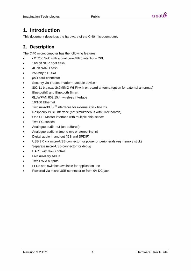
1. Introduction This document describes the hardware of the Ci40 microcomputer.
2. Description The Ci40 microcomputer has the following features:
cXT200 SoC with a dual core MIPS interAptiv CPU
16Mbit NOR boot flash
4Gbit NAND flash
256Mbyte DDR3
sD card connector
Security via Trusted Platform Module device
802.11 b,g,n,ac 2x2MIMO Wi-Fi with on-board antenna (option for external antennas)
Bluetooth® and Bluetooth Smart
6LoWPAN 802.15.4 wireless interface
10/100 Ethernet
Two mikroBUSTM
interfaces for external Click boards
Raspberry Pi B+ interface (not simultaneous with Click boards)
One SPI Master interface with multiple chip selects
Two I2C busses
Analogue audio-out (un-buffered)
Analogue audio-in (mono mic or stereo line-in)
Digital audio in and out (I2S and SPDIF)
USB 2.0 via micro-USB connector for power or peripherals (eg memory stick)
Separate micro-USB connector for debug
UART with flow control
Five auxiliary ADCs
Two PWM outputs
LEDs and switches available for application use
Powered via micro-USB connector or from 9V DC jack

Public Imagination Technologies
Ci40 5 Revision 3.2.132
3. Block Diagram
Imagination Technologies Public
Revision 3.2.132 6 Hardware User Guide
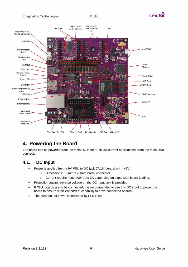
4. Powering the Board The board can be powered from the main DC input or, in low current applications, from the main USB connector.
4.1. DC Input
Power is applied from a 9V PSU to DC jack CN16 (central pin = +9V).
o Dimensions: 5.5mm x 2.1mm barrel connector.
o Current requirement: 400mA to 3A depending on expansion board loading.
Protection against reverse voltage on the DC input jack is provided.
If Click boards are to be connected, it is recommended to use this DC input to power the board to ensure sufficient current capability to drive connected boards.
The presence of power is indicated by LED D16:

Public Imagination Technologies
Ci40 7 Revision 3.2.132
Figure 1 DC Input
CN11 (2 pin 0.1” header) is provided to allow an external power switch to be used. Joining these pins together disables the 5V supply (NB: this only disables power when using the DC jack).
The input is protected with a 1206 surface mount fuse, F1, type 3.5A Fast blow.
o Recommended part: Bel Fuse C1F-3.5A (code 0685F3500)

Imagination Technologies Public
Revision 3.2.132 8 Hardware User Guide
4.2. Powering via USB
The board can be powered from the USB connector, CN40, for low current setups.
It is not recommended to power the board using this method if Click boards are connected because USB ports cannot provide the higher current required.
Figure 2 USB port
Note: power cannot be applied via the debug USB port, CN10.
Public Imagination Technologies
Ci40 9 Revision 3.2.132
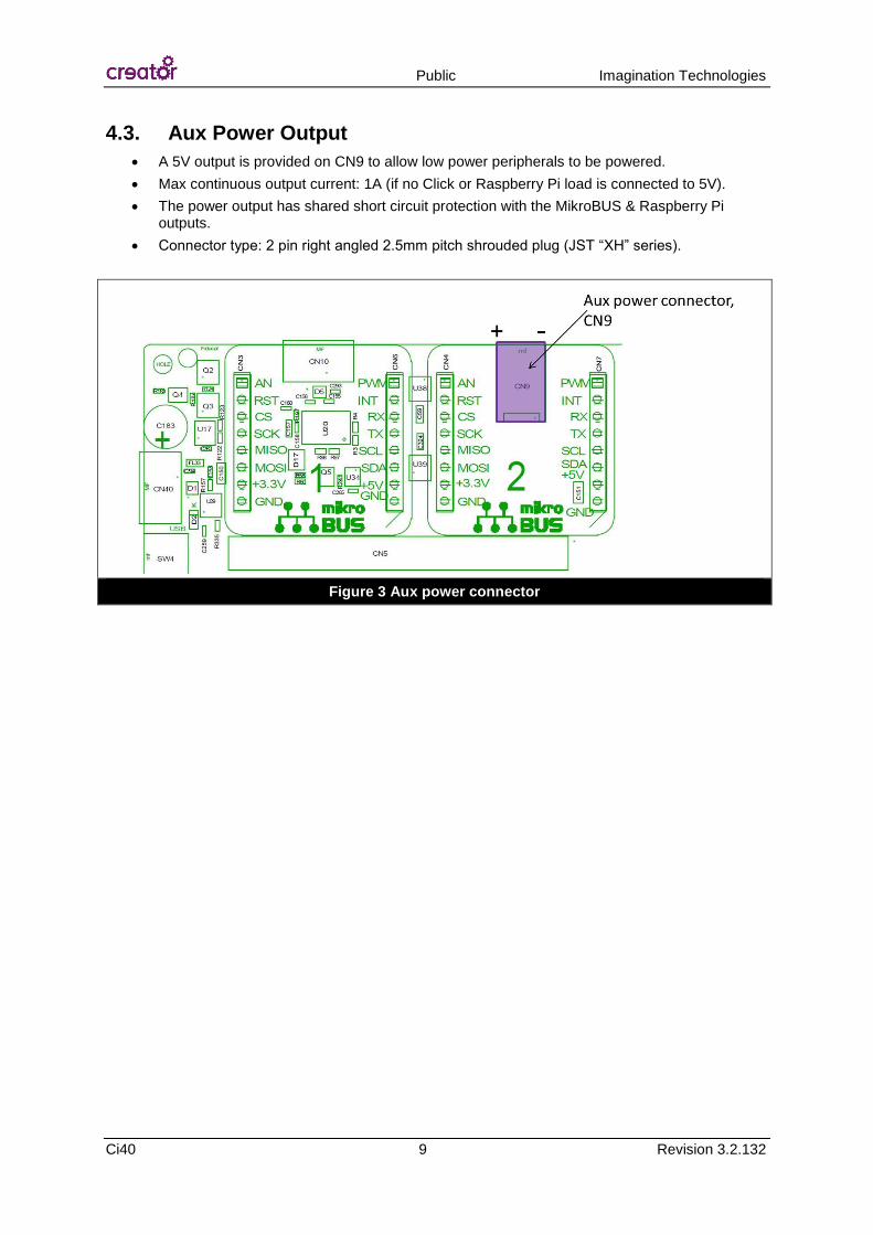
4.3. Aux Power Output
A 5V output is provided on CN9 to allow low power peripherals to be powered.
Max continuous output current: 1A (if no Click or Raspberry Pi load is connected to 5V).
The power output has shared short circuit protection with the MikroBUS & Raspberry Pi outputs.
Connector type: 2 pin right angled 2.5mm pitch shrouded plug (JST “XH” series).
Figure 3 Aux power connector

Imagination Technologies Public
Revision 3.2.132 10 Hardware User Guide
5. Boot Straps The boot mode can be changed between booting from on-module flash, and booting from
JTAG by setting the position of switch SW3 bit2:
1 2
Flash boot
1 2
JTAG boot
Figure 4 Boot mode switches
Note:
Only bit 2 in SW3 affects boot mode. Bit 1 controls the audio ADC input gain.
In JTAG boot mode the mask rom will read the strap and sit in a state spinning.
Public Imagination Technologies
Ci40 11 Revision 3.2.132
6. Reset
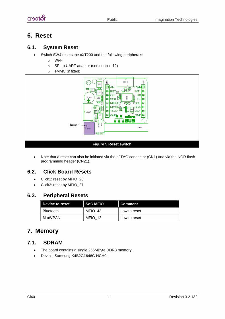
6.1. System Reset
Switch SW4 resets the cXT200 and the following peripherals:
o Wi-Fi
o SPI to UART adaptor (see section 12)
o eMMC (if fitted)
Figure 5 Reset switch
Note that a reset can also be initiated via the eJTAG connector (CN1) and via the NOR flash programming header (CN21).
6.2. Click Board Resets
Click1: reset by MFIO_23
Click2: reset by MFIO_27
6.3. Peripheral Resets
Device to reset SoC MFIO Comment
Bluetooth MFIO_43 Low to reset
6LoWPAN MFIO_12 Low to reset
7. Memory
7.1. SDRAM
The board contains a single 256MByte DDR3 memory.
Device: Samsung K4B2G1646C-HCH9.

Imagination Technologies Public
Revision 3.2.132 12 Hardware User Guide
7.2. NOR Flash
A 16Mbit SPI flash device is used for boot code.
Device: Winbond W25Q16DVSNIG.
It is interfaced to SPI_M1 on the SoC and uses chip select CS0.
7.2.1. NOR Flash programming
The NOR flash can be programmed via CN21.
Connector type: 2x3 0.1” header.
Figure 6 NOR Flash header
The pin-out for the programming header is as follows:
Pin Signal Pin Signal
1 ResetN to Ci40 2 CS0
3 SPI_MClk 4 D1_MISO
5 D0_MOSI 6 GND
To avoid conflict with the cXT200 output, the system must be powered but held in reset during programming by holding the reset input to the programming header low.
Note that x4 transfer is not supported for NOR programming.
7.3. NAND Flash
A 4Gbit SPI NAND flash is used for application code and data storage.
Device: Gigadevice GD5F4GQ4UCYIGT.
This device is not fitted on eMMC versions of board.
It is interfaced to SPIM1 on the cXT200 and uses chip select CS1. It supports x4 read.
The NAND flash is programmed via the cXT200.
7.4. Optional SD Card
Connector CN13 allows a SD card to be connected to the SoC for additional user storage.
SD v3.0 compatible (excluding UHS II).
Bus modes supported: DS and HS.

Public Imagination Technologies
Ci40 13 Revision 3.2.132
Figure 7 SD connector
7.5. Optional eMMC memory
As an alternative to the SD card, a 32Gbit eMMC flash memory can be fitted to Ci40.
Boards supplied with eMMC memory do not have NAND flash installed.
Part number: Samsung KLM4G1FEPD-B031.
eMMC memory is accessed via the cXT200’s sD bus (4 bit mode only).

Imagination Technologies Public
Revision 3.2.132 14 Hardware User Guide
8. RF interfaces
8.1. Wi-Fi
The cXT200 incorporates the Ensigma™ Explorer RPU, a high performance SOC communications platform enabling WiFi 11b/g/a/n/ac and 2x2 MIMO for faster data rates and improved range. On the Ci40 microcomputer, it is combined with an IC containing Ensigma RF transceiver IP to give low power, high-performance, dual-band WLAN 802.11n/ac 2x2 MIMO RF.
Ci40 supports 802.11a/b/g/n/ac standards with transmission & reception in the 2.4GHz (2400MHz to 2483.5MHz) & 5GHz (5150MHz to 5825MHz) ISM bands, up to MCS7 data rates, 20/40MHz channel bandwidths in 2.4GHz band and 20/40/80MHz channel bandwidths in 5GHz band.
The transceiver is 2x2 MIMO with 2 on-board antennas.
8.1.1. Wi-Fi Channels by region
The product is fixed via a different software version for each of the following Wi-Fi region requirements:
Regions 2.4GHz band Wi-Fi Channels
5GHz band Wi-Fi channels
1-13
(2412~2472MHz)
36-48
(5150~5250MHz)
50-64
(5250~5350MHz)
100-140
(5470~5725MHz)
149-161
(5725~5825)
United States
1-11
36-48
(U-NII-1)
50-64
(U-NII-2)
DFS
100-140
(U-NII-2e)
DFS
149-161
(U-NII-3)
Europe 1-13
36-48
Indoor Only
52-64
Indoor Only
DFS / TPC
100-140
DFS / TPC
149-161
SRD
Note 1: DFS = Dynamic Frequency Selection (radar avoidance); TPC = Transmit Power Control; SRD = Short Range Devices 25 mW max power.
8.2. Bluetooth Smart
The Bluetooth shares one antenna with the Wi-Fi, and implements Wi-Fi/BT co-existence.
Part number: CSR8811.
It interfaces to the cXT200 over UART0.
NB: this chip’s reset line is controlled directly from the cXT200, not the reset button (see 6.3).
For normal use, the chip’s reset line must be set high.
8.3. Bluetooth
The board contains a single CSR8811 dual-mode device, which can be used for classic Bluetooth® as well as Bluetooth Smart (Bluetooth Low-Energy).
8.4. 6LoWPAN
A 6LoWPAN 802.15.4 interface is provided with on-board antenna.
Part number: Cascoda CA8210.
It interfaces to the cXT200 on SPIMO.
Public Imagination Technologies
Ci40 15 Revision 3.2.132
o Chip select: SPIM0_CS4 (MFIO_30).
NB: this chip’s reset line is controlled directly from the cXT200, not the reset button (see 6.3).
For normal use, the chip’s reset line must be set high.
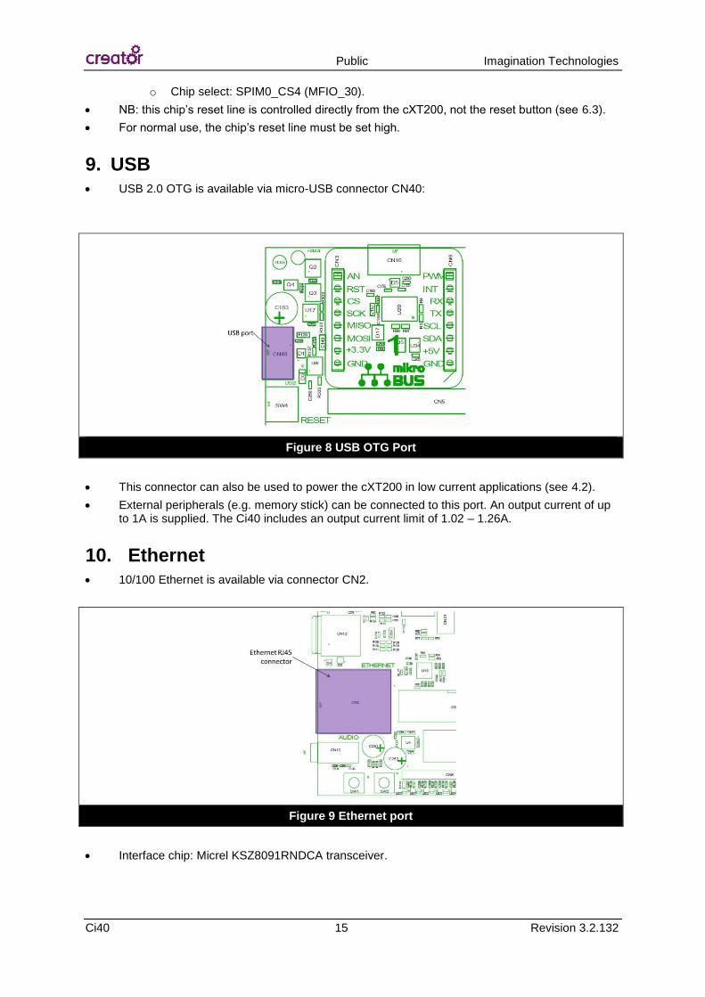
9. USB USB 2.0 OTG is available via micro-USB connector CN40:
Figure 8 USB OTG Port
This connector can also be used to power the cXT200 in low current applications (see 4.2).
External peripherals (e.g. memory stick) can be connected to this port. An output current of up to 1A is supplied. The Ci40 includes an output current limit of 1.02 – 1.26A.
10. Ethernet 10/100 Ethernet is available via connector CN2.
Figure 9 Ethernet port
Interface chip: Micrel KSZ8091RNDCA transceiver.

Imagination Technologies Public
Revision 3.2.132 16 Hardware User Guide
11. MikroBUSTM
Interfaces The Ci40 microcomputer supports two Click add-on boards, connected via CN3/6 and CN4/7.
Note that these cannot be used simultaneously with the Raspberry Pi interface (section 11.2.5).
Note that I2C_2 is also connected to the TPM chip (see section 20).
Note that the SPI bus is shared with on-board peripherals (the 6LoWPAN rf interface, and the SPI-UART adaptor).
Note that the GPIO are not 5V compatible, and applying 5V to those pins may damage the board. Ensure that any GPIO used are 3v3 only.
The 5V output is rated at 1A continuous current (provided the aux power output is not in use)
The 5V output shares common short circuit protection with the Raspberry Pi & Aux power ports.
A list of compatible Click boards can be found at www.imgtec.com/creator/TBA.
11.1. Configuration options
The standard mikroBUS interface as follows is supported on both interfaces:
Click 1
CN3 Signal CN6 Signal
1 Analogue-in to Ci40 (SoC ADC_0) 1 PWM to Click board (SoC PDM_0)
2 Reset to Click board (SoC MFIO_23) 2 Interrupt to Ci40 (SoC MFIO_21)
3 SPI_M0_CS2 3 SoC UART2 Rx
4 SPI_M0_MCLK 4 SoC UART2 Tx
5 SPI_M0_MISO 5 I2C_2_SCL
6 SPI_M0_MOSI 6 I2C_2_SDA
7 3v3 to Click board 7 5V to Click board
8 GND 8 GND
Click 2
CN4 Signal CN7 Signal
1 Analogue-in to Ci40 (SoC ADC_1) 1 PWM to Click board (SoC PDM_1)
2 Reset to Click board (SoC MFIO_27) 2 Interrupt to Ci40 (SoC MFIO_24)
3 SPI_M0_CS3 3 SoC UART3 Rx
4 SPI_M0_MCLK 4 SoC UART3 Tx
5 SPI_M0_MISO 5 I2C_3_SCL
6 SPI_M0_MOSI 6 I2C_3_SDA
7 3v3 to Click board 7 5V to Click board
8 GND 8 GND
Click1 is configured to the standard interface by fitting links between pin 1&2 of JP1-3 and JP7-8.
Click2 is configured to the standard interface by fitting links between pin 1&2 of JP4-6 and JP9-11

Public Imagination Technologies
Ci40 17 Revision 3.2.132
Figure 10 MikroBUS jumpers
The signals going to these interfaces can be reconfigured for Click boards that differ from the above standard. This configuration is done via links according to the following tables:
Click 1
Pin JP Set Signal Pin JP Set Signal
CN3/1 JP1
ADC_0
CN6/1 Non configurable PDM_0 (MFIO_73)
MFIO_22
CN3/2 Non configurable RST (MFIO_23) CN6/2 JP3
INT (MFIO_21)
UART2 CTS
CN3/3 JP2
SPI_M0_CS2
CN6/3 JP8
UART2 Rx
UART2 RTS
MFIO_75
CN3/4 Non configurable SPI_M0_MCLK CN6/4 JP7
UART2 Tx

Imagination Technologies Public
Revision 3.2.132 18 Hardware User Guide
Pin JP Set Signal Pin JP Set Signal
MFIO_14
CN3/5 Non configurable SPI_M0_MISO CN6/5 Non configurable I2C_2_SCL
CN3/6 Non configurable SPI_M0_MOSI CN6/6 Non configurable I2C_2_SDA
Click 2
Pin JP Set Signal Pin JP Set Signal
CN4/1 JP9
ADC_1 CN7/1
Non configurable PDM_1 (MFIO_74)
MFIO_25
CN4/2 Non configurable RST (MFIO_27) CN7/2 JP11
INT (MFIO_24)
UART3 CTS
CN4/3 JP10
SPI_M0_CS3 CN7/3
Non configurable UART3 Rx
UART3 RTS
CN4/4 JP6
SPI_M0_MCLK
CN7/4 Non configurable UART3 Tx
MFIO_31
CN4/5 JP5
SPI_M0_MISO
CN7/5 Non configurable I2C_3_SCL
MFIO_89
CN4/6 JP4
SPI_M0_MOSI
CN7/6 Non configurable I2C_3_SDA

Public Imagination Technologies
Ci40 19 Revision 3.2.132
Pin JP Set Signal Pin JP Set Signal
MFIO_88
11.2. Examples of Jumper settings
11.2.1. MikroBUS 1 Standard Configuration
pin Signal Jumper configuration
CN3/1 ADC_0
CN3/2 RST (MFIO_23)
CN3/3 SPI_M0_CS2
CN3/4 SPI_M0_MCLK
CN3/5 SPI_M0_MISO
CN3/6 SPI_M0_MOSI
CN6/1 PDM_0
CN6/2 INT MFIO_21
CN6/3 UART2 Rx
CN6/4 UART2 Tx
CN6/5 I2C_2_SCL
CN6/6 I2C_2_SDA
11.2.2. MikroBUS 1 UART With Full Flow control
pin Signal Jumper configuration
CN3/1 ADC_0
CN3/2 RST (MFIO_23)
CN3/3 UART2 RTS
CN3/4 SPI_M0_MCLK
CN3/5 SPI_M0_MISO
CN3/6 SPI_M0_MOSI
CN6/1 PDM_0
CN6/2 UART2 CTS
CN6/3 UART2 Rx
CN6/4 UART2 Tx
CN6/5 I2C_2_SCL
CN6/6 I2C_2_SDA
Imagination Technologies Public
Revision 3.2.132 20 Hardware User Guide
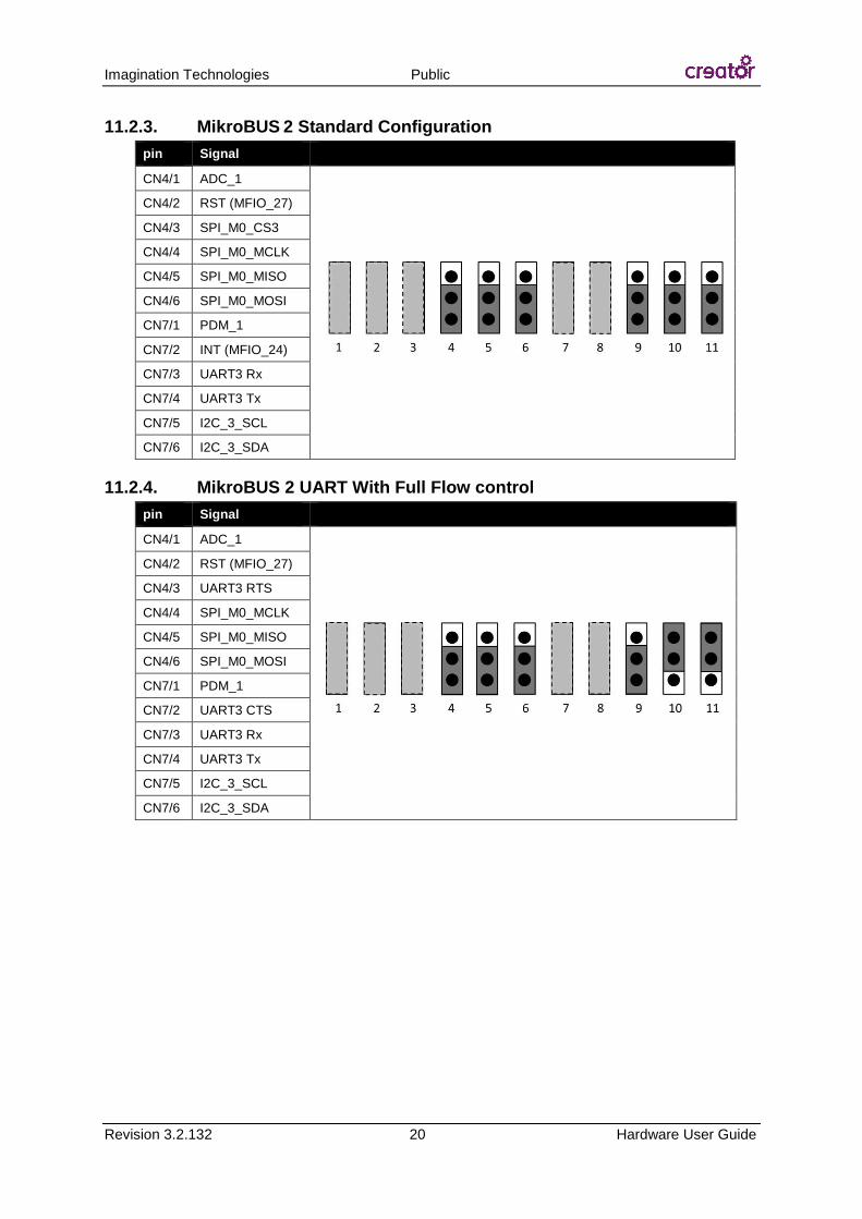
11.2.3. MikroBUS 2 Standard Configuration
pin Signal
CN4/1 ADC_1
CN4/2 RST (MFIO_27)
CN4/3 SPI_M0_CS3
CN4/4 SPI_M0_MCLK
CN4/5 SPI_M0_MISO
CN4/6 SPI_M0_MOSI
CN7/1 PDM_1
CN7/2 INT (MFIO_24)
CN7/3 UART3 Rx
CN7/4 UART3 Tx
CN7/5 I2C_3_SCL
CN7/6 I2C_3_SDA
11.2.4. MikroBUS 2 UART With Full Flow control
pin Signal
CN4/1 ADC_1
CN4/2 RST (MFIO_27)
CN4/3 UART3 RTS
CN4/4 SPI_M0_MCLK
CN4/5 SPI_M0_MISO
CN4/6 SPI_M0_MOSI
CN7/1 PDM_1
CN7/2 UART3 CTS
CN7/3 UART3 Rx
CN7/4 UART3 Tx
CN7/5 I2C_3_SCL
CN7/6 I2C_3_SDA

Public Imagination Technologies
Ci40 21 Revision 3.2.132
11.2.5. Optional Raspberry Pi Interface
The Ci40 supports Raspberry Pi B+ daughterboards.
Note that Raspberry Pi cannot be used simultaneously with either MikroBUS interface.
The 5V output is rated at 1A continuous current (provided the aux power output is not in use).
The 5V output shares common short-circuit protection with the MikroBUS and Aux power ports.
The Raspberry Pi connects to CN5 and is configured by links on jumpers JP1-9.
Figure 11 RPi connector
pin signal pin Signal
1 3v3 to Raspberry Pi board 2 5v to Raspberry Pi board
3 I2C_2 SDA 4 5v to Raspberry Pi board
5 I2C_2 SCLK 6 GND
7 MFIO_22 or ADC0* 8 UART2 TX or MFIO_14
*
9 GND 10 UART2 RX or MFIO_75*
11 MFIO_25 or ADC1* 12 I2C_3_SDA
13 MFIO_23 14 GND
15 MFIO_24 16 I2C_3_SCLK
17 3v3 to Raspberry Pi board 18 PWM_0 (MFIO_73)
19 SPI_M0_MOSI or MFIO_88* 20 GND
21 SPI_M0_MISO or MFIO_89* 22 MFIO_21 or UART2_CTS
*
23 SPI_M0_MCLK or MFIO_ 31* 24 SPI_M0_CS2 (MFIO_28) or UART2 RTS
*
25 GND 26 SPI_M0_CS3 (MFIO_29)
27 Not used 28 Not used
29 MFIO_27 30 GND
31 MFIO_72 32 PWM_1 (MFIO_74)
33 MFIO_80 34 GND
35 MFIO_81 36 MFIO_82
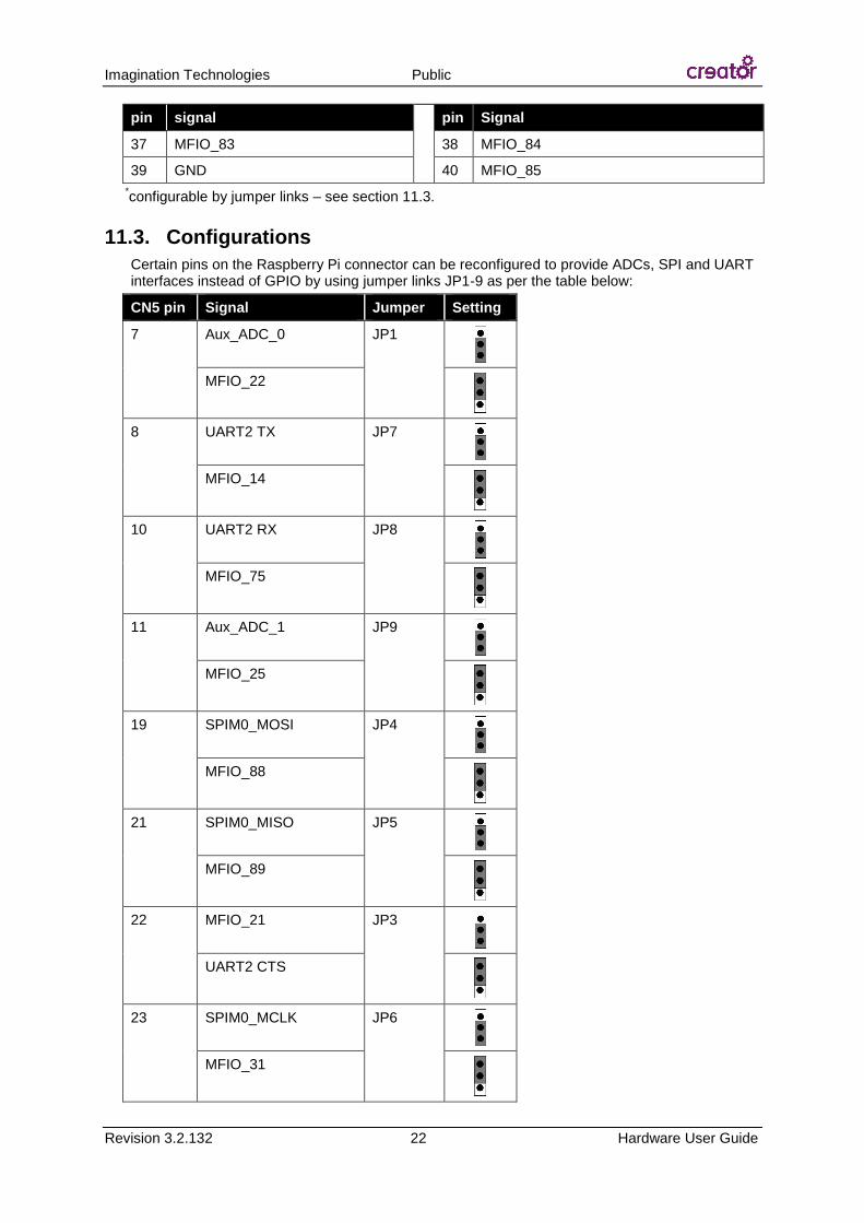
Imagination Technologies Public
Revision 3.2.132 22 Hardware User Guide
pin signal pin Signal
37 MFIO_83 38 MFIO_84
39 GND 40 MFIO_85
*configurable by jumper links – see section 11.3.
11.3. Configurations
Certain pins on the Raspberry Pi connector can be reconfigured to provide ADCs, SPI and UART interfaces instead of GPIO by using jumper links JP1-9 as per the table below:
CN5 pin Signal Jumper Setting
7 Aux_ADC_0 JP1
MFIO_22
8 UART2 TX JP7
MFIO_14
10 UART2 RX JP8
MFIO_75
11 Aux_ADC_1 JP9
MFIO_25
19 SPIM0_MOSI JP4
MFIO_88
21 SPIM0_MISO JP5
MFIO_89
22 MFIO_21 JP3
UART2 CTS
23 SPIM0_MCLK JP6
MFIO_31

Public Imagination Technologies
Ci40 23 Revision 3.2.132
CN5 pin Signal Jumper Setting
24 SPIM0_CS2
(MFIO_28)
JP2
UART2 RTS
Note that the Raspberry Pi interface cannot be used at the same time as the MikroBUS interfaces.
11.3.1. Typical Configurations
UART Configuration
Mode Pin Signal Jumpers
UART with flow control
8 UART2 TX
10 UART2 RX
22 UART2 CTS
24 UART2 RTS
UART without flow control
8 UART2 TX
10 UART2 RX
22 MFIO_21
24 MFIO_28 or SPIM0_CS2
No UART – GPIO configuration
8 MFIO_14
10 MFIO_75 or PWM2
22 MFIO_21
24 MFIO_28 or SPIM0_CS2
SPI Configuration
Mode Pin Signal Jumpers
SPI with 2 chip selects
19 SPI_M0_MOSI
21 SPI_M0_MISO
23 SPI_M0_MCLK
24 SPI_M0_CS2
26 SPI_M0_CS3
SPI with CS2 only
19 SPI_M0_MOSI
(pin 26 is configured in software, not hardware)
21 SPI_M0_MISO
23 SPI_M0_MCLK
24 SPI_M0_CS2
26 MFIO_29
SPI with CS3 only
19 SPI_M0_MOSI (pin 24 is changed from CS to MFIO in software)
21 SPI_M0_MISO

Imagination Technologies Public
Revision 3.2.132 24 Hardware User Guide
Mode Pin Signal Jumpers
23 SPI_M0_MCLK
24 MFIO_28
26 SPI_M0_CS3
No SPI – GPIO only
19 MFIO_88
21 MFIO_89
23 MFIO_ 31
24 MFIO_28
26 MFIO_29
Configuration to use ADCs
Mode Pin Signal Jumpers
Two ADCs 7 ADC_0
11 ADC_1
ADC_0 only 7 ADC_0
11 MFIO_25
ADC_1 only 7 MFIO_22
11 ADC_1
No ADCs – GPIO only
7 MFIO_22
11 MFIO_25
12. SPI-UART Adaptor
The UARTs to the MikroBUS and Raspberry Pi interfaces originate from U12, an SPI-UART adaptor (an NXP SC16IS752IPW) connected to SPIM0.
SPI Chip select: SPIM0_CS0 (MFIO_2).
LEDs 0-6 are driven from the adaptor’s GPIO.
13. I2C
The Ci40’s I2C busses are allocated as follows:
Bus Allocation Section Comment
I2C_0 Not available n/a
I2C_1 Not available n/a
I2C_2 TPM & MikroBUS /RPi interfaces 11, 11.2.5 & 20 Address of TPM on I2C_2 is 0x20
I2C_3 MikroBUS /RPi interfaces 11 & 11.2.5

Public Imagination Technologies
Ci40 25 Revision 3.2.132
14. SPI The Ci40’s SPI busses are allocated as follows:
Bus Chip Select Allocation Section
SPI_M0 CS0 UART expander 12
CS1 Not available n/a
CS2-3 MikroBUS & Raspberry Pi interfaces 11 & 11.2.5
CS4 6LoWPAN control 8.4
SPI_M1 CS0 NOR flash 7.2
CS1 NAND flash 7.3
CS2 Not available n/a
15. Analogue Inputs
Ci40 has five 10 bit auxiliary ADC inputs for monitoring dc voltages.
Note that each ADC input is passed through a potential divider:
Due to this input scaling, the voltage on Aux_ADC input = 0.357 x Vin.
Max input to SoC AUX_ADC input: 1.8 V.
Max input to connector AuxADC lines: 5.0 V.
Input impedance presented at the connector: 28K.
ADC_0 & ADC_1 connect to the MikroBUS and Raspberry Pi interfaces (sections 11 and 11.2.5).
ADC_2, ADC_3 and ADC_5 are routed to a 4-pin 2.54mm SIL header, CN17.
Figure 12 Analogue inputs
Pin Signal
1 AUX_ADC_2

Imagination Technologies Public
Revision 3.2.132 26 Hardware User Guide
Pin Signal
2 AUX_ADC_3
3 AUX_ADC_5
4 GND
16. PWM_PDM Outputs Two PWM/PDM outputs route to the MikroBUS and Raspberry Pi interfaces (see sections 11 &
11.2.5) .

Public Imagination Technologies
Ci40 27 Revision 3.2.132
17. LEDs & Switches Ci40 supports on-board and external LEDs and switches.
Figure 13 LEDs and switches
17.1. On-board LEDs
Ci40 has 8 on-board indicator LEDs.
LEDs 0 – 6 are driven from the SPI-UART adaptor (see 12).
The “heartbeat” LED is connected to one of the cXT200’s PWM/PDM outputs:
LED Control line Comment
LED0 U12 GPIO_0 Low output to illuminate
LED1 U12 GPIO_1 Low output to illuminate
LED2 U12 GPIO_2 Low output to illuminate
LED3 U12 GPIO_3 Low output to illuminate
LED4 U12 GPIO_4 Low output to illuminate
LED5 U12 GPIO_5 Low output to illuminate
LED6 U12 GPIO_6 Low output to illuminate
PWM3/”heartbeat” SoC PWM_3 High output to illuminate
17.2. On-board Switches
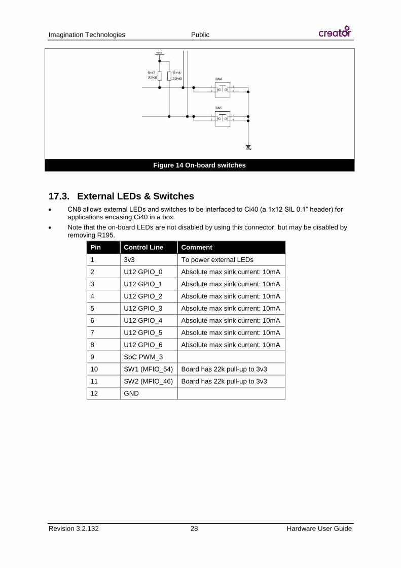
Ci40 has 2 tact switches that connect directly to the cXT200:
switch cXT200 input Comment
SW1 MFIO_54 Push takes SoC i/p low
SW2 MFIO_46 Push takes SoC i/p low
Imagination Technologies Public
Revision 3.2.132 28 Hardware User Guide
Figure 14 On-board switches
17.3. External LEDs & Switches
CN8 allows external LEDs and switches to be interfaced to Ci40 (a 1x12 SIL 0.1” header) for applications encasing Ci40 in a box.
Note that the on-board LEDs are not disabled by using this connector, but may be disabled by removing R195.
Pin Control Line Comment
1 3v3 To power external LEDs
2 U12 GPIO_0 Absolute max sink current: 10mA
3 U12 GPIO_1 Absolute max sink current: 10mA
4 U12 GPIO_2 Absolute max sink current: 10mA
5 U12 GPIO_3 Absolute max sink current: 10mA
6 U12 GPIO_4 Absolute max sink current: 10mA
7 U12 GPIO_5 Absolute max sink current: 10mA
8 U12 GPIO_6 Absolute max sink current: 10mA
9 SoC PWM_3
10 SW1 (MFIO_54) Board has 22k pull-up to 3v3
11 SW2 (MFIO_46) Board has 22k pull-up to 3v3
12 GND

Public Imagination Technologies
Ci40 29 Revision 3.2.132
18. Programming
18.1. NOR Flash programming
The NOR boot flash can be reprogrammed via the cXT200. Alternatively, a programmer can be directly connected via CN21:
Pin Function Pin Function
1 ResetN 2 CS
3 MCLK 4 MISO
5 MOSI 6 GND
Figure 15 NOR Flash programming connector
Connector type: 2x3 0.1” header.
To avoid possible bus conflict, it is recommended that the cXT200 be held in reset during this process. This will be done by holding CN21 pin1 low.
If write-protection is enabled in the NOR flash, holding the board in reset will also release the device’s write protect.
18.2. NAND Flash programming
The NAND flash should be programmed via software running on the cXT200 in order to utilise bad block management.

Imagination Technologies Public
Revision 3.2.132 30 Hardware User Guide
19. Debug
19.1. UART Debug Port
Debug is provided via UART-over-USB.
UART to USB interface chip: FTDI FT230XS-R.
The adaptor chip is connected to the cXT200’s UART1 port.
This debug interface is connected to the micro-USB connector, CN10.
Please note that this is the only function for this connector, and the board cannot be powered via this connector.
Figure 16 UART debug port

Public Imagination Technologies
Ci40 31 Revision 3.2.132
19.2. eJTAG interface
A MIPS eJTAG interface is provided on CN1 with pin-out as follows:
Figure 17 JTAG port
Note that Vio includes short circuit protection (nominal 200mA trip).
19.2.1. Connecting JTAG probes to the JTAG port
The Ci40 SoC has multiple TAPs on the JTAG chain. Most probes will require a configuration file describing the JTAG chain layout. The information required is below:
Number of TAPS
6
IR Length of each TAP
5 bits
TAP layout
TAP 0 is a MIPS32 TAP with JTAG ID of 0x04320c33
TAP 1 is a MIPS32 TAP with JTAG ID of 0x04321c33
TAP 2 is a MIPS32 TAP with JTAG ID of 0x14320c33
TAP 3 is a MIPS32 TAP with JTAG ID of 0x14321c33
TAP 4 is a MIPS CM TAP with JTAG ID 0x34321c33
TAP 5 is a IMG META/UCC TAP with JTAG ID of 0x1ffff11d
Imagination Technologies Public
Revision 3.2.132 32 Hardware User Guide
20. Security A TPM device (Infineon SLB9645VQ1.2) is connected to the SoC over I
2C.
The I2C address allocated to the TPM on I2C_2 is 0x20.
Note that I2C_2 is shared with the MikroBUS 1 & Raspberry Pi interface. Signal contentions will occur if a connected daughterboard uses those lines as GPIO. If those lines are used as GPIO, it is important to hold the TPM in its reset state.
The reset line RST_N is connected to SoC MFIO_42.
The DAVINT_N line is connected to SoC MFIO_13.

Public Imagination Technologies
Ci40 33 Revision 3.2.132
21. Digital Audio The Ci40 has digital audio in and out (I
2S and SPDIF), available on CN15:
Figure 18 Digital audio – I2S and SPDIF
Connector type: 2x10 0.1” IDC shrouded header
Pin Signal Pin Signal
1 I2S_OUT_D2 2 GND
3 I2S_OUT_D1 4 I2S_OUT_D0
5 I2S_OUT_LRCLK 6 GND
7 I2S_OUT_BCLK 8 I2S_OUT_MCLK
9 I2S_IN_BCLK 10 GND
11 I2S_IN_LRCLK 12 I2S_IN_D0
13 I2S_IN_D1 14 GND
15 I2S_IN_D32 16 I2S_IN_D4
1
17 I2S_DAC_CLK3 18 GND
19 SPDIF_OUT* 20 SPDIF_IN*1
*should be connected to an external coax driver chip or optical interface chip. I2S_DAC_CLK is an alternative MCLK source that can be set to a different clock frequency. 1on iss4 and earlier, this is GND
2on iss4 and earlier, this is I2S_IN_D2
3on iss4 and earlier, this is SPDIF_IN*

Imagination Technologies Public
Revision 3.2.132 34 Hardware User Guide
22. Analogue Audio Analogue audio-in and -out are supported via a four terminal 3.5mm socket CN12 on the top of
the board, and via pads on the underside of the PCB (TP40-42):
Figure 19 Analog audio circuit
Figure 20 Analog audio connectors
CN12 is CTIA compatible*:

Public Imagination Technologies
Ci40 35 Revision 3.2.132
Figure 21 Audio plug compatibility
*NB: on the iss4 board, CN12 is OMTP compatible, not CTIA (i.e. mic and ground are switched)!
22.1. Analogue Audio in
The Creator Ci40 is equipped with an audio ADC (AKM AK5720) to allow analogue audio to be fed into the cXT200’s I2S_D2 I
2S input.
The ADC is enabled by setting IC_ADC_PDN_N (U12/GPIO7) “high”.
Note that CN12 only supports a mono microphone. For stereo analogue audio in, it is necessary to use pads TP40-42.
The mono microphone input on CN12 is connected to the left channel.
Note that the mono microphone input is directly connected to the left audio input. If using the stereo input connections, it is recommended to remove link R94 to isolate the audio paths (see above for location of R94).
Full scale audio input levels: 2V peak-to-peak.
A 3v3 mic bias is applied to audio-in left and right via 2k2 resistors.
When used with a microphone, the internal gain of the ADC should be set to “high” by setting SW3 bit1 to “on”. This provides 15dB gain used when connecting a microphone/headset to the jack connector. In addition, you can implement a further 10dB of digital gain within the cXT200.
1 2
SW3
ON
Figure 22 Analog audio in switches
22.2. Analogue Audio Out
The cXT200’s internal mid-performance audio DAC is connected to 3.5mm socket CN12 via a 100mW audio headphone amplifier.
The amplifier is enabled by setting MFIO_79 low.
The audio output spec is as follows:
o Drive capability: max 40mW RMS per channel (1kHz into 16 load @ 0.1% THD).
o Minimum load resistance: 8.
Imagination Technologies Public
Revision 3.2.132 36 Hardware User Guide
23. Glossary
MFIO
RPU
Multi-Purpose Input/Output: these pins can be configured as GPIO or as other functions such as bus interfaces.
Radio Processing Unit