circuit design for testing standard cell libraries design for testing standard cell libraries ......
TRANSCRIPT

Circuit Design for Testing Standard Cell Libraries
Renato P. Ribas1,2, Vinicius Callegaro
2, Marcelo Lubaszewski
2, André Ivanov
1, André I. Reis
2
1ECE / University of British Columbia
2356 Main Mall
Vancouver, BC, V6T 1Z4, Canada
2Federal University of Rio Grande do Sul
Av. Bento Gonçalves, 9500
Porto Alegre, RS, 91501-970, Brazil
Email: [email protected]
ABSTRACT
This work presents the design methodology and the architecture
of simple, efficient and easy-to-use test circuits for evaluating and
validating any set of library cells (combinational and sequential
logic gates), both in the design environment and for on silicon
prototyping. Evaluation and validation are accomplished
considering functionality, performance, power consumption and
impact in operation of nanometer aging effects. Simulation results
demonstrate the behavior of the proposed design and the many
facilities it provides.
Categories and Subject Descriptors
B.8.2 [Logic Design]: Reliability and Testing – built-in tests,
error-checking, test generation, testability.
General Terms
Design, Verification.
Keywords
Standard cell library, digital circuit, logic gates, self-timed, self-
checking, functional test, delay test, aging evaluation.
1. INTRODUCTION The cell-based approach is definitely the most applied strategy to
ASIC design nowadays. This top-down integrated circuit (IC)
design methodology considers the reuse of library cells to build
more complex digital circuits. In standard cells IC flow, as the
technology mapping task is based on pre-characterized data from
pre-designed logic gates, the ASIC design space and efficiency
turns to be bounded by the profile of the library targeted.
The availability of distinct logic functions, including different cell
drive strength options, potentially increases the possibilities for
design quality improvement. The composition of libraries may
vary according to the designer requirements and application
constraints. Some approaches advocate the use of reduced set of
cells [1], while others consider larger libraries in order to bring
more design flexibility [2].
In anyway, at any library based approach, the complete electrical
characterization of logic gates is required before applying them in
the IC design flow. Such characterization shall be accurately
performed by considering different signal input slopes, output
capacitive loads and design corners (temperature, power supply
and process parameters variation), for both timing (delay
propagation and output transition) and power dissipation (static
and dynamic components). Electrical characteristics, together with
cell area, are essential for the circuit mapping procedure, static
timing analysis (STA) and power consumption estimation. These
data are usually provided by automatic library generators and
characterization tools, being available in standard formats like
Liberty, LEF/DEF and GDSII files, since such a kind of
information is provided in a per cell basis. Hence, the target
library must be carefully verified and validated in the EDA
environment (models data and description files) as well as on
silicon [3][4].
In standard cell libraries, three groups of logic gates co-exist: (1)
inverters/buffers; (2) combinational cells and (3) storage elements
(latches and flip-flops). Mainly due to the large number of
different logic functions and driving strength options needed in
typical designs, the largest of the three aforementioned groups is
the set of combinational logic gates. The handcraft creation of
libraries demands skilled designers and long development time,
even when simply dealing with technology migration for the same
set of cells. In practice, the high engineering costs of such tasks
imposes a limitation on the quantity of gates available in libraries.
Furthermore, it is worth to mention that current mapping engines
do not manage efficiently huge libraries due to the large amount
of data concerned.
In this work, a design methodology to automatically produce test
circuits is presented for complete functional and electrical
validation of any kind of set of gates. It presents straightforward
operating and monitoring procedures, being suitable to evaluate
libraries at EDA level as well as at on silicon level. At EDA level,
the proposed methodology is useful to validate the library files in
the design environment, checking the accuracy of electrical data,
i.e., delay and power cell models, and the correlation to STA and
power prediction, respectively. The resulting circuit can also act
as benchmarking to compare different layout templates and
transistor topologies for the same set of cells. At on silicon prove,
the main goal is to provide a solution with limited number of I/O
pads and minimum use of ATE (automatic test equipment) tools,
reducing significantly the test engineering costs. Additionally, the
test circuits are useful as a monitoring scheme to evaluate the
impact in design of emerging nanometer aging mechanisms, by
exploiting the intermittent circuit execution through the self-timed
operating mode.
In Section 2 is discussed the general purpose of this work.
Combinational gates are treated in Section 3. A CAD tool has
been developed to generate automaticaly the functional blocks
according to the set of combinational cells available in a target
library. Section 4 describes the test circuits for sequential cells
(latches and flip-flops). Some experimental results are shown in
Section 5. The conclusions are outlined in Section 6.

2. PRELIMINARIES First of all, the first group of gates composed by inverters and
buffers is easily tested in all different aspects (functionality, delay
propagation and power dissipation) through standard ring
oscillators, due to the existence of a single input signal.
In the case of combinational multi-input gates, all possible input
vectors should be stimulated and verified. The most
straightforward way that can be thought to design a test circuit for
an ensemble of logic cells consists in instantiating all gates in
parallel arrangement, using shared primary inputs (for test
controllability) while individual output signals may be
multiplexed in order to reduce the quantity of I/O pads, without
loosing test observability. Such a strategy can obviously provide
full functional validation of each logic gate under test. However,
timing information is quite difficult to be obtained through a
circuit presenting only one level of logic depth. Additionally, the
multiplexers at the output, the input buffering to compensate the
high capacitance on input nodes, and the packaging parasitic
elements make this approach impractical to extract timing values.
When addressing sequential cells (latches and flip-flops), besides
the input state, the stored data can become the most critical
challenge for such library evaluation and validation.
Another challenge for library validation is the reliability test
(DFM failures and aging effects), usually based on the continuous
application of input stimuli and output signals monitoring. Such
procedure increases significantly the cost of ATE.
An approach that can make these tests viable without additional
ATE is strongly desirable. One possibility would be to design an
application circuit whose functionality could be easily verified.
Tape-outs of benchmark circuits (open cores) for verification and
validation of standard cell libraries is a common applied strategy.
However, it is importante to notice that the instantiation at least
once of all cells available in the library under test is rarely attained
during the circuit mapping. Furthermore, even if a mapped circuit
had presented at least one instantiation of every cell, full
functional stimuli of each of them cannot be guaranteed.
The general structure of the test circuits proposed for evaluation
and validation of cell libraries is illustrated in Fig. 1, and the aims
can be summarized as follows:
• fully functional behavior verification by stimuling all
possible static states and transitions;
• validation of cell delay and power models, and data used in
the library description;
• simple test circuit for validation of library files required in
the design environment;
• simple test circuit for on-silicon validation of cell libraries
(minimum use of ATE);
• continuous test circuit execution for aging analysis.
Moreover, there are two different operation modes of these
circuits:
a) Asynchronous (self-timed) circuit operation
• minimum ATE intervention (no input stimuli during the test
execution)
• self-checking circuit run (auto-stopping due to functional
error)
• performance analysis (correlation of on-silicon
measurements and electrical simulations)
• aging evaluation (continuous circuit running and speed
monitoring)
b) Synchronous (clocked) circuit operation
• use of extenal clock signal;
• step-by-step execution for steady state analysis (leakage and
long term data retention);
• power consumption analysis related to the circuit operation
frequency;
• diagnosis mode in case of functional error.
Figure 1. General model of the proposed test circuits.
3. COMBINATIONAL CELLS The combinational blocks, depicted in Fig. 2, are the key elements
of the test circuit effectiveness. They are built in a way to
guarantee the application of complete functional stimuli on the
ensemble of logic gates to be verified.
Figure 2. Example of a 3-input combinational block.
In the first stage, a subset of cells under test is placed in parallel
arrangement, composing a single logic depth circuit. The primary
block inputs (‘IN’) are directly connected to (and shared by) the
inputs of these cells (‘Ci’). The output data of such stage, here
identified as ‘W’ vector, is resulted from the functional behavior
of the instantiated cells. The second stage, in turn, receives the
intermediate code ‘W’ and produces the block output data ‘Out’.
The ‘Out’ vector is made equivalent to the ‘IN’ one, i.e., IN≡Out.
It is done by synthesizing a multi-level circuit considering such
specification and the information from ‘W’ vector.
Based on the characteristics of the combinational blocks,
described above, the test circuit architecture is proposed, as
depicted in Fig. 3.
The combinational blocks are cascaded expecting the data at the
beginning of the chain ‘In(n..1)’ is reproduced at the end of that in
‘Out(n..1)’ nodes, whether no functional error occurs in the cells
under test. To provide a sequence of test vectors with minimum
external intervention, the signals at the end of the combinational
chain are reconnected to the beginning of it in a ring
configuration. Multiplexers are placed in the combinational chain
avoiding blocks in the logical path when desired. Register barriers
(D-type flip-flops – ‘DFF’) are introduced into the feedback path
to avoid racing. The adder block is also included in the ring to
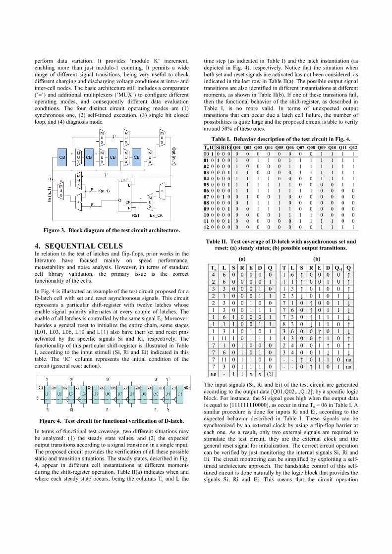
perform data variation. It provides ‘modulo K’ increment,
enabling more than just modulo-1 counting. It permits a wide
range of different signal transitions, being very useful to check
different charging and discharging voltage conditions at intra- and
inter-cell nodes. The basic architecture still includes a comparator
(‘=’) and additional multiplexers (‘MUX’) to configure different
operating modes, and consequently different data evaluation
conditions. The four distinct circuit operating modes are (1)
synchronous one, (2) self-timed execution, (3) single bit closed
loop, and (4) diagnosis mode.
Figure 3. Block diagram of the test circuit architecture.
4. SEQUENTIAL CELLS In relation to the test of latches and flip-flops, prior works in the
literature have focused mainly on speed performance,
metastability and noise analysis. However, in terms of standard
cell library validation, the primary issue is the correct
functionality of the cells.
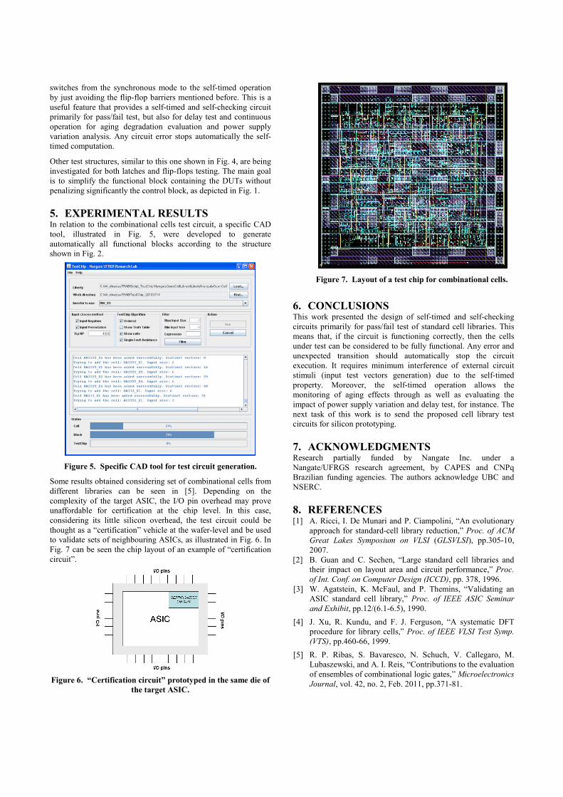
In Fig. 4 is illustrated an example of the test circuit proposed for a
D-latch cell with set and reset asynchronous signals. This circuit
represents a particular shift-register with twelve latches whose
enable signal polarity alternates at every couple of latches. The
enable of all latches is controlled by the same signal Ei. Moreover,
besides a general reset to initialize the entire chain, some stages
(L01, L03, L06, L10 and L11) also have their set and reset pins
activated by the specific signals Si and Ri, respectively. The
functionality of this particular shift-register is illustrated in Table
I, according to the input stimuli (Si, Ri and Ei) indicated in this
table. The ‘IC’ column represents the initial condition of the
circuit (general reset action).
Figure 4. Test circuit for functional verification of D-latch.
In terms of functional test coverage, two different situations may
be analyzed: (1) the steady state values, and (2) the expected
output transitions according to a signal transition in a single input.
The proposed circuit provides the verification of all these possible
static and transition situations. The steady states, described in Fig.
4, appear in different cell instantiations at different moments
during the shift-register operation. Table II(a) indicates when and
where each steady state occurs, being the columns Tn and L the
time step (as indicated in Table I) and the latch instantiation (as
depicted in Fig. 4), respectively. Notice that the situation when
both set and reset signals are activated has not been considered, as
indicated in the last row in Table II(a). The possible output signal
transitions are also identified in different instantiations at different
moments, as shown in Table II(b). If one of these transitions fail,
then the functional behavior of the shift-register, as described in
Table I, is no more valid. In terms of unexpected output
transitions that can occur due a latch cell failure, the number of
possibilities is quite large and the proposed circuit is able to verify
around 50% of these ones.
Table I. Behavior description of the test circuit in Fig. 4.
Tn IC Si Ri Ei Q01 Q02 Q03 Q04 Q05 Q06 Q07 Q08 Q09 Q10 Q11 Q12
00 1 0 0 0 0 0 0 0 0 0 0 0 1 1 1 1
01 0 1 0 0 1 0 1 1 0 1 1 1 1 1 1 1
02 0 0 0 0 1 0 0 0 0 1 1 1 1 1 1 1
03 0 0 0 1 1 1 0 0 0 0 1 1 1 1 1 1
04 0 0 0 0 1 1 1 1 0 0 0 0 1 1 1 1
05 0 0 0 1 1 1 1 1 1 1 0 0 0 0 1 1
06 0 0 0 0 1 1 1 1 1 1 1 1 0 0 0 0
07 0 0 1 0 0 1 0 0 1 0 0 0 0 0 0 0
08 0 0 0 0 0 1 1 1 1 0 0 0 0 0 0 0
09 0 0 0 1 0 0 1 1 1 1 0 0 0 0 0 0
10 0 0 0 0 0 0 0 0 1 1 1 1 0 0 0 0
11 0 0 0 1 0 0 0 0 0 0 1 1 1 1 0 0
12 0 0 0 0 0 0 0 0 0 0 0 0 1 1 1 1
Table II. Test coverage of D-latch with asynchronous set and reset: (a) steady states; (b) possible output transitions.
(a) (b)
Tn L S R E D Q
4 6 0 0 0 0 0
2 6 0 0 0 0 1
3 3 0 0 0 1 0
2 1 0 0 0 1 1
2 3 0 0 1 0 0
1 3 0 0 1 1 1
1 6 1 0 0 0 1
1 1 1 0 0 1 1
1 3 1 0 1 0 1
1 11 1 0 1 1 1
7 1 0 1 0 0 0
7 6 0 1 0 1 0
7 11 0 1 1 0 0
7 3 0 1 1 1 0
na - 1 1 x x (?)
T L S R E D Q-1 Q
1 6 ↑ 0 0 0 0 ↑
1 1 ↑ 0 0 1 0 ↑
1 3 ↑ 0 1 0 0 ↑
2 3 ↓ 0 1 0 1 ↓
7 1 0 ↑ 0 0 1 ↓
7 6 0 ↑ 0 1 1 ↓
7 3 0 ↑ 1 1 1 ↓
8 3 0 ↓ 1 1 0 ↑
3 6 0 0 ↑ 0 1 ↓
4 3 0 0 ↑ 1 0 ↑
2 4 0 0 1 ↑ 0 ↑
3 4 0 0 1 ↓ 1 ↓
- - ↑ 0 1 1 0 na
- - 0 ↑ 1 0 1 na
The input signals (Si, Ri and Ei) of the test circuit are generated
according to the output data [Q01,Q02,..,Q12], by a specific logic
block. For instance, the Si signal goes high when the output data
is equal to [111111110000], as occur in time Tn = 06 in Table I. A
similar procedure is done for inputs Ri and Ei, according to the
expected behavior described in Table I. These signals can be
synchronized by an external clock by using a flip-flop barrier at
each one. As a result, only two external signals are required to
stimulate the test circuit, they are the external clock and the
general reset signal for initialization. The correct circuit operation
can be verified by just monitoring the internal signals Si, Ri and
Ei. The circuit monitoring can be simplified by exploiting a self-
timed architecture approach. The handshake control of this self-
timed circuit is done naturally by the logic block that provides the
signals Si, Ri and Ei. This means that the circuit operation
switches from the synchronous mode to the self-timed operation
by just avoiding the flip-flop barriers mentioned before. This is a
useful feature that provides a self-timed and self-checking circuit
primarily for pass/fail test, but also for delay test and continuous
operation for aging degradation evaluation and power supply
variation analysis. Any circuit error stops automatically the self-
timed computation.
Other test structures, similar to this one shown in Fig. 4, are being
investigated for both latches and flip-flops testing. The main goal
is to simplify the functional block containing the DUTs without
penalizing significantly the control block, as depicted in Fig. 1.
5. EXPERIMENTAL RESULTS In relation to the combinational cells test circuit, a specific CAD
tool, illustrated in Fig. 5, were developed to generate
automatically all functional blocks according to the structure
shown in Fig. 2.
Figure 5. Specific CAD tool for test circuit generation.
Some results obtained considering set of combinational cells from
different libraries can be seen in [5]. Depending on the
complexity of the target ASIC, the I/O pin overhead may prove
unaffordable for certification at the chip level. In this case,
considering its little silicon overhead, the test circuit could be
thought as a “certification” vehicle at the wafer-level and be used
to validate sets of neighbouring ASICs, as illustrated in Fig. 6. In
Fig. 7 can be seen the chip layout of an example of “certification
circuit”.
Figure 6. “Certification circuit” prototyped in the same die of
the target ASIC.
Figure 7. Layout of a test chip for combinational cells.
6. CONCLUSIONS This work presented the design of self-timed and self-checking
circuits primarily for pass/fail test of standard cell libraries. This
means that, if the circuit is functioning correctly, then the cells
under test can be considered to be fully functional. Any error and
unexpected transition should automatically stop the circuit
execution. It requires minimum interference of external circuit
stimuli (input test vectors generation) due to the self-timed
property. Moreover, the self-timed operation allows the
monitoring of aging effects through as well as evaluating the
impact of power supply variation and delay test, for instance. The
next task of this work is to send the proposed cell library test
circuits for silicon prototyping.
7. ACKNOWLEDGMENTS Research partially funded by Nangate Inc. under a
Nangate/UFRGS research agreement, by CAPES and CNPq
Brazilian funding agencies. The authors acknowledge UBC and
NSERC.
8. REFERENCES [1] A. Ricci, I. De Munari and P. Ciampolini, “An evolutionary
approach for standard-cell library reduction,” Proc. of ACM
Great Lakes Symposium on VLSI (GLSVLSI), pp.305-10,
2007.
[2] B. Guan and C. Sechen, “Large standard cell libraries and
their impact on layout area and circuit performance,” Proc.
of Int. Conf. on Computer Design (ICCD), pp. 378, 1996.
[3] W. Agatstein, K. McFaul, and P. Themins, “Validating an
ASIC standard cell library,” Proc. of IEEE ASIC Seminar
and Exhibit, pp.12/(6.1-6.5), 1990.
[4] J. Xu, R. Kundu, and F. J. Ferguson, “A systematic DFT
procedure for library cells,” Proc. of IEEE VLSI Test Symp.
(VTS), pp.460-66, 1999.
[5] R. P. Ribas, S. Bavaresco, N. Schuch, V. Callegaro, M.
Lubaszewski, and A. I. Reis, “Contributions to the evaluation
of ensembles of combinational logic gates,” Microelectronics
Journal, vol. 42, no. 2, Feb. 2011, pp.371-81.