circuit interfaces and optimiza tion for resistive nanosensors
TRANSCRIPT
Circuit Interfaces and Optimization for Resistive Nanosensors
Rajeevan Amirtharajaha, Albert Chena, Darshan Thakerb, and Frederic T. Chongc
aDept. of Electrical and Computer Engineering, Univ. of California, Davis, One Shields Ave.,Davis, CA, USA;
bDept. of Computer Science, Univ. of California, Davis, One Shields Ave., Davis, CA, USA;cDept. of Computer Science, Engineering I, Univ. of California, Santa Barbara, Santa
Barbara, CA, USA;
ABSTRACT
Carbon nanotube and semiconductor nanowires could potentially usher in a new era in chemical detection forenvironmental, biomedical, and security applications by providing highly sensitive detection at very low cost.For wireless sensor networks and implantable biomedical sensing devices, system power consumption is a criticalfactor in determining volume, operating lifetime, and circuit performance. We describe several key circuitchallenges related to interfacing variable resistance nanosensors to digital integrated circuits through analog-to-digital data conversion. These challenges include drift in nanosensor baseline resistance due to fabricationvariances and incomplete chemical desorption, various sensor and circuit noise sources, and integrated sensorand circuit area and power tradeoffs. We describe and evaluate the potential of several circuit techniques toaddress these issues, including self-test, self-calibration, and noise cancellation. Simulations indicate that ±40%variations in fabricated baseline resistance can be reduced to ±2% with a 25% increase in sensing area using aconfigurable sensor design. Based on these results, we explore potential A/D converter architectures for theiruse as low power nanosensor interfaces. Finally, we discuss resolution limits to miniaturization of nanosensorinterface circuits.
Keywords: Circuits, nanosensor, bridge sensors, analog-to-digital conversion
1. INTRODUCTION
Detection of specific molecules is a critical operation in environmental monitoring, missions in space, controlof chemical processes, and many medical and agricultural applications. We propose a sensor architecture thatleverages nanoscale sensing elements and deep submicron CMOS transistors to produce inexpensive, long lifetimegas-sampling devices. At the core of our architecture is the principle of self-calibration. We design a system thatadjusts for both fabrication variations and partially saturated sensors.
The high surface area-to-volume ratio of nanomaterials allows them to detect very low gas concentrations,enabling sensors with high sensitivity, but offering other advantages as well. Traditional gas sensors are either timeor power intensive. As gases bond to a sensing medium, the sensor becomes saturated and loses its capabilityto detect small concentrations. These bonds are broken over an exponential amount of time or through theapplication of energy. Heat is used to aid the recovery time of traditional silicon sensors and heating the sensorelement requires significant power. For example, one commercial sensor1 consumes 850 mW, which severelylimits the lifetime of an autonomous battery-operated wireless gas sensor node. Low power illumination withultraviolet light has been shown to accelerate recovery for carbon nanotube sensors,2 and could enable longer-lasting sensor operation from batteries. In this study, we focus on carbon nanotubes and silicon nanowires assensing elements, introducing circuit and system techniques to overcome process variations in order to maintainsensor resolution and decrease system cost.
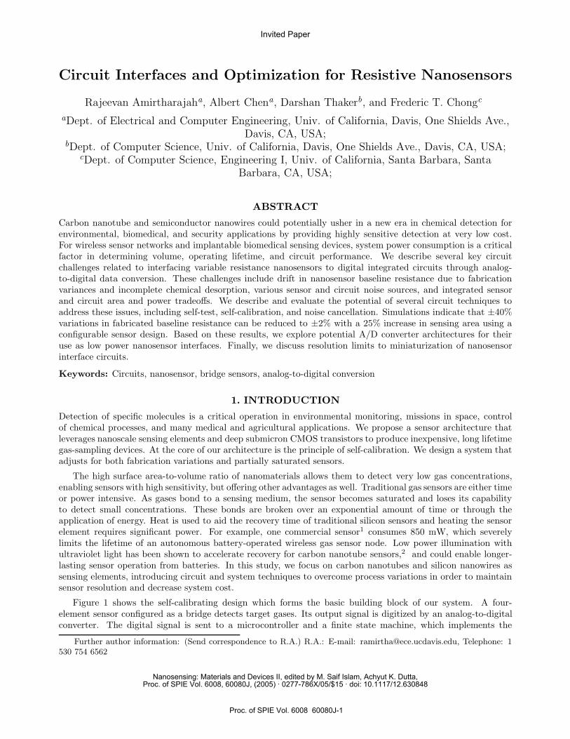
Figure 1 shows the self-calibrating design which forms the basic building block of our system. A four-element sensor configured as a bridge detects target gases. Its output signal is digitized by an analog-to-digitalconverter. The digital signal is sent to a microcontroller and a finite state machine, which implements the
Further author information: (Send correspondence to R.A.) R.A.: E-mail: [email protected], Telephone: 1530 754 6562
Invited Paper
Nanosensing: Materials and Devices II, edited by M. Saif Islam, Achyut K. Dutta,Proc. of SPIE Vol. 6008, 60080J, (2005) · 0277-786X/05/$15 · doi: 10.1117/12.630848
Proc. of SPIE Vol. 6008 60080J-1
SWNTor
SiNW
SWNTor
SiNW
SWNTor
SiNW
SWNTor
SiNW
Bridge Sensor
A/D Converter
ConfigurationFSM
to Microcontroller
Figure 1. Self-calibrating sensor block diagram.
sensor configuration and calibration. This calibration capability allows us to maintain gas sensing accuracyin parts-per-billion (versus the 10 parts-per-million available from conventional sensors) in the face of largenanoscale fabrication variations. This same calibration capability allows us to dynamically redefine the baselinefor minimum measurable gas concentrations as the sensor saturates. We use this moving baseline to iterativelyadapt to environmental gas levels, detecting saturated readings, and enabling the potential application of energyto move the sensor array out of saturation. Furthermore, we exploit the low bandwidth requirements of gassensing applications to develop interface circuits with very low power consumption. These circuits occupymodest area in deep submicron CMOS while still maintaining sensor resolution and thus help reduce system costas well as power.
In the next section, we further describe the characteristics of both carbon nanotubes and silicon nanowires forgas sensing. This is followed, in Section 3, by a discussion of the critical issues in gas sensor element design andpresents the self-calibrating building block for our architecture. Section 4 discusses the design of low power A/Dconverters targeting gas sensors and explores the circuit limits to gas detection for a minimal power interfacecircuit. We conclude with a discussion of open issues and future work and the impact of self-calibrating nanoscalearrays on broad areas of sensing.
2. SENSOR MATERIALS AND OPERATION
2.1. Carbon Nanotubes
Single dimensional, thin, hollow cylinders of carbon were first discovered in 1993 by groups at NEC and IBM.Single Walled Carbon Nanotubes (SWNTs), as they are called, have captured the imagination of researchers inphysics, chemistry and the material sciences. SWNTs have many remarkable properties, of which the electricalproperties are of interest to us. Armchair SWNTs display metallic properties while zigzag SWNTs tend to behaveas semiconductors.
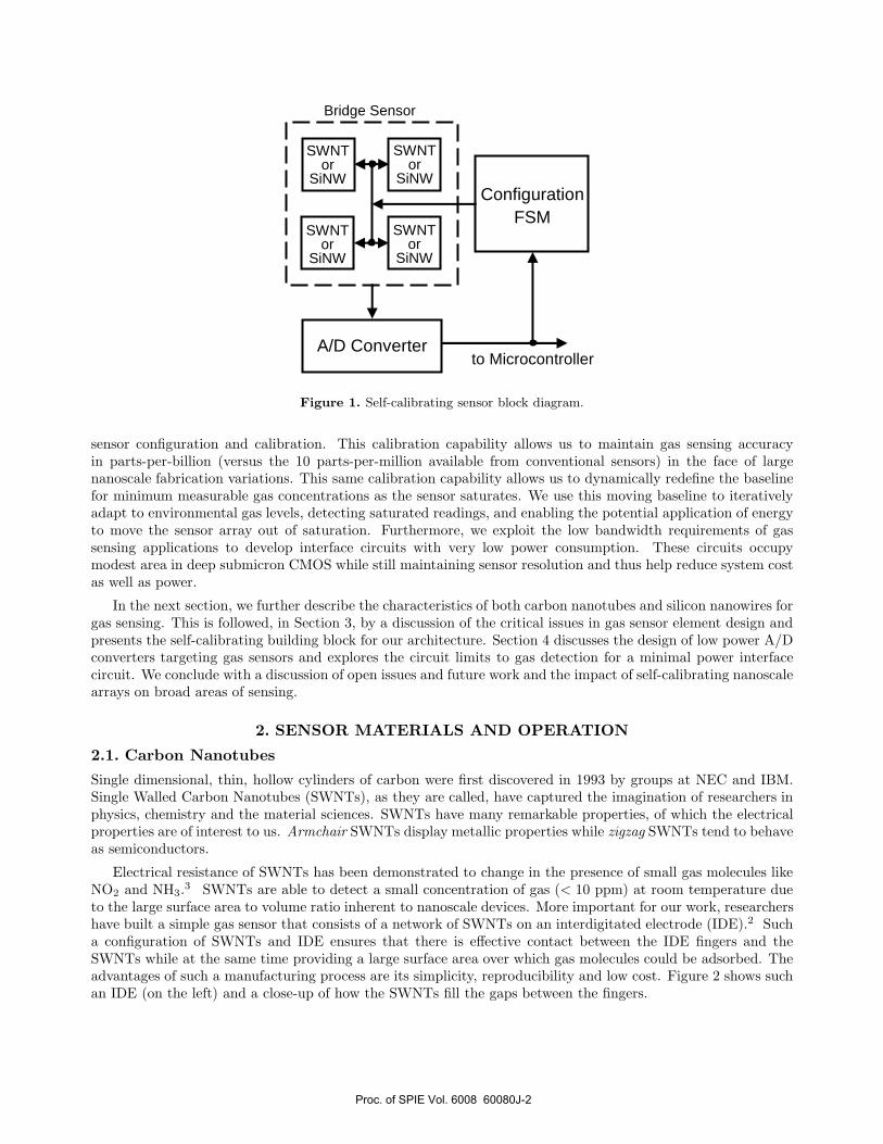
Electrical resistance of SWNTs has been demonstrated to change in the presence of small gas molecules likeNO2 and NH3.3 SWNTs are able to detect a small concentration of gas (< 10 ppm) at room temperature dueto the large surface area to volume ratio inherent to nanoscale devices. More important for our work, researchershave built a simple gas sensor that consists of a network of SWNTs on an interdigitated electrode (IDE).2 Sucha configuration of SWNTs and IDE ensures that there is effective contact between the IDE fingers and theSWNTs while at the same time providing a large surface area over which gas molecules could be adsorbed. Theadvantages of such a manufacturing process are its simplicity, reproducibility and low cost. Figure 2 shows suchan IDE (on the left) and a close-up of how the SWNTs fill the gaps between the fingers.
Proc. of SPIE Vol. 6008 60080J-2
There are two limitations of the just-mentioned sensor that have to be addressed before such a device can beused in the field. The first limitation is that not all the SWNTs that are deposited on the IDE are semiconducting,some of them are metallic. This is because it is very difficult to obtain a sample that contains SWNTs of only onetype. To overcome such discrepancies in the nature of the SWNTs, we think of them as manufacturing defectsand then design an architecture that accounts for these defects. We propose a calibration technique that involvesusing redundancy to improve sensor accuracy. In short, we use more than one IDE sensor. The calibration ofour sensor is described in detail in Section 3.3.
Figure 2. An IDE-SWNT sensor. The image on the left is one IDE. On the right is a magnified view of one IDE fingershowing SWNTs in the gap between fingers. From Li.2
2.2. Silicon NanowiresSemiconductor nanowires have also shown similar promise as molecular sensing devices. Lieber et al.4 haveshown chemical and biological sensing using individual CVD-grown Si nanowires, detecting simple metal ionsand proteins. A Si nanowire ChemFET was also reported to be highly sensitive to prostate-specific antigens.5
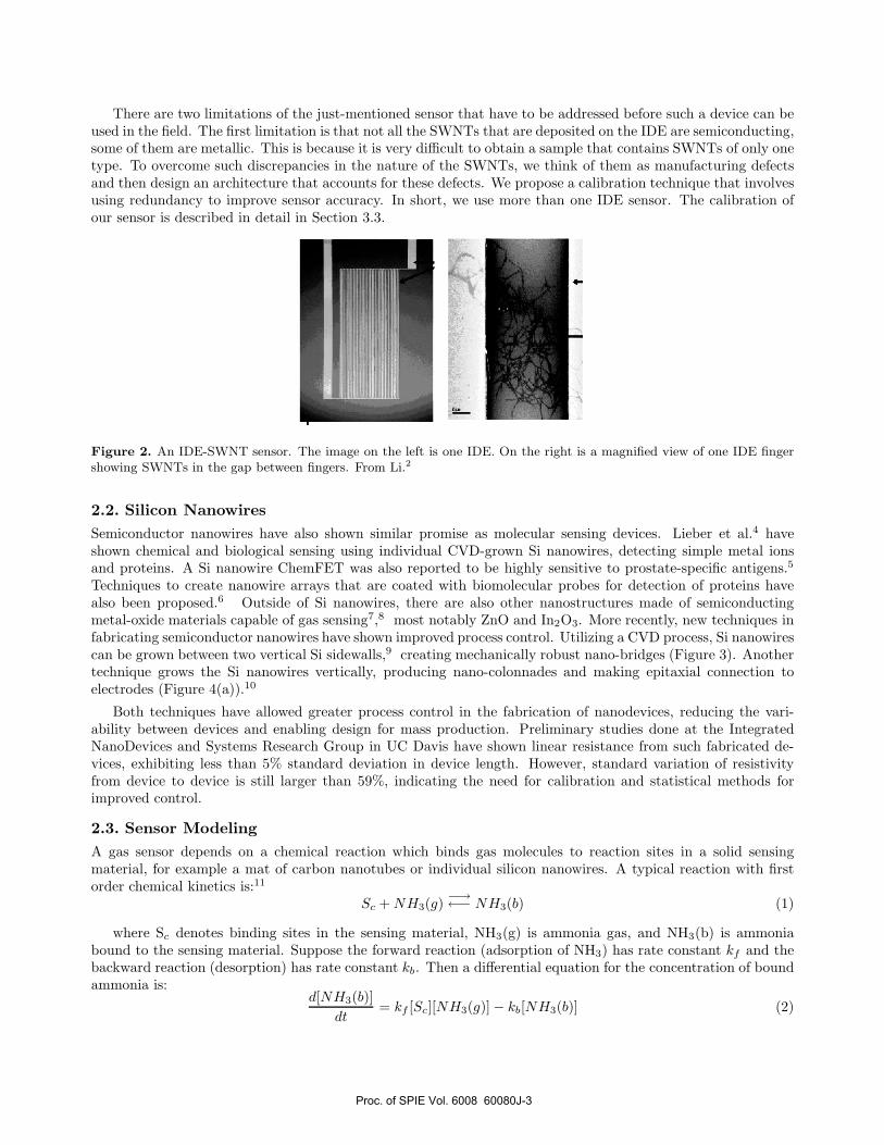
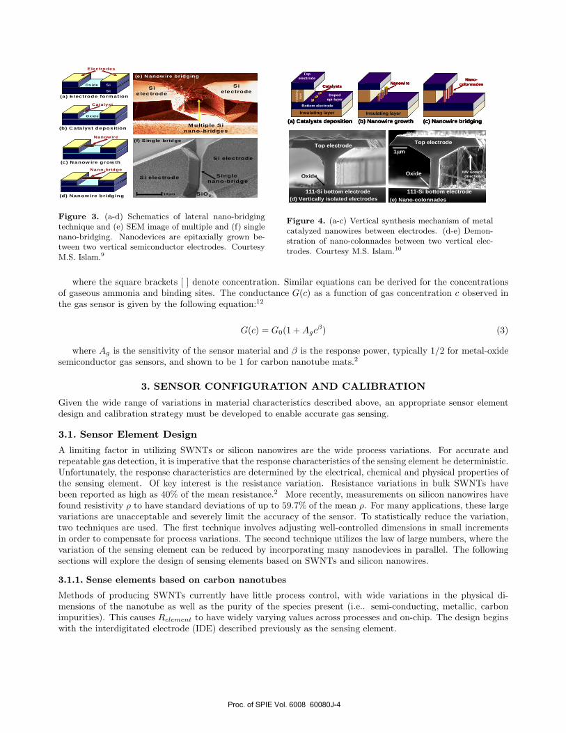
Techniques to create nanowire arrays that are coated with biomolecular probes for detection of proteins havealso been proposed.6 Outside of Si nanowires, there are also other nanostructures made of semiconductingmetal-oxide materials capable of gas sensing7,8 most notably ZnO and In2O3. More recently, new techniques infabricating semiconductor nanowires have shown improved process control. Utilizing a CVD process, Si nanowirescan be grown between two vertical Si sidewalls,9 creating mechanically robust nano-bridges (Figure 3). Anothertechnique grows the Si nanowires vertically, producing nano-colonnades and making epitaxial connection toelectrodes (Figure 4(a)).10
Both techniques have allowed greater process control in the fabrication of nanodevices, reducing the vari-ability between devices and enabling design for mass production. Preliminary studies done at the IntegratedNanoDevices and Systems Research Group in UC Davis have shown linear resistance from such fabricated de-vices, exhibiting less than 5% standard deviation in device length. However, standard variation of resistivityfrom device to device is still larger than 59%, indicating the need for calibration and statistical methods forimproved control.
2.3. Sensor ModelingA gas sensor depends on a chemical reaction which binds gas molecules to reaction sites in a solid sensingmaterial, for example a mat of carbon nanotubes or individual silicon nanowires. A typical reaction with firstorder chemical kinetics is:11
Sc + NH3(g) −→←− NH3(b) (1)
where Sc denotes binding sites in the sensing material, NH3(g) is ammonia gas, and NH3(b) is ammoniabound to the sensing material. Suppose the forward reaction (adsorption of NH3) has rate constant kf and thebackward reaction (desorption) has rate constant kb. Then a differential equation for the concentration of boundammonia is:
d[NH3(b)]dt
= kf [Sc][NH3(g)]− kb[NH3(b)] (2)
Proc. of SPIE Vol. 6008 60080J-3
- I WT ww
(c) N anow ire grow th
Nanow ire
(d) Nanow ire bridging
Nan o-brid ge
(b) C atalyst deposition
Oxide
Catalyst
(a) Electrode formation
Oxide S i
S i
Oxide S i
S i
E le ctro des
Si electrode
Si electrode
Single nano-bridge
SiO 210µm
Si electrode
Si electrode
Single nano-bridge
SiO 210µm
(e) N anow ire bridging
(f) S ingle bridge
M ultip le Sinano-bridges
Sielectrode
Sie lectrode
Figure 3. (a-d) Schematics of lateral nano-bridgingtechnique and (e) SEM image of multiple and (f) singlenano-bridging. Nanodevices are epitaxially grown be-tween two vertical semiconductor electrodes. CourtesyM.S. Islam.9
Top electrode
111-Si bottom electrode
Oxide
Top electrode
111-Si bottom electrode
Oxide
1µm
NW Growth direction
(a) Catalysts deposition
CatalystsNanowire
Nano-colonnades
Doped epi-layer
Bottom electrode
Top electrode
Insu
latin
g la
yer
(b) Nanowire growth
Insulating layer Insulating layer
(c) Nanowire bridging
(d) Vertically isolated electrodes (e) Nano-colonnades
Top electrode
111-Si bottom electrode
Oxide
Top electrode
111-Si bottom electrode
Oxide
1µm
NW Growth direction
(a) Catalysts deposition
CatalystsNanowire
Nano-colonnades
Doped epi-layer
Bottom electrode
Top electrode
Insu
latin
g la
yer
(b) Nanowire growth
Insulating layer Insulating layer
(c) Nanowire bridging(a) Catalysts deposition
CatalystsNanowire
Nano-colonnades
Doped epi-layer
Bottom electrode
Top electrode
Insu
latin
g la
yer
(b) Nanowire growth
Insulating layer Insulating layer
(c) Nanowire bridging
(d) Vertically isolated electrodes (e) Nano-colonnades
Figure 4. (a-c) Vertical synthesis mechanism of metalcatalyzed nanowires between electrodes. (d-e) Demon-stration of nano-colonnades between two vertical elec-trodes. Courtesy M.S. Islam.10
where the square brackets [ ] denote concentration. Similar equations can be derived for the concentrationsof gaseous ammonia and binding sites. The conductance G(c) as a function of gas concentration c observed inthe gas sensor is given by the following equation:12
G(c) = G0(1 + Agcβ) (3)
where Ag is the sensitivity of the sensor material and β is the response power, typically 1/2 for metal-oxidesemiconductor gas sensors, and shown to be 1 for carbon nanotube mats.2
3. SENSOR CONFIGURATION AND CALIBRATION
Given the wide range of variations in material characteristics described above, an appropriate sensor elementdesign and calibration strategy must be developed to enable accurate gas sensing.
3.1. Sensor Element Design
A limiting factor in utilizing SWNTs or silicon nanowires are the wide process variations. For accurate andrepeatable gas detection, it is imperative that the response characteristics of the sensing element be deterministic.Unfortunately, the response characteristics are determined by the electrical, chemical and physical properties ofthe sensing element. Of key interest is the resistance variation. Resistance variations in bulk SWNTs havebeen reported as high as 40% of the mean resistance.2 More recently, measurements on silicon nanowires havefound resistivity ρ to have standard deviations of up to 59.7% of the mean ρ. For many applications, these largevariations are unacceptable and severely limit the accuracy of the sensor. To statistically reduce the variation,two techniques are used. The first technique involves adjusting well-controlled dimensions in small incrementsin order to compensate for process variations. The second technique utilizes the law of large numbers, where thevariation of the sensing element can be reduced by incorporating many nanodevices in parallel. The followingsections will explore the design of sensing elements based on SWNTs and silicon nanowires.
3.1.1. Sense elements based on carbon nanotubes
Methods of producing SWNTs currently have little process control, with wide variations in the physical di-mensions of the nanotube as well as the purity of the species present (i.e.. semi-conducting, metallic, carbonimpurities). This causes Relement to have widely varying values across processes and on-chip. The design beginswith the interdigitated electrode (IDE) described previously as the sensing element.
4
Proc. of SPIE Vol. 6008 60080J-4
Ssuspend calibnane
suspend oslibraus
Figure a Figure
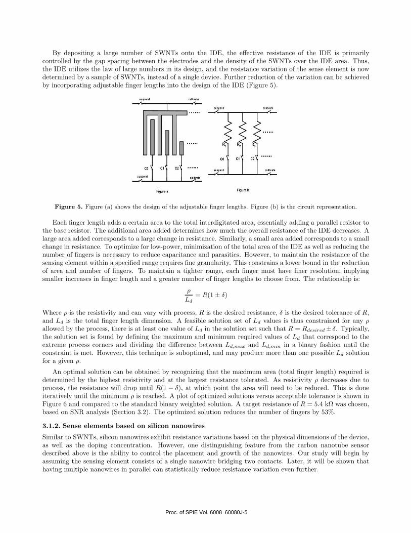
By depositing a large number of SWNTs onto the IDE, the effective resistance of the IDE is primarilycontrolled by the gap spacing between the electrodes and the density of the SWNTs over the IDE area. Thus,the IDE utilizes the law of large numbers in its design, and the resistance variation of the sense element is nowdetermined by a sample of SWNTs, instead of a single device. Further reduction of the variation can be achievedby incorporating adjustable finger lengths into the design of the IDE (Figure 5).
Figure 5. Figure (a) shows the design of the adjustable finger lengths. Figure (b) is the circuit representation.
Each finger length adds a certain area to the total interdigitated area, essentially adding a parallel resistor tothe base resistor. The additional area added determines how much the overall resistance of the IDE decreases. Alarge area added corresponds to a large change in resistance. Similarly, a small area added corresponds to a smallchange in resistance. To optimize for low-power, minimization of the total area of the IDE as well as reducing thenumber of fingers is necessary to reduce capacitance and parasitics. However, to maintain the resistance of thesensing element within a specified range requires fine granularity. This constrains a lower bound in the reductionof area and number of fingers. To maintain a tighter range, each finger must have finer resolution, implyingsmaller increases in finger length and a greater number of finger lengths to choose from. The relationship is:
ρ
Ld= R(1± δ)
Where ρ is the resistivity and can vary with process, R is the desired resistance, δ is the desired tolerance of R,and Ld is the total finger length dimension. A feasible solution set of Ld values is thus constrained for any ρallowed by the process, there is at least one value of Ld in the solution set such that R = Rdesired± δ. Typically,the solution set is found by defining the maximum and minimum required values of Ld that correspond to theextreme process corners and dividing the difference between Ld,max and Ld,min in a binary fashion until theconstraint is met. However, this technique is suboptimal, and may produce more than one possible Ld solutionfor a given ρ.
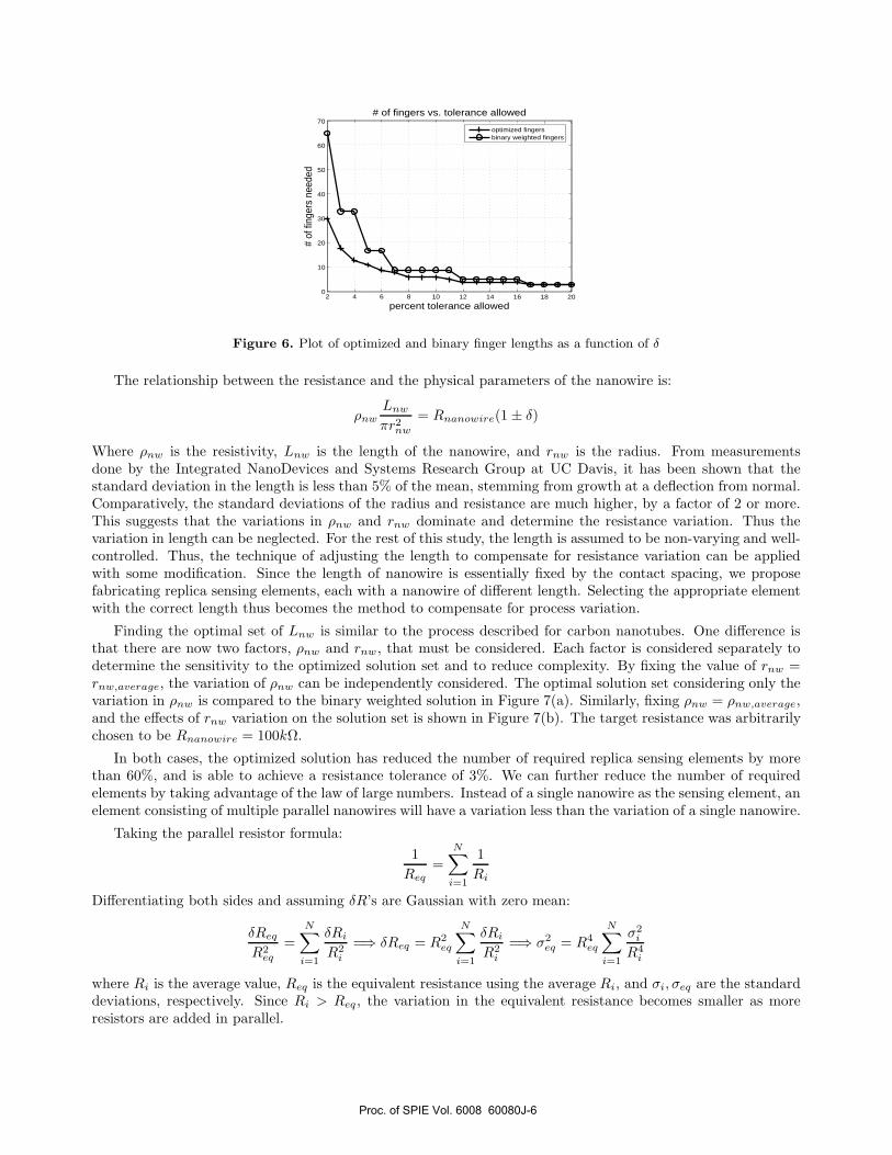
An optimal solution can be obtained by recognizing that the maximum area (total finger length) required isdetermined by the highest resistivity and at the largest resistance tolerated. As resistivity ρ decreases due toprocess, the resistance will drop until R(1 − δ), at which point the area will need to be reduced. This is doneiteratively until the minimum ρ is reached. A plot of optimized solutions versus acceptable tolerance is shown inFigure 6 and compared to the standard binary weighted solution. A target resistance of R = 5.4 kΩ was chosen,based on SNR analysis (Section 3.2). The optimized solution reduces the number of fingers by 53%.
3.1.2. Sense elements based on silicon nanowires
Similar to SWNTs, silicon nanowires exhibit resistance variations based on the physical dimensions of the device,as well as the doping concentration. However, one distinguishing feature from the carbon nanotube sensordescribed above is the ability to control the placement and growth of the nanowires. Our study will begin byassuming the sensing element consists of a single nanowire bridging two contacts. Later, it will be shown thathaving multiple nanowires in parallel can statistically reduce resistance variation even further.
Proc. of SPIE Vol. 6008 60080J-5
2 4 6 8 10 12 14 16 18 200
10
20
30
40
50
60
70
percent tolerance allowed#
of fi
nger
s ne
eded
# of fingers vs. tolerance allowed
optimized fingersbinary weighted fingers
Figure 6. Plot of optimized and binary finger lengths as a function of δ
The relationship between the resistance and the physical parameters of the nanowire is:
ρnwLnw
πr2nw
= Rnanowire(1 ± δ)
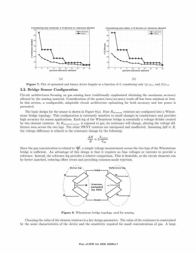
Where ρnw is the resistivity, Lnw is the length of the nanowire, and rnw is the radius. From measurementsdone by the Integrated NanoDevices and Systems Research Group at UC Davis, it has been shown that thestandard deviation in the length is less than 5% of the mean, stemming from growth at a deflection from normal.Comparatively, the standard deviations of the radius and resistance are much higher, by a factor of 2 or more.This suggests that the variations in ρnw and rnw dominate and determine the resistance variation. Thus thevariation in length can be neglected. For the rest of this study, the length is assumed to be non-varying and well-controlled. Thus, the technique of adjusting the length to compensate for resistance variation can be appliedwith some modification. Since the length of nanowire is essentially fixed by the contact spacing, we proposefabricating replica sensing elements, each with a nanowire of different length. Selecting the appropriate elementwith the correct length thus becomes the method to compensate for process variation.
Finding the optimal set of Lnw is similar to the process described for carbon nanotubes. One difference isthat there are now two factors, ρnw and rnw , that must be considered. Each factor is considered separately todetermine the sensitivity to the optimized solution set and to reduce complexity. By fixing the value of rnw =rnw,average, the variation of ρnw can be independently considered. The optimal solution set considering only thevariation in ρnw is compared to the binary weighted solution in Figure 7(a). Similarly, fixing ρnw = ρnw,average,and the effects of rnw variation on the solution set is shown in Figure 7(b). The target resistance was arbitrarilychosen to be Rnanowire = 100kΩ.
In both cases, the optimized solution has reduced the number of required replica sensing elements by morethan 60%, and is able to achieve a resistance tolerance of 3%. We can further reduce the number of requiredelements by taking advantage of the law of large numbers. Instead of a single nanowire as the sensing element, anelement consisting of multiple parallel nanowires will have a variation less than the variation of a single nanowire.
Taking the parallel resistor formula:1
Req=
N∑
i=1
1Ri
Differentiating both sides and assuming δR’s are Gaussian with zero mean:
δReq
R2eq
=N∑
i=1
δRi
R2i
=⇒ δReq = R2eq
N∑
i=1
δRi
R2i
=⇒ σ2eq = R4
eq
N∑
i=1
σ2i
R4i
where Ri is the average value, Req is the equivalent resistance using the average Ri, and σi, σeq are the standarddeviations, respectively. Since Ri > Req , the variation in the equivalent resistance becomes smaller as moreresistors are added in parallel.
Proc. of SPIE Vol. 6008 60080J-6
2 4 6 8 10 12 14 16 18 200
10
20
30
40
50
60
70
percent tolerance allowed
# of
dev
ices
nee
ded
Considering only resistivity, # of devices vs. tolerance allowed
optimizedbinary
(a)
2 4 6 8 10 12 14 16 18 200
10
20
30
40
50
60
70
percent tolerance allowed
# of
dev
ices
Considering only radius, # of devices vs. tolerance allowed
optimizedbinary
(b)
Figure 7. Plot of optimized and binary device lengths as a function of δ, considering only (a) ρnw and (b)rnw
3.2. Bridge Sensor Configuration
Circuit architectures focusing on gas sensing have traditionally emphasized obtaining the maximum accuracyallowed by the sensing material. Consideration of the power/area/accuracy trade-off has been minimal at best.In this section, a configurable, adaptable circuit architecture optimizing for both accuracy and low power ispresented.
The basic design for the sensor is shown in Figure 8(a). Four Relement resistors are configured into a Wheat-stone bridge topology. This configuration is extremely sensitive to small changes in conductance and provideshigh accuracy for sensor applications. Each leg of the Wheatstone bridge is essentially a voltage divider createdby two element resistors. As Relement,sense is exposed to gas, its resistance will change, altering the voltage dif-ference seen across the two legs. The other SWNT resistors are unexposed and unaffected. Assuming ∆R R,the voltage difference is related to the resistance change by the following:
∆R
R≈ 2
Vsense
Vdd
Since the gas concentration is related to ∆RR , a simple voltage measurement across the two legs of the Wheatstone
bridge is sufficient. An advantage of this design is that it requires no bias voltages or currents to provide areference. Instead, the reference leg provides a relative comparison. This is desirable, as the circuit elements canbe better matched, reducing offset errors and providing common-mode rejection.
Vdd
Gnd
+ -Vsense,sampledby ADC
Relement,leg1
Relement,sensor
Relement,leg2
Relement,leg3
Sense leg Reference leg
Figure 8. Wheatstone bridge topology used for sensing.
Choosing the value of the element resistors is a key design parameter. The value of the resistance is constrainedby the noise characteristics of the device and the sensitivity required for small concentrations of gas. A large
Proc. of SPIE Vol. 6008 60080J-7
a) Absolute ReferenceCalibration Mode
goldenreference
Relement
1k reference
1k reference
Vdd
Vdd
Vref
Vcal
Calibrationinstructions
u1
x2
x1 * / *
Analog to DigitalConverter
(a)
b) Relative ReferenceCalibration Mode
Relement, sensor
Vdd
Vdd
Vref
Vcal
Calibrationinstructions
Relement, leg1
Relement, leg2
Relement, leg3
u1
x2
x1 * / *
Analog to DigitalConverter
(b)
c) OffsetCalibration Mode
Relement, sensor
Vdd
Vdd
Vref
Vcal
OffsetCalibrationinstructions
Relement, leg1
Relement, leg2
Relement, leg3
u1
x2
x1 * / *
Analog to DigitalConverter
(c)
d) SensingMode
Relement, sensor
Vdd
Vdd
Vref
Vcal
Digital Outputto
Processor
Relement, leg1
Relement, leg2
Relement, leg3
u1
x2
x1 * / *
Analog to DigitalConverter
(d)
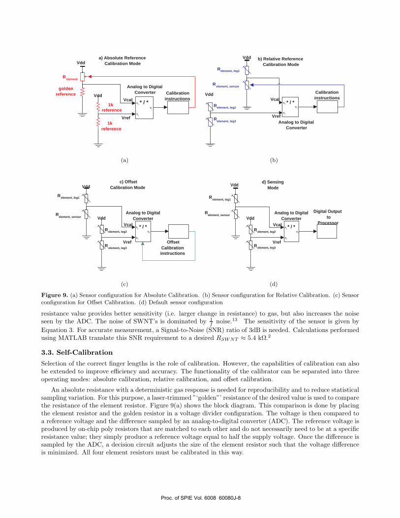
Figure 9. (a) Sensor configuration for Absolute Calibration. (b) Sensor configuration for Relative Calibration. (c) Sensorconfiguration for Offset Calibration. (d) Default sensor configuration
resistance value provides better sensitivity (i.e. larger change in resistance) to gas, but also increases the noiseseen by the ADC. The noise of SWNT’s is dominated by 1
f noise.13 The sensitivity of the sensor is given byEquation 3. For accurate measurement, a Signal-to-Noise (SNR) ratio of 3dB is needed. Calculations performedusing MATLAB translate this SNR requirement to a desired RSWNT ≈ 5.4 kΩ.2
3.3. Self-Calibration
Selection of the correct finger lengths is the role of calibration. However, the capabilities of calibration can alsobe extended to improve efficiency and accuracy. The functionality of the calibrator can be separated into threeoperating modes: absolute calibration, relative calibration, and offset calibration.
An absolute resistance with a deterministic gas response is needed for reproducibility and to reduce statisticalsampling variation. For this purpose, a laser-trimmed ”‘golden”’ resistance of the desired value is used to comparethe resistance of the element resistor. Figure 9(a) shows the block diagram. This comparison is done by placingthe element resistor and the golden resistor in a voltage divider configuration. The voltage is then compared toa reference voltage and the difference sampled by an analog-to-digital converter (ADC). The reference voltage isproduced by on-chip poly resistors that are matched to each other and do not necessarily need to be at a specificresistance value; they simply produce a reference voltage equal to half the supply voltage. Once the difference issampled by the ADC, a decision circuit adjusts the size of the element resistor such that the voltage differenceis minimized. All four element resistors must be calibrated in this way.
Proc. of SPIE Vol. 6008 60080J-8
Once the sensor is in operation, the element resistors may experience changes in resistance due to processdrift or electrical stress. In this case, the calibrator is utilized to improve the common-mode rejection betweenthe two legs of the Wheatstone bridge. In Figure 9(b), the ADC is sampling the voltage difference betweenthe two legs of the Wheatstone bridge. This difference is then used to adjust Relement,sensor to reflect the newbaseline resistance. Only Relement,sensor needs to be adjusted, as Relement,leg has not been exposed to gas andprovides a good indicator to process drift.
The calibration technique can also be used to improve accuracy dynamically. The absolute and relativecalibration assumes that the sensor is idle and has sufficiently recovered to return to its static base state.However, during sensing operation, the sensor can gain further improvement by dynamically normalizing thebase resistance and measuring the difference between future values and the new ”‘recalibrated”’ base resistance.This is shown in Figure 9(c). In this topology, the ADC samples the difference between the sensing leg and thereference leg. This offset is stored and used to adjust the ADC so that all subsequent samples are compared tothis common offset. In a sense, the ADC renormalizes itself and gains dynamic range. Another usage of offsetcalibration is to achieve finer resolution than what absolute or relative calibration allows. For example, afterabsolute or relative calibration, there may still be some small difference in the absolute and relative values of theelement resistors. This difference directly limits the sensitivity of the ADC. Since this difference is DC common,the system can adjust and remove this DC offset, should further accuracy be desired. This is similar to filteringout the common-mode noise.
Determination of what type of calibration is needed can be shown in Figure 10. If the system is presentlyaccurate enough, then no calibration is needed. If the system is not accurate enough by a user-defined setting,then the system examines how far off the current accuracy is compared to the desired accuracy. If the accuracyis off by more than 2 LSBdesired, then the system will initiate an absolute calibration. If the accuracy is off byless than 2 LSBdesired, then the system will initiate a relative calibration. After each stage of calibration, thesystem determines whether additional calibration is needed or not. The 2 LSBdesired is determined by assumingthe Relement,sensor is off by more than 1%. This roughly translates to a mismatch offset voltage of 5 mV for a 1 Vsupply. This is roughly 1 LSBmin of an 8-bit ADC. To have the desired accuracy and reliablity, the ADC must beable to distinguish at least 1
2 LSBdesired. The system validates its accuracy by measuring the difference betweenthe sensing leg and the reference leg. If the difference is larger than 1
2 LSBdesired, then additional calibration isrequired. If after going through absolute calibration, relative calibration and offset calibration the system stillcannot resolve the accuracy setting, then the only option is to reset the accuracy setting or wait until conditionsallow the desired accuracy.
4. CIRCUIT INTERFACE
The integration of nanotube and nanowire sensors with CMOS transistors offers further opportunities in in-telligent sensor design beyond self-calibration and compensation for process variations described in precedingsections. We are exploring alternative topologies for analog-to-digital conversion that exploit the low bandwidthnature of gas sensor signals to decrease system power consumption and relax transistor matching requirements.Both issues are significant challenges as CMOS scales into the deep submicron region.
4.1. Voltage Mode A/D ConverterA highly accurate A/D converter (ADC) design is required to detect gas concentrations as low as 1 ppb. Forexample, spanning a dynamic range for concentration from 1 ppb to 10 ppm requires a 16 bit converter. Currentdesign techniques have allowed ADCs to achieve precision as great as 24 bits of resolution. However, mostof these techniques do not lend themselves easily to low power, low energy adaptations. Recently, an ADCdesign proposed by Scott, et. al.14 has set the standard in terms of energy efficiency per bit. However, itsmaximum precision of 8 bits limits the lowest detectable gas concentration and provides insufficient resolutionfor postprocessing techniques such as digital filtering. We are exploring techniques to increase ADC resolutionto 16 bits while minimizing energy consumption.
To minimize energy during system operation, the ADC must scale energy with accuracy, allowing the userto exploit the energy/accuracy tradeoff. This implies a variable precision design, while minimizing power at allprecisions. Two approaches widely considered for low energy applications are successive approximation ADCs
Proc. of SPIE Vol. 6008 60080J-9

Calibration FlowDiagram
CalibrationStart/End
UV reset
AbsoluteCalibration
RelativeCalibration
OffsetCalibration
Report Offset or Accuracy
Offset Calibrationrequested
Offset > 2 LSB desired ,inaccurate
Accurateoffset < 0.5 LSB desired
0.5 LSB desired < Offset < 2 LSB desired ,requires Relative Calibration
Accurateoffset < 0.5 LSB desired
Base resistance changed,need to recalibrate
0.5 LSB desired < Offset < 2 LSB desired,need additional calibration
0.5 LSB desired < Offset < 2 LSB desired ,requires further calibration
Accurateoffset < 0.5 LSB desired
UV Reset requested
Offset > 2 LSB desired, still inaccurate
Figure 10. Calibration State Flow
and algorithmic ADCs. Both approaches scale precision with energy, however the successive approximation ADCallows initialization of the internal state. This allows the ADC to begin its search at an estimated value, thusreducing convergence time and energy consumption and makes successive approximation attractive for sensorapplications.
Charge Redistribution ADC One implementation of successive approximation is to sample the input ontoa capacitor array. The capacitors are disconnected from the input and a subset are connected to a referencevoltage Vref . There is no low impedance path for the capacitors to discharge, so the charge redistributes itself onthe new equivalent capacitance. The resulting output voltage Vout is: Vin − Vref ∗ Cswitch
Ctotalwhere Vin is the input
voltage, Cswitch are the capacitors that are sourced to Vref and Ctotal is the entire capacitor array. By sizingthe capacitor array to be binary weighted and selecting Cswitch so that Voutput = 0, we can compute the inputvoltage as a binary code normalized to Vref . The main drawback in successive approximation ADCs is the arearequired in the capacitor array. To make successive approximation ADCs high precision, large unit capacitorsare needed to minimize noise (proportional to kT
C ) and the effects of process variation. Each bit increase inprecision requires a 2X increase in capacitor area, corresponding to an exponential increase in energy consumed.The energy consumed in charging the capacitor array in a 16-bit ADC is 256 times greater than for an 8-bitADC.
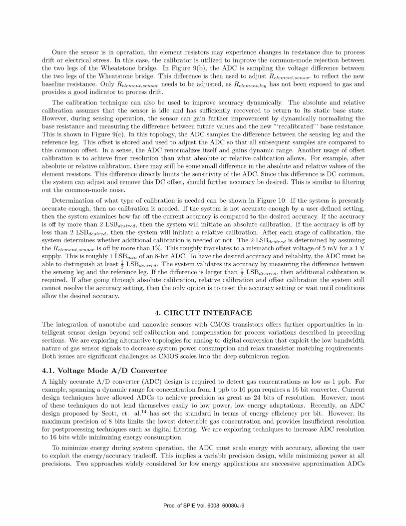
Flash + Charge Redistribution ADC To reduce energy, we are developing a flash ADC to compute themost significant bits (MSBs) of the ADC output. Typically, flash ADCs use resistor strings and are utilizedfor their speed, not low power. By replacing the resistor string with a capacitor string, we eliminate staticpower, and are only concerned with the dynamic charging of the capacitors and the power consumed by thecomparator. By reusing the capacitor array from the successive approximation ADC, we can also minimize area.Calculations show that the optimal design for a 16 bit ADC which combines successive approximation and flasharchitectures uses the flash portion to compute the first 5 MSB bits and the remaining 11 bits are computed bysuccessive approximation. Figure 11(a)-(b) shows the block diagram of the proposed design. The flash converteris implemented by a second switching network.
Logarithmic ADC Sensing a wide dynamic range of gas concentrations demands a large number of ADCoutput bits. An alternative is to use a logarithmic mapping ADC which converts a wide linear dynamic range
Proc. of SPIE Vol. 6008 60080J-10
—)F
-)I°
)-
)--(
T
l 0 C,
16 bit Combination FlashSuccesive Approximation ADC
Ce ntre I
V.,
16 bit code
Code
(a) (b)
Figure 11. (a) Flash ADC architecture. (b) Flash + capacitor array successive approximation ADC architecture.
M0
M3M1 M2
M5 M4
M9 M7 M6 M8
n0 n1
Out Out
vsense vref
clk
clk
(a)
Comparator Offset Voltage
0.000
0.500
1.000
1.500
2.000
2.500
3.000
3.500
4.000
0.0 0.5 1.0 1.5 2.0 2.5 3.0
Device Mismatch (σ)
v os
(mV
)
CalculatedSimulated
(b)
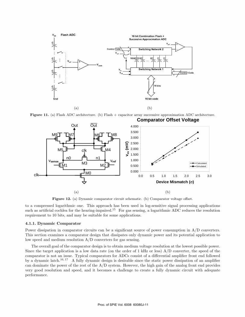
Figure 12. (a) Dynamic comparator circuit schematic. (b) Comparator voltage offset.
to a compressed logarithmic one. This approach has been used in log-sensitive signal processing applicationssuch as artificial cochlea for the hearing-impaired.15 For gas sensing, a logarithmic ADC reduces the resolutionrequirement to 10 bits, and may be suitable for some applications.
4.1.1. Dynamic Comparator
Power dissipation in comparator circuits can be a significant source of power consumption in A/D converters.This section examines a comparator design that dissipates only dynamic power and its potential application tolow speed and medium resolution A/D converters for gas sensing.
The overall goal of the comparator design is to obtain medium voltage resolution at the lowest possible power.Since the target application is a low data rate (on the order of 1 kHz or less) A/D converter, the speed of thecomparator is not an issue. Typical comparators for ADCs consist of a differential amplifier front end followedby a dynamic latch.16, 17 A fully dynamic design is desirable since the static power dissipation of an amplifiercan dominate the power of the rest of the A/D system. However, the high gain of the analog front end providesvery good resolution and speed, and it becomes a challenge to create a fully dynamic circuit with adequateperformance.
Proc. of SPIE Vol. 6008 60080J-11
Figure 12(a) shows a dynamic comparator. The circuit consists of a cross-coupled CMOS inverter pair(M4-M7), a matched differential input pair (M1 and M2), a set of precharge devices (M3 and M8-M9), and anevaluation device (M0). When the clock signal is low, PMOS transistors M8 and M9 are turned on and NMOStransistor M0 is cut off, thus pulling differential output nodes Out and Out high. This turns on devices M5and M4 and precharges circuit nodes n0 and n1. Transistor M3 equalizes the voltages between the two nodes.During the evaluate phase, clock goes high and devices M8 and M9 are cut off while M0 turns on. The voltagesat n0 and n1 start to decrease, and the rate at which they are discharged depends on the gate voltages Vsense
and Vref . Whichever node pulls down first engages the positive feedback in the cross-coupled inverters and pullsthe outputs to a final value (for example, Out = Vdd and Out = 0 if Vsense < Vref ).
Mismatch between devices M1 and M2 limits the smallest voltage difference Vsense−Vref which can be reliablydetermined by the comparator.18 Experimental data for a number of CMOS processes has shown that thresholdvoltage differences ∆VT and current factor differences ∆β, where β = µCoxW/L are the dominant sourcesof mismatch.19 These random differences are generally considered to be independent normally distributedrandom variables with variances inversely dependent on the device area WL, such that σ2(∆VT ) = A2
V T
WL and
σ2(∆β/β) = A2β
WL . Mismatch effects are typically expressed as an offset voltage vos, corresponding to the inputdifferential voltage Vsense − Vref which forces the outputs Out and Out to be equal. An equation for the offsetcan be derived assuming transistors M1 and M2 are operating in saturation:
vos = ∆VT +1
(gm/I0)
(∆β
β
)(4)
where the terms are as defined above. Since the dynamic comparator does not operate under a steady-state bias, this equation is not strictly applicable. However, the critical part of circuit operation occurs in theinitial discharge of nodes n0 and n1. For the Wheatstone bridge sensor, the common-mode voltage input tothe comparator is near Vdd/2, and so the transistors will be in saturation during the critical early part of theevaluation transient.
Using the sensitivity for the carbon nanotube mat sensor2 and the relation Vsense∼= Vdd(∆R/2R) ,we find
that to detect a minimum gas concentration of 200 ppb with a power supply Vdd = 1 V results in Vsense = 3.4mV. This minimum Vsense corresponds to a single LSB for the A/D converter and so we must choose W and Lfor devices M1 and M2 such that vos ≤ 1.7, or 1
2 LSB. Using data summarized in19, 20 to extrapolate values forAV T and Aβ for a 90nm CMOS technology and assuming that threshold voltage mismatch is the dominant effect,the required area is WL = 34.6µm2. This area is large in terms of the minimum device area in this technologybut is modest compared to the sensor area. We simulated the comparator pulldown paths with W = 17.3µmand L = 2.0µm for transistors M1 and M2 to determine the offset voltage for a range of device mismatch. Theresults are plotted in Figure 12(b), which shows that the calculated offsets are about 18% below the simulatedoffsets. This is reasonably accurate given that numerous effects due to nonzero source-bulk bias and the dynamicnature of the circuit were ignored in the simple calculation. The figure plots the offset as both ∆VT and ∆β/βare varied together from 0.5σ to 2.5σ and shows that the comparator resolution specification will be met over> 99% of mismatch.
4.2. Variable Conductance A/D Converter
An alternative to using charge redistribution is to exploit the variable conductance available through the recon-figurable sensor resistance. Rather than digitizing the voltage at the output of the Wheatstone bridge, the circuitcompares the conductance of the two legs directly by incorporating them into a comparator circuit as shownin Figure 13(a). The calibration setting Dsense configures the sense leg for optimum gas sensitivity. Duringconversion, a set of digital codes is applied to Dref , the comparator is evaluated using the clock signal for eachcode, and the output checked by digital logic to determine which code most closely corresponds to the sense legresistance. Previous implementations of this converter relied on accurate digital-to-analog conversion to convertconductance to voltage,21 but the gas sensing application does not require this since it relies on conductancedirectly. We are currently evaluating this converter architecture and comparing its performance in simulation tothe charge redistribution approach.
Proc. of SPIE Vol. 6008 60080J-12

M0
M3M1 M2
M5 M4
M9 M7 M6 M8
n0 n1
Out Out
Rsense Rref
Dsense Dref
clk
clk
(a)
Offset Resistance
0
5
10
15
20
25
30
35
40
45
0.0 0.5 1.0 1.5 2.0 2.5 3.0
Device Mismatch (σ)
Ro
s ( Ω
)
Calculated (W/L=8.7)
Simulated (W/L=8.7)
Calculated (W/L=2.2)
Simulated (W/L=2.2)
(b)
Figure 13. (a) Conductance-based successive approximation ADC architecture. (b) Comparator resistance offset.
The circuit in Figure 13(a) is very similar to the circuit in Figure 12(a), except that the resistances Rsense andRref ideally determine which node n0 and n1 discharges first. Consequently, any threshold voltage or currentfactor mismatch in the devices M1 and M2 will affect the total resistance of each pulldown path and limit thesmallest resistance difference which can be resolved by the comparator. Since the calibration settings Dsense
and Dref are digital codes, the gates of M1 and M2 will be driven to Vdd if they are turned on, so consequentlywe expect M1 and M2 to largely be in the linear (triode) region. Similar to voltage offset vos, we can derive a“resistance offset” ∆R which corresponds to the resistance difference that guarantees any threshold or currentfactor mismatch is overcome during comparator evaluation:
∆R ≈ −∆RM
(R
RM
)=
(∆β
β− ∆VT
Vgs − VT − Vds/2
)R (5)
where Vgs, VT , and Vds are the gate-source, threshold, and drain-source voltages and RM is the large signaldrain-source resistance of transistors M1 or M2, respectively, and R is the common-mode resistance betweenRsense and Rref . Note that the offset can be adjusted by varying the ratio between the transistor on resistancesand the sensor common-mode resistance, which yields a different tradeoff than the current biasing available tominimize the voltage offset.
Figure 13(b) plots the calculated and simulated resistance offsets versus device mismatch for pulldown switchesM1 and M2 having two alternative W/L ratios and the same area as the devices for the circuit in Figure 12(a).The simulated offset is typically better than the calculated offset for W/L = 8.7 and while the offset decreasesas W/L is decreased (RM is increased), it does not scale as quickly as Equation 5 indicates. This is likely dueto a number of competing effects including a nonzero source-bulk voltage, the implicit negative feedback of thesource resistance on the current through M1 and M2, and the dynamic nature of the circuit.
To detect a minimum concentration of 200 ppb results in a sensor resistance change of 36.7 Ω, and so theresistance offset due to comparator mismatch should be less than 18.3 Ω (1
2 LSB). For the same device area,Figure 13 shows that the resistance offset can be decreased significantly below this threshold for a wide range ofmismatch with an appropriate device sizing. The tradeoff is that by increasing RM , the evaluation time of thecomparator is also increased, but this is unlikely to limit performance in most gas sensing applications.
Proc. of SPIE Vol. 6008 60080J-13

5. FUTURE WORK
The ultimate goal of this project is to design and fabricate a manufacturable power-aware gas sensor, utilizingnanostructures for improved sensitivity and power efficiency. The previous sections describe some of the com-ponents and architectures needed to accomplish this goal. However, further investigation into three key areasare needed: 1) device characterization for improved modeling, 2) circuit investigations into power and accu-racy trade-offs and 3) system-level policies to govern sensor operation and adapt the sensor to meet end-userrequirements.
Further research into process improvements and characterization of nanodevices is crucial for their wide-spread adoption. In particular, better understanding of the causes in process variation will lead to improvedoptimization models. Current work in this area includes developing statistical methods of designing process-tolerant elements. Design of the sensor elements will also require improved gas response characterization of thesedevices, as the resistance and physical/chemical properties change with molecular absorption. In the extremecase, sensitivity is ultimately limited by the intrinsic noise of the devices. Noise characterization will affect bothcircuit implementation and architectural choice.
As MOSFET technology shrinks further into deep submicron, the increasing effects of device mismatch andreductions in supply voltage make it increasingly difficult to operate analog circuits. Indeed, the small-signalapproximations used in conventional analog circuit design (assuming constant current biases and operation inthe saturation region), are becoming less and less applicable. New design styles involving nonlinear and time-varying analog circuits such as the dynamic comparator discussed above are currently being investigated forpower reduction and increased input range. Subthreshold-based circuits are also another potential area wherethe power/accuracy trade-off could be better exploited. The vast numbers of transistors available providesopportunities for digital compensation of analog circuits and digital postprocessing of sensor data to improvesystem performance.
As the fundamental limitations of devices are approached, new system architectures must be developedthat compensate for wider statistical variation. Two techniques currently being explored are sensing elementredundancy and self-aware system design that can adapt to changing requirements through self-configuration.One example of the latter is the application of ultraviolet (UV) light to saturated sensing elements. It hasbeen shown that UV illumination can reduce the recovery time of SWNT sensors from 10 hours to 10 minutes,enabling increased sampling rate.2 It is also possible to use the application of UV light as a “quench” to quicklyreset the sensor back to baseline conditions for optimum sensitivity. Through a clever UV illumination policy, itis possible for a sensor to maintain a large dynamic range without compromising sensitivity.22 Hence, a systemcould overcome its current limitations through adaptation.
6. CONCLUSIONS
We have presented an integrated sensor and interface circuit design that focuses on the principle of self-calibrationto deliver dramatically improved gas sensing system performance from nanoscale sensor technology. Our designexploits the high sensitivity, high molecular selectivity, and low power of carbon nanotube and silicon nanowiresensing elements while addressing the challenges of manufacturing variation and mismatch in both the sensingelements and deep submicron CMOS transistors.
At the core of our design is the use of multiple sensor arrays to perform dynamic calibration. By optimizingthese sensor arrays, significant reductions in sensor variation can be obtained with minimal increase in sensorarea. We have demonstrated these reductions through analytical techniques applied to both carbon nanotubeand silicon nanowire variations. Furthermore, we have analyzed the potential of using dynamic comparatorcircuits as the sensor interface. These circuits offer drastically reduced power consumption by exploiting thelow data rate requirements for typical gas sensing applications to allow for long comparator evaluation times.In 90 nm CMOS, input device area on the order of 35 µm2 enables gas sensing resolution of 200 ppb for bothconventional and variable conductance A/D converters. Further improvements in resolution are available forlower conversion speed. The dramatic improvements in power efficiency and cost reductions achievable by thecombination of nanoscale sensing elements and CMOS circuits will create exciting new opportunities for sensorsin critical areas such as environmental science, chemistry, and public safety.
Proc. of SPIE Vol. 6008 60080J-14
ACKNOWLEDGMENTS
The authors would like to thank Prof. M. Saif Islam and Dr. Ibrahim Kimukin for allowing access to theirnanowire data and for their comments. This work is supported in part by a UC Davis Chancellor’s Fellowshipawarded to Fred Chong.
REFERENCES1. Figaro, “Ammonia gas sensor, part TGS826,” 2004.2. J. Li, Y. Lu, Q. Ye, M. Cinke, J. Han, and M.Meyyappan, “Carbon nanotube sensors for gas and organic
vapor detection,” NanoLetters 3 No. 7, pp. 929 – 933, 2003.3. J.Kong, N.Franklin, C.Zhou, M.Chapline, S.Peng, K.Cho, and H.Dai, “Nanotube molecular wires as chem-
ical sensors,” Science 287, 2000.4. Y. Cui, Q. Wei, H. Park, and C. M. Lieber, “Nanowire nanosensors for highly sensitive and selective detection
of biological and chemical species,” Science 293, p. 1289, 2001.5. “Commentary,” Science 300, p. 242, 2003.6. N. M. et al., “Ultrahigh density nanowire lattices and circuits,” Science 300, p. 112, 2001.7. Z. Wang, Nanowires and Nanobelts: Materials, Properties, and Devices, vol. II, pp. 3–16. Kluwer Academic
Publishers, Boston, MA, 2003.8. C. Li, D. Zhang, X. Liu, S. Han, T. Tang, J. Han, and C. W. Zhou, “In2o3 nanowires as gas sensors,”
Applied Physics Letters 82, pp. 1613–5, 2002.9. M. S. Islam, S. Sharma, T. I. Kamins, and R. S. Williams, “Ultrahigh-density silicon nanobridges formed
between two vertical silicon surfaces,” Nanotechnology 15, p. 5, 2004.10. M. S. Islam, T. I. Kamins, S. Sharma, and R. S. Williams in MRS Spring Meeting, (San Francisco), 2005.11. D. E. Williams and K. F. E. Pratt, “Resolving combustible gas mixtures using gas senstive resistors with
arrays of electrodes,” J. Chem. Soc. Faraday Trans. 92, issue 22, pp. 4497 – 4504, 1996.12. D. E. Williams and K. F. E. Pratt, “Theory of self-diagnostic sensor array devices using gas-sensitive
resistors,” J. Chem. Soc. Faraday Trans. 91, issue 13, pp. 1961 – 1966, 1995.13. P. G. Collins, M. S. Fuhrer, and A. Zettl, “1/f noise in carbon nanotubes,” Applied Physics Letters 76 No.
7, pp. 894 – 896, 2000.14. M. Scott, B. Boser, and K. Pister, “An ultra-low power adc for distributed sensor networks,” IEEE Journal
of Solid State Circuits 38 No 7, pp. 1123–1129, 2003.15. J.-J. Sit and R. Sarpeshkar, “A micropower logarithmic A/D with offset and temperature compensation,”
IEEE Journal of Solid-State Circuits 39, pp. 308–19, February 2004.16. T. Cho and P. Gray, “A 10-bit, 20-ms/s, 35-mw pipeline A/D converter,” in 1994 IEEE Custom Integrated
Circuits Conference, pp. 23.2.1–23.2.4, 1994.17. B. McCarroll, C. Sodini, and H.-S. Lee, “A high-speed CMOS comparator for use in an ADC,” IEEE Journal
of Solid-State Circuits SC-23, pp. 159–165, February 1988.18. P. R. Gray, P. J. Hurst, S. H. Lewis, and R. G. Meyer, Analysis and Design of Analog Integrated Circuits,
John Wiley & Sons, Inc., New York, 4th. ed., 2001.19. P. R. Kinget, “Device mismatch and tradeoffs in the design of analog circuits,” IEEE Journal of Solid-State
Circuits 40, pp. 1212–24, June 2005.20. J. T. Horstmann, U. Hilleringmann, and K. F. Goser, “Matching analysis of deposition defined 50-nm
MOSFETs,” IEEE Trans. on Electron Devices 45, pp. 299–306, January 1998.21. T. D. Simon, “Low power analog-to-digital converter.” US Patent 628867, September 2001.22. D. D. Thaker, A. Chen, R. Amirtharajah, and F. T. Chong, “On designing self-calibrating nanoscale sensors
that adaptively invest power for accuracy,” in Proc. of IEEE International Workshop on Design and Testof Defect-Tolerant Nanoscale Architectures (NANOARCH’05), May 2005.
Proc. of SPIE Vol. 6008 60080J-15