circuit layout techniques and tips (part i of vi) by ...bctill/uvatt/layout/acqt0524.pdf · circuit...
TRANSCRIPT
Circuit Layout Techniques And Tips (Part I of VI)by Bonnie C. Baker, Microchip Technology Inc.
The Art Of Laying Out Two-Layer BoardsIn this highly competitive, battery-powered marketplace, cost objectives usually dictatethat a designer use two-layer boards in the design. Although the multi-layer board (4-, 6-and 8-layers) allows the designer to build cleaner solutions in terms of size, noise andperformance, financial pressures force the engineer to rethink layout strategies with thetwo-layer board in mind. In this article we discuss the use or misuse of auto-routing, theconcept of current return paths with and without ground planes, and recommendations forcomponent placement where two-layer boards are concerned.
Pay Now Or Pay Later With The Auto-Router And Analog CircuitsIt is tempting to use the auto-router when designing printed circuit board (PCB.) Moreoften than not, a purely digital board, (especially if the signals are relatively slow, and thecircuit density is low) will work just fine. But as you try to lay out analog, mixed-signalor high-speed circuits with the auto-routing tool that is available with your layoutsoftware there may be some issues. The probability of creating serious circuitperformance problems is very real.
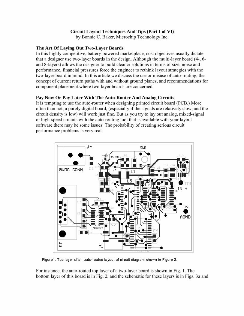
For instance, the auto-routed top layer of a two-layer board is shown in Fig. 1. Thebottom layer of this board is in Fig. 2, and the schematic for these layers is in Figs. 3a and

3b. For the layout of this mixed-signal circuit the devices were manually placed on theboard with careful thought to separating the digital and analog parts.
With this layout there are several areas of concern, but the most troubling issue is thegrounding strategy. If the ground traces are followed on the top layer, every device isconnected through traces on that layer. A second ground connection for every device usesthe bottom layer with vias at the far right-hand side of the board. The immediate red flagthat one should see when examining this layout strategy would be the existence of severalground loops. Additionally, the ground return paths on the bottom side are interruptedwith horizontal signal lines. The saving grace with this grounding scheme is that theanalog parts (MCP3202, 12-bit ADC and MCP4125, 2.5-V voltage reference) are at thefar right-hand side of the board. This placement ensures that digital ground signals do notpass under these analog chips.


The manual layout of the circuit shown in Figs. 3a and 3b is given in Figs. 4 and 5. Withthis manual layout a few general guidelines are followed to ensure positive results:• Use the ground plane as a current return path as much as possible.• Separate the analog ground plane from the digital ground plane with a break.• If interruptions from signal traces are required on the ground-plane side, make them
vertical to reduce the interference with the ground current return paths.• Place analog circuitry at the far-end of the board and digital circuitry closest to the
power connects. This reduces the effects of δi/δt from digital switching.
Note that with both of these two-layer boards there is a ground plane on the bottom. Thisis only done so that an engineer working on the board can quickly see the layout whentrouble shooting. This strategy is typically found with a manufacturer’s demo andevaluation boards. But, more typically, the ground plane is on the top of the board,thereby reducing electromagnetic interference (EMI.)


Current Return Paths With Or Without A Ground PlaneThe fundamental issues that should be considered when dealing with current return pathsare:• In the event that you are considering using traces for the ground connects on your
PCB, they should be designed to be as wide as possible. This is a good rule of thumb,but also understand that the thinnest width in your ground trace will be the effectivewidth of the trace from that point to the end, where the “end” is defined as the pointfurthest from the power connection.
• Ground loops should be avoided.• If no ground plane is available, star connection strategies should be used.
A graphical example of a star connection strategy is shown in Fig. 6.
With this type of approach the ground currents return to the power connectionindependently. You will note that in Fig. 6 all of the devices do not have their own returnpath. With U1 and U2, the return path is shared. This can be done if guidelines #4 and #5below are followed.1. Digital currents should not pass across analog devices.2. During switching, digital currents in the return path are fairly large, but only briefly.
This phenomenon occurs due to the effective impedance (inductance and resistance)of the ground. With the inductance portion of the ground plane or trace, the governingformula is V = Lδi/δt, where V is the resulting voltage, L is the inductance of theground plane or trace, δi is the change in current from the digital device and δt is thetime span considered for the event. To calculate the effects of the resistance portion

of the ground plane, changes in the voltage simply change because of V = RI, againwhere V is the resulting voltage, R is the ground plane or trace resistance and I is thecurrent change caused by the digital device. These changes in the voltage of theground plane or trace across the analog device will change the relationship betweenground and the signal in the signal chain.
3. High-speed current should not pass across lower speed parts. Ground-return signals ofhigh-speed circuits have a similar effect on changes to the ground plane. Again themore important formulas that determine the effects of this interference are V = Lδi/δtfor the ground plane or trace inductance and V = RI for the ground plane or traceresistance. As with digital currents, high-speed circuits that ground activity on theground plane or that trace across the analog part change the relationship betweenground and the signal in the signal chain.
4. Regardless of the technique used, the ground return paths must be designed to have aminimum resistance and inductance.
5. If a ground plane is used, breaks in the plane can improve or degrade circuitperformance. Use with care.
A clean way of separating analog and digital ground planes is shown in Fig. 7.
The precision analog (Fig. 7) is closer to the connector, but it is isolated from the activityin the digital network as well as the switching currents from the power supply circuit.This is a very effective way of keeping the ground return paths separated. This techniquewas also used in the layout previously discussed in Figs. 4 and 5.

Two Layer Board Layout Hints - ConclusionAt every layout-related presentation that I give in a seminar setting, a question that isalways asked in one form or another is, “What if management tells me I can’t have twolayers or a ground plane, and I still need to reduce noise in the circuit? How do I designmy circuit to work around the need for a ground plane?” Typically, I instruct the personasking the question to simply inform management that a ground plane is required if theywant reliable circuit performance. The primary reason for using ground planes is lowerground impedance. They also provide a degree of EMI reduction.
But, if you are unable to win that battle because of cost constraints, this article offerssome suggestions such as star networks, and current return paths, which if used properlywill give a little relief with circuit noise.
MXDEV is a trademark of Microchip Technology Inc. in the USA and other countries