close range photogrammetry and machine vision
TRANSCRIPT

Chapter 5 : Sensor Technology for Digital Photogrammetry and Machine Vision
by
Mark Shortis and Horst Beyer 5.1 Image Acquisition Image acquisition is a fundamental process for photogrammetry. Images of the object of interest must be captured and stored to allow photogrammetric measurements to be made. The measurements within the image space are then subjected to one or more photogrammetric transformations to determine characteristics or dimensions within the object space. In general, photogrammetry relies on optical processes to acquire images. Such images are typically in the visible or near-visible regions of the electromagnetic spectrum, although other wavelength bands have been used for specialised applications. However, regardless of the wavelength of the radiation, a lens system and focal plane sensor are used to record a perspective projection of the object. The image acquired at the focal plane has been traditionally captured by silver-halide based film and glass plate emulsions. The science of photography is a well established discipline. The integrity, stability and longevity of photographic recordings is controllable and predictable. The clear disadvantages of conventional photographic emulsions are the photographic processing time and the inflexibility of the image record after the process is complete. The development of the cathode ray tube in 1897 raised the first possibility of non-photographic imaging, but it was not until 1923 that a tube camera was perfected to acquire images. The systems used an evacuated tube, a light sensitive screen and a scanning electron beam to display and record the images, respectively. The arrival of broadcast television in the 1930s paved the way for the widespread use of video imaging and the first attempts at map production using video scanning were made in the 1950s (Rosenberg, 1955). Since those early developments, video tube systems have been used in a variety of applications, such as imaging from space (Wong, 1970), industrial measurement control (Pinkney 1978), biostereometrics (Real and Fujimoto 1985), close range photogrammetric metrology (Stewart 1978) and model tracking (Burner et al, 1985). Video scanner systems, based on a rotating mirror to scan the field of view, are perhaps best known for their applications in satellite and airborne remote sensing, and more recently for infra-red video systems. Tube video and scanner systems have the disadvantages that there are moving parts and they are vulnerable to electromagnetic and environmental influences, especially vibration. In particular, the inherent lack of stability of the imaging tubes limits the reliability and accuracy of these systems. Solid state image sensors were first developed in the early 1970s. The image is sensed by the conversion of photons into electric charge, rather than a chemical change in a photographic emulsion or a change in resistivity on a video screen. The substantial advantage of solid state sensors is that the photosensitive sites are essentially discrete and are embedded in a monolithic substrate, leading to high reliability and the potential for much greater geometric accuracy than that obtainable by video tube or scanner systems. Initially the battle for market dominance between video tube and solid state sensors was based on a choice of features. In the 1970s video tube cameras had better resolution, a higher uniformity of response, lower blooming and were manufactured with higher quality, whereas solid state imagers had a larger signal to noise ratio, better geometric fidelity, were more stable and cameras based on these sensors were smaller in size (Hall, 1977). However, in the 1980s, solid state technology quickly improved and these sensors were adopted for closed circuit television (CCTV) and broadcast television systems, as well as for portable camcorder devices. As a consequence, sensors of many different types and resolution are available today. The market is dominated by charge-coupled device (CCD) sensors due to their low cost, low noise, high dynamic range and excellent reliability compared to other sensor types, such as charge injection device (CID) and metal oxide semiconductor (MOS) capacitor type sensors. A further advantage of solid state sensors is that the charge values are recorded in a form which can be transmitted or directly transferred to computer readable data. Once the image data is stored there is the capability to apply mathematical transformations and filters to the digital recording of the image. Unlike a fixed photographic image, the digital image can be varied radiometrically or geometrically. Like video tube cameras, solid state sensors allow an extremely short delay between image capture and data storage. Further, the processing speed of the current generation of computer systems enables digital images to be measured or analysed rapidly. Although “real time” is often defined as an update cycle comparable to standard video transmission rates of 25 to 30 Hz, in reality the concept of real time is application or context sensitive. Many process control tasks in manufacturing and inspection have acceptable response times of several seconds. Regardless of the definition of real
- 2 -
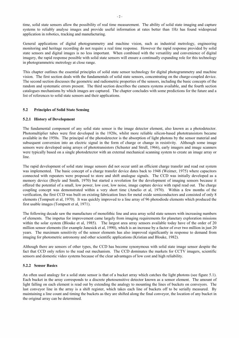
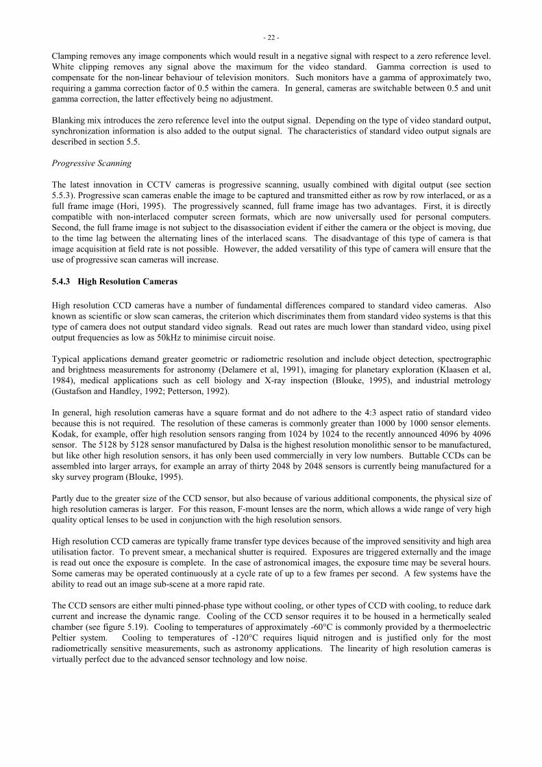
time, solid state sensors allow the possibility of real time measurement. The ability of solid state imaging and capture systems to reliably analyse images and provide useful information at rates better than 1Hz has found widespread application in robotics, tracking and manufacturing. General applications of digital photogrammetry and machine vision, such as industrial metrology, engineering monitoring and heritage recording do not require a real time response. However the rapid response provided by solid state sensors and digital images is no less important. When combined with the versatility and convenience of digital imagery, the rapid response possible with solid state sensors will ensure a continually expanding role for this technology in photogrammetric metrology at close range. This chapter outlines the essential principles of solid state sensor technology for digital photogrammetry and machine vision. The first section deals with the fundamentals of solid state sensors, concentrating on the charge-coupled device. The second section discusses the geometric and radiometric properties of the sensors, including the basic concepts of the random and systematic errors present. The third section describes the camera systems available, and the fourth section catalogues mechanisms by which images are captured. The chapter concludes with some predictions for the future and a list of references to solid state sensors and their applications. 5.2 Principles of Solid State Sensing 5.2.1 History of Development The fundamental component of any solid state sensor is the image detector element, also known as a photodetector. Photomultiplier tubes were first developed in the 1920s, whilst more reliable silicon-based phototransistors became available in the 1950s. The principal of the photodetector is the absorption of light photons by the sensor material and subsequent conversion into an electric signal in the form of charge or change in resistivity. Although some image sensors were developed using arrays of phototransistors (Schuster and Strull, 1966), early imagers and image scanners were typically based on a single photodetector with an external mechanical scanning system to create an image array or line. The rapid development of solid state image sensors did not occur until an efficient charge transfer and read out system was implemented. The basic concept of a charge transfer device dates back to 1948 (Weimer, 1975) where capacitors connected with repeaters were proposed to store and shift analogue signals. The CCD was initially developed as a memory device (Boyle and Smith, 1970) but started a revolution for the development of imaging sensors because it offered the potential of a small, low power, low cost, low noise, image capture device with rapid read out. The charge coupling concept was demonstrated within a very short time (Amelio et al, 1970). Within a few months of the verification, the first CCD was built on existing fabrication lines for metal oxide semiconductors and consisted of only 8 elements (Tompsett et al, 1970). It was quickly improved to a line array of 96 photodiode elements which produced the first usable images (Tompsett et al, 1971). The following decade saw the manufacture of monolithic line and area array solid state sensors with increasing numbers of elements. The impetus for improvement came largely from imaging requirements for planetary exploration missions within the solar system (Blouke et al, 1985). The largest area array sensors available today have of the order of 20 million sensor elements (for example Janesick et al, 1990), which is an increase by a factor of over two million in just 20 years. The maximum sensitivity of the sensor elements has also improved significantly in response to demand from imaging for photometric astronomy and other scientific applications (Kristian and Blouke, 1982). Although there are sensors of other types, the CCD has become synonymous with solid state image sensor despite the fact that CCD only refers to the read out mechanism. The CCD dominates the markets for CCTV imagers, scientific sensors and domestic video systems because of the clear advantages of low cost and high reliability. 5.2.2 Sensor Basics An often used analogy for a solid state sensor is that of a bucket array which catches the light photons (see figure 5.1). Each bucket in the array corresponds to a discrete photosensitive detector known as a sensor element. The amount of light falling on each element is read out by extending the analogy to mounting the lines of buckets on conveyors. The last conveyor line in the array is a shift register, which takes each line of buckets off to be serially measured. By maintaining a line count and timing the buckets as they are shifted along the final conveyor, the location of any bucket in the original array can be determined.
- 3 -
Figure 5.1 Bucket array analogy for a solid state imager (redrawn and adapted from Janesick and Blouke, 1987).
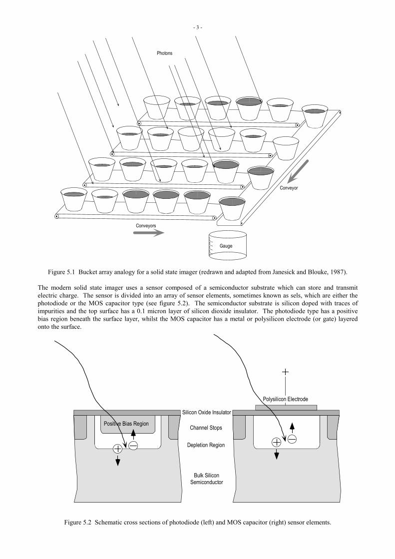
The modern solid state imager uses a sensor composed of a semiconductor substrate which can store and transmit electric charge. The sensor is divided into an array of sensor elements, sometimes known as sels, which are either the photodiode or the MOS capacitor type (see figure 5.2). The semiconductor substrate is silicon doped with traces of impurities and the top surface has a 0.1 micron layer of silicon dioxide insulator. The photodiode type has a positive bias region beneath the surface layer, whilst the MOS capacitor has a metal or polysilicon electrode (or gate) layered onto the surface.
Figure 5.2 Schematic cross sections of photodiode (left) and MOS capacitor (right) sensor elements.
Photons
Gauge
Conveyors
Conveyor
Silicon Oxide Insulator
Polysilicon Electrode
Bulk SiliconSemiconductor
Depletion Region
Positive Bias Region Channel Stops

- 4 -
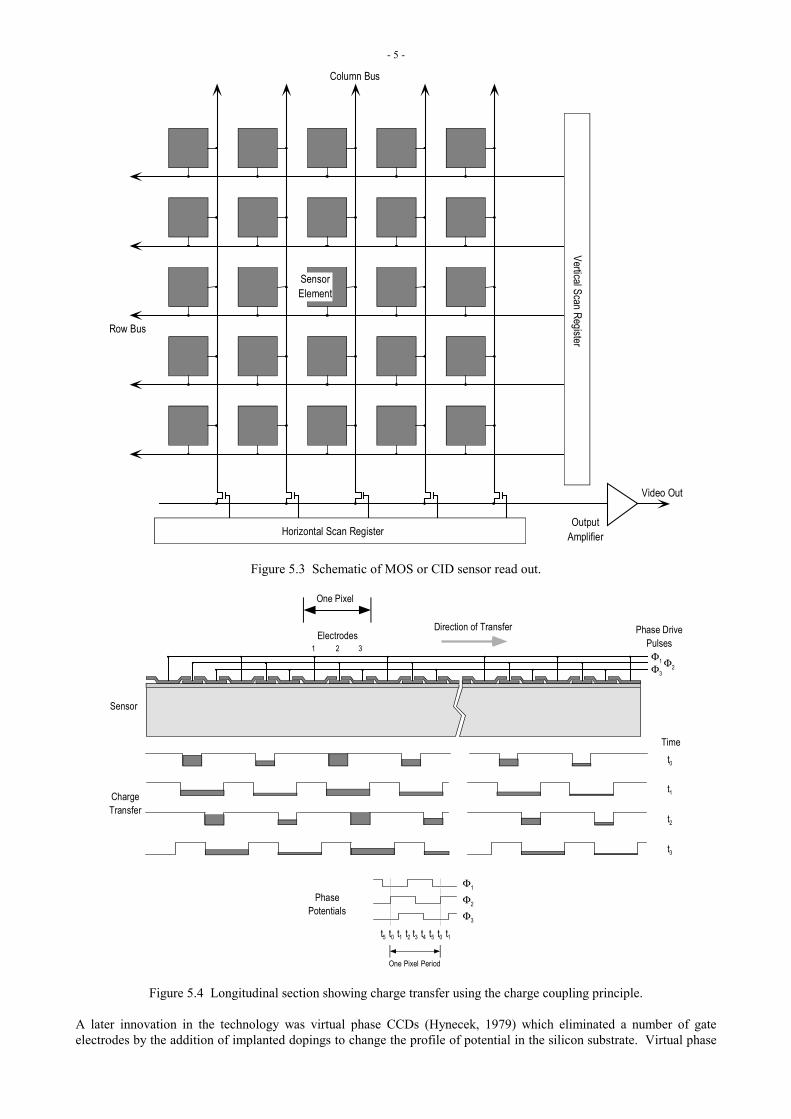
Light photon absorption below the surface of the sensor gives rise to electron-hole pairs at each sensor element. The electron is free to move within the silicon crystal lattice or re-combine with a hole, which is a temporary absence of an electron in the regular crystalline structure. The positive bias region or the positively charged electrode attracts the negative charges and the electrons are accumulated in the depletion region just below the sensor surface. Due to the presence of the electric field, the zone of accumulation is also known as a “potential well”, in which the electrons are “trapped”. Intrinsic absorption in the silicon is the fundamental effect for the visible and near infra-red regions of the spectrum. The energy required to liberate electrons from the silicon is such that detection of radiation is good in the spectral range of 400 to 1100 nanometres. Outside of this range, silicon is opaque to ultra-violet and transparent to infra-red, respectively. Sensors used for visible light band imaging often use an infra-red filter to limit the response outside the desired wavelength range. However the sensor elements always accumulate charge from thermal effects in the substrate material, leading to a background noise known as dark current. The name is a consequence of the fact that this noise is accumulated regardless of whether the sensor is exposed to or protected from incident light. Dark current generated at the surface is two to three orders of magnitude greater than the dark current generated in the substrate bulk. Extrinsic absorption at impurity sites is the detection mechanism for longer wavelengths in the electromagnetic spectrum. The additional spectral sensitivity of the sensor at longer wavelengths is dependent on the type of impurities introduced. The depth penetration of photons into the sensor is dependent on wavelength. Longer wavelength radiation penetrates more deeply, so impurities can be introduced throughout the sensor. There is essentially a linear relationship between the number of photons detected and the number of electron-hole pairs, and therefore the charge level, generated. The capacity of the potential wells is finite and varies depending on the type of sensor. If the well capacity is exceeded then the charge can overflow into neighbouring sensor elements, giving rise to a phenomenon commonly known as blooming. To prevent blooming and contain the charge during read out, rows of sensor elements are isolated within the transfer channel by electrodes, oxide steps or channel stops, with the latter being most common. The size of the channel stops reduces the proportion of the area of the light sensitive elements, relative to the sensor as a whole (see figure 5.2). 5.2.3 Sensor Read Out The charge at each sensor element must be transferred out of the sensor so that it can be measured. There are three schemes for charge read out which are in use for commercially available sensors. MOS capacitor and CID sensors use sense lines connected to read out registers and an amplifier (see figure 5.3). MOS capacitor sensors are also known as self-scanned photodiode arrays. The use of sense lines leads to fixed pattern noise due to spatial variations in the lines, and increased random noise because the sense line capacity is high compared to the sensor elements. However MOS and CID sensors are capable of random access to sensor elements, so particular regions of the sensor can be read out independently of the total image. The charge read out process in CID sensors can be non-destructive so that parts or all of the image can be repeatedly captured, whereas the read out of CCD and MOS capacitor sensors destroys the image. As previously noted, the mechanism used by CCD imagers is by far the most common type of sensor read out. As has been described, the charge is transferred from element to element like a bucket brigade. Charge coupling refers to the process by which pairs of electrodes are used to transfer the charge between adjacent potential wells. To continue the hydraulic analogy of the bucket brigade, the electrode voltages are manipulated in a sequence which passes the accumulated charge from one well to the next (see figure 5.4). At the end of the line of sensors the charge is transferred to output registers and scanned by an amplifier which has the same capacitance as a sensor element, thereby reducing noise. Surface and buried channel CCDs refer to the level in the sensor at which the charge is transferred. Buried channel CCDs require two different types of sensor substrate to lower the zone of charge accumulation. The buried channel type can transfer charge at higher speed with less noise, but has a lower charge handling capacity which reduces the dynamic range. The number of phases of the CCD refers to the number of electrodes and number of potential changes used in the transfer of charge between each sensor element. Two phase CCDs require additional complexity in the substrate to determine the direction of the charge transfer. Three phase CCDs are most common, whilst four phase CCDs have a greater charge handling capacity The operation of the phase gates requires some overlap, leading to a layering of electrodes and insulation, and therefore a sensor surface with a significant micro-topography.
- 5 -
Figure 5.3 Schematic of MOS or CID sensor read out.
Figure 5.4 Longitudinal section showing charge transfer using the charge coupling principle.
A later innovation in the technology was virtual phase CCDs (Hynecek, 1979) which eliminated a number of gate electrodes by the addition of implanted dopings to change the profile of potential in the silicon substrate. Virtual phase
SensorElement
Row Bus
Column Bus
Horizontal Scan Register
Vertical Scan Register
OutputAmplifier
Video Out
Phase DrivePulsesΦ1 Φ2Φ3
One Pixel
1 2 3Electrodes
Direction of Transfer
Time
t3
t2
t1
t0
Sensor
ChargeTransfer
Φ1
Φ2
Φ3
PhasePotentials
t0 t1 t2 t3 t4 t5 t0t5
One Pixel Period
t1

- 6 -
CCDs improve the charge capacity and lower noise, as well as reduce the surface topography. The open pinned-phase CCD (Janesick, 1989) is a combination of virtual phase and three phase which further reduces noise. The most recent innovation is multi pinned-phase CCDs which have additional doping to operate with an inverted potential between the surface and the substrate. This technique substantially reduces thermal noise in the form of dark current generated at the surface. A review of the different types of CCD architectures can be found in Janesick and Elliott (1992) whilst a discussion of the history and potential of CCD imagers can be found in Seitz et al (1995). 5.3 Geometric and Radiometric Properties of CCD Sensors 5.3.1 Sensor Layout and Surface Geometry The uniformity of the sensor elements and the flatness of the sensor surface are very important factors if CCD sensors are to be used for photogrammetry. The accuracy of fabrication of the sensor has direct impact on the application of the principle of collinearity. Geometry of Sensor Elements CCD sensors are fabricated by deposition of a series of layers on the silicon substrate. Each layer serves a particular purpose, such as insulation or gates. The geometry of the deposited layers is controlled by a photolithography process which is common to the manufacture of all integrated circuits based on silicon wafers. Photolithography uses masks which are prepared at a much larger size than the finished product and applied using optical or photographic reduction techniques. The unmasked area is sensitised to deposition using ultra-violet light or doping material, and the vaporised material which is introduced is then deposited only onto those areas. Alternatively, the surface is exposed to vapour etching and material is removed only from the unmasked areas. The limit of geometric accuracy and precision of CCD sensors can be deduced from the accuracy and precision of the lithographic process. The current generation of microprocessors are fabricated to 0.3 to 0.5 micrometre design rules, which require alignment accuracies of better than 0.1 micrometres. This alignment accuracy is supported by Pol et al (1987) who suggest the possibility of local systematic effects of 1/60th and an RMS error of 1/100th of the sensor element spacing on an eight millimetre square format. It could be expected that these 1/60th to 1/100th levels of fabrication error would also hold for larger format sensors due to the nature of the lithography process. Direct and indirect measurement of sensors has also indicated similar levels of accuracy and precision. Measurement of a CID array sensor using a travelling microscope indicated the mean sensor spacing to be within 0.2 micrometres of the 45 micrometre specification (Curry et al, 1986). An investigation of linear arrays using a knife edge technique showed that errors in the sensor spacing were less than 0.2 micrometres and the regularity of the spacing was “excellent” (Hantke et al, 1985). This corresponds to 1/70th of the spacing for the 13 micrometre element size. Sensors used for star tracking have indicated error limits of 1/100th of the element spacing based on the residuals of measurement from centroids (Stanton et al, 1987). This level of error is attributed to sensor non-uniformities, as the trackers have a very narrow field of view and are back-side illuminated, which removes the influence of surface micro-topography. Surface Flatness The flatness of the CCD sensor is an issue for both the overall shape of the silicon substrate and the micro-topography of the surface. Early CCD sensors were of low resolution and, more importantly, had small formats. Therefore, overall surface flatness was of little concern. With increases in sensor resolution have come increases in format size, so maximum angles of incidence near the edge of the format have risen to as great as 45 degrees. With some exceptions, very few CCD manufacturers specify the flatness of the sensor surface, largely because most sensors are prepared for broadcast or domestic markets which are not concerned with geometric quality. Thompson CSF specify an unflatness tolerance of 10 micrometres, corner to corner, for their 1024 by 1024 array sensor. With an element spacing of 19 micrometres, the diagonal of the format is therefore 27.5 millimetres and a 14 millimetre lens would produce angles of incidence approaching 45 degrees. Flatness errors of this order of magnitude are certainly significant and require correction for very precise applications of CCD sensors. Although the results of a study of unflatness of a Kodak 1524 by 1012 array sensor were inconclusive, the investigation did indicate that errors of the order of 10 micrometres were present (Fraser et al, 1995). The results did indicate clearly that unflatness effects are manifest as a degradation in the overall performance of the CCD sensor, but cannot readily be modelled and eliminated by photogrammetric self-calibration.
- 7 -
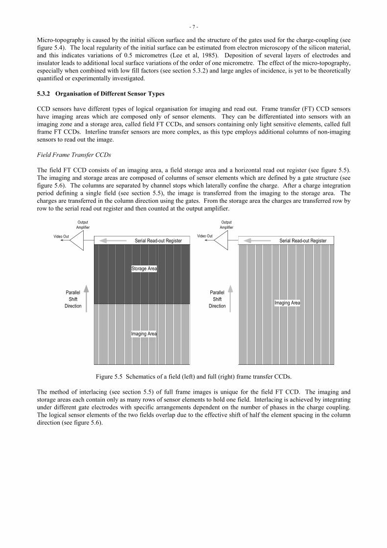
Micro-topography is caused by the initial silicon surface and the structure of the gates used for the charge-coupling (see figure 5.4). The local regularity of the initial surface can be estimated from electron microscopy of the silicon material, and this indicates variations of 0.5 micrometres (Lee et al, 1985). Deposition of several layers of electrodes and insulator leads to additional local surface variations of the order of one micrometre. The effect of the micro-topography, especially when combined with low fill factors (see section 5.3.2) and large angles of incidence, is yet to be theoretically quantified or experimentally investigated. 5.3.2 Organisation of Different Sensor Types CCD sensors have different types of logical organisation for imaging and read out. Frame transfer (FT) CCD sensors have imaging areas which are composed only of sensor elements. They can be differentiated into sensors with an imaging zone and a storage area, called field FT CCDs, and sensors containing only light sensitive elements, called full frame FT CCDs. Interline transfer sensors are more complex, as this type employs additional columns of non-imaging sensors to read out the image. Field Frame Transfer CCDs The field FT CCD consists of an imaging area, a field storage area and a horizontal read out register (see figure 5.5). The imaging and storage areas are composed of columns of sensor elements which are defined by a gate structure (see figure 5.6). The columns are separated by channel stops which laterally confine the charge. After a charge integration period defining a single field (see section 5.5), the image is transferred from the imaging to the storage area. The charges are transferred in the column direction using the gates. From the storage area the charges are transferred row by row to the serial read out register and then counted at the output amplifier.
Figure 5.5 Schematics of a field (left) and full (right) frame transfer CCDs.
The method of interlacing (see section 5.5) of full frame images is unique for the field FT CCD. The imaging and storage areas each contain only as many rows of sensor elements to hold one field. Interlacing is achieved by integrating under different gate electrodes with specific arrangements dependent on the number of phases in the charge coupling. The logical sensor elements of the two fields overlap due to the effective shift of half the element spacing in the column direction (see figure 5.6).
Video Out
OutputAmplifier
Serial Read-out Register
ParallelShift
Direction
Serial Read-out Register
OutputAmplifier
ParallelShift
Direction Imaging Area
Imaging Area
Storage Area
Video Out

- 8 -
Figure 5.6 Schematic of a sensor element layout for a four phase, field frame transfer CCD.
Full-frame Frame Transfer CCDs Full frame FT CCD sensors have the simplest structure of any area array CCD. The sensor comprises only an imaging area and a serial read out register (see figure 5.5). The charges are read out directly after the integration period for each field or the full frame. The charge transfer process for both types of FT array requires that steps must be taken to prevent significant smearing of the image. Smear is caused by the fact that the sensor elements are exposed to light during the read out process, and the same sensor elements are used to expose the image and transfer the charge. A straightforward technique for eliminating smear is a mechanical shutter to cover the sensor during charge read out. Other techniques for minimising smear are described in the next section. The simple structure of FT CCDs makes it possible to fabricate very small sensor elements. For example, the Kodak KAF series of CCDs have 6.8 micrometre sensor elements. The sensitive area of the CCD surface is only interrupted by channel stops and therefore has an area utilisation factor approaching 100%. This may be reduced somewhat if anti-
Odd FieldSensor Element
Half SensorElement Spacing
ChannelStop
Φ4
Φ3
Φ2
Φ1
Electrodes
ShiftDirection
Even FieldSensor Element
- 9 -
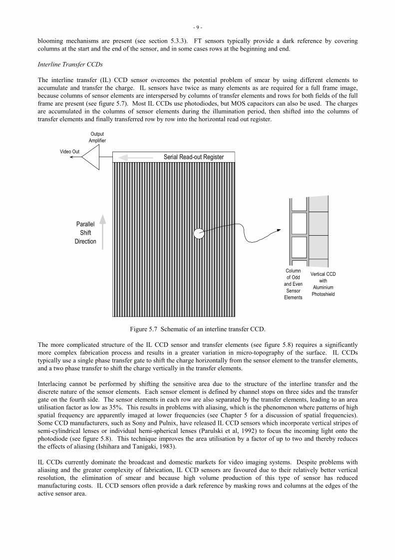
blooming mechanisms are present (see section 5.3.3). FT sensors typically provide a dark reference by covering columns at the start and the end of the sensor, and in some cases rows at the beginning and end. Interline Transfer CCDs The interline transfer (IL) CCD sensor overcomes the potential problem of smear by using different elements to accumulate and transfer the charge. IL sensors have twice as many elements as are required for a full frame image, because columns of sensor elements are interspersed by columns of transfer elements and rows for both fields of the full frame are present (see figure 5.7). Most IL CCDs use photodiodes, but MOS capacitors can also be used. The charges are accumulated in the columns of sensor elements during the illumination period, then shifted into the columns of transfer elements and finally transferred row by row into the horizontal read out register.
Figure 5.7 Schematic of an interline transfer CCD.
The more complicated structure of the IL CCD sensor and transfer elements (see figure 5.8) requires a significantly more complex fabrication process and results in a greater variation in micro-topography of the surface. IL CCDs typically use a single phase transfer gate to shift the charge horizontally from the sensor element to the transfer elements, and a two phase transfer to shift the charge vertically in the transfer elements. Interlacing cannot be performed by shifting the sensitive area due to the structure of the interline transfer and the discrete nature of the sensor elements. Each sensor element is defined by channel stops on three sides and the transfer gate on the fourth side. The sensor elements in each row are also separated by the transfer elements, leading to an area utilisation factor as low as 35%. This results in problems with aliasing, which is the phenomenon where patterns of high spatial frequency are apparently imaged at lower frequencies (see Chapter 5 for a discussion of spatial frequencies). Some CCD manufacturers, such as Sony and Pulnix, have released IL CCD sensors which incorporate vertical stripes of semi-cylindrical lenses or individual hemi-spherical lenses (Parulski et al, 1992) to focus the incoming light onto the photodiode (see figure 5.8). This technique improves the area utilisation by a factor of up to two and thereby reduces the effects of aliasing (Ishihara and Tanigaki, 1983). IL CCDs currently dominate the broadcast and domestic markets for video imaging systems. Despite problems with aliasing and the greater complexity of fabrication, IL CCD sensors are favoured due to their relatively better vertical resolution, the elimination of smear and because high volume production of this type of sensor has reduced manufacturing costs. IL CCD sensors often provide a dark reference by masking rows and columns at the edges of the active sensor area.
Serial Read-out Register
OutputAmplifier
ParallelShift
Direction
Video Out
Vertical CCDwith
AluminiumPhotoshield
Columnof Odd
and EvenSensor
Elements

- 10 -
Figure 5.8 Schematic cross section of an interline transfer sensor with semi-cylindrical lenses.
Colour Solid state sensors are inherently achromatic, in the sense that they image across a wide range of the visible and near-visible spectrum (see section 5.3.5). The images recorded, like conventional panchromatic film, are an amalgamation across the spectral sensitivity range of the sensor. The lack of specific colour sensitivity results in so-called monochrome images, in which only luminance, or image brightness, is represented as a grey scale of intensity. Colour can be introduced by one of two methods. The first possibility is for three images to be exposed of the same scene, one in each of three standard spectral bands such as red, green and blue (RGB) or cyan, magenta and yellow (CMY). The three images can be acquired by a colour filter wheel, which is rotated in front of the sensor, or by using three sensors with permanent filters which image the same scene through beam splitters. Clearly, the camera and object must be stable for the former, and image registration must be accurate for the latter, to obtain a representative colour image. Cameras with three CCDs are widely used in the broadcast television industry. The second method employs band sensitised striping on the sensor elements. Typically, colour is acquired row by row, and each horizontal line of elements is doped or coated to be sensitive to a narrow spectral band. Many manufacturers use the row scheme of GRGBGRGB... or alternating rows of GRGR... and BGBG... as the human eye is most sensitive to the yellow-green band in the visible spectrum. Because the human eye is more sensitive to strong variations in light intensity than similar variations in colour, some CCD sensors have 75% green elements and 25% red and blue elements (Parulski et al, 1992). Each row of elements is then given a red, green and blue value according to a computation scheme based on the adjacent rows or a three by three matrix around individual elements. As the computation process is effectively an averaging or re-sampling of sensor element intensities, image artefacts can sometimes be produced by striping or edges in the object. The advantage of this scheme is that only a single CCD and single exposure is necessary, so it is widely used. Monochrome images should not be derived from such sensors by averaging the three bands, as this leads to a double averaging of the image which acts effectively as a smoothing filter and reduces the discrimination in the image (Shortis et al, 1995).
5.3.3 Spurious Signals Spurious signals from CCDs are systematic or transient effects which are caused by faults in the fabrication of CCD sensors or deficiencies in the technology of CCDs. The most important effects are dark current, blooming, smear, traps and blemishes. All of these effects result in degradation of the image quality and can be detected by inspection of images or minimised by radiometric calibration of the sensor.
Semi-cylindricalLens
SensorElement
Aluminium Photoshieldand Vertical CCD Electrode
Channel StopTransfer Gate

- 11 -
Dark Current The thermal generation of minority carriers, electrons in the case of silicon, produced in any semiconductor is known as dark current. In CCD sensors, dark current cannot be distinguished from charge generated by incident light. The dark current is produced continuously at a rate proportional to the absolute temperature of the sensor material. Sensor elements slowly fill with charge even without illumination, reaching full capacity over a period known as the storage time. Dark current is produced at different rates depending on the depth within the sensor. The surface component is generated at the silicon to silicon dioxide interface and is normally the dominant source at room temperature. The diffusion component generated in the bulk of the substrate region is typically a few orders of magnitude less, although the rate of variation varies depending on the quality of the silicon (Janesick and Elliott, 1992). The dark current for individual images is generated during both the illumination and read out phases. IL CCDs have longer illumination times and therefore accumulate more dark current and noise. As the various sensor elements require different times to be read out, the dark current level will vary leading to a slope of dark current noise across the image (Hopkinson et al, 1987). The slope is generally linear, although the generation will not be uniform over any particular sensor due to blemishes and other effects, resulting in a fixed pattern noise. Fixed pattern noise is a limit on the minimum detectable signal. It is also dependent on temperature and the pattern can change significantly (Purll, 1985), requiring any calibration to be conducted at the operating temperature of the sensor. There are two common techniques used for the reduction of dark current. Dark current is strongly correlated with operating temperature, and a reduction of 5-10°C decreases the generation of noise by a factor of two. Many “scientific” CCDs incorporate Peltier cooling systems to reduce the operating temperature to around -50°C in order to improve the dynamic range and therefore the radiometric sensitivity of the sensor. As described in section 5.2.3, multi pinned-phase CCDs have very low dark current rates at room temperature, and are preferred because the expensive and cumbersome cooling systems can be discarded. Broadcast and domestic video systems do not yet warrant multi pinned-phase CCDs because the illumination times are very short. However, this type of CCD sensor is useful for astronomic telescope imagers and still video industrial inspection systems, as illumination times can be considerably longer (see section 5.4). Blooming When too much light falls onto a sensor element or group of sensor elements, the charge capacity of the wells can be exceeded. The excess charge then spills over into neighbouring elements, just as if the buckets in the bucket array analogy are over-filled. The effect is known as blooming and is most commonly associated with intense light sources, such as the response of retro-reflective targets to a light flash. Blooming can be readily detected by the excess spread of such light sources in the image, or image trails left by excess charge during read out (see figure 5.9).
Figure 5.9 Blooming on a frame transfer sensor caused by intense retro-reflective target illumination.

- 12 -
Although blooming cannot be totally eliminated from CCD sensors, the inclusion of so called anti-blooming drains has dramatically reduced the problem in the current generation of CCDs, as compared to the first CCD sensors. Vertical anti-blooming structures (for example Collet et al, 1985) use a special deep diffusion to produce a potential profile which draws extra charge into the substrate. Horizontal anti-blooming methods (for example Kosonocky et al, 1974) use additional gate electrodes and channel stops to drain off excess charge above a set threshold potential. Horizontal anti-blooming drains are placed adjacent to the transfer gates in IL CCDs and parallel to the channel stops in FT CCDs, reducing the area utilisation factor. As it is easier to prevent blooming across columns with these drains, blooming usually occurs within columns first. Whereas initial attempts at anti-blooming could control illumination levels only up to 100 times the saturation exposure, the limit rose steadily to levels of over 2000 times saturation for consumer products in the 1980s (Furusawa et al, 1986). The latest generation of consumer products have blooming control which can compensate for signals which are 10,000 times the saturation level of the sensor. Smear Smear describes the phenomenon that an intense light source influences the brightness in the column direction (see figure 5.10). The apparent effect of smear in the acquired image is very similar for all sensor types, but the physical source of smearing is different. Smear is usually defined as the ratio between the change in image brightness above or below a bright area covering 10% of the sensor extent in the column direction.
Figure 5.10 Image trails of intense light sources caused by smearing in a frame transfer CCD sensor (from Shortis and Snow, 1995).
In the absence of shuttering, smear in FT CCDs originates from the accumulation of charge during the transfer from the imaging to the storage zones. For a given area of brightness, the level of smear is proportional to the ratio between the illumination and transfer periods, which is typically 40 to 1. Hence for a 10% extent on the sensor, the smear will be 0.25% for a saturated image, which would normally not be evident. However, if the sensor is over-saturated by a large factor, the smear is visible as image trails. Smear can be reduced dramatically in FT CCDs by reducing the transfer time (Furusawa et al, 1986). In a similar mechanism to the FT CCD, the smear for IL CCD sensors is a result of light penetration during the charge transfer period. However in this case the charge generation giving rise to smear is indirect. Light at the edges of the sensor element can reach the transfer element, light can be piped into the transfer element by the surface structures and long wavelength photons can penetrate the shielding of the transfer element. Smear for a 1024 by 1024 area array IL CCD sensor has been determined to be 0.1%, primarily due to light piping (Stevens et al, 1990). Again, over-saturation of the image by intense light sources will result in image trails such as those shown in figure 5.10. Traps Traps are defect sites caused by a local degradation in the charge transfer efficiency. Traps capture charges from charge packets being transferred and release the trapped charge slowly once there is an equilibrium of charge in the trap. Traps originate from design flaws, material deficiencies and defects induced from the fabrication process.

- 13 -
The frequency of trap defects can be reduced by improving the quality of materials and the fabrication process. An alternative method is to always keep the traps filled with charge. A bias level of charge, or so called fat zero, is introduced prior to charge accumulation and then subtracted during read out. This technique has the disadvantage of reducing the dynamic range of the sensor. Traps can be detected as short, dark lines which tend to lengthen with lowering intensity of uniformly bright (flat field) images (Yang et al, 1989). For room temperature CCD sensors, traps are less prevalent as they are swamped by dark current. Blemishes Blemishes on acquired images from CCD sensors are caused by material deficiencies, such as crystallographic defects in the silicon, or defects induced by the fabrication process. Such defects introduce dark current or other effects which exceed the specification for the CCD sensor and are manifest as a spurious signal in the image. Blemishes are characterised by type as single point, area or linear, which effect a single sensor element, a group of adjacent elements or a column respectively. Single point and area blemishes are most often caused by small sources of dark current or shorts between gates or between gates and the substrate. Sensor elements with exceptionally high dark current are known as dark current spikes and produce white spots or areas. Area blemishes can take different shapes, such as “swirl patterns”, “white clouds” or “swiss cheese” (Murphy, 1979). Column defects in IL CCD sensors are usually due to fabrication deficiencies in channel stops. Sensors with row defects are generally culled by the manufacturer. A blemish compensation circuit is included in some CCD cameras to remove defects in images output by the sensor. The addresses of the defects are stored in read only memory as a table of locations. The sensor elements ahead of each blemish are read twice by the scanning circuits and then output as sequential elements to disguise the defect. Some manufacturers classify their sensors according to the number and location of blemishes. For example, Class 1 Dalsa 2048 by 2048 sensors are virtually blemish free, having less than 100 point defects, 5 area defects and no column defects in the central zone of the sensor. In contrast, Class 3 sensors have up to 500 point blemishes, 50 area blemishes and 10 column defects. The central zone is defined as the central area containing 75% of the array extent, and area defects are defined as cluster of no more than 20 sensor elements. Other manufacturers have similar specifications, often with more stringent limits for sensors produced for scientific applications. In general, the limits on blemishes are proportional to the total number of elements in the sensor. For example, a Class 3 Dalsa 5120 by 5120 sensor has a 2500 point defect limit.
Figure 5.11 Types of image defects typically present for lesser class CCD sensors.
- 14 -
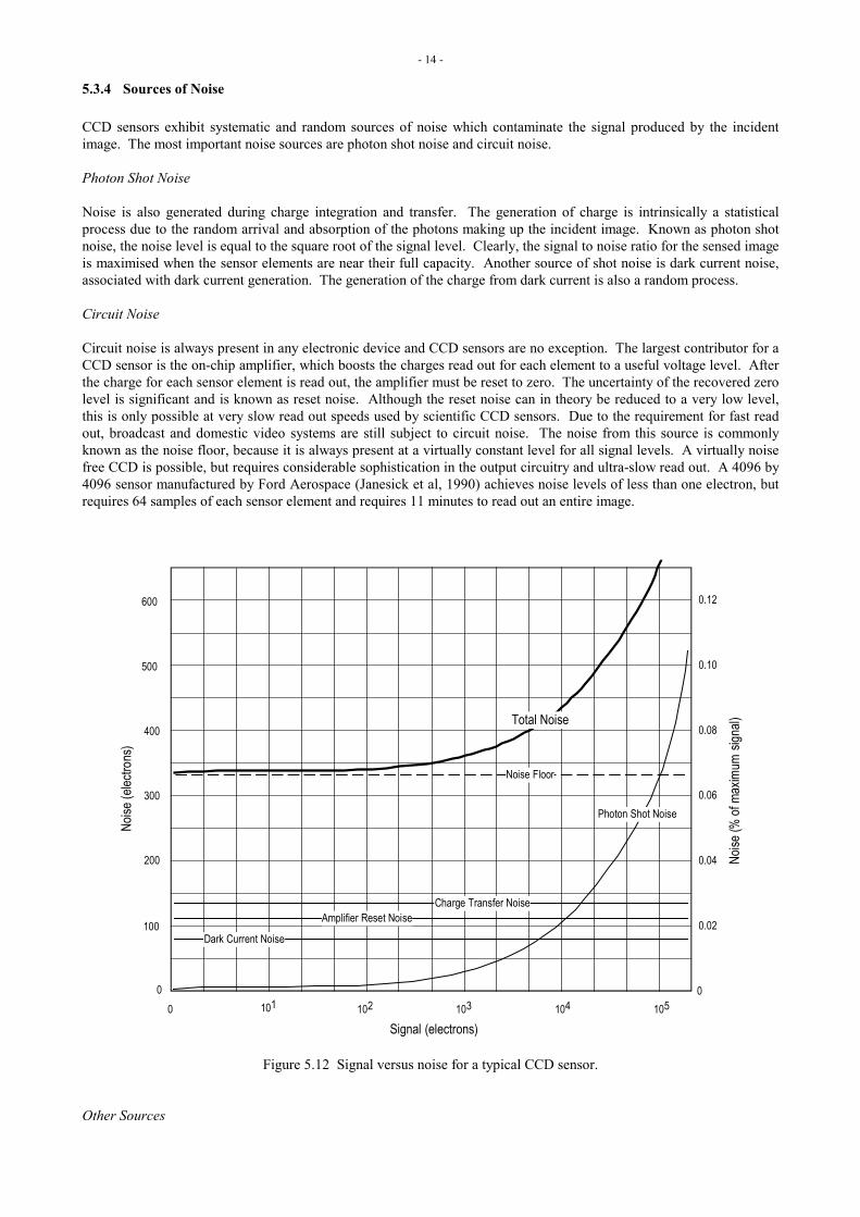
5.3.4 Sources of Noise CCD sensors exhibit systematic and random sources of noise which contaminate the signal produced by the incident image. The most important noise sources are photon shot noise and circuit noise. Photon Shot Noise Noise is also generated during charge integration and transfer. The generation of charge is intrinsically a statistical process due to the random arrival and absorption of the photons making up the incident image. Known as photon shot noise, the noise level is equal to the square root of the signal level. Clearly, the signal to noise ratio for the sensed image is maximised when the sensor elements are near their full capacity. Another source of shot noise is dark current noise, associated with dark current generation. The generation of the charge from dark current is also a random process. Circuit Noise Circuit noise is always present in any electronic device and CCD sensors are no exception. The largest contributor for a CCD sensor is the on-chip amplifier, which boosts the charges read out for each element to a useful voltage level. After the charge for each sensor element is read out, the amplifier must be reset to zero. The uncertainty of the recovered zero level is significant and is known as reset noise. Although the reset noise can in theory be reduced to a very low level, this is only possible at very slow read out speeds used by scientific CCD sensors. Due to the requirement for fast read out, broadcast and domestic video systems are still subject to circuit noise. The noise from this source is commonly known as the noise floor, because it is always present at a virtually constant level for all signal levels. A virtually noise free CCD is possible, but requires considerable sophistication in the output circuitry and ultra-slow read out. A 4096 by 4096 sensor manufactured by Ford Aerospace (Janesick et al, 1990) achieves noise levels of less than one electron, but requires 64 samples of each sensor element and requires 11 minutes to read out an entire image.
Figure 5.12 Signal versus noise for a typical CCD sensor.
Other Sources
0
200
300
400
500
600
105104103102
Signal (electrons)
Noise
(elec
trons
)
0 101
Photon Shot Noise
Dark Current Noise
Amplifier Reset Noise
Total Noise
Noise Floor
Charge Transfer Noise
Noise
(% of
max
imum
sign
al)
0
0.04
0.06
0.08
0.10
0.12
0.02100

- 15 -
Other intrinsic noise sources are charge transfer noise, fat zero noise and the previously mentioned dark current noise. Charge transfer noise is present due to random fluctuations in the transfer efficiencies of the elements. It is proportional to the square root of the number of transfers and the signal level. As various elements require more transfers than others to be read out, charge transfer noise also contributes to a noise slope across the image and therefore to the fixed pattern noise produced by the sensor. Using the estimates of various noise sources, both constant and signal dependent, a total noise budget can be estimated for a standard CCD sensor at room temperature. From the graph depicted in figure 5.12, it is clear that low intensity images can be indistinguishable from noise, whilst high intensity images with a large signal strength have an excellent signal to noise ratio.
5.3.5 Spectral Response and Radiometry Spectral Response Solid state imagers are commonly front side illuminated (see figure 5.13), which requires the incident light to pass through several layers of structures, such as gates and insulation, before being absorbed by the silicon. Short wavelength light will be absorbed by the polysilicon and silicon dioxide in these structures, reducing the sensitivity in the ultra-violet and blue regions of the spectrum because these wavelengths of light have minimal penetration into the silicon. Despite this limitation, CCD sensors have a much wider spectral response than the human eye or photographic emulsions (see figure 5.14).
Figure 5.13 Schematics of front side (left) and thinned, back side (right) illuminated CCD sensors.
Transparent gate materials, such as tin and indium oxide, can be used to improve the response for short wavelengths. Alternatively, gaps can be left between the gates to allow the ultra-violet and blue radiation to penetrate the silicon. This is the case for open pinned-phase CCDs, which have areas of ultra-thin silicon dioxide coating. The most successful method of extending the spectral sensitivity of CCD sensors is back side thinning and illumination. This technique requires the sensor to be precisely thinned down to a thickness of around eight micrometres, compared to the normal thickness of approximately 200 micrometres (Janesick et al, 1987). The incident light does not have to pass through the front side surface layers, realising a significant improvement in sensitivity. Back side illumination is commonly used for astronomic imaging applications, whereas extended sensitivity and spectral ranges, as well as the potential fragility of the thinned sensor, are not appropriate for other applications.

- 16 -
Figure 5.14 Spectral response for CCD sensors, photography and the human eye.
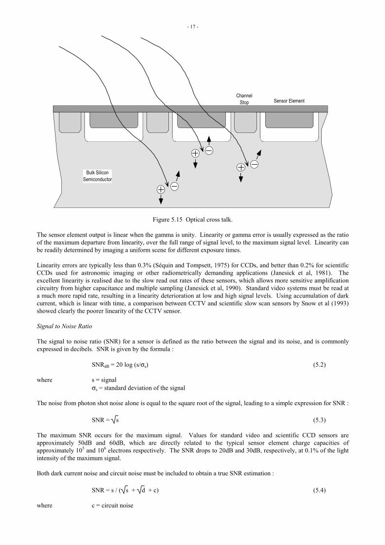
Infra-red filters are typically used to minimise the sensitivity of standard video sensors at wavelengths above 700 nanometres. As can be seen from figure 5.14, this limits the spectral range of the CCD sensor in the long wavelength band to approximately that of the human eye or a panchromatic photographic emulsion. The filter has the second effect of limiting optical cross talk. Longer wavelengths penetrate more deeply into the silicon of the sensor, increasing the possibility of light falling on one sensor element and generating charge in a neighbouring element. Whilst photons of blue light penetrate only 1 micrometre into the silicon, photons in the infra-red will reach virtually any depth. The charge generated by deeply penetrating photons will migrate randomly to the depletion regions leading ultimately to a blurring of the image (see figure 5.15). Wide angle lenses and large format sensors exacerbate this problem due to the large angles of incidence of light falling onto the sensor. Linearity The charge generation from incident illumination is inherently a linear process for solid state sensors, and ideally there should be a linear relationship between the light intensity and the signal level. However, the signal must be amplified and transmitted by electronic circuitry, which often does not have commensurate linearity. The output signal from a sensor element can be expressed as : s = k qγ + d (5.1) where s = output signal level k = constant of proportionality q = generated charge γ = gamma d = dark current signal
0.0
0.1
0.2
0.3
0.4
0.5
0.6
1000900800700600500400300
Wavelength (nanometres)
Relat
ive E
ff icien
cy
Thinned, Back Side Illuminated CCD
Front Side Illuminated CCD
Front Side Illuminated CCD with IR Filter
Panchromatic FilmHuman Eye
Violet RedGreen Yellow Infra Red
- 17 -
Figure 5.15 Optical cross talk.
The sensor element output is linear when the gamma is unity. Linearity or gamma error is usually expressed as the ratio of the maximum departure from linearity, over the full range of signal level, to the maximum signal level. Linearity can be readily determined by imaging a uniform scene for different exposure times. Linearity errors are typically less than 0.3% (Séquin and Tompsett, 1975) for CCDs, and better than 0.2% for scientific CCDs used for astronomic imaging or other radiometrically demanding applications (Janesick et al, 1981). The excellent linearity is realised due to the slow read out rates of these sensors, which allows more sensitive amplification circuitry from higher capacitance and multiple sampling (Janesick et al, 1990). Standard video systems must be read at a much more rapid rate, resulting in a linearity deterioration at low and high signal levels. Using accumulation of dark current, which is linear with time, a comparison between CCTV and scientific slow scan sensors by Snow et al (1993) showed clearly the poorer linearity of the CCTV sensor. Signal to Noise Ratio The signal to noise ratio (SNR) for a sensor is defined as the ratio between the signal and its noise, and is commonly expressed in decibels. SNR is given by the formula : SNRdB = 20 log (s/σs) (5.2) where s = signal σs = standard deviation of the signal The noise from photon shot noise alone is equal to the square root of the signal, leading to a simple expression for SNR : SNR = s (5.3) The maximum SNR occurs for the maximum signal. Values for standard video and scientific CCD sensors are approximately 50dB and 60dB, which are directly related to the typical sensor element charge capacities of approximately 105 and 106 electrons respectively. The SNR drops to 20dB and 30dB, respectively, at 0.1% of the light intensity of the maximum signal. Both dark current noise and circuit noise must be included to obtain a true SNR estimation : SNR = s / ( s + d + c) (5.4) where c = circuit noise
Sensor ElementChannel
Stop
Bulk SiliconSemiconductor

- 18 -
Hence the actual SNRs of the sensors will be degraded slightly compared to a sensor limited only by shot noise. The difference for scientific sensors is negligible, as shot noise predominates at all but the lowest signal levels due to their superior circuit design and dark current characteristics. Dynamic Range The dynamic range of an imager is defined as the ratio between the peak signal level and system noise level, or alternatively the ratio between the maximum sensor element charge capacity and the noise floor in electrons. Typical dynamic ranges for CCTV and scientific CCD sensors are 104 to 105, or 60dB to 100dB. These dynamic ranges assume circuit noise, primarily from the on-chip amplifier, of 10 and 100 electrons, although the latter figure may be significantly higher for some standard video CCD sensors. SNR and dynamic range can be increased by increasing the maximum charge capacity of the sensor elements. The charge capacity of the silicon is essentially proportional to the sensitive area of each element, given the same type of CCD technology. Capacity is therefore greater for sensors with larger sensor elements and larger area utilisation factors. In general, frame transfer type CCD sensors with large sensor elements will have the largest charge capacity, and therefore the greatest radiometric sensitivity. Non-Uniformity and Radiometric Calibration Photo-response non-uniformity (PRNU) is the term given to signal variations from element to element in a CCD sensor, given the same level and wavelength of incident illumination. PRNU is caused by a number of factors, such as variations in the area and spacing of the elements, fixed pattern noise from variations in the silicon substrate, as well as traps and blemishes. PRNU with low spatial frequency is known as shading and is caused by variations in read-out timing or register capacitance. PRNU is more dependent on the wavelength of the incident light than the light intensity and the temperature of the sensor (Purll, 1985). Hence the infra-red filter used on standard video CCD sensors also reduces PRNU. Non-uniformity can be corrected using a dark image, a flat field image and the image of interest. A dark image is an exposure with no incident light. In this context, a flat field is an exposure of a perfectly uniform source of light intensity, preferably set to give near full capacity charge for the sensor elements. This can be obtained from a specialised device known as an integrating sphere, which is a feature of some commercial scanning systems based on CCD sensors. A more accessible but lower quality alternative is any reasonably uniform light source, such as a clear blue or night sky, combined with removal of the lens and averaging of randomly displaced images. The radiometrically correct intensity for each sensor element is estimated by the formula : Ic = (Ir - Id) / (If - Id) (5.5) where Ic = corrected intensity for the element Ir = recorded intensity for the element Id = dark image intensity for the element If = flat field intensity for the element The formula is based on the assumption of linearity of response of the CCD sensor elements, and the corrected intensity must be re-scaled to a suitable range for the application. This process is computationally intensive for high resolution images and should only be applied where the integrity of the radiometry warrants the correction process. In the majority of close range and machine vision applications, the geometry of the sensor is of paramount importance to maintain metric accuracy and the radiometry is often a secondary issue.
- 19 -
5.4 CCD Camera Systems
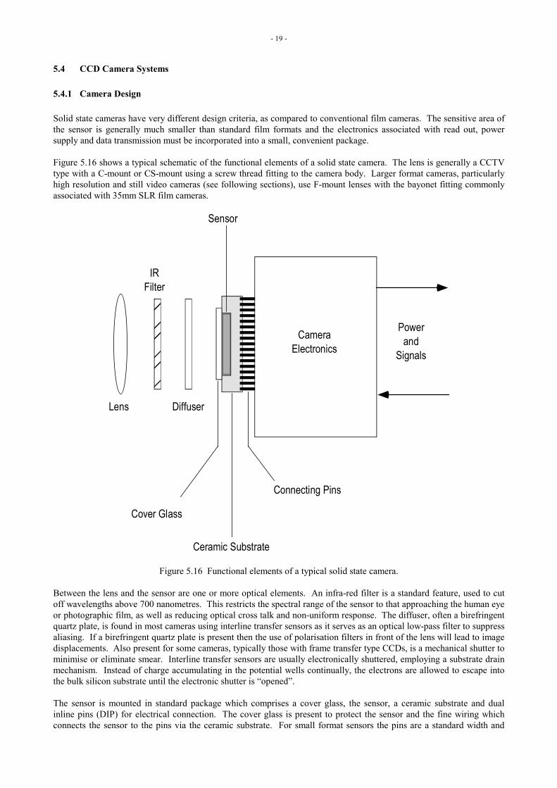
5.4.1 Camera Design Solid state cameras have very different design criteria, as compared to conventional film cameras. The sensitive area of the sensor is generally much smaller than standard film formats and the electronics associated with read out, power supply and data transmission must be incorporated into a small, convenient package. Figure 5.16 shows a typical schematic of the functional elements of a solid state camera. The lens is generally a CCTV type with a C-mount or CS-mount using a screw thread fitting to the camera body. Larger format cameras, particularly high resolution and still video cameras (see following sections), use F-mount lenses with the bayonet fitting commonly associated with 35mm SLR film cameras.
Figure 5.16 Functional elements of a typical solid state camera.
Between the lens and the sensor are one or more optical elements. An infra-red filter is a standard feature, used to cut off wavelengths above 700 nanometres. This restricts the spectral range of the sensor to that approaching the human eye or photographic film, as well as reducing optical cross talk and non-uniform response. The diffuser, often a birefringent quartz plate, is found in most cameras using interline transfer sensors as it serves as an optical low-pass filter to suppress aliasing. If a birefringent quartz plate is present then the use of polarisation filters in front of the lens will lead to image displacements. Also present for some cameras, typically those with frame transfer type CCDs, is a mechanical shutter to minimise or eliminate smear. Interline transfer sensors are usually electronically shuttered, employing a substrate drain mechanism. Instead of charge accumulating in the potential wells continually, the electrons are allowed to escape into the bulk silicon substrate until the electronic shutter is “opened”. The sensor is mounted in standard package which comprises a cover glass, the sensor, a ceramic substrate and dual inline pins (DIP) for electrical connection. The cover glass is present to protect the sensor and the fine wiring which connects the sensor to the pins via the ceramic substrate. For small format sensors the pins are a standard width and
Powerand
Signals
CameraElectronics
Connecting Pins
Ceramic Substrate
Cover Glass
Sensor
Lens
IRFilter
Diffuser

- 20 -
spacing to be accepted into DIP receptacles used on printed circuit boards. Larger sensors tend to have unique mountings and pin connections. The infra-red filter, diffuser and glass plate are typically not accounted for by the lens design and will reduce the optical performance of the system as a whole. In some cameras the infra-red filter is incorporated into the cover glass. In more recent cameras the diffuser has been replaced by semi-cylindrical lens striping on the sensor. Both of these innovations reduce the number or influence of refractive surfaces between the lens and the sensor. The mounting of the sensor and lens is often in question for solid state cameras, again because solid state sensors are designed for broadcast and domestic markets which are not concerned with geometric stability. Lens mounts may be loose or have poor alignment with respect to the sensor (Burner, 1995). The sensor itself may not be rigidly attached to the camera body (Gruen et al, 1995). In each of these cases remedial action can be taken to stabilise the components to ensure that a consistent camera calibration model can be determined and applied through either system calibration or self-calibration. Perhaps the most well known systematic effects present in cameras based on solid state sensors are those caused by warm up. As the sensor and the camera as a whole progress toward temperature equilibrium after power up, the output image will drift due to thermal expansion and drift in the electronics. This effect has been repeatedly confirmed for solid state cameras (Dähler, 1987; Beyer, 1992; Robson et al, 1993). Shifts of the order of tenths of a picture element (or pixel) are typical and it is generally accepted that CCD cameras require one to two hours to reach thermal equilibrium.
5.4.2 Standard Video Formats The most common type of solid state camera is based around a broadcast television format, uses an interline transfer type of CCD sensor, outputs a standard video signal (see section 5.5), and is often simply called a CCTV or video camera. This type of camera is used for applications such as television broadcasting, domestic video camcorders, security systems for surveillance, machine vision, real time photogrammetry and industrial metrology. The range of applications is best represented by recent conferences of Commission V of the International Society for Photogrammetry and Remote Sensing (Gruen and Baltsavias, 1990; Fritz and Lucas, 1992; Fryer and Shortis, 1994) and the Videometrics series of conferences (El-Hakim, 1993, 1994, 1995). Two examples of standard video format cameras are shown in figure 5.17.
Figure 5.17 Examples of standard video, scientific high resolution and still video cameras.
Broadcast formats, adopting the classic 4:3 ratio of width to height, originated from the earliest video tube cameras. Although the first area array solid state sensors were generally square in format, manufacturers have widely adopted broadcast formats as standard format sizes for CCD sensors. Early CCD cameras were used in CCTV systems and only in the last several years have solid state sensors been adopted for use by electronic news gathering cameras and broadcast systems. The range of CCD camera systems, in terms of features, quality, number of manufacturers and cost, is enormous. Broadcast formats are specified by the diagonal size (in inches) of the video camera tube. The horizontal and vertical sides are required to be in the specified 4:3 ratio. The first video standard CCD sensors were equivalent to a 2/3” tube, corresponding to a solid state sensor format of 5.8 by 6.6 millimetres. Due to improvements in manufacturing technology, format sizes have decreased (Seitz et al, 1995) and the current generation of CCD sensors are available in 1/2” and 1/3” formats, which correspond to 6.4 by 4.8 and 4.9 by 3.7 millimetres respectively. The resolution of the CCD sensors in terms of elements varies depending on the video standard, however typical resolutions are of the order of 700 horizontal pixels by 500 vertical pixels. Hence the spacing of the sensor elements varies from slightly more than 10 micrometres for the 2/3” format, down to approximately 5 micrometres for the 1/3” format. Fabrication of sensor elements smaller than 5 micrometres is unlikely due to the decrease in full well capacity and consequent loss of dynamic range. High Definition Television (HDTV) has been under development and standardisation for several years. Only during the last few years have CCD cameras been specifically developed for HDTV, adding a new 1” format to the list of “standard” video formats. For example Sony has released a 1920 by 1024 pixel sensor which outputs a HDTV video signal. The CCD sensor is 14 by 8 mm and has an aspect ratio of 16:9. This camera has been tested for photogrammetric use, and produced encouraging results (Peipe, 1995b.) Camera Electronics

- 21 -
A standard video camera incorporates onboard electronics to carry out a number of functions. For example, the camera must perform appropriate signal processing to minimise noise and maintain a constant reference voltage for the output signal. The synchronization and timing of input and output signals is critical for standard video cameras which output an analogue signal at high frequencies. The effective pixel output rate is typically greater than 10MHz.
Figure 5.18 Functional elements of a typical standard video camera.
Figure 5.18 shows a block diagram of a typical standard video camera. The camera requires a power unit to convert from external AC to internal DC supply if needed, and convert to the various DC voltages required by the electronic components. The external sync(hronization) detection performs two tasks. The first is to detect an external synchronization signal and set the camera to use this or the internal clock. The second is to convert the external synchronization signals into internal signals. The synchronization source is used to derive a master timing generator which drives the phases of the CCD sensor and controls the timing of the video output and synchronization signals. The output video signal is pre-processed to reduce noise. This can be a simple sample-and-hold or an advanced scheme such as multiple sampling. The automatic gain control (AGC) is a function to adjust the average image brightness. AGC attempts to adjust the average intensity of the image to a consistent level. It has the desirable effect of compensating for the ambient lighting, but the undesirable effect of changing the signal level of an area of the image if lighting conditions change elsewhere in the image. This function is generally switchable, as it is unacceptable in some conditions of unfavourable lighting or where radiometry is important. The low pass filter (LPF) is used to remove any transient, high frequency artefacts in the image, under the assumption that these are generated from timing errors.
SensorClock
Generator
VideoTiming
Generator
ExternalSync
Detect
Sensor
Preprocessing
Auto Gain Controland Auto Iris
Low Pass Filter
ClampingWhite Clipping
GammaCorrection
Blanking MixAddition
Output Driver
DCConverter
SynchronizationSignals Power Supply
Video andSynchronization
Signals
- 22 -
Clamping removes any image components which would result in a negative signal with respect to a zero reference level. White clipping removes any signal above the maximum for the video standard. Gamma correction is used to compensate for the non-linear behaviour of television monitors. Such monitors have a gamma of approximately two, requiring a gamma correction factor of 0.5 within the camera. In general, cameras are switchable between 0.5 and unit gamma correction, the latter effectively being no adjustment. Blanking mix introduces the zero reference level into the output signal. Depending on the type of video standard output, synchronization information is also added to the output signal. The characteristics of standard video output signals are described in section 5.5. Progressive Scanning The latest innovation in CCTV cameras is progressive scanning, usually combined with digital output (see section 5.5.3). Progressive scan cameras enable the image to be captured and transmitted either as row by row interlaced, or as a full frame image (Hori, 1995). The progressively scanned, full frame image has two advantages. First, it is directly compatible with non-interlaced computer screen formats, which are now universally used for personal computers. Second, the full frame image is not subject to the disassociation evident if either the camera or the object is moving, due to the time lag between the alternating lines of the interlaced scans. The disadvantage of this type of camera is that image acquisition at field rate is not possible. However, the added versatility of this type of camera will ensure that the use of progressive scan cameras will increase.
5.4.3 High Resolution Cameras High resolution CCD cameras have a number of fundamental differences compared to standard video cameras. Also known as scientific or slow scan cameras, the criterion which discriminates them from standard video systems is that this type of camera does not output standard video signals. Read out rates are much lower than standard video, using pixel output frequencies as low as 50kHz to minimise circuit noise. Typical applications demand greater geometric or radiometric resolution and include object detection, spectrographic and brightness measurements for astronomy (Delamere et al, 1991), imaging for planetary exploration (Klaasen et al, 1984), medical applications such as cell biology and X-ray inspection (Blouke, 1995), and industrial metrology (Gustafson and Handley, 1992; Petterson, 1992). In general, high resolution cameras have a square format and do not adhere to the 4:3 aspect ratio of standard video because this is not required. The resolution of these cameras is commonly greater than 1000 by 1000 sensor elements. Kodak, for example, offer high resolution sensors ranging from 1024 by 1024 to the recently announced 4096 by 4096 sensor. The 5128 by 5128 sensor manufactured by Dalsa is the highest resolution monolithic sensor to be manufactured, but like other high resolution sensors, it has only been used commercially in very low numbers. Buttable CCDs can be assembled into larger arrays, for example an array of thirty 2048 by 2048 sensors is currently being manufactured for a sky survey program (Blouke, 1995). Partly due to the greater size of the CCD sensor, but also because of various additional components, the physical size of high resolution cameras is larger. For this reason, F-mount lenses are the norm, which allows a wide range of very high quality optical lenses to be used in conjunction with the high resolution sensors. High resolution CCD cameras are typically frame transfer type devices because of the improved sensitivity and high area utilisation factor. To prevent smear, a mechanical shutter is required. Exposures are triggered externally and the image is read out once the exposure is complete. In the case of astronomical images, the exposure time may be several hours. Some cameras may be operated continuously at a cycle rate of up to a few frames per second. A few systems have the ability to read out an image sub-scene at a more rapid rate. The CCD sensors are either multi pinned-phase type without cooling, or other types of CCD with cooling, to reduce dark current and increase the dynamic range. Cooling of the CCD sensor requires it to be housed in a hermetically sealed chamber (see figure 5.19). Cooling to temperatures of approximately -60°C is commonly provided by a thermoelectric Peltier system. Cooling to temperatures of -120°C requires liquid nitrogen and is justified only for the most radiometrically sensitive measurements, such as astronomy applications. The linearity of high resolution cameras is virtually perfect due to the advanced sensor technology and low noise.

- 23 -
Figure 5.19 Schematic diagram of a high resolution, Peltier cooled CCD camera.
High resolution cameras have a number of operational disadvantages. Several seconds to several minutes can be required to output the large number of pixels from the camera due to the inherently low read out rates. Focussing of the camera is therefore difficult and is often carried out using a sub-scene of the image. The systems are generally not as portable, as they require the additional bulk of the cooling system and special interfaces for the slow scan read out (see section 5.5.3).
5.4.4 Still Video Cameras To be useful for quantitative applications, standard video and high resolution CCD camera systems have the impediment of a permanent link to a computer system or recording device to store images. The limitation of a cable connection is not onerous in a laboratory or factory floor environment, but nevertheless does restrict the portability of such systems. The most portable solid state sensor systems are those categorised as still video cameras. The distinguishing feature of still video cameras is onboard or local storage of images, rather than the output of standard video signals. Still video cameras are available with both area array CCD sensors, and scanning linear CCD sensors. The former tend to dominate photogrammetric applications due to the requirement for static objects, as well as stability and reliability concerns associated with scanning systems. The first CCD area array, still video cameras were released in the late 1980s. Only low-resolution monochrome CCD sensors were available and either solid state storage or micro-floppy diskettes were included within the camera body to store images, for example the Dycam Model 1 and Canon Ion respectively. The cameras were of compact design, typically incorporating a fixed focus lens and built-in flash. Manufactured for photo-journalism, these cameras were limited by the low resolution and the relatively small number of images which could be stored. In 1991 the Kodak DCS100 changed the nature of still video cameras. The 1524 by 1028 pixel CCD sensor was packaged into a standard 35mm SLR camera, which allowed a range of high quality lenses and flash equipment to be used in conjunction with the camera. Initially released with a separate hard disk for image storage, the DCS200 (Susstrunk and Holm,1995) quickly followed with hard disk storage for 50 images within the base of the camera. The latest revision of this very popular camera is known as the DCS420 and is available in monochrome, colour and infra-red versions. The camera has the ability to capture five images rapidly into solid state storage which are then transferred onto a removable disk which may hold more than one hundred images. Single images require two to three seconds to
Lens
MechanicalShutter
SealedWindow
Sensor
ThermoelectricCooler
CoolingFins
Power andClock Driver Signals
Sensor Output
PowerSupply
andTiming
Generator
Low NoiseAD
Converter
CameraController
ControlModule
ImageStorage
andDisplayModule
CommandInput
StatusOutput
Digital PixelData Output
ComputerInterface
Slow
Sca
nT im
ing

- 24 -
store. Widely adopted by photo-journalists, still video cameras have also been applied to many photogrammetric applications, such as aerospace tool verification (Beyer, 1995; Fraser et al, 1995), the measurement and monitoring of large engineering structures (Fraser and Shortis, 1995; Kersten and Maas, 1994) and architectural recording (Streilein and Gaschen, 1994). There are many different sensors and manufacturers in the category of still video cameras. As shown by the selected systems given in tables 5.1-5.3, the different cameras can be loosely grouped into low resolution area array cameras, medium to high resolution area array cameras, and high resolution scanning cameras. Still video cameras may be purpose built, like the DCS420, or a module which replaces the film magazine on a conventional camera, such as the Rollei ChipPack (Godding and Woytowicz, 1995). The low resolution cameras tend to use interline transfer sensors with the standard video 4:3 aspect ratio and are aimed at the domestic or photojournalism markets. Medium to high resolution still video cameras commonly use a 1:1 aspect ratio and frame transfer sensors, and are used for photo-journalism, video metrology or other specialised applications. High resolution scanning cameras tend to be linear CCDs for professional photographers and photographic studio environments, whilst some area array scanning cameras have been used for photogrammetric applications.
Camera Apple QuickTake 150
Kodak DC-50
Chinon ES-3000
Casio QV-10
Pixels h v
640 480
756 504
640 480
320 240
Image Storage (method)
16 to 32 (compression)
7 to 22 (compression)
5 to 40 (resolution)
96
Special Features PCMCIA memory card, motorised zoom lens
PCMCIA memory card
2Mb memory, integrated LCD screen
Table 5.1 Selected low resolution, area array still video cameras.
Low resolution area array cameras (see table 5.1) continue to use a compact package with a fixed focus lens and limited exposure control. The low resolution cameras often have a so-called snapshot or low resolution mode, which averages the signals from adjacent pixels, or ignores the signal from some pixels, to decrease the image storage requirement. The alternative strategy is to use an onboard compression algorithm, such as JPEG (Léger et al, 1991), to increase the number of images which can be stored. The storage medium is almost universally 1Mb onboard solid state memory, but many cameras now have PCMCIA cards for additional image storage. Whilst the early still video cameras offered only monochrome images, the majority of current technology still video cameras offer colour as standard and monochrome as an option only in some cases. Area array cameras produce colour commonly by the band sensitised striping scheme described in section 5.3.2. Studio type cameras typically use a colour filter wheel and three exposures of the area array CCD, or three scans of the linear CCD, which limits the photography to static objects only. The BigShot camera from Dicomed incorporates an innovative liquid crystal shutter which avoids the delay caused by the rotation of a filter wheel. Instead, the shutter rapidly exposes three images sensitised to each band, allowing photography in dynamic situations.
Camera Canon DCS3
Kodak DCS420
Agfa Action Cam
Rollei ChipPack
Kodak DCS465
Dicomed BigShot
Body or back Canon EOS 1-N
Nikon N-90
Minolta Dynax 500
6 cm back 2 ¼ inch back
2 ¼ inch back
Pixels h v
1268 1012
1524 1012
1528 1146
2048 2048
3060 2036
4096 4096
Sensor x Size (mm) y
20.5 16.4
13.8 9.2
16.5 12.4
30 30
27.5 15.5
60 60
Storage Medium
PCMCIA Disks
PCMCIA Disks
PCMCIA Disks
SCSI interface
SCSI interface
SCSI interface
Colour RGB row striping
RGB row striping
3 CCDs 3 exposures RGB row striping
Single exposure
Table 5.2 Selected medium to high resolution, area array still video cameras.
The other types of still video camera generally use a conventional photographic camera body which allows the use of standard lenses and accessories, thereby giving greater control over framing, exposure and lighting. Use of a camera

- 25 -
body designed for a photographic format generally leads to only a partial coverage of the format by the CCD sensor, and standard lenses become effectively longer by up to a factor of two. The exception to this rule is the Fuji DS-505/515, also known as the Nikon E2, which uses a condenser lens to reduce the standard 35 mm SLR format to a 2/3” video format (Fraser and Edmundson, 1996). The disadvantage of this mechanism is more optical components and increased weight. Medium to high resolution systems have adopted either removable storage devices such as PCMCIA disks, or direct interfaces to a personal computer. The latter type clearly has significantly reduced portability. Due to the large image sizes, scanning type cameras (see table 5.3) typically do not have onboard storage and may require from several seconds to a few minutes to capture and transfer the image. A consequence of the mechanical scanning process is that these cameras are restricted to imaging static objects from a stable platform.
Camera Dicomed DCB
Leaf Lumina
Kontron ProgRes 3012
Rollei Digital ScanPack
Zeiss UMK HighScan
Scan Type Linear CCD Linear CCD Area CCD Area CCD Area CCD Pixels h v
6000 7520
2700 3400
3072 2320
5000 5850
15141 11040
Format 2 ¼ inch 2 ¼ inch 5.6 by 6.4 mm 6 cm 18 by 12 cm Interface Type SCSI PC PC SCSI SCSI Colour 3 pass 3 pass Single
exposures 3 pass Monochrome
only
Table 5.3 Selected high resolution, scanning type still video cameras. The still video camera with the highest resolution which has been tested for photogrammetric applications is the Kodak DCS460 (Peipe, 1995a), which has the characteristics of the DCS465 in the same package as the DCS420 (see table 5.2). The Dicomed BigShot has the highest available area array resolution of 4096 by 4096 pixels, whilst scanned images can exceed this resolution considerably (see table 5.3). An excellent review of digital camera back specifications and some performance testing is reported in Peipe (1995c).
5.5 Transmission and Capture of CCD Images
5.5.1 Analogue Video Signals Transmission of images from video tube cameras, and subsequently solid state cameras, has been governed by the analogue video signals used by the broadcast television industry. As the name implies, analogue video is a continuous signal which is transmitted at radio frequency through the atmosphere or through coaxial cable. The timing and structure of the signals was determined in the early days of television, in order to standardise on the format of the image and the broadcast transmission. Broadcast Standards The first standard for broadcast monochrome television, known as RS-170, was adopted by the Federal Communications Commission of the U.S.A. in 1941. The standard was defined by the National Television Systems Committee (NTSC) and the Electronics Industry Association. In 1953 an enhancement to RS-170 was adopted by the same bodies to define colour television, however the NTSC tag alone has persisted ever since. The NTSC standard is used in 32 countries such as U.S.A., Canada, Japan, Philippines and other countries in the Americas. In the 1950s, the Commité Consultatif International des Radiocommunications (CCIR) defined video standards for both monochrome and colour television broadcasts. Various versions of the CCIR standard are used for monochrome television in a number of countries. The associated colour standards are Phase Alternate Line (PAL) and SEquential Colour And Memory (SECAM), which are used in over 100 countries in Europe, Asia, Australasia and parts of South America and Africa (Jurgen, 1988). The essential differences between RS-170 and CCIR monochrome signals are the number of horizontal lines in the image and the transmission frequency (see table 5.4), which make them incompatible at a basic level. The requirement to make the colour television transmission backward-compatible with the monochrome transmission resulted in several shortcomings for both standards, and of course has resulted in irreconcilable differences for the colour standards. Some of these issues are discussed in Jurgen (1988) and Hopkins (1988).

- 26 -
As noted in section 5.4.2, the HDTV standard has been proposed to improve the resolution and dynamic range of broadcast television. Unfortunately there are competing standards which have yet to be reconciled, and the issue of backward compatibility with existing standards is yet to be resolved. Table 5.4 shows indicative specifications for HDTV. Image Structure Broadcast video standards use the principle of vertical interlacing to reduce the required transmission frequency. Instead of transmitting an entire image or full frame, two fields of alternate lines are transmitted sequentially. One field can be transmitted in half the time of the full frame, leading to an illusion of continuity despite the fact that only half the information is being updated per cycle. Although non-interlaced systems are common for computer work stations, interlacing is a feature of all television video transmission systems. The even field contains all lines with even numbers, commencing with a half line and finishing with a full line. The odd field contains all the odd numbered lines, commencing with a full line and finishing with a half line. Two fields taken together make up a full frame (see figure 5.20). The sensor is scanned in a series of horizontal lines following the even and odd sequence (see figure 5.21). The scan lines progress from the top to the bottom of the image area for each field. The time during which the scan returns to the top of the sensor is known as the vertical retrace period.
Figure 5.20 Formation of a full frame from even and odd fields.
Even Field Odd Field
Full Frame
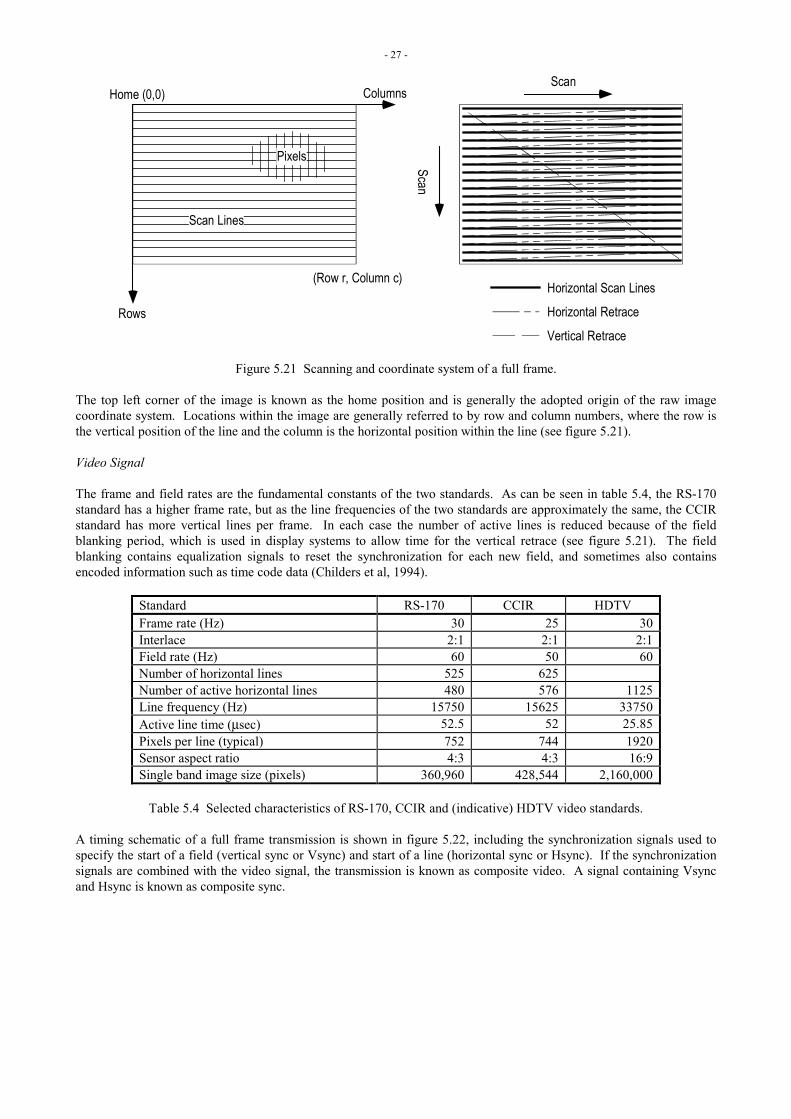
- 27 -
Figure 5.21 Scanning and coordinate system of a full frame.
The top left corner of the image is known as the home position and is generally the adopted origin of the raw image coordinate system. Locations within the image are generally referred to by row and column numbers, where the row is the vertical position of the line and the column is the horizontal position within the line (see figure 5.21). Video Signal The frame and field rates are the fundamental constants of the two standards. As can be seen in table 5.4, the RS-170 standard has a higher frame rate, but as the line frequencies of the two standards are approximately the same, the CCIR standard has more vertical lines per frame. In each case the number of active lines is reduced because of the field blanking period, which is used in display systems to allow time for the vertical retrace (see figure 5.21). The field blanking contains equalization signals to reset the synchronization for each new field, and sometimes also contains encoded information such as time code data (Childers et al, 1994).
Standard RS-170 CCIR HDTV Frame rate (Hz) 30 25 30Interlace 2:1 2:1 2:1Field rate (Hz) 60 50 60Number of horizontal lines 525 625Number of active horizontal lines 480 576 1125Line frequency (Hz) 15750 15625 33750Active line time (µsec) 52.5 52 25.85Pixels per line (typical) 752 744 1920Sensor aspect ratio 4:3 4:3 16:9Single band image size (pixels) 360,960 428,544 2,160,000
Table 5.4 Selected characteristics of RS-170, CCIR and (indicative) HDTV video standards.
A timing schematic of a full frame transmission is shown in figure 5.22, including the synchronization signals used to specify the start of a field (vertical sync or Vsync) and start of a line (horizontal sync or Hsync). If the synchronization signals are combined with the video signal, the transmission is known as composite video. A signal containing Vsync and Hsync is known as composite sync.
Rows
ColumnsHome (0,0)
Scan Lines
Pixels
Horizontal Scan Lines
Horizontal Retrace
Vertical Retrace
(Row r, Column c)
Scan
Scan

- 28 -
Figure 5.22 Timing schematic of video and synchronization signals.
A timing schematic for a single line is shown in figure 5.23, along with the horizontal sync and voltage levels. The falling edge of the synchronization pulse is the start of a new line of the field and the blanking level indicates a zero voltage level equivalent to black in the image. The peak white level is equivalent to 0.7 volts, whilst the synchronization minimum is -0.3 volts. The analogue signal is maintained within the black to white range of voltages by the clamping and clipping circuits in the camera electronics. The geometric and radiometric properties, as well as advantages and disadvantages, of such video signals are discussed in Beyer (1987, 1988) and Dähler (1987).
Figure 5.23 Timing schematic of a single line of video signal.
Neither standard specifies the frequency of sensor elements within the horizontal lines because the standards were promulgated when continuous video tube sensors were the norm. Specification of the resolution within each horizontal line was typically dependent on the quality and type video tube sensor, whereas solid state sensors have essentially discrete sensor elements. The timing of the signal output within each line can be detected by providing a pixel clock signal separately to the output video signal. Many manufacturers of CCD sensors have adopted a horizontal resolution of 752 pixels for standard RS-170 video cameras. This corresponds to a pixel clock frequency of 14.3MHz. The vertical resolution of the sensors is typically 484 lines, although only 480 lines are active. Four lines, and in most cases several or more of the columns, on the periphery of the active area are masked to give an explicit dark reference. Display and Storage
624 625 1 2 3 4 5 6 7 8 9 10 11 12 24 26 27 2825Line Count
Visible Horizontal Line574572 1 3 5
Vsync
Line Count
Visible Horizontal Line
Vsync
312 313 314 315 316 317 318 319 320 321 322 323 324311 339 340336 337
575573 0 2
338
4
Start of Odd Field
Start of Even Field
Composite Video
Composite Video
Hsync
Hsync
6
Vertical Blanking Period(Odd Field)Equalization Equalization
Serrations
Peak White Level (0.7V)
Blanking Level (0.0V)
Sync Level (-0.3V)
Analogue Signal
HsyncPulse
BackPorch
FrontPorch
HorizontalBlanking
Active Line

- 29 -
A wide variety of video monitors are available to display standard video signals in real time. The quality and features of such monitors can vary tremendously and should be appropriate to the application. CCTV systems generally use small, monochrome monitors with minimal features, whereas broadcast applications warrant large screen, colour monitors with sufficient controls to optimise the image quality. Monitors typically accept composite video and synchronization signals through a single connector for a coaxial cable. However, some monitors will accept separate synchronization signals or, for colour monitors, separate luminance and chrominance or separate red, green, blue and synchronization signals for improved colour reproduction. Storage systems for analogue video have an equally wide range of quality and features. Recording systems were initially developed to service the broadcast television industry, but over the last two decades the consumer market for video recorders has increased dramatically. Video tape cassettes dominate the industry and video cassette recorders (VCRs) are manufactured in a variety of formats, such as VHS, Video 8 and Beta. Cassette tapes, available with recording lengths from a few minutes to several hours, are a very cost-effective means of recording analogue video images. VHS, and more recently Super-VHS, recorders are most widely used in the domestic and industrial areas because this format has the highest horizontal resolution and bandwidth of the available "off the shelf" systems (Lusch, 1988). An alternative to VCRs is the 12” video disk. This type of recorder has been used widely in the broadcast industry for quick access to recorded material, but has had limited use in the domestic and industrial markets due to the greater cost of the device and the media. Recording capacities are also shorter than video tape, limited to two hours at most. However, the distinct advantage of video disk is the ability to both record and play video at frame rate, as well as randomly access individual frames. Analogue storage of video imagery requires consideration of the metric fidelity of the images during recording and subsequent playback. Aspects such as time base correctors, quality of the recording medium and the colour burst signal may significantly degrade the image geometry or radiometry. Further discussion of aspects of tape and disk recording of video images for photogrammetric applications is given in Shortis et al (1993), Höflinger and Beyer (1993), and Snow and Shortis (1995). Digital recording media for analogue images, such as broadcast quality digital video tape, have not been used to any real extent for photogrammetric applications due to the high cost of such systems. Research and development has instead concentrated on the use of computer based digital recording systems such as Photo-CD (Hanke, 1994).
5.5.2 Frame Grabbers Purpose, Principles and Functions A frame grabber is typically a printed circuit board which is designed to reside in a host computer (see figure 5.24). The purpose of a frame grabber is to instantaneously sample the output from a solid state sensor which is transmitting standard analogue video. The standard video signal is output continuously on the basis that it will be broadcast, shown on a video monitor or perhaps recorded continuously. The sample collected by the frame grabber is loaded into onboard solid state memory which is then accessible by a host computer. Stored as a contiguous array of intensity values, the fields or frame are assembled into a digital image composed of pixels structured according to the line and pixel organisation given in the previous section.
Figure 5.24 Typical frame grabber for standard analogue video input.
Depending on the application, the frame grabber may be required to intermittently sample and store individual frames, collect short sequences of frames, or perhaps continuously read the video image and carry out a real time processing task. The amount of available image memory will vary depending on the intended application of the frame grabber, as will the capability to acquire colour images from NTSC or other standard signals. Advanced capabilities include synchronous capture from a number of channels to collect multi-band or multi-camera images. Frame grabbers which are capable of real time, or near real time, processing derive this capability from onboard digital signal processors which can conduct basic image processing computations at frame rate or near frame rate. Because the frame grabber must reside in a host computer to allow access to the grabbed images, many manufacturers produce different varieties of the same basic grabber for different computer systems, such as IBM compatible PCs, Macintosh computers and Unix work stations. Even amongst these three computer types, widely adopted for support of digital imaging, there are sub-categories related to different internal communication structures. A manufacturer of frame grabbers for IBM PCs may market up to three different types of the same board.
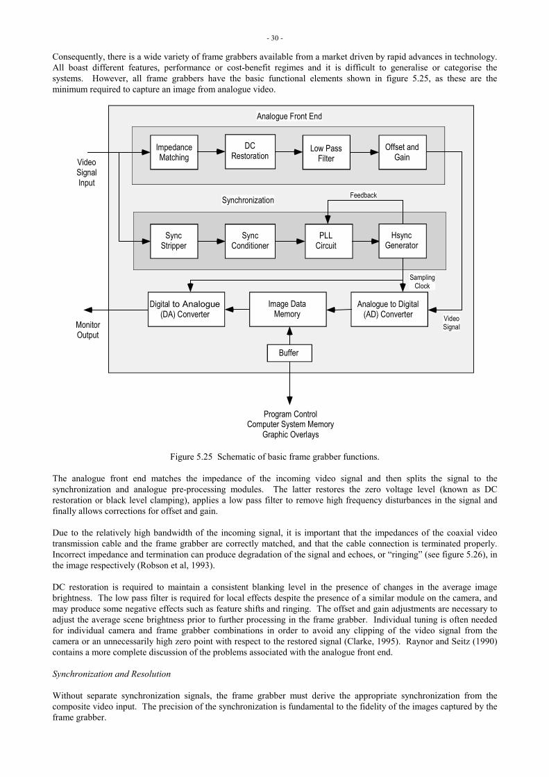
- 30 -
Consequently, there is a wide variety of frame grabbers available from a market driven by rapid advances in technology. All boast different features, performance or cost-benefit regimes and it is difficult to generalise or categorise the systems. However, all frame grabbers have the basic functional elements shown in figure 5.25, as these are the minimum required to capture an image from analogue video.
Figure 5.25 Schematic of basic frame grabber functions.
The analogue front end matches the impedance of the incoming video signal and then splits the signal to the synchronization and analogue pre-processing modules. The latter restores the zero voltage level (known as DC restoration or black level clamping), applies a low pass filter to remove high frequency disturbances in the signal and finally allows corrections for offset and gain. Due to the relatively high bandwidth of the incoming signal, it is important that the impedances of the coaxial video transmission cable and the frame grabber are correctly matched, and that the cable connection is terminated properly. Incorrect impedance and termination can produce degradation of the signal and echoes, or “ringing” (see figure 5.26), in the image respectively (Robson et al, 1993). DC restoration is required to maintain a consistent blanking level in the presence of changes in the average image brightness. The low pass filter is required for local effects despite the presence of a similar module on the camera, and may produce some negative effects such as feature shifts and ringing. The offset and gain adjustments are necessary to adjust the average scene brightness prior to further processing in the frame grabber. Individual tuning is often needed for individual camera and frame grabber combinations in order to avoid any clipping of the video signal from the camera or an unnecessarily high zero point with respect to the restored signal (Clarke, 1995). Raynor and Seitz (1990) contains a more complete discussion of the problems associated with the analogue front end. Synchronization and Resolution Without separate synchronization signals, the frame grabber must derive the appropriate synchronization from the composite video input. The precision of the synchronization is fundamental to the fidelity of the images captured by the frame grabber.
Analogue Front End
ImpedanceMatching
Low PassFilter
Offset andGainVideo
SignalInput
MonitorOutput
Synchronization
SyncConditioner
SyncStripper
Program ControlComputer System Memory
Graphic Overlays
DCRestoration
HsyncGenerator
PLLCircuit
Image DataMemory
Analogue to Digital(AD) Converter
Digital to Analogue(DA) Converter
Buffer
VideoSignal
SamplingClock
Feedback
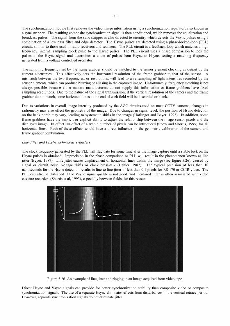
- 31 -
The synchronization module first removes the video image information using a synchronization separator, also known as a sync stripper. The resulting composite synchronization signal is then conditioned, which removes the equalization and broadcast pulses. The signal from the sync stripper is also directed to circuitry which detects the Vsync pulses using a combination of a low pass filter and edge detector. The Hsync pulses are detected using a phase-locked-loop (PLL) circuit, similar to those used in radio receivers and scanners. The PLL circuit is a feedback loop which matches a high frequency, internal sampling clock pulse to the Hsync pulses. The PLL circuit uses a phase comparison to lock the pulses to the Hsync signal and determines a count of pulses from Hsync to Hsync, setting a matching frequency generated from a voltage controlled oscillator. The sampling frequency set by the frame grabber should be matched to the sensor element clocking as output by the camera electronics. This effectively sets the horizontal resolution of the frame grabber to that of the sensor. A mismatch between the two frequencies, or resolutions, will lead to a re-sampling of light intensities recorded by the sensor elements, which can produce blurring or aliasing in the captured image. Unfortunately, frequency matching is not always possible because either camera manufacturers do not supply this information or frame grabbers have fixed sampling resolutions. Due to the nature of the signal transmission, if the vertical resolution of the camera and the frame grabber do not match, some horizontal lines at the end of each field will be discarded or blank. Due to variations in overall image intensity produced by the AGC circuits used on most CCTV cameras, changes in radiometry may also effect the geometry of the image. Due to changes in signal level, the position of Hsync detection on the back porch may vary, leading to systematic shifts in the image (Höflinger and Beyer, 1993). In addition, some frame grabbers have the implicit or explicit ability to adjust the relationship between the image sensor pixels and the displayed image. In effect, an offset of a whole number of pixels can be introduced (Snow and Shortis, 1995) for all horizontal lines. Both of these effects would have a direct influence on the geometric calibration of the camera and frame grabber combination. Line Jitter and Pixel-synchronous Transfers The clock frequency generated by the PLL will fluctuate for some time after the image capture until a stable lock on the Hsync pulses is obtained. Imprecision in the phase comparison or PLL will result in the phenomenon known as line jitter (Beyer, 1987). Line jitter causes displacement of horizontal lines within the image (see figure 5.26), caused by signal or circuit noise, voltage drifts or clock cross-talk (Dähler, 1987). The typical precision of less than 10 nanoseconds for the Hsync detection results in line to line jitter of less than 0.1 pixels for RS-170 or CCIR video. The PLL can also be disturbed if the Vsync signal quality is not good, and increased jitter is often associated with video cassette recorders (Shortis et al, 1993), especially between fields, for this reason.
Figure 5.26 An example of line jitter and ringing in an image acquired from video tape.
Direct Hsync and Vsync signals can provide for better synchronization stability than composite video or composite synchronization signals. The use of a separate Hsync eliminates effects from disturbances in the vertical retrace period. However, separate synchronization signals do not eliminate jitter.
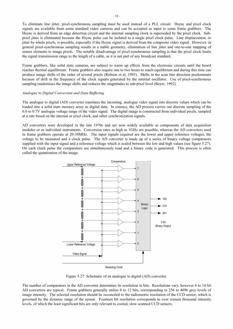
- 32 -
To eliminate line jitter, pixel-synchronous sampling must be used instead of a PLL circuit. Hsync and pixel clock signals are available from some standard video cameras and can be accepted as input to some frame grabbers. The Hsync is derived from an edge detection circuit and the internal sampling clock is superseded by the pixel clock. Sub-pixel jitter is eliminated because the Hsync pulse can be isolated to a single pixel clock pulse. Line displacement, or jitter by whole pixels, is possible, especially if the Hsync signal is derived from the composite video signal. However, in general pixel-synchronous sampling results in a stable geometry, elimination of line jitter and one-to-one mapping of sensor elements to image pixels. The notable disadvantage of pixel-synchronous sampling is that the pixel clock limits the signal transmission range to the length of a cable, as it is not part of any broadcast standard. Frame grabbers, like solid state cameras, are subject to warm up effects from the electronic circuits until the board reaches thermal equilibrium. Frame grabbers also require one to two hours to reach equilibrium and during this time can produce image shifts of the order of several pixels (Robson et al, 1993). Shifts in the scan line direction predominate because of drift in the frequency of the clock signals generated by the internal oscillator. Use of pixel-synchronous sampling randomises the image shifts and reduces the magnitudes to sub-pixel level (Beyer, 1992). Analogue to Digital Conversion and Data Buffering The analogue to digital (AD) converter translates the incoming, analogue video signal into discrete values which can be loaded into a solid state memory array as digital data. In essence, the AD process carries out discrete sampling of the 0.0 to 0.7V analogue voltage range of the video signal. The digital image is constructed from individual pixels, sampled at a rate based on the internal or pixel clock, and other synchronization signals. AD converters were developed in the late 1970s and are now widely available as components of data acquisition modules or as individual instruments. Conversion rates as high as 1GHz are possible, whereas the AD converters used in frame grabbers operate at 20-30MHz. The input signals required are the lower and upper reference voltages, the voltage to be measured and a clock pulse. The AD converter is made up of a series of binary voltage comparators supplied with the input signal and a reference voltage which is scaled between the low and high values (see figure 5.27). On each clock pulse the comparators are simultaneously read and a binary code is generated. This process is often called the quantisation of the image.
Figure 5.27 Schematic of an analogue to digital (AD) converter.
The number of comparators in the AD converter determines its resolution in bits. Resolutions vary, however 6 to 14 bit AD converters are typical. Frame grabbers generally utilise 8 to 12 bits, corresponding to 256 to 4096 grey levels of image intensity. The selected resolution should be reconciled to the radiometric resolution of the CCD sensor, which is governed by the dynamic range of the sensor. Fourteen bit resolution corresponds to over sixteen thousand intensity levels, of which the least significant bits are only relevant to cooled, slow scanned CCD sensors.
100
010
001
3 bitBinary Output
Sampling Clock
Video Signal
0
1
2
3
4
5
6
7
BinaryLogic
ComparatorsUpper Reference Voltage
Lower Reference Voltage

- 33 -
General purpose frame grabbers tend to use 8 bit converters as the association of 8 bits, or one byte of information, to one pixel is a universal standard for digital image storage. The image sizes given in table 5.4 can therefore also be read as bytes of image storage. Colour images require three bands, or three intensities per pixel, and therefore three times the storage requirement in bytes. Full colour images are commonly known as 24 bit images and have approximately 16 million possible colours. As previously noted, the storage requirement for high resolution and/or full colour images can be reduced using image compression techniques. The memory available on frame grabbers has generally increased with time due to advances in technology and the demands of higher resolution sensors. Whereas the first frame grabbers had only sufficient memory to hold a single image, the latest generation of grabbers may have up to 256Mb of onboard storage. Whilst such boards are costly, the memory is sufficient to hold approximately 740 standard RS-170 video frames, or a continuous sequence lasting almost 25 seconds. The image memory must be buffered to allow input from the AD converter with one frequency and allow read out to the host computer at a different frequency. The most recent solution to this problem is dual ported memory, which provides for simultaneous read and write access. Dual ported memory is more expensive and sophisticated than typical solid state memory, as it must arbitrate between external read access and write access by the AD converter, giving priority to the latter. The alternative is double buffering, a technique commonly used by computer graphics work stations. One part of the memory is used to write and another part is accessible for reading, leading to an effective halving of the available memory for images if simultaneous processing is required. The final function of the frame grabber is digital to analogue conversion for output of live or grabbed images to a standard video monitor. The majority of frame grabbers have additional capabilities such as graphic overlays or colourisation to identify features and a cursor to select areas of interest. Noise The electronic circuits, particularly DC restoration and the AD converter, of frame grabbers give rise to both systematic and random errors. For example, frame grabbers may exhibit non-linearity and fixed pattern noise which can be detected using averaged images grabbed from a video signal generator. These systematic errors are generally of the order of 1-2% of the peak signal (Beyer, 1992), but can be removed by image subtraction or pixel by pixel correction. Random errors are caused by quantisation noise. This is simply a noise associated with rounding error, because the continuous analogue signal is converted to one of a number of discrete levels. It can be shown that the quantisation noise is given by (Jain, 1989) :
σQ = 1
12 Q (5.6)
where Q = the quantisation step which is equivalent to approximately 0.8 mV of the analogue signal range, or 110 electrons in a full well of 105 electrons, given an 8 bit AD converter which therefore has 256 quantisation levels. The SNR attributed to quantisation noise alone is 59 dB at maximum signal level. For the combined effect from the CCD sensor and the frame grabber, quantisation noise should be added to equation 5.4 and will raise the noise floor shown in figure 5.12.
5.5.3 Slow Scan and Digital Transfers Slow scan and digital transfers have in common a closer link between the CCD sensor and the AD converter. In both cases the AD conversion process is driven by the same clock which drives the sensor output. Therefore there is no necessity for additional electronics to derive synchronization signals, which may introduce additional noise as discussed above. In effect, the quantisation function of the frame grabber is integrated into the camera (see figures 5.19 and 5.28).

- 34 -
Figure 5.28 Schematic of a digital camera.
Slow Scan Control As discussed in section 5.4.3, slow scan control is closely associated with scientific and high resolution cameras. The slow scan controller (SSC) is generally a separate module to the camera and connects directly to a specifically designed computer interface card. The SSC typically has no image memory, as this function is handled by the computer interface. The AD converter typically has a resolution of 10 to 14 bits, justified by the higher dynamic range and low noise. The intensity levels of the pixels comprising the captured image are transmitted as bits in parallel via a digital interface, which eliminates transmission noise. The disadvantages of slow scan controllers are severe limitations on cable length and slow image capture. At a 50kHz read out rate, a 1024 by 1024 pixel image requires approximately 21 seconds to be output. Still video cameras use the same principles as slow scan controllers. The essential difference being that the sensor, AD converter and image storage are all contained within a single unit. The image storage may well be a combination of a solid state frame store and disk storage. Again, image capture is slow relative to standard video systems, restricted to a few frames per second even when capturing short sequences direct to solid state memory. Both slow scan and still video systems cannot be connected to a standard video monitor because the output is incompatible. Image display for slow scan systems may be possible using the computer interface, and some still video systems, such as the original DCS100 and the recent Casio QV-10, include a small monitor screen. However, because these systems transmit digital image data, once it is stored in any computer system an image can be displayed using the computer system graphics screen, albeit at a lesser grey scale resolution than the original image acquired by SSC systems. Digital Cameras The most recent development in solid state camera technology is standard video cameras with digital output (see figure 5.17). Both analogue video and digital image data outputs are provided. A number of manufacturers have combined
Output Driver
Blanking MixAddition
Analogue Video andSynchronization
Signals
SensorClock
Generator
MasterTiming
Generator
ExternalTriggerDetect
Sensor
ControlSignals
Output Driver
Digital Data andSynchronization
Signals
Frame Store
ADconverter
Video SignalConditioning
- 35 -
digital output with progressive scanning (see section 5.4.2). Either interlaced or non-interlaced output can be selected. The analogue output is not compatible with standard video systems, such as frame grabbers and TV monitors, when non-interlaced mode is selected. In these cameras there is once more the close association between the CCD sensor and the AD converter. In addition, the cameras have sufficient onboard storage for a single frame so that an image can be grabbed and stored (see figure 5.28). This mode allows image capture to be externally triggered and read out when requested, in a similar fashion to slow scan cameras. The digital output provided on these cameras is a high speed parallel interface which requires a compatible computer interface. For example, the Pulnix TM-9700 progressive scan camera (Hori,1995) uses a differential voltage, 8 bit parallel interface operating at 14.3MHz. The data transmitted includes an equivalent to the Vsync signal which flags the start of each frame or field. As this is a digital transmission, errors will result in a missing frame, or an offset frame being loaded into the image memory, rather than an equivalent of synchronization error or line jitter. Although these cameras can output images at field and frame rates, at present there are still restrictions on the lengths of cable which can be utilised. The cameras are directly tethered to a computer system which must be within a radius of no more than approximately ten metres. In all three cases the interface or computer systems stores a digital image. The transmission of the image is virtually noise-free, but limited in range. In contrast, standard video transmission contains inherent noise, but can be transmitted at frame rate over effectively unlimited distances.
5.6 Future Developments The resolution, quality and sophistication of solid state cameras have been improving rapidly over the last two decades. The range of associated applications for digital photogrammetry and machine vision have maintained a commensurate rate of expansion. Photogrammetric and machine vision specialists have assimilated the advances in the technology of solid state sensors and have opportunistically applied new techniques to measurement tasks. There is little doubt that this trend will continue at an accelerating pace. The resolution of solid state cameras continues to increase. Sensors with a resolution of the order of 10000 by 10000 pixels are theoretically feasible (Seitz et al, 1995), but the manufacture of such large CCD arrays would have a very low yield for a sensor with few blemishes, therefore making the process very costly. However, it is likely that within a few years, cameras with a resolution of the order of 3000 by 3000 pixels will be available for very much the same price as the current generation of CCTV cameras. Cameras with linear resolutions of 9000 to 12000 pixels will probably be the upper limit for still video cameras, which will provide an image quality matching or even surpassing that of current colour slide film. The area array, still video camera will certainly become the imager of choice for photogrammetric applications which do not require a real time response, such as industrial metrology and engineering surveillance. The quality will also improve due to the widespread adoption of digital interfaces for CCTV cameras intended for standard video applications. The low noise and reliability of such cameras will improve the geometric and radiometric capabilities of real time photogrammetry and machine vision. It can also be envisioned that solid state imagers will become more sophisticated, particularly in terms of onboard intelligence (Seitz et al, 1995) to process feature recognition, extraction and correspondence. An integrated system of a solid state sensor, digital signal processors, local image memory, navigation sensors and data communications may finally realise an automated real time photogrammetric system.
5.7 References and Bibliography Amelio, G. F., Tompsett, M. F. and Smith, G. E., 1970. Experimental verification of the charge coupled device concept.
Bell System Technical Journal, 49(4) : 593-600. Beyer, H. A., 1987. Some aspects of the geometric calibration of CCD cameras. Proceedings, International Society for
Photogrammetry and Remote Sensing Intercommission Conference on the Fast Processing of Photogrammetric Data. Interlaken, Switzerland, pp. 68-81.
Beyer, H. A., 1985. Linejitter and geometric calibration of CCD-cameras. International Archives of Photogrammetry
and Remote Sensing, 27(B10): 315-324. Beyer, H. A., 1992. Geometric and radiometric analysis of a CCD-camera based photogrammetric close-range system.
Mitteilungen Nr. 51, Institute for Geodesy and Photogrammetry, ETH Zurich. 186 pages.

- 36 -
Beyer, H. A., 1993. Determination of radiometric and geometric characteristics of frame grabbers. SPIE Proceedings Volume 2067, Videometrics II, pp. 93-103.
Beyer, H. A., 1995. Digital photogrammetry in industrial applications. International Archives of Photogrammetry and
Remote Sensing, 30(5W1) : 373-375. Beynon, J. D. E. and Lamb, D. R., 1980. Charge-coupled devices and their applications. McGraw-Hill, London. 274
pages. Blouke, M. M., Heidtmann, D. L., Corrie, B., Lust, M. L. and Janesick, J. R., 1985. Large Area CCD Image Sensors for
Scientific Applications. SPIE Proceedings Volume 570, Solid State Imaging Arrays, pp. 82-85. Blouke, M. M., 1995. Charge-coupled devices meet the test as X-ray detectors. Photonics Spectra, November 1995,
pp. 118-120. Boyle, W. S. and Smith, G. E., 1970. Charge coupled semiconductor devices. Bell System Technical Journal, 49(4) :
587-593. Burner, A. W., Snow, W. L. and Goad, W. K., 1985. Close-range photogrammetry with video cameras. Proceedings,
Technical Papers, 51st American Society of Photogrammetry Annual Meeting. Washington D.C., U.S.A., pp. 62-77.
Burner, A. W., 1995. Zoom lens calibration for wind tunnel measurements. SPIE Proceedings Volume 2598,
Videometrics IV, pp. 19-33. Childers, B. A., Snow, W. L. and Shortis, M. R., 1994. Videometric system using VITC for computer-aided image
management. SPIE Proceedings Volume 2350, Videometrics III, pp. 93-95. Clarke, T. A., 1995. A frame-grabber related error in subpixel target location. Photogrammetric Record, 15(86) : 315-
322. Collet, M. G., 1985. Solid state image sensors. SPIE Proceedings Volume 591, Solid State Imagers and Their
Applications, pp. 82-93. Curry, S., Baumrind, S. and Anderson, J. M., 1986. Calibration of an array camera. Photogrammetric Engineering and
Remote Sensing, 52(5) : 627-636. Dähler, J., 1987. Problems in digital image acquisition with CCD cameras. Proceedings, International Society for
Photogrammetry and Remote Sensing Intercommission Conference on the Fast Processing of Photogrammetric Data. Interlaken, Switzerland, pp. 48-59.
Delamere, W. A., Ebben, T., Murata-Seawalt, D., Blouke, M. M., Reed, R. and Woodgate, B., 1991. The space
telescope imaging spectrograph 20482 CCD and its characteristics. SPIE Proceedings Volume 1447, Charge-Coupled Devices and Solid State Optical Sensors II, pp. 288-297.
El-Hakim, S. F. (Editor), 1993. Videometrics II. SPIE Volume 2067, Bellingham, U.S.A.. 267 pages. El-Hakim, S. F. (Editor), 1994. Videometrics III. SPIE Volume 2350, Bellingham, U.S.A.. 364 pages. El-Hakim, S. F. (Editor), 1995. Videometrics IV. SPIE Volume 2598, Bellingham, U.S.A.. 390 pages. Fraser, C. S. and Shortis M. R., 1995. Metric exploitation of still video imagery. Photogrammetric Record, 15(85):
107-122. Fraser, C. S., Shortis, M. R. and Ganci, G., 1995. Multi-sensor system self-calibration. SPIE Proceedings Volume 2598,
Videometrics IV, pp. 2-15. Fraser, C. S. and Edmundson, K. L., 1996. The metric impact of reduction optics in digital cameras. Photogrammetric
Record, 15(87) : 437-446. Fritz, L. W. and Lucas, J. R. (Editors), 1992. International Archives of Photogrammetry and Remote Sensing, Volume
29, Part B5. American Society for Photogrammetry and Remote Sensing, Bethesda, U.S.A.. 950 pages.
- 37 -
Fryer, J. G. and Shortis, M. R. (Editors), 1994. International Archives of Photogrammetry and Remote Sensing,
Volume 30, Part 5. Australian Photogrammetric and Remote Sensing Society, Melbourne, Australia. 495 pages. Furusawa, T., Mitani, N., Kitamura, Y., Kojima, K., Ikeda, T. and Ohgishi, T., 1986. A high resolution ½ inch frame
transfer CCD sensor. Journal of Imaging Technology, 12(5) : 236-240. Godding, R. and Woytowicz, D., 1995. A new digital high resolution recording system. International Archives of
Photogrammetry and Remote Sensing, 30(5W1) : 31-35. Gruen, A. and Baltsavias, E. P. (Editors), 1990. International Archives of Photogrammetry and Remote Sensing,
Volume 28, Part 5. SPIE Volume 1395, Bellingham, U.S.A.. 1245 pages. Gruen, A., Maas, H-G. and Keller, A., 1995. Kodak DCS200 - a camera for high accuracy measurements? SPIE
Proceedings Volume 2598, Videometrics IV, pp. 52-59. Gustafson, P. C. and Handley, H. B., 1992. A video-based industrial measurement system. International Archives of
Photogrammetry and Remote Sensing, 29(B5): 501-506. Hall, J. A., 1977. Can solid-state imaging devices replace television camera tubes? Optical Engineering, 16(3) : 224-
232. Hanke, K., 1994. The Photo-CD - a source and digital memory for photogrammetric images. International Archives of
Photogrammetry and Remote Sensing, 30(5) : 144-149. Hantke, D., Philipp, H., Sparrer, G. and Tschirnich, J., 1985. CCD-Zeilen sind Präzisionsmässtabe. Feingerätetächnik,
pp. 290-292. Höflinger, W. and Beyer, H. A., 1993. Evaluation of the geometric performance of a standard S-VHS camcorder. SPIE
Proceedings Volume 2067, Videometrics II, pp. 104-114. Hopkins, R., 1988. Advanced television systems. IEEE Transactions on Consumer Electronics, 34(1) : 1-15. Hopkinson, G. R., Cickshott, R. A., Purll, D. J., Skipper, M. D. and Taylor, B., 1987. Operation, performance and
reliability testing of charge-coupled devices for star trackers. Optical Engineering, 26(8) : 725-733. Hori, T., 1995. Progressive scan interline transfer CCD camera. SPIE Proceedings Volume 2416, Cameras and
Systems for Electronic Photography and Scientific Imaging, pp. 17-29. Hynecek, J., 1979. Virtual phase CCD technology. Proceedings, IEEE Electron Device Meeting (IEDM 79), pp. 611-
614. Ishihara, Y. and Tanigaki, K., 1983. A high photosensitivity IL-CCD image sensor with monolithic resin lens array.
Proceedings, IEEE Electron Device Meeting (IEDM 83), pp. 497-500. Jain, A. K., 1989. Fundamentals of Digital Image Processing. Prentice Hall, Englewood Cliffs, N.J. 592 pages. Janesick, J. R., 1989. Open pinned-phase CCD technology. SPIE Proceedings Volume 1159, EUV, X-ray and Gamma-
ray Instrumentation for Astronomy and Atomic Physics, pp. 363-371. Janesick, J. R. and Blouke, M. M., 1987. Sky on a chip : the fabulous CCD. Sky and Telescope, 74(3) : 238-242. Janesick, J. R., Hynecek, J. and Blouke, M. M., 1981. Virtual phase imager for Galileo. SPIE Proceedings Volume
290, Solid State Imagers for Astronomy, pp. 165-173. Janesick, J. R., Elliott, T., Dingizian, A., Bredthauer, R., Chandler, C., Westphal, J. and Gunn, J., 1990. New
advancements in charge-coupled device technology - sub-electron noise and 4096x4096 pixel CCDs. SPIE Proceedings Volume 1242, Charge-Coupled Devices and Solid State Optical Sensors, pp. 223-237.
Janesick, J. R. and Elliott, T., 1992. History and advancements of large area array scientific CCD imagers.
Astronomical CCD Observing and Reduction, Astronomical Society of the Pacific Conferences Series Volume 23. Bookcrafters Inc., Chelsea, Missouri, U.S.A.

- 38 -
Jurgen, R. K., 1988. High-definition television update. IEEE Spectrum, 25(4) : 56-62. Kersten, T. P. and Maas, H-G., 1994. Digital high resolution still video camera versus film-based camera in
photogrammetric industrial metrology. International Archives of Photogrammetry and Remote Sensing, 30(1): 114-121.
Klaasen, K., P., Clary, M. C. and Janesick, J. R., 1984. Charge-coupled device television camera for NASA’s Galileo
mission to Jupiter. Optical Engineering, 23(3) : 334-342. Kosonocky, W. F., Carnes, J. E., Kovac, M. G., Levine, P., Shallcross, F. V. and Rodgers, R. L., 1974. Control of
blooming in charge-coupled imagers. RCA Review, 35 : 3-24. Kristian, J. and Blouke, M. M., 1982. Charge-coupled devices in astronomy. Scientific American, 247 : 67-74. Lee, T.-H., Tredwell, T. J., Burkey, B. C., Kelly, T. M., Khosla, R. P., Losee, D. L., Neilsen. R. L. and McColgin, W.
C., 1985. A 360000-pixel charge-coupled color-image sensor for imaging photographic negative. IEEE Transactions on Electron Devices, ED32(8) : 1439-1445.
Léger, A., Omachi, T. and Wallace, G., 1991. The JPEG still video compression algorithm. Optical Engineering, 30(7)
: 947-954. Lusch, D. P., 1985. Super-VHS for improved airborne CIR videography. Proceedings, First Workshop on
Videography, ASPRS, Falls Church, U.S.A, pp. 23-29. Murphy, H. E., 1979. Performance characteristics of a producible NTSC-compatible charge-coupled device (CCD)
image sensor. SPIE Proceedings Volume 203, Recent Advances in TV Sensors and Systems, pp. 80-87. Parulski, K. A., D’Luna, L. J., Benamati, B. L. and Shelley, P. R., 1992. High-performance digital color video camera.
Journal of Electronic Imaging, 1(1) : 35-45. Peipe, J., 1995a. Photogrammetric investigation of a 3000 x 2000 pixel high resolution still video camera. International
Archives of Photogrammetry and Remote Sensing, 30(5W1): 36-39. Peipe, J., 1995b. Welche Möglichkeiten bietet High Definition Television (HDTV) für die Digitale Bildaufnahme in
der Nahbereichsphotogrammetrie? Zeitschrift für Photogrammetrie und Fernerkundung, 63(6) : 235 - 235. Peipe, J., 1995c. Photogrammetric performance evaluation of digital camera backs for in-studio and in-field use. SPIE
Proceedings Volume 2598, Videometrics IV, pp. 60-64. Pettersen, A., 1992. Metrology Norway system - an on-line industrial photogrammetry system. International Archives
Photogrammetry and Remote Sensing, 29(B5): 43-49. Pinkney, H. F. L., 1975. Theory and development of an online 30Hz video photogrammetry system for real time
dimensional control. Presented paper, International Society for Photogrammetry Commission V Symposium, Stockholm, Sweden, 38 pages.
Pol, V., Bennewitz, J. H., Jewell, T. E. and Peters, D. W., 1987. Excimer laser based lithography : a deep ultraviolet
wafer stepper for VSLI processing. Optical Engineering, 26(4) : 311-315. Purll, D. J.,1985. Solid state image sensors. Automated Visual Inspection, Edited by B. G. Batchelor, D. A. Hill and D.
C. Hodgson, IFS Publications Ltd., U.K., pp. 255-293. Raynor, J. and Seitz, P., 1990. The technology and practical problems of pixel-synchronous CCD data acquisition for
optical metrology applications. International Archives of Photogrammetry and Remote Sensing, 28(5) : 96-103. Real, R. R. and Fujimoto, Y., 1985. Stereo image transfer system with fast digital video processors and merged graphics
display. Proceedings, Technical Papers, 51st American Society of Photogrammetry Annual Meeting, Washington, U.S.A., pp. 272-283.
Robson, S., Clarke, T. A. and Chen, J., 1993. The suitability of the Pulnix TM6CN CCD camera for photogrammetric
measurement. SPIE Proceedings Volume 2067, Videometrics II, pp. 66-77.

- 39 -
Rosenberg, P., 1955. Information theory and electronic photogrammetry. Photogrammetric Engineering, 21(4) : 543-
555. Schuster, M. A. and Strull, G., 1966. A monolithic mosaic of photon sensors for solid-state imaging applications. IEEE
Transactions on Electron Devices, ED-13(12) : 907-912. Seitz, P., Vietze, O. and Spirig, T., 1995. From pixels to answers - Recent developments and trends in electronic
imaging. International Archives of Photogrammetry and Remote Sensing, 30(5W1) : 2-12. Séquin, C. H. and Tompsett, M. F., 1975. Charge transfer devices. Academic Press Inc, New York. 309 pages. Shortis, M. R., Snow, W. L., Childers, B. A. and Goad, W. K., 1993. The influence of storage media on the accuracy
and repeatability of photogrammetric measurements using CCD cameras. SPIE Proceedings Volume 2067, Videometrics II, pp. 80-92
Shortis, M. R. and Snow, W. L., 1995. Calibration of CCD cameras for field and frame capture modes. SPIE
Proceedings 2646, Conference on Digital Photogrammetry and Remote Sensing '95, pp. 2-13. Shortis, M. R., Snow, W. L. and Goad, W. K., 1995. Comparative geometric tests of industrial and scientific CCD
cameras using plumb line and test range calibrations. International Archives of Photogrammetry and Remote Sensing, 30(5W1) : 53-59.
Snow, W. L., Childers, B. A. and Shortis, M. R., 1993. The calibration of video cameras for quantitative measurements.
Proceedings, 39th International Instrumentation Symposium, Albuquerque, U.S.A., pp. 103-130. Snow, W. L. and Shortis, M. R., 1995. A rigid body motion analysis system for offline processing of time coded video
sequences. SPIE Proceedings Volume 2598, Videometrics IV, pp. 220-232. Stanton, R.H., Alexander, J.W., Dennison, E.W., Glavich, T.A. and Hovland, L.F., 1987. Optical tracking using charge-
coupled devices. Optical Engineering, 26(9) : 930-935. Stevens, E. G., Burkey, B. C., Nichols, D. N., Yee. Y., Losee, D. L., Lee, T. H. and Khosla, R. P., 1990. A 1-megapixel
IL-CCD image sensor with progressive scan, antiblooming control and lag-free operation. SPIE Proceedings Volume 1242, Charge-Coupled Devices and Solid State Optical Sensors, pp. 206-216.
Stewart, P. A. E., 1975. The application of close range X-ray photogrammetry to the study of dynamic gas turbines on
test at Rolls Royce. Presented paper, International Society for Photogrammetry Commission V Symposium, Stockholm, Sweden, 13 pages.
Streilein, A., and Gaschen, S., 1994. Comparison of a S-VHS camcorder and a high-resolution CCD-camera for use in
architectural photogrammetry. International Archives of Photogrammetry and Remote Sensing, 30(5) : 382-389. Susstrunk, S. and Holm, J., 1995. Camera data sheet for pictorial electronic still cameras. SPIE Proceedings Volume
2416, Cameras and Systems for Electronic Photography and Scientific Imaging, pp. 5-16. Tompsett, M. F., Amelio, G. F. and Smith, G. E., 1970. Charge-coupled 8-bit shift register. Applied Physics Letters,
17(3) : 111-115. Tompsett, M. F., Amelio, G. F., Bertram, W. J., Buckley, R. R., McNamara, W. J., Mikkelsen, J. C. and Sealer, D. A.,
1971. Charge-coupled imaging devices : experimental results. IEEE Transactions on Electron Devices, ED-18(11) : 992-996.
Weimer, P. K., 1975. Image sensors for solid state cameras. Advances in Electronics and Electron Physics, Volume 37,
Edited by L. Marton, Academic Press, New York, pp. 181-262. Wong, K. W., 1970. Fidelity of space TV. Photogrammetric Engineering, 36(5) : 491-497. Yang, F. H., Blouke, M. M., Heidtmann, D. L., Corrie, B., Riley, L. D. and Marsh, H. H., 1989. Trap characteristics in
large area CCD image sensors. SPIE Proceedings Volume 1071, Optical Sensors and Electronic Photography, pp. 213-228.